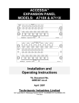
1
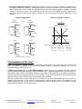
Model cPCI-75DL1 3U
SIXTEEN (16) LVDT/RVDT STIMULUS Channels
LVDT/RVDT OUTPUTS, PROGRAMMABLE
4 (3 or 4-Wire) or 8 (2-Wire)
16 BIT RESOLUTION; WRAP-AROUND SELF TEST
Optional Excitation Supply
Commercial & Military Versions Available
FEATURES:
•
•
•
•
•
•
•
•
•
•
•
•
16 Bit Resolution
Continuous background BIT testing with Reference loss detection
Power-On (POST) test
Automatically supports either 5V or 3.3V PCI bus
Transformer isolated
4 and 8 channel (2-wire) versions available or
2 and 4 channel (3 or 4 wire) versions available
Stable output with temperature
Watchdog timer and soft reset
I/O via Front Panel, P2, or both
No adjustments or trimming required
Commercial or Extended Temperature
Part number, S/N, Date code, & Rev. in nonvolatile memory
DESCRIPTION:
This card offers eight (8) two-wire, or four (4) three/four-wire transformer isolated “PROGRAMMABLE”
LVDT/RVDT outputs with wrap-around self-test and optional excitation supply. Instead of buying cards
that are set for specific outputs, the uniqueness of this design makes it possible to buy our generic card
that can be programmed and reprogrammed in the field for any excitation and signal voltage between 2.0
and 28 volts. Operating frequency between 360Hz and 10Khz can be specified (see Part Number). One
transformer isolated excitation is supplied for each A, B output pair. The output format of this card can
be configured for either two-wire or three/four-wire. The transformation ratio (TR), same for each pair of
outputs, sets the maximum output voltage with relation to the excitation voltage (TR = Max Output
Voltage / Excitation Voltage). Use of a ratio-metric design eliminates errors caused by excitation voltage
variations. The outputs are stable with temperature and switching spikes are not noticeable. A watchdog timer is
provided to monitor the processor. To simplify logistics, Part number, S/N, Date code, & Rev. are located in
nonvolatile memory locations.
Major diagnostics are incorporated to offer substantial improvements to system reliability because the user is
alerted (within 5 seconds) to channel malfunctions. This approach reduces bus traffic because the Status
registers do not require constant polling. See Programming Instructions for further details.
The (D2) test initiates automatic background BIT testing that compares the output of each channel against the
commanded input to a test accuracy of 0.2% FS and monitors each Output and Excitation. A failure triggers an
Interrupt (if enabled) and results are available in Status Registers. Testing, requires no external programming,
has no effect on the standard operation of this card and can be enabled or disabled via the bus.
The (D3) test starts a BIT test that generates and tests 20 different positions to a testing accuracy of 0.2% FS.
Results can be read from Status Registers. External reference is required. Testing requires no external
programming, and can be Initiated or terminated via the bus. CAUTION: Outputs are active during this test.
Check connected loads for possible interaction.
The POST test when enabled, will initiate a D3 test at power turn on.
Temperature Range: This board is available for "C" or "E" operating temperature ranges (See part number
designation). The "C" version operates from 0°C to +70°C and is populated with standard high quality
commercial semiconductors. The "E" version, used for severe environmental condition, operates from -40°C to
+85°C and is populated with high quality extended temperature semiconductors.
North Atlantic Industries, Inc.
110 Wilbur Place, Bohemia, NY 11716
631.567.1100/631.567.1823 (fax)
www.naii.com / e-mail:[email protected]
4/19/2005
Cage Code:OVGU1
75_DL1_A001_Rev_2.4
Page 1 of 8
SPECIFICATIONS:
Resolution:
Linearity:
Output Format:
16 bits (.001526% FS)
0.1%FS for .2 <= TR <= 2.0 (.05% FS available at a specified frequency and TR)
Configurable for either 3/4-wire or 2-wire.Transformer isolated. Output voltage will
vary directly with excitation.
Load:
With output voltages from 2.0 to 20.0Vrms: 10 kΩ min.
With output voltages from 20 to 28.0Vrms: 15 kΩ min. Short circuit protected.
Regulation:
2% max.
Excitation:
2.0 to 28 Vrms. Transformer isolated.
Frequency (excitation):
360 Hz to 10Khz, see code table
Phase Shift (input to output): 3° max
Phase shift (A/B):
0.5°.
Excitation (each) Z in:
50 KΩ min.
Interrupts:
Interface implements a single Interrupt capability. One of seven priority lines can be
selected.
Signal Logic Level:
Automatically supports either 5V or 3.3V PCI bus
Power:
+5 VDC ±5% at 0.35 A + 1A ( 3A peak ) @ 5VA Load on optional Reference
Supply
±12 VDC ±5% at 0.5 A
Temperature, operating:
"C" 0°C to +70°C, "E" -40°C to +85°C (See part number)
Temperature, storage:
-55°C to +105°C
Size:
3U (3.94" height), 4HP (0.8") width, 6.3 depth; 100mm x 20.3mm x 160mm
REFERENCE SUPPLY:
Optional. (See part number).
Voltage:
2.0-28Vrms programmable or 115Vrms fixed; resolution 0.1Vrms;
Accuracy ±2%
360 Hz to 10 kHz ±1% with 1 Hz resolution.
10% max. No load to full load.
5VA max. @ 40° min. inductive;
190mA RMS @ 2-26VAC, 45mA RMS @ 115VAC
Note: Power is reduced linearly as the Reference Voltage decreases.
Frequency:
Regulation:
Output power:
North Atlantic Industries, Inc.
110 Wilbur Place, Bohemia, NY 11716
631.567.1100/631.567.1823 (fax)
www.naii.com / e-mail:[email protected]
4/19/2005
Cage Code:OVGU1
75_DL1_A001_Rev_2.4
Page 2 of 8
Principal of Operation (LVDT): Typically the primary is excited by an ac source, causing a magnetic flux to
be generated within the transducer. Voltages are induced in the two secondaries, with the magnitude varying
with the position of the core. Usually, the secondaries are connected in series opposition, causing a net output
voltage of zero when the core is at the electrical center. When the core is displaced in either direction from
center the voltage increases linearly either in phase or out of phase with the excitation depending on the
direction.
LVDT Coil Voltage vs. Position
Output Configurations
2 WIRE
(1 CHANNEL)
2 WIRE
(2 CHANNEL)
OR
Va + Vb = K
(In-Phase)
B = Vb
A = Va-Vb
EXCITATION
EXCITATION
A = Va
Example, 10Vrms Excitation
10.0 V
Va
B = Va-Vb
5.0 V
4 WIRE
Vb
3 WIRE
B = Vb
A = Va
EXCITATION
EXCITATION
0.0 V
A = Va
0
POSITION
-FS
Va+Vb = 10V Va+Vb = 10V
Va-Vb = -10V Va-Vb = 0V
Va = 5V
Va = 0V
Vb = 5V
Vb = 10V
+FS
Va+Vb = 10V
Va-Vb = 10V
Va = 10V
Vb = 0V
B = Vb
POSITION = (Va-Vb) / (Va+Vb)
PROGRAMMING INSTRUCTIONS:
Power On Reset or System Reset: All parameters are restored to last saved setup and, if POST was
previously enabled in last setup, a D3 Test will be initiated. A power on automatic calibration test is ran and
completes in approximately 30 seconds.
Configuring Channels for 2 and 3/4-Wire Outputs: When referring to the register map make note that
there are references made to channels 1A & B through 4A & B. For channels programmed for 3/4-wire mode, the
A&B Position Data Registers are shared. Therefore, only Position Data Register A is set when configuring the
registers. The card can be programmed for use in combination, but as previously stated, the 3/4-wire channels are
paired off with the same number channel A & B and cannot be separated.
Channels programmed for 2-wire mode, the A & B outputs are set individually allowing for up to a total of 8
separate output channels. I.e., the output Ch1 A will produce a voltage equivalent to the Va-Vb voltage of a 2 wire
system representing the Position in Ch 1 A Data Register, and Ch1 B will produce the equivalent voltage
representing the Position in Ch1 B Data Register.
North Atlantic Industries, Inc.
110 Wilbur Place, Bohemia, NY 11716
631.567.1100/631.567.1823 (fax)
www.naii.com / e-mail:[email protected]
4/19/2005
Cage Code:OVGU1
75_DL1_A001_Rev_2.4
Page 3 of 8
REGISTER MEMORY MAP
000
004
008
00C
010
014
018
01C
020
024
028
02C
040
070
074
078
07C
080
084
088
08C
Position Ch.1A Data
read/write
Position Ch.1B Data (2-wire)
read/write
Position Ch.2A Data
read/write
Position Ch.2B Data (2-wire)
read/write
Position Ch.3A Data
read/write
Position Ch.3B Data (2-wire)
read/write
Position Ch.4A Data
read/write
Position Ch.4B Data (2-wire)
read/write
Transformation Ratio Ch.1
read/write
Transformation Ratio Ch.2
read/write
Transformation Ratio Ch.3
read/write
Transformation Ratio Ch.4
read/write
2-3/4 Wire Mode
read/write
Wrap-around D/L Ch.1A
read
Wrap-around D/L Ch.1B
read
Wrap-around D/L Ch.2A
read
Wrap-around D/L Ch.2B
read
Wrap-around D/L Ch.3A
read
Wrap-around D/L Ch.3B
read
Wrap-around D/L Ch.4A
read
Wrap-around D/L Ch.4B
read
090
094
098
09C
0A0
0A4
0B0
0B4
0B8
0C0
0C4
0C8
100
104
108
10C
110
114
118
11C
120
124
TABLE 1
Status, Signal
read
Status, Excitation
read
Status, Test
read
Active channels
read/write
Interrupt Status
read
Interrupt Enable
read/write
Test (D2) verify
read/write
Test Enable
read/write
Power-On (POST)
read/write
Frequency (Ref. Supply)
read/write
Voltage (Ref. Supply)
read/write
Outputs ON/OFF
read/write
Watchdog timer
read/write
Soft reset
write
Part #
read
Serial #
read
Date code
read
Rev level PCB
read
Rev level DSP
read
Rev level Interface FPGA
Rev level FPGA
read
read
Save
read/write
TABLE 1 cont.
REGISTER BIT M AP
D15
X
D14
X
D13
X
D12
X
D11
X
D10
X
D9
X
D8
X
D7
4B
D6
4A
D5
3B
D4
3A
D3
2B
D2
2A
D1
1B
D0
1A
X
X
X
X
X
X
X
X
X
X
X
X
DL4
DL3
DL2
DL1
X
X
X
X
X
X
X
X
X
X
X
X
DL4
DL3
DL2
DL1
Test Enable
X
X
X
X
X
X
X
X
X
X
X
X
D3
D2
X
X
Status, Test
X
X
X
X
X
X
X
X
4B
4A
3B
3A
2B
2A
1B
1A
Active channels
D/L outputs ON/OFF
2-3/4 W ire Mode
Status, Signal
2
3
X
X
X
X
X
X
X
X
X
4A
X
3A
X
2A
X
1A
Status, Excitation
X
X
X
X
X
X
X
X
X
4A
X
3A
X
2A
X
1A
Interrupt Enable/Status
X
X
X
X
X
X
X
X
X
X
X
X
X
TEST
REF
SIG
TABLE 2
Note 1 - Values are rounded off
Note 2 - '0' = 3 or 4 wire; '1' = 2 wire
Note 3 - Signal status is not m onitored for 2-wire m ode.
Active channels: Set the bit corresponding to each channel to be monitored during BIT testing in the Active
Channel Register (“1”=active; “0”=not used). Omitting this step will produce erroneous errors on unused
channels causing false alarms; hence unused channels will set faults, i.e. status bits, interrupts, etc.
Note: Signal status is not monitored in 2-wire mode.
Save Setup: Writing 5555h to the Save Register will save the current setup. This location will automatically clear
to 0000h when save is completed (within 5 seconds). When save is elected, all parameters are saved. However,
any parameter can be changed at any time. Saving is optional. If not saved, reenter parameters at each PowerOn. To restore factory shipped parameters, write AAAAh to the Save Register, followed by System Reset. Note:
After a SAVE or RESTORE, poll the Save Register and do not perform any operation until word is at 0000h.
To restore factory shipped parameters, write AAAAh to the Save register followed by system reset. Note:
After a Save or Restore, poll the Save register and do not perform any other operation until the Save register is
equal to "0".
Interrupt Enable Registers: Interrupts can be enabled to report specific problems/failures detected by the
card. The problem/failures that generate these interrupts are:
D/L Signal Loss, D/L Reference Loss, D/L Test Accuracy Error
North Atlantic Industries, Inc.
110 Wilbur Place, Bohemia, NY 11716
631.567.1100/631.567.1823 (fax)
www.naii.com / e-mail:[email protected]
4/19/2005
Cage Code:OVGU1
75_DL1_A001_Rev_2.4
Page 4 of 9
Each external interrupt can be enabled individually. This is accomplished by writing a “1” to the bit corresponding
interrupts to the Interrupt Enable Register and a “0” to disable those interrupts not used. Refer to Table 2.
Interrupt Status Registers: When an interrupt is initiated via a problem/failure, the Interrupt Status Register
can be interrogated by a read to identify, which interrupt occurred. Refer to Table 2. Register is latched when
interrupt is generated and unlatched when read.
Note: This register is typically read and cleared by the device driver. Subsequent readings of this register will
give clear status.
Outputs ON/OFF: Set the bit corresponding to each channel to be turned on, to “1” in the Output On/Off
Register. To turn OFF a channel, set corresponding bit to “0”. Both channels A & B are controlled
simultaneously. i.e. in 2-wire mode the A & B channel pairs are controlled concurrently. Default: Set to OFF.
2-Wire or 3/4-Wire Mode: Set the bit corresponding for each output channel pair (A & B) in the 2-3/4 Wire
Mode Register. Setting the bit to "0" => 3/4 wire mode; Setting the bit to "1" => 2 wire mode. When setting a
channel pair to 2-wire mode both channels, A & B of that number pair will be set for 2-wire. Factory default is 3/4wire mode.
Position Output: Enter the position as a 2’s complement number in the corresponding Position Ch. Data
Register within the range of -1.00 < Position < (+1.00 – lsb). In 3/4-wire mode, position is written only to the A
channel of that number pair. The B channel register is ignored. In 2-wire mode the A and B channels are set
independently. Factory default: POSITION = 0
Calculate using: register value = POSITION * 32768
Example: For a POSITION = -0.5 -> register value = -0.5 * 32768 = -16384 (0xC000)
Example: For a POSITION = 0.75 -> register value = 0.75 * 32768 = 24576 (0x6000)
The Output voltages in 3/4-wire mode are related to the position by:
Va = Excitation Voltage * TR * ( 0.5 * Position + 0.5)
Vb = Excitation Voltage * TR * ( 1 - ( 0.5 * Position + 0.5))
The Output voltage in 2-wire mode is related to the position by:
V = Excitation Input * TR * Position
Transformation Ratio (TR): Enter the transformation ratio as an integer for each channel pair (A & B) in the
Transformation Ratio Channel Register. When entering a ratio for channels that are configured for 2-wire mode,
both channels A & B of that number pair will have the same transformation ratio. Factory default TR = 1.
Set the TR using the following formula:
TR register value = TR * 1000
Example: For a TR of 0.5 -> TR register value = 0.5 * 1000 = 500 (01F4h)
The valid range of TR is: 0.00 ≤ TR ≤ 2.00.
NOTE: TR * Input Voltage must be less than 28V
Optional Excitation Output Frequency: Enter the excitation output frequency as an integer, directly in Hz in
the Frequency Register.
Example: For a Excitation Output Frequency of 1000Hz -> register value = 1000 (03E8h)
The valid range is: 360 ≤ Freq ≤ 10KHz
Factory default is: F = 400Hz
It is recommended that user program the required frequency before setting the output voltage.
Optional Excitation Output Voltage: Enter the output reference voltage as an integer in the Voltage Register.
Set the Excitation output voltage using the following formula:
Exc. Out voltage register value = V * 10
Example: For a Excitation output voltage of 7V -> register value = 7 * 10 = 70 (0046h)
The valid range is: 0.0 or 2.0 ≤ V ≤ 28.0, with 0.1 volt resolution.
Factory default is: V = 0V
Note: Units supplied with high voltage reference supply can only be set to 0.0 or 115 volts.
Power-On Self-Test (POST): The unit will initiate the D3 Test on Power-On, if POST is enabled and saved.
Enable by writing "1" or Disable by writing "0" to POST Register and then save setup.
Test Enable (D2): Writing “1” to D2 of the Test register initiates automatic background BIT testing that compares
the output of each channel with the commanded input to a testing accuracy of 0.2%FS. Results can be read from
the Test Status register. A “0” deactivates this test. This test is totally transparent to the user, requires no external
North Atlantic Industries, Inc.
110 Wilbur Place, Bohemia, NY 11716
631.567.1100/631.567.1823 (fax)
www.naii.com / e-mail:[email protected]
4/19/2005
Cage Code:OVGU1
75_DL1_A001_Rev_2.4
Page 5 of 9
programming, has no effect on the standard operation of this card and can be enabled or disabled via the bus.
Outputs must be ON and Excitation supplied for test to function. The card will (every 30 seconds) write 55h to the
Test(D2) verify register when (D2) is enabled. User can periodically clear to 00h and then after 30 seconds read
the Test (D2) verify register again to verify that background bit testing is activated.
In addition, each Excitation input and Signal output is continually monitored. Any failure triggers an Interrupt (if
enabled) and the results are available in the Signal and Excitation Status Registers. Note: Signal Monitoring is not
valid in 2 wire mode.
Test Enable (D3): Writing “1” to D3 of the Test register initiates a BIT test that generates and tests 20 different
inputs, to a testing accuracy of 0.2%FS. Test cycle takes about 45 seconds and results can be read from the Test
Status register when D3 bit changes from “1” to “0” and if enabled, an interrupt will be generated if a BIT failure is
detected (See Interrupt Register). The testing can be terminated at any time by writing "0" to D3 bit of the Test
Enable Register. Excitation is required. CAUTION: During the (D3) test, the outputs are active. Verify that
changing those outputs will not effect connected equipment.
Status, Test: Check the corresponding bit of the Test Status Register for status of BIT Testing for each active
channel. A ”1” means Accuracy OK; “0” failed. Channels that are inactive are also set to “0”. (Test cycle takes 2
seconds for accuracy error). Any Test status failure, transient or intermittent will latch the Test Status Register.
Reading will unlatch register.
Status, Excitation: Check the corresponding bit of the Excitation Status Register for status of the excitation
input for each active channel. A ”1” means Excitation ON, “0” means Excitation Loss on active channels.
Channels that are inactive are also set to “0”. (Excitation loss is detected after 2 seconds). Note: The Excitation
voltage is shared among the channel pairs, however each channel pair can have distinct external excitation
voltages. Excitation monitoring is always enabled. Any Excitation status failure, transient or intermittent will latch
the Excitation Status Register. Reading will unlatch register.
Status, Sig: Signal status is only available in 3 or 4–wire mode. Check the corresponding bit of the Signal Status
Register for status of the output signal for each active channel. A "1" means Signal is valid, “0” means Signal loss.
Channels that are inactive are also set to “0”. (Signal loss is detected after 2 seconds). Signal monitoring is always
enabled ( except in 2 wire mode ). Any Signal status failure, transient or intermittent will latch the Signal Status
Register. Reading will unlatch register.
Read Wrap-Around Position: Wrap-around positions are read from the Wrap-around D/L Ch. Registers. Each
enabled D/L channel is measured prior to the transformer output and can be read from the corresponding Wraparound D/L Register. The generated result is a 16-bit binary word (or 16-bit 2’s compliment word) that represents
position. The data is available at any time. Note: In 3/4-wire mode, only channels 1-4A need to be read.
Soft Reset: Write an integer “1” to Soft Reset Register, then clear to 0 before 50ms elapses. CAUTION:
Register is level sensitive and for proper card operation, the logic level “1”, or pulsewidth, must be <=
50ms. Considering minimum and maximum, 1 μs < pulsewidth <= 50ms. Processor reboots in about 400 ms,
after which calibration procedures begin. This function is equivalent to a power-on reset.
Watchdog timer: This feature monitors the Watchdog Timer Register. When it detects that a code has been
received, that code will be inverted within 100 µSec. The inverted code stays in the register until replaced by a new
code. The user should interrogate the Watchdog Timer Register after 100 µSec for the inverted code to confirm
that the processor is operating.
Part Number: Read as a 16 bit binary word from the Part Number Register. A unique 16 bit code is assigned
to each model number.
Serial Number: Read as a 16 bit binary word from the Serial Number Register.
Date Code: Read as decimal number from the Date Code Register.
Four digits represent YYWW (Year, Year, Week, Week)
Rev Levels: There are a total of 4 Revision Level Registers, which are listed below. Each register is defined
as 16 bits. The integer value of that particular register corresponds to the actual revision.
Rev level PCB
Rev level DSP
Rev level FPGA
Rev level Interface FPGA
Software - PCI Programming
North Atlantic Industries, Inc.
110 Wilbur Place, Bohemia, NY 11716
631.567.1100/631.567.1823 (fax)
www.naii.com / e-mail:[email protected]
4/19/2005
Cage Code:OVGU1
75_DL1_A001_Rev_2.4
Page 6 of 9
This section provides programmers the information needed for developing drivers other than those supplied.
The following information resides in the PCI configuration registers:
Device ID
Vendor ID
Rev
Subsystem ID
= 7541
= 15AC
= 01
= 000115AC
(hex)
(hex)
(hex)
(hex)
Base Address
= Assigned by the PCI BIOS. Interrogate the PCI BIOS for this information.
Required Address space = 1K for each card.
CONNECTOR J2
J2D-20
Exc. Out Lo
J2E-18
CH4 B Lo
J2F-22
GND
J2D-21
Exc. Out Hi
J2E-21
CH4 B Hi
J2F-21
GND
J2D-20
N/C
J2E-20
CH4 A Hi
J2F-20
GND
J2D-19
N/C
J2E-19
CH4 A Lo
J2F-19
GND
J2D-18
Exc. 4 A-B Lo
J2E-18
N/C
J2F-18
GND
J2D-17
Exc. 4 A-B Hi
J2E-17
N/C
J2F-17
GND
J2D-16
N/C
J2E-16
CH3 B Lo
J2F-16
GND
J2D-15
N/C
J2E-15
CH3 B Hi
J2F-15
GND
J2D-14
N/C
J2E-14
CH3 A Hi
J2F-14
GND
J2D-13
N/C
J2E-13
CH3 A Lo
J2F-13
GND
J2D-12
Exc. 3 A-B Lo
J2E-12
N/C
J2F-12
GND
J2D-11
Exc. 3 A-B Hi
J2E-11
N/C
J2F-11
GND
J2D-10
N/C
J2E-10
CH2 B Lo
J2F-10
GND
J2D-9
N/C
J2E-9
CH2 B Hi
J2F-9
GND
J2D-8
N/C
J2E-8
CH2 A Hi
J2F-8
GND
J2D-7
N/C
J2E-7
CH2 A Lo
J2F-7
GND
J2D-6
Exc. 2 A-B Lo
J2E-6
N/C
J2F-6
GND
J2D-5
Exc. 2 A-B Hi
J2E-5
N/C
J2F-5
GND
J2D-4
N/C
J2E-4
CH1 B Lo
J2F-4
GND
J2D-3
N/C
J2E-3
CH1 B Hi
J2F-3
GND
J2D-2
Exc. 1 A-B Lo
J2E-2
CH1 A Hi
J2F-2
GND
J2D-1
Exc. 1 A-B Hi
J2E-1
CH1 A Lo
J2F-1
GND
TABLE 3
As of June 1, 2004 S4-CH4 and RLO-OUT has been moved from E22 and D22 to E18 and D20 respectively to support cPCI
Geographical Addressing.
P1 - Front Connector DC37P; Mate: DC37S
Pin
Designation
Pin
Designation
Pin
35
CH1 A Lo
10
Exc. 2 A-B Lo
1
Designation
CH4 A Hi
16
CH1 B Hi
29
Exc. 2 A-B Hi
2
CH4 B Lo
17
CH1 A Hi
25
CH3 A Lo
3
Exc. 4 A-B Lo
34
CH1 B Lo
8
CH3 B Hi
22
Exc. 4 A-B Hi
15
Exc. 1 A-B Lo
7
CH3 A Hi
19
Exc. Out Lo
33
Exc. 1 A-B Hi
26
CH3 B Lo
37
Exc. Out Hi
12
CH2 A Lo
6
Exc. 3 A-B Lo
30
CH2 B Hi
24
Exc. 3 A-B Hi
31
CH2 A Hi
20
CH4 A Lo
11
TABLE 4
CH2 B Lo
21
CH4 B Hi
North Atlantic Industries, Inc.
110 Wilbur Place, Bohemia, NY 11716
631.567.1100/631.567.1823 (fax)
www.naii.com / e-mail:[email protected]
4/19/2005
Cage Code:OVGU1
75_DL1_A001_Rev_2.4
Page 7 of 9
CODE TABLE
Code
Frequency (Hz) Notes
01
400
02
2.8k - 3.2K
03
2K
04
2.69K
05
3K
See code list addendum for descriptions of code 50 and above.
TABLE 5
PART NUMBER DESIGNATION
75DL1 - X X L X X X - XX
TOTAL NUMBER OF CHANNELS
CODE (See Code Table)
2 = 2 Channels of 3 or 4 wire
OR 4 channels of 2 wire
4 = 4 Channels of 3 or 4 wire
OR 8 channels of 2 wire
OPTIONS
0 = NONE
ENVIRONMENTAL
C = 0°C to +70°C
E = -40°C to +85°C
H = E With Removable Conformal Coating
K = C With Removable Conformal Coating
OPTIONAL REFERENCE SELECTION
0 = No “On Board Reference”
A = 2-28 VRMS output
C = 115 VRMS fixed output
contact factory for other temperature requirements
MECHANICAL
F = Front Panel I/O
P = Rear I/O only
B = Front Panel I/O and Rear I/O
Note: J2 connections can not be used for
Analog signals in a PXI chassis. Analog
Outputs must be via the front panel I/O only (F).
North Atlantic Industries, Inc.
110 Wilbur Place, Bohemia, NY 11716
631.567.1100/631.567.1823 (fax)
www.naii.com / e-mail:[email protected]
4/19/2005
Cage Code:OVGU1
75_DL1_A001_Rev_2.4
Page 8 of 9
Revision Page
Revision
1
Description of Change
Original
Engineer
Date
FH
07/262001
1.4
Added memory map, register map and connector information; Added descriptions and
explanation for configuring 2 & 4 wire. Added code 05 - 3Khz to code table. Modified title, part
number(X->L); Revised reference: added 115V
FH/BC
11/09/01
1.5
Removed reference made to VME in specifcations; Changed "M" to "E" in spec. & PN. Added
note in PN for J2 connections in PXI Chassis.
FH/BC
11/27/01
1.6
See code list addendum for descriptions of code 50 and above.
Part Number: contact factory for other temperature requirements.
Updated PN, Mech. Formatting. Automatically supports either 5V or 3.3V logic levels.
GS
02/06/02
1.7
For proper Soft Reset operation, 1μ < pulsewidth <=50ms.
GS
6/27/02
1.8
Update LARGE DL Graphic
GS
6/27/02
1.9
Removed 2-13.5 volt reference option (from spec, and PN)
GS
6/28/02
2.1
PN Total number of A & B channels -> Total number of channels (A& B deleted)
GS
1/28/4
2.2
GS
7/7/4
2.3
Conducted cooled versions available. As of June 1, 2004 S4-CH4 and RLO-OUT has been
moved from E22 and D22 to E18 and D20 respectively to support cPCI Geographical
Addressing
Removes Wedgelock option from PN. Conduction cooled version is NOT available
GS
4/19/5
2.4
Changed Address
DD
05/07/07
North Atlantic Industries, Inc.
110 Wilbur Place, Bohemia, NY 11716
631.567.1100/631.567.1823 (fax)
www.naii.com / e-mail:[email protected]
4/19/2005
Cage Code:OVGU1
75_DL1_A001_Rev_2.4
Page 9 of 9