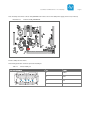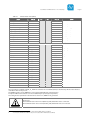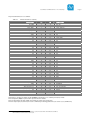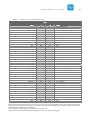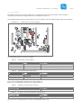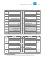
1
STKP2020
User's Manual
STKP2020 UM 100
17.10.2011
User's Manual l STKP2020 UM 100 l © 2011 TQ-Group
Page i
TABLE OF CONTENTS
1.
1.1
1.2
1.3
1.4
1.5
1.6
1.7
1.8
1.9
1.10
2.
3.
3.1
3.2
3.2.1
3.2.2
3.2.3
3.3
3.3.1
3.3.1.1
3.3.1.2
3.3.1.3
3.3.1.4
3.3.1.5
3.3.1.6
3.3.1.7
3.3.1.8
3.3.1.9
3.3.1.10
3.3.1.11
3.3.1.12
3.3.1.13
3.3.2
3.3.2.1
3.3.2.2
3.3.2.3
3.3.2.4
3.3.2.5
3.3.3
3.3.3.1
3.3.3.2
3.3.3.3
3.3.3.4
3.3.3.5
3.3.3.6
3.3.3.7
3.3.3.8
3.3.3.9
3.3.3.9.1
3.3.3.9.2
3.3.3.9.3
3.3.3.9.4
3.3.3.9.5
3.3.3.9.6
3.3.3.9.7
3.3.3.9.8
3.3.3.9.9
3.3.3.10
ABOUT THIS MANUAL......................................................................................................................................................................................1
Copyright and licence expenses ..................................................................................................................................................................1
Registered trademarks ....................................................................................................................................................................................1
Disclaimer............................................................................................................................................................................................................1
Imprint..................................................................................................................................................................................................................1
Tips on safety......................................................................................................................................................................................................2
Symbols and typographic conventions .....................................................................................................................................................2
Handling and ESD tips.....................................................................................................................................................................................2
Naming of signals .............................................................................................................................................................................................3
Further applicable documents / presumed knowledge .......................................................................................................................3
Acronyms and definitions ..............................................................................................................................................................................4
BRIEF DESCRIPTION ..........................................................................................................................................................................................5
TECHNICAL DATA..............................................................................................................................................................................................6
Functionality and system architecture overview ....................................................................................................................................6
Technical data overview .................................................................................................................................................................................7
Technical data electronics..............................................................................................................................................................................7
Technical data mechanics ..............................................................................................................................................................................8
Component placement...................................................................................................................................................................................8
Electronics specification .................................................................................................................................................................................9
External interfaces ............................................................................................................................................................................................9
Power supply......................................................................................................................................................................................................9
COM1 (RS232).................................................................................................................................................................................................. 11
COM2 (RS232).................................................................................................................................................................................................. 12
On-board gigabit Ethernet.......................................................................................................................................................................... 13
USB ..................................................................................................................................................................................................................... 15
SD card slot ...................................................................................................................................................................................................... 17
COP/JTAG P2020 ............................................................................................................................................................................................ 19
JTAG chain........................................................................................................................................................................................................ 20
UART................................................................................................................................................................................................................... 21
SPI ....................................................................................................................................................................................................................... 23
GPIO ................................................................................................................................................................................................................... 24
IEEE® 1588......................................................................................................................................................................................................... 25
I2C ........................................................................................................................................................................................................................ 26
Internal interfaces .......................................................................................................................................................................................... 27
PCIe slots........................................................................................................................................................................................................... 27
FlexiFace® 1 (2 × gigabit Ethernet) ........................................................................................................................................................... 30
FlexiFace® 2 (1 × gigabit Ethernet) ........................................................................................................................................................... 32
Local bus slot................................................................................................................................................................................................... 34
Fan connector ................................................................................................................................................................................................. 37
System components ..................................................................................................................................................................................... 38
Processor board TQMP2020 ....................................................................................................................................................................... 38
SERDES clock generation............................................................................................................................................................................. 43
Ethernet clock generation........................................................................................................................................................................... 45
I2C-bus................................................................................................................................................................................................................ 46
I2C I/O expander 1 (DIP switches, push-buttons) ................................................................................................................................. 47
I2C I/O expander 2 (LEDs)............................................................................................................................................................................. 48
JTAG chain........................................................................................................................................................................................................ 51
Battery socket.................................................................................................................................................................................................. 53
Power supply................................................................................................................................................................................................... 54
Power supply block diagram...................................................................................................................................................................... 54
Input power supply ....................................................................................................................................................................................... 54
Voltage generation 5 V................................................................................................................................................................................. 54
Voltage generation 3.3 V and 3.3 V PCIe................................................................................................................................................. 54
Voltage generation 2.5 V ............................................................................................................................................................................. 56
Voltage generation 12 V PCIe..................................................................................................................................................................... 56
LED V810: 12 V PCIE ERR............................................................................................................................................................................... 57
Current measurement .................................................................................................................................................................................. 57
Power consumption...................................................................................................................................................................................... 58
Voltage supervision and reset generation ............................................................................................................................................. 59
User's Manual l STKP2020 UM 100 l © 2011 TQ-Group
Page ii
TABLE OF CONTENTS (continued)
3.3.4
3.3.4.1
3.3.4.2
3.3.4.3
3.3.4.4
3.3.4.5
3.3.4.6
3.3.4.7
3.3.4.8
4.
5.
5.1
5.2
6.
6.1
6.2
6.2.1
6.2.2
User's interfaces.............................................................................................................................................................................................. 59
On-off switch ................................................................................................................................................................................................... 59
Reset push-button......................................................................................................................................................................................... 59
User DIP switches........................................................................................................................................................................................... 60
User push-buttons......................................................................................................................................................................................... 60
User LEDs .......................................................................................................................................................................................................... 60
Status / Error LEDs.......................................................................................................................................................................................... 60
Ethernet LEDs.................................................................................................................................................................................................. 60
SERDES clock DIP switch.............................................................................................................................................................................. 60
SOFTWARE SPECIFICATION......................................................................................................................................................................... 61
SAFETY REQUIREMENTS AND PROTECTIVE REGULATIONS............................................................................................................... 61
EMC characteristics........................................................................................................................................................................................ 61
Operational safety and personal security............................................................................................................................................... 61
CLIMATIC AND OPERATIONAL CONDITIONS......................................................................................................................................... 61
Reliability and product life .......................................................................................................................................................................... 61
Environment protection .............................................................................................................................................................................. 61
RoHS compliance ........................................................................................................................................................................................... 61
Other entries.................................................................................................................................................................................................... 61
User's Manual l STKP2020 UM 100 l © 2011 TQ-Group
Page iii
TABLE DIRECTORY
Table 1:
Table 2:
Table 3:
Table 4:
Table 5:
Table 6:
Table 7:
Table 8:
Table 9:
Table 10:
Table 11:
Table 12:
Table 13:
Table 14:
Table 15:
Table 16:
Table 17:
Table 18:
Table 19:
Table 20:
Table 21:
Table 22:
Table 23:
Table 24:
Table 25:
Table 26:
Table 27:
Table 28:
Table 29:
Table 30:
Table 31:
Table 32:
Table 33:
Table 34:
Table 35:
Table 36:
Table 37:
Table 38:
Table 39:
Table 40:
Table 41:
Table 42:
Table 43:
Table 44:
Table 45:
Table 46:
Table 47:
Table 48:
Table 49:
Table 50:
Table 51:
Table 52:
Table 53:
Table 54:
Table 55:
Table 56:
Table 57:
Table 58:
Terms and Conventions ............................................................................................................................................................................2
Acronyms.......................................................................................................................................................................................................4
Pinout of power supply connector (X601) ..........................................................................................................................................9
Suitable mating plug (power supply connector) for X601.............................................................................................................9
Pinout of power supply terminal (X600)..............................................................................................................................................9
Pinout of header for external power-on (X630).............................................................................................................................. 10
Used type of connector (header for external power-on)............................................................................................................. 10
Pinout of COM1 (X210, D-sub connector) ........................................................................................................................................ 11
Pinout of COM2 (X210, D-sub connector) ........................................................................................................................................ 12
Pinout of Ethernet jack (X380) ............................................................................................................................................................. 14
Pinout of USB jack.................................................................................................................................................................................... 16
Pinout of SD card slot (X200)................................................................................................................................................................ 17
Pinout of COP/JTAG (X230) ................................................................................................................................................................... 19
Used type of connector (COP/JTAG) .................................................................................................................................................. 19
Pinout of JTAG chain header (X240)................................................................................................................................................... 20
Used type of connector (JTAG chain header).................................................................................................................................. 20
Pinout of UART header (X130) ............................................................................................................................................................. 22
Used type of connector (UART header)............................................................................................................................................. 22
Pinout of SPI header (X140) .................................................................................................................................................................. 23
Used type of connector (SPI header) ................................................................................................................................................. 23
Pinout of GPIO header (X150) .............................................................................................................................................................. 24
Used type of connector (GPIO header).............................................................................................................................................. 24
Pinout of IEEE® 1588 header (X410).................................................................................................................................................... 25
Used type of connector (IEEE® 1588 header)................................................................................................................................... 25
Pinout of I2C 1 header (X160)................................................................................................................................................................ 26
Pinout of I2C 2 header (X170)................................................................................................................................................................ 26
Used type of connector (I2C 1 header)............................................................................................................................................... 26
Used type of connector (I2C 2 header)............................................................................................................................................... 26
Pinout of PCIe-slot 1 (X450) .................................................................................................................................................................. 28
Pinout of PCIe-Slot 2 (X470).................................................................................................................................................................. 29
Pinout of FlexiFace® 1 (X400)................................................................................................................................................................ 31
Pinout of FlexiFace® 2 (X900)................................................................................................................................................................ 33
Pinout of local bus slot (X550).............................................................................................................................................................. 35
Pinout of fan connector (X621)............................................................................................................................................................ 37
Pinout of jumper fan voltage (X620).................................................................................................................................................. 37
Used type of connector (fan connector)........................................................................................................................................... 37
Used type of connector (Jumper fan voltage header).................................................................................................................. 37
Pinout of TQMP2020 module connector (X100) ............................................................................................................................ 39
Pinout of TQMP2020 module connector (X120) ............................................................................................................................ 40
Pinout of TQMP2020 module connector (X110) ............................................................................................................................ 42
Used parts (connectors to the processor board)............................................................................................................................ 42
SERDES reference frequency per protocol....................................................................................................................................... 43
Configuration of SERDES clock frequency........................................................................................................................................ 44
Configuration of SERDES clock spread spectrum .......................................................................................................................... 44
Assignment of I2C I/O expander 1 to DIP switches and push-buttons .................................................................................... 47
Assignment of I2C I/O expander 2 to LEDs ....................................................................................................................................... 48
Pinout of LED jumper header (X260) ................................................................................................................................................. 50
Pinout of additional header for extension board (X261) ............................................................................................................. 50
Used type of connector (LED jumper header)................................................................................................................................. 50
Used type of connector (additional header for extension board) ............................................................................................ 50
Pinout of JTAG test connector (X240)................................................................................................................................................ 52
Used type of connector (JTAG test connector)............................................................................................................................... 52
Pinout of RTC battery external supply / measurement (X610, X611)....................................................................................... 53
Current measurement on the STKP2020 .......................................................................................................................................... 57
Current consumption STKP2020 in different load scenarios...................................................................................................... 58
Voltages and currents on the STKP2020........................................................................................................................................... 58
Pinout of HRESET_REQ# jumper (X871) ............................................................................................................................................ 59
Used type of connector (HRESET_REQ# jumper) ........................................................................................................................... 59
User's Manual l STKP2020 UM 100 l © 2011 TQ-Group
Page iv
ILLUSTRATION DIRECTORY
Illustration 1:
Illustration 2:
Illustration 3:
Illustration 4:
Illustration 5:
Illustration 6:
Illustration 7:
Illustration 8:
Illustration 9:
Illustration 10:
Illustration 11:
Illustration 12:
Illustration 13:
Illustration 14:
Illustration 15:
Illustration 16:
Illustration 17:
Illustration 18:
Illustration 19:
Illustration 20:
Illustration 21:
Illustration 22:
Illustration 23:
Illustration 24:
Illustration 25:
Illustration 26:
Illustration 27:
Illustration 28:
Illustration 29:
Illustration 30:
Illustration 31:
Illustration 32:
Illustration 33:
Illustration 34:
Illustration 35:
Illustration 36:
Illustration 37:
Illustration 38:
Illustration 39:
Illustration 40:
Illustration 41:
Illustration 42:
Illustration 43:
Illustration 44:
Illustration 45:
STKP2020 image ..................................................................................................................................................................................5
STKP2020 block diagram...................................................................................................................................................................6
Top view STKP2020.............................................................................................................................................................................8
Position of power supply connectors............................................................................................................................................9
Position of on-off switch and header for external power-on.............................................................................................. 10
Position of COM1 interface............................................................................................................................................................ 11
Position of COM2 interface............................................................................................................................................................ 12
On-board gigabit Ethernet interface, schematic illustration .............................................................................................. 13
Position of on-board gigabit Ethernet interface..................................................................................................................... 13
Position of SGMII configuration-EEPROM and header.......................................................................................................... 14
Position of USB jack.......................................................................................................................................................................... 15
Position of USB_PWR_OK LED ...................................................................................................................................................... 15
Position of USB_PWR ERR LED...................................................................................................................................................... 16
Position of SD card slot ................................................................................................................................................................... 17
Position of COP/JTAG connector ................................................................................................................................................. 19
Position of JTAG chain header...................................................................................................................................................... 20
UART interfaces, schematic illustration ..................................................................................................................................... 21
Position of UART header................................................................................................................................................................. 21
Position of SPI header ..................................................................................................................................................................... 23
Position of GPIO header.................................................................................................................................................................. 24
Position of IEEE® 1588 header....................................................................................................................................................... 25
Position of I2C headers .................................................................................................................................................................... 26
Position of PCIe slots........................................................................................................................................................................ 27
FlexiFace® 1, schematic illustration............................................................................................................................................. 30
Position of FlexiFace® 1 - slot ........................................................................................................................................................ 30
FlexiFace® 2, schematic illustration............................................................................................................................................. 32
Position of FlexiFace® 2 slot........................................................................................................................................................... 32
Position of local bus slot................................................................................................................................................................. 34
Position of fan connector and jumper ....................................................................................................................................... 37
Position of plug connectors for TQMP2020 ............................................................................................................................. 38
Position of DIP switch for SERDES clock parametrisation .................................................................................................... 43
Position of jumper for Ethernet clock selection...................................................................................................................... 45
Wiring of I2C buses ........................................................................................................................................................................... 46
Position of DIP switches and push-buttons.............................................................................................................................. 47
Position of user LEDs and jumpers.............................................................................................................................................. 48
Position of X621 for extension board GPIO .............................................................................................................................. 49
Architecture of JTAG chain ............................................................................................................................................................ 51
Position of JTAG test connector................................................................................................................................................... 52
Position of battery socket .............................................................................................................................................................. 53
Power supply block diagram ........................................................................................................................................................ 54
Position of headers “3.3 V measuring resistors”...................................................................................................................... 55
Position of Error-LEDs VCC3V3, VCC3V3_PCIE......................................................................................................................... 55
Position of header “12 V PCIe measuring resistor”................................................................................................................. 56
Position of Error-LED VCC12V_PCIE ............................................................................................................................................ 57
Position of HRESET_REQ# jumper ............................................................................................................................................... 59
User's Manual l STKP2020 UM 100 l © 2011 TQ-Group
REVISION HISTORY
Rev.
Date
Name
100
17.10.2011
Petz
Pos.
Modification
Document created
Page v
User's Manual l STKP2020 UM 100 l © 2011 TQ-Group
Page 1
1. ABOUT THIS MANUAL
1.1 Copyright and licence expenses
Copyright protected © 2011 by TQ-Systems GmbH.
This User’s Manual may not be copied, reproduced, translated, changed or distributed, completely or partially in electronic,
machine readable, or in any other form without the written consent of TQ-Systems GmbH.
The drivers and utilities for the used components as well as the BIOS are subject to the copyrights of the respective
manufacturers. The licence conditions of the respective manufacturer are to be adhered to.
Bootloader-licence expenses are paid by TQ-Systems and are included in the price.
Licence expenses for the operating system and applications are not taken into consideration and must be separately calculated /
declared.
1.2 Registered trademarks
TQ-Systems GmbH aims to adhere to the copyrights of all the graphics and texts used in all publications, and strives to use
original or license-free graphics and texts.
All the brand names and trademarks mentioned in the publication, including those protected by a third party, unless specified
otherwise in writing, are subjected to the specifications of the current copyright laws and the proprietary laws of the present
registered proprietor without any limitation. One should conclude that brand and trademarks are rightly protected by of a third
party.
1.3 Disclaimer
TQ-Systems GmbH does not guarantee that the information in this manual is up-to-date, correct, complete or of good quality.
Nor does TQ-Systems assume guarantee for further usage of the information. Liability claims against TQ-Systems GmbH,
referring to material or non-material related damages caused, due to usage or non-usage of the information given in the manual,
or due to usage of erroneous or incomplete information, are exempted, as long as there is no proven intentional or negligent
fault of TQ-Systems GmbH.
TQ-Systems GmbH explicitly reserves the rights to change or add to the contents of this manual or parts of it without special
notification.
1.4 Imprint
TQ-Systems GmbH
Gut Delling, Mühlstraße 2
82229 Seefeld
Tel:
+49 (0) 8153 9308–0
Fax:
+49 (0) 8153 9308–134
Email: [email protected]
Web:
http://www.tq-group.com/
User's Manual l STKP2020 UM 100 l © 2011 TQ-Group
Page 2
1.5 Tips on safety
Improper or incorrect handling of the product can substantially reduce its life span.
1.6 Symbols and typographic conventions
Table 1:
Symbol
Terms and Conventions
Meaning
This symbol represents the handling of electrostatic-sensitive modules and / or components. These
components are often damaged / destroyed by the transmission of a voltage higher than about 50 V.
A human body usually only experiences electrostatic discharges above approximately 3,000 V.
This symbol indicates the possible use of voltages higher than 24 V.
Please note the relevant statutory regulations in this regard.
Non-compliance with these regulations can lead to serious damage to your health and also cause
damage / destruction of the component.
This symbol indicates a possible source of danger. Acting against the procedure described can lead to
possible damage to your health and / or cause damage / destruction of the material used.
This symbol represents important details or aspects for working with TQ-products.
Command
A font with fixed-width is used to denote commands, file names, or menu items.
1.7 Handling and ESD tips
General handling of your TQ-products
The TQ-product may only be used and serviced by certified personnel who have taken note of the
information, the safety regulations in this document and all related rules and regulations.
A general rule is: do not touch the TQ-product during operation. This is especially important when
switching on, changing jumper settings or connecting other devices without ensuring beforehand
that the power supply of the system has been switched off.
Violation of this guideline may result in damage / destruction of the module and be dangerous to your
health.
Improper handling of your TQ-product would render the guarantee invalid.
Proper ESD handling
The electronic components of your TQ-product are sensitive to electrostatic discharge (ESD).
Always wear antistatic clothing, use ESD-safe tools, packing materials etc., and operate your TQproduct in an ESD-safe environment. Especially when you switch modules on, change jumper settings,
or connect other devices.
User's Manual l STKP2020 UM 100 l © 2011 TQ-Group
Page 3
1.8 Naming of signals
A hash mark (#) at the end of the signal name indicates a low-active signal.
Example: RESET#
If a signal can switch between two functions and if this is noted in the name of the signal, the low-active function is marked with
a hash mark and shown at the end.
Example: C / D#
If a signal has multiple functions, the individual functions are separated by slashes when they are important for the wiring.
The identification of the individual functions follows the above conventions.
Example: WE2# / OE#
1.9 Further applicable documents / presumed knowledge
•
Specifications and manual of the used modules:
These documents describe the service, functionality and special characteristics of the used module (incl. BIOS).
•
Specifications of the used components:
The manufacturer's specifications of the used components, for example CompactFlash cards, are to be taken note of.
They contain, if applicable, additional information that must be taken note of for safe and reliable operation.
These documents are stored at TQ-Systems.
•
Chip errata:
It is the user's responsibility to make sure all errata published by the manufacturer of each component are taken note of.
The manufacturer’s advice should be followed.
•
Software behaviour:
No warranty can be given, nor responsibility taken for any unexpected software behaviour due to deficient
components.
•
General expertise:
Expertise in electrical engineering / computer engineering is required for the installation and the use of the device.
The following documents are required to fully comprehend the following contents:
•
•
•
•
•
Circuit diagram STKP2020.SP.0100.pdf
CPU Manual P2020: P2020RM.pdf, P2020EEC_RevF.pdf
User’s Manual TQMP2020.UM.100
Documentation of boot loader U-Boot (http://www.denx.de/wiki/U-Boot/Documentation)
Documentation of ELDK (http://www.denx.de/wiki/DULG/ELDK)
User's Manual l STKP2020 UM 100 l © 2011 TQ-Group
1.10 Acronyms and definitions
The following acronyms and abbreviations are used in this document:
Table 2:
Acronyms
Acronym
Meaning
CPU
Central Processing Unit
COP
Common On-chip Processor
DIN
Deutsche Industrie Norm
DC
Direct Current
DC/DC
Direct Current/Direct Current
DIP
Dual In-line Package
EEPROM
Electrically Erasable Programmable Read-only Memory
EMC
Electro-Magnetic Compatibility
ESD
Electro-Static Discharge
eSDHC
Enhanced Secure Digital High Capacity
eTSEC
Enhanced Three-Speed Ethernet Controller
GPIO
General Purpose Input/Output
Gbps
Gigabit per second
IP
Ingress Protection
I/O
Input/Output
IEEE®
Institute of Electrical and Electronics Engineers
I2C
Inter-Integrated Circuit
JTAG
Joint Test Action Group
LED
Light Emitting Diode
LDO
Low Drop-Out
PCI
Peripheral Component Interconnect
PCIe
Peripheral Component Interconnect express
Phy
Physical (interface)
PCB
Printed Circuit Board
PLD
Programmable Logic Device
PD
Pull-Down (resistor)
PQ
Product Qualification
PU
Pull-Up (resistor)
RTC
Real-Time Clock
RS232
Recommended Standard (serial interface)
RGMII
Reduced Gigabit Media Independent Interface
RJ45
Registered Jack 45
RoHS
Restriction of (the use of certain) Hazardous Substances
SD-Card
Secure Digital Card
SDHC
Secure Digital High Capacity
SD/MMC
Secure Digital Multimedia Card
SGMII
Serial Gigabit Media Independent Interface
SPI
Serial Peripheral Interface
SERDES
Serializer/Deserializer
UART
Universal Asynchronous Receiver/Transmitter
USB
Universal Serial Bus
WEEE
Waste Electrical and Electronic Equipment
Page 4
User's Manual l STKP2020 UM 100 l © 2011 TQ-Group
Page 5
2. BRIEF DESCRIPTION
Illustration 1:
STKP2020 image
The Starterkit STKP2020 serves as a baseboard for the module TQMP2020.
It is a reference platform with which the functions of the TQMP2020 can be shown and evaluated.
The module TQMP2020 is based on the Freescale QorIQ-CPU P2020.
Models with pin-compatible processors (P2010, P1020, P1011, P1021, and P1012) are also possible.
The Starterkit STKP2020 also serves as a baseboard for these models.
The following features mark the advantage of the Starterkit:
•
Saving in time by early adaptation of software components on the target system.
•
Users who design their own mainboard receive the circuit diagrams of the starter kit from TQ-Systems.
The user saves time, because frequently required parts of the circuit can be taken over from the schematic.
•
Risk minimisation by being able to evaluate single system requirements before completion of the whole system, e.g.,
test of response times, transfer speeds, CPU performance, thermal behaviour etc.
•
Minimisation of risk and time saving by being able to test customised functions, e.g., for PCI or PCIe or similar extension
interfaces and to customise the software if necessary.
•
Saving in time during start-up of the customised mainboard by reference measurements on the Starterkit.
•
Time saving with troubleshooting on the customer's system by referencing to an examined, certified Starterkit platform.
•
Comfortable start-up, because all necessary components like power supply, cable, module extractor, documentation,
heat sink and software are already included in the delivery.
User's Manual l STKP2020 UM 100 l © 2011 TQ-Group
3. TECHNICAL DATA
3.1 Functionality and system architecture overview
The following block diagram shows the interfaces and system components of the STKP2020:
Illustration 2:
STKP2020 block diagram
Page 6
User's Manual l STKP2020 UM 100 l © 2011 TQ-Group
3.2 Technical data overview
3.2.1 Technical data electronics
System components:
• Processor board: TQMP2020
• SGMII PHY and transformer for gigabit Ethernet
• USB 2.0 Phy and USB power switch
• I2C I/O expander for user's switches and user's push-buttons
• I2C I/O expander for user LEDs
• Clock buffer for selection of Ethernet clock source
• Clock generator and clock buffer for selection of SERDES clock source
• Battery socket for clock (RTC) on the module
• Inverse-polarity protection for input voltage
• Generation of internal supply voltages: 2.5 V, 3.3 V, 5 V, 3V3_PCIE and 12V_PCIE
• Voltage supervision and reset generation
• JTAG chain and test PLDs
Internal interfaces:
• PCIe slot 1
• PCIe slot 2
• FlexiFace® 1
• FlexiFace® 2
• Local bus slot
• Fan connector
External interfaces to other systems and devices:
• Supply voltage: 18 V to 28 V DC
• COM1 as RS232
• COM2 as RS232
• On-board gigabit Ethernet
• USB 2.0 host interfaces with supply of the devices (500 mA @ 5 V)
• SD card slot
• COP/JTAG connector for the processor P2020
• JTAG chain for production test
• 2 × UART via header
• SPI with four CS via header
• 8 × GPIO via header
• IEEE® 1588 signals via header
• 2 × I2C-bus via header
User's interfaces:
• On-off switch
• Reset push-button
• Three 4-fold user DIP switches (function freely programmable)
• Four user push-buttons (function freely programmable)
• 16 user LEDs (function freely programmable)
• Five power LEDs (12V_PCIE ERR, 3V3 PCIE ERR, 3V3 ERR, USB_PWR ERR, USB_PWR_OK)
• Ethernet-LEDs (Link/Activity or Speed) integrated in the RJ45 jack
• A 4-fold DIP switch to select SERDES clock and spread spectrum
Page 7
User's Manual l STKP2020 UM 100 l © 2011 TQ-Group
Page 8
3.2.2 Technical data mechanics
The overall dimensions of the 12-layer PCB of the STKP2020 are 230 × 170 mm2.
Hexagonal bolts M3 × 12 are mounted at the STKP2020 PCB as spacers.
M3 bolts are already premounted on the STKP2020 to securely screw the FlexiFace® boards.
With the provided screws M3 × 5 the FlexiFace® boards can be mounted on the M3 bolts.
3.2.3 Component placement
The following component placement view of the top side of the STKP2020 serves as orientation in order to search for interfaces
and other components. With all following enlarged details this view serves as a reference.
Illustration 3:
Top view STKP2020
All detailed illustrations shown in this document have the same orientation as this top view.
This illustration is also available in pdf-format as a single file.
User's Manual l STKP2020 UM 100 l © 2011 TQ-Group
Page 9
3.3 Electronics specification
3.3.1 External interfaces
In the following section the interfaces to other systems and devices of the STKP2020 are described.
3.3.1.1 Power supply
The supply voltage range of the STKP2020 is 18 V to 28 V DC.
A suitable table top power supply (TR70A18-01A03 IPC, 18 V; 3.9 A) is included in the delivery of the STKP2020.
This or a comparable CE-certified, protective-isolated DC power supply can be connected via a 2-pin Phoenix connector (X601).
The following illustration shows the position of the power supply connectors on the STKP2020:
Illustration 4:
Table 3:
Position of power supply connectors
Pinout of power supply connector (X601)
Pin
Signal name
Remark
1
VIN
18 V to 28 V DC
2
GND
Ground
Table 4:
Suitable mating plug (power supply connector) for X601
Manufacturer / type
Description
Phoenix /, MSTB 2,5/ 2-ST-5,08
2-pin, 5.08 mm pitch, maximum 250 V, 12 A
Alternatively the power supply can also be connected to screw terminal (X600).
Table 5:
Pinout of power supply terminal (X600)
Pin
Signal name
Remark
1
VIN
18 V to 28 V DC
2
GND
Ground
User's Manual l STKP2020 UM 100 l © 2011 TQ-Group
Page 10
An external power supply (laboratory power supply, alternative table top power supply) should be able to supply min. 3.9 A,
as the provided table top power supply TR70A18.
Details about the current consumption can be taken from section 3.3.3.9.9.
The following protection circuits exist at the supply input:
•
•
Input filter
Protection against reversing polarity of the supply voltage
Several DC/DC converters and LDOs generate the voltages required on the STKP2020 from the input voltage (cf. section 3.3.3.9).
To switch these converters on, the on-off switch (S630) must be pressed. It is marked with "On-off" in the silk screen.
The board can also be switched on externally. A header (X630) is available on the STKP2020 for this purpose.
If both pins of the header are connected, the board is switched off.
If the connection is opened, the DC/DC converters are switched on and the board starts.
The following illustration shows the position of the on-off switch as well as the header on the STKP2020:
Illustration 5:
Table 6:
Position of on-off switch and header for external power-on
Pinout of header for external power-on (X630)
Pin
Signal
Description
1
MR#
MR# of the supervisor device D630
2
GND
Digital ground
Table 7:
Used type of connector (header for external power-on)
Manufacturer / type
Description
Pin header
Single row, 2.54 mm pitch, 2-pin
User's Manual l STKP2020 UM 100 l © 2011 TQ-Group
3.3.1.2 COM1 (RS232)
The RS232 interface COM1 is directly routed from the module TQMP2020 and brought out to D-sub connector (X210).
Illustration 6:
Position of COM1 interface
An optional voltage (5 V or 12 V) can be conducted over two of the unused pins of the D-sub connector in an alternative
assembly in order to supply, for example, optocouplers for an external galvanic separation.
Data rate:
Type of connector:
Protection circuit:
Table 8:
4.8 kbaud to 115.2 kbaud (cable length ≤3 m)
9-pin D-sub (male)
TVS diodes (bidirectional)
Pinout of COM1 (X210, D-sub connector)
Pin
Signal name
Remark
1
NC
Not connected
2
RxD
Receive Data
3
TxD
Transmit Data
4
NC
Not connected, optionally 5V or 12V
5
GND
Ground
6
NC
Not connected
7
NC
Not connected, optionally 5V or 12V
8
NC
Not connected
9
NC
Not connected
Page 11
User's Manual l STKP2020 UM 100 l © 2011 TQ-Group
3.3.1.3 COM2 (RS232)
The RS232 interface COM2 is directly routed from the module TQMP2020 and brought out to D-sub connector (X220).
Illustration 7:
Position of COM2 interface
An optional voltage (5 V or 12 V) can be conducted over two of the unused pins of the D-sub connector in an alternative
assembly in order to supply, for example, optocouplers for an external galvanic separation.
Data rate:
Type of connector:
Protection circuit:
Table 9:
4.8 kbaud to 115.2 kbaud (cable length ≤3 m)
9-pin D-sub (male)
TVS diodes (bidirectional)
Pinout of COM2 (X220, D-sub connector)
Pin
Signal name
Remark
1
NC
Not connected
2
RxD
Receive Data
3
TxD
Transmit Data
4
NC
Not connected, optionally 5V or 12V
5
GND
Ground
6
NC
Not connected
7
NC
Not connected, optionally 5V or 12V
8
NC
Not connected
9
NC
Not connected
Page 12
User's Manual l STKP2020 UM 100 l © 2011 TQ-Group
Page 13
3.3.1.4 On-board gigabit Ethernet
The on-board gigabit Ethernet interface is made available through eTSEC2 and the SerDes-Lane "E" of the module.
The Media Independent Interface is implemented as SGMII. Alternatively eTSEC2 can also be brought out through FlexiFace® 2.
The reset configuration of the module must therefore be updated. The necessary information is to be taken from the User's
Manual of the TQMP2020. Both variations exclude one another (see also section 3.3.2.3, FlexiFace® 2 (1 × gigabit Ethernet).
Illustration 8:
On-board gigabit Ethernet interface, schematic illustration
The on-board gigabit Ethernet interface is provided at a shielded RJ45 jack with integrated transformers and LEDs.
The Ethernet-MAC integrated in the P2020 is therefore connected with the Phy (D350) on the STKP2020.
Illustration 9:
Position of on-board gigabit Ethernet interface
User's Manual l STKP2020 UM 100 l © 2011 TQ-Group
Page 14
The Phy used on the STKP2020 cannot operate with transformers with common center tap on the
PHY-side.
The LEDs integrated in the jack provide the following functions:
Green:
Yellow:
lights up at an active Ethernet connection (LINK), blinks at network activity (ACTIVITY)
lights up at a 100 Mbit connection (SPEED)
Optionally the Phy is configurable via an I2C-EEPROM (D380).
In the standard version the configuration-EEPROM for the Phy is not assembled.
The I2C-bus between Phy and EEPROM can be accessed at header X350.
The following illustration shows the position of the configuration-EEPROM and the accompanying header on the STKP2020:
Illustration 10:
Interface:
Configuration:
PHY interrupt:
Table 10:
Position of SGMII configuration-EEPROM and header
eTSEC2 of the P2020
MDIO (address 0x00)
IRQ3
Pinout of Ethernet jack (X380)
Pin
Signal name
Remark
1
BI_DA+
Bidirectional pair +A
2
BI_DA–
Bidirectional pair –A
3
BI_DB+
Bidirectional pair +B
4
BI_DB–
Bidirectional pair –B
5
BI_DC+
Bidirectional pair +C
6
BI_DC–
Bidirectional pair –C
7
BI_DD+
Bidirectional pair +D
8
BI_DD–
Bidirectional pair –D
User's Manual l STKP2020 UM 100 l © 2011 TQ-Group
3.3.1.5 USB
The STKP2020 provides a USB 2.0 hosts interface. It is brought out to a USB jack type A (X340).
The following illustration shows the position of the USB jack on the STKP2020:
Illustration 11:
Position of USB jack
The STKP2020 supplies a USB device with a maximum of 500 mA @ 5 V.
A USB power switch protects the USB voltage against short circuit and overload.
Two LEDs indicate the state of the USB’s power supply.
V340: "USB_PWR_OK" shows the presence of the supply voltage VBUS on the USB interface.
Illustration 12:
Position of USB_PWR_OK LED
Page 15
User's Manual l STKP2020 UM 100 l © 2011 TQ-Group
Page 16
V330: The USB power switch controls "USB_PWR ERR" and indicates errors of the USB power supply (short circuit, overload).
Illustration 13:
Position of USB_PWR ERR LED
Interface: USB port of the P2020
The following illustration shows the pinout of the USB jack:
Table 11:
Pinout of USB jack
X340 host USB type A
1
Pin
2
3
4
Signal
1
VBUS
2
DM
3
DP
4
GND
User's Manual l STKP2020 UM 100 l © 2011 TQ-Group
3.3.1.6 SD card slot
The STKP2020 provides an SD card slot (X200). SD cards as well as MMC cards are supported.
The interface provides four data lines and supports 1-bit or 4-bit communication.
The cards operate at 3.3 V.
The SD card slot is directly connected to the Enhanced Secure Digital Host Controller (eSDHC) of the P2020.
The eSDHC is compatible with the SD Memory Card Specification, version 2.0 and provides an integrated transceiver.
The following illustration shows the position of the SD card slot on the STKP2020:
Illustration 14:
Position of SD card slot
Interface: eSDHC (Enhanced Secure Digital Host Controller) of the P2020
Table 12:
Pinout of SD card slot (X200)
Pin
Signal name
Remark
1
CD/DAT3/ CS
DATA3 (alternatively: Card Detect, Chip Select)
2
CMD/DI
COMMAND (alternatively: Data In)
3
VSS1
Ground
4
VDD
3.3 V
5
CLK
Clock
6
VSS2
Ground
7
DAT0/DO
DATA0 (alternatively: Data Out)
8
DAT1
DATA1
9
DAT2
DATA2
CDS
CDS
Card Detect
COM
COMMON
Ground
WP
WP
Write Protect
M1
SHIELD
Ground
M2
SHIELD
Ground
Page 17
User's Manual l STKP2020 UM 100 l © 2011 TQ-Group
Page 18
The following modifications were carried out at the SD card interface:
• SD card Card-Detect requires a pull-up instead of a pull-down
Ö R214 removed, R201 assembled
• SD card interface does not work because of a missing series resistor in the SDHC_CLK line
Ö Pin 5 of X200 lifted, 33 Ω resistor soldered between pad 5 of X200 and the lifted pin,
Ö ESD diode R202 removed and soldered between the lifted pin 5 of X200 and GND.
• Internal pull-up at SDHC_DATA3 is too weak in some SD cards
Ö R213 removed, 10 kΩ pull-up to VCC3V3 assembled at SDHC_DATA3.
These modifications are not included in the original version of the circuit diagram
(STKP2020.SP.0100.pdf).
User's Manual l STKP2020 UM 100 l © 2011 TQ-Group
3.3.1.7 COP/JTAG P2020
To connect a debugger for the processor on the TQMP2020 a 16-pin header (2.54 mm pitch) with the standard pinout is
provided. This enables debugging / programming of the processor P2020.
The following illustration shows the position of the COP/JTAG connector on the STKP2020:
Illustration 15:
Table 13:
Position of COP/JTAG connector
Pinout of COP/JTAG (X230)
Pin
Signal
Type
Description
1
TDO
OUT
JTAG test data out
2
NC
–
Not connected
3
TDI
IN
JTAG test data in
4
TRST#
IN
JTAG test reset
5
NC
–
Not connected
6
3.3 V
OUT
Power out (220 Ω PU)
7
TCK
IN
JTAG Test Clock
8
CKSTP_IN0#,
CKSTP_IN1#
–
Checkstop input 0 (via 0 Ω),
Checkstop input 1 (via 0 Ω), 10 kΩ PU
9
TMS
IN
JTAG test mode select
10
NC
–
Not connected
11
SRESET#
IN
Soft reset
12
GND
–
Digital ground
13
RESIN#
IN
Hard reset
14
NC
–
Not connected
15
CKSTP_OUT0#,
CKSTP_OUT1#
OUT
Checkstop output 0 (via 0 Ω),
Checkstop output 1 (via 0 Ω)
16
GND
–
Digital ground
Table 14:
Used type of connector (COP/JTAG)
Manufacturer / type
Description
Pin header
Double row, 2.54 mm pitch, 16-pin
Page 19
User's Manual l STKP2020 UM 100 l © 2011 TQ-Group
3.3.1.8 JTAG chain
In addition to the COP/JTAG interface of the processor more JTAG capable components are switched in a separate chain.
This chain is accessible at header (X240).
More information about the JTAG chain can be found in section 3.3.3.7.
The header X240 is not assembled by default.
The following illustration shows the position of the JTAG chain header on the STKP2020:
Illustration 16:
Table 15:
Pin
Position of JTAG chain header
Pinout of JTAG chain header (X240)
Signal
Type
Description
1
TCK
IN
JTAG test clock
2
GND
–
Digital ground
3
TMS
IN
JTAG test mode select
4
GND
–
Digital ground
5
TDO
OUT
JTAG test data out
6
GND
–
Digital ground
7
TDI
IN
JTAG test data in
8
GND
–
Digital ground
9
TRST#
IN
JTAG test reset
10
NC
–
Not connected
Table 16:
Used type of connector (JTAG chain header)
Manufacturer / type
Description
Pin header
Double row, 2.54 mm pitch, 10-pin
Page 20
User's Manual l STKP2020 UM 100 l © 2011 TQ-Group
Page 21
3.3.1.9 UART
The processor P2020 provides two UART interfaces. These interfaces are routed to RS232 transceivers on the TQMP2020 module
by default. To provide the interfaces COM1 and COM2 the RS232 signals are routed to the STKP2020 (cf. section 3.3.1.2).
In addition, both UART interfaces are directly routed to the STKP2020 and are there accessible at header (X130).
The outputs of the transceiver are decoupled by a 4.7 kΩ resistor from the directly accessible LVTTL signals UART_SIN[0:1]#.
The following illustration shows this:
Illustration 17:
UART interfaces, schematic illustration
The UART interfaces can be used at the COM ports as well as at the header.
No reconfiguration/alternative assembly on the module is necessary.
The simultaneous use of the same UART is not possible.
The following illustration shows the position of the UART header on the STKP2020:
Illustration 18:
Position of UART header
User's Manual l STKP2020 UM 100 l © 2011 TQ-Group
Table 17:
Pinout of UART header (X130)
Pin
Signal
Description
1
VCC3V3
3.3 V
2
UART_SIN0#
UART 0 SIN
3
UART_SOUT0#
UART 0 SOUT
4
UART_RTS0#
UART 0 RTS
5
UART_CTS0#
UART 0 CTS
6
UART_SIN1#
UART 1 SIN
7
UART_SOUT1#
UART 1 SOUT
8
UART_RTS1#
UART 1 RTS
9
UART_CTS1#
UART 1 CTS
10
GND
Digital ground
The level of the UART signals is 3.3 V.
Table 18:
Used type of connector (UART header)
Manufacturer / type
Description
Pin header
Double row, 2.54 mm pitch, 10-pin
Page 22
User's Manual l STKP2020 UM 100 l © 2011 TQ-Group
3.3.1.10 SPI
The processor P2020 provides an SPI interface.
It is routed to the STKP2020 and accessible there at header (X140).
The following illustration shows the position of the SPI header on the STKP2020:
Illustration 19:
Table 19:
Position of SPI header
Pinout of SPI header (X140)
Pin
Signal
Description
1
VCC3V3
3.3 V
2
SPI_MISO
Master input slave output (10 kΩ PU)
3
SPI_MOSI
Master output slave input (10 kΩ PU)
4
SPI_CS0#
Chip select 0 (10 kΩ PU)
5
SPI_CS1#
Chip select 1
6
SPI_CS2#
Chip select 2
7
SPI_CS3#
Chip select 3
8
GND
Digital ground
9
SPI_CLK
Output serial clock (1 kΩ PD)
10
GND
Digital ground
The level of the SPI signals is 3.3 V.
Table 20:
Used type of connector (SPI header)
Manufacturer / type
Description
Pin header
Double row, 2.54 mm pitch, 10-pin
Page 23
User's Manual l STKP2020 UM 100 l © 2011 TQ-Group
Page 24
3.3.1.11 GPIO
The processor P2020 provides several GPIOs.
Some of the GPIOs are routed to the STKP2020 and there accessible at header (X150).
The following illustration shows the position of the GPIO header on the STKP2020:
Illustration 20:
Table 21:
Position of GPIO header
Pinout of GPIO header (X150)
Pin
Signal
Description
1
VCC3V3
3.3 V
2
GPIO_5
General purpose I/O 5
3
GPIO_6
General purpose I/O 6
4
GPIO_7
General purpose I/O 7
5
GPIO_11/USB_PCTL1
General purpose I/O 11 (alternatively: USB power control 1)
6
GPIO_12
General purpose I/O 12
7
GPIO_13
General purpose I/O 13
8
GPIO_14
General purpose I/O 14
9
GPIO_15
General purpose I/O 15
10
GND
Digital ground
The level of the GPIOs is 3.3 V.
Table 22:
Used type of connector (GPIO header)
Manufacturer / type
Description
Pin header
Double row, 2.54 mm pitch, 10-pin
User's Manual l STKP2020 UM 100 l © 2011 TQ-Group
Page 25
3.3.1.12 IEEE® 1588
In its eTSEC controllers the P2020/2010 provide the possibility to mark incoming and outgoing Ethernet packets with a time
stamp. This permits time synchronisation with other devices via Ethernet in the nanosecond to microsecond range.
The standard IEEE® 1588 describes the protocol for time synchronisation via Ethernet.
Based on a synchronised time
• Events can be time stamped
• Alarms can be triggered
• Periodical signals can be served.
This is enabled via dedicated I/O signals of the processor.
These are routed to the STKP2020 and there accessible at header (X410).
The following illustration shows the position of the IEEE® 1588 header on the STKP2020:
Illustration 21:
Table 23:
Position of IEEE® 1588 header
Pinout of IEEE® 1588 header (X410)
Pin
Signal
Description
1
VCC2V5
2.5 V
2
TSEC_1588_CLK_IN
1588 clock input
3
TSEC_1588_TRIG_IN1
1588 trigger in 1
4
TSEC_1588_TRIG_IN2
1588 trigger in 2
5
TSEC_1588_ALARM_OUT1
1588 timer alarm 1
6
TSEC_1588_ALARM_OUT2
1588 timer alarm 2
7
TSEC_1588_PULSE_OUT1
1588 pulse out 1
8
TSEC_1588_PULSE_OUT2
1588 pulse out 2
9
TSEC_1588_CLK_OUT
1588 clock output
10
GND
Digital ground
The level of the IEEE® 1588 signals is 2.5 V.
Table 24:
Used type of connector (IEEE® 1588 header)
Manufacturer / type
Description
Pin header
Double row, 2.54 mm pitch, 10-pin
User's Manual l STKP2020 UM 100 l © 2011 TQ-Group
3.3.1.13 I2C
The processor P2020 provides two I2C-buses.
They are routed to the STKP2020 and each of them is accessible at a header (X160, X170).
Section3.3.3.4, I2C-bus, provides an overview of all components at the I2C-buses.
The following illustration shows the position of the I2C headers on the STKP2020:
Illustration 22:
Table 25:
Position of I2C headers
Pinout of I2C 1 header (X160)
Pin
Signal
Description
1
IIC1_SDA
I2C 1 SDA (10 kΩ PU)
2
IIC1_SCL
I2C 1 SCL (10 kΩ PU)
3
GND
Digital ground
Table 26:
Pinout of I2C 2 header (X170)
Pin
Signal
Description
1
IIC2_SDA
I2C 2 SDA (10 kΩ PU)
2
IIC2_SCL
I2C 2 SCL (10 kΩ PU)
3
GND
Digital ground
The level of the I2C signals is 3.3 V.
Table 27:
Used type of connector (I2C 1 header)
Manufacturer / type
Description
Pin header
Single row, 2.54 mm pitch, 3-pin
Table 28:
Used type of connector (I2C 2 header)
Manufacturer / type
Description
Pin header
Single row, 2.54 mm pitch, 3-pin
Page 26
User's Manual l STKP2020 UM 100 l © 2011 TQ-Group
3.3.2 Internal interfaces
In the following all interfaces of the STKP2020, which are not interfaces to external systems, are described.
This primarily covers the slots for plug-in cards.
3.3.2.1 PCIe slots
The STKP2020 provides two PCIe ×1 interfaces (X450, X470).
These are designed for standard PCIe ×1 cards, as they are used in PCs.
The following illustration shows the position of the PCIe slots on the STKP2020:
Illustration 23:
Position of PCIe slots
Page 27
User's Manual l STKP2020 UM 100 l © 2011 TQ-Group
Page 28
The pinout of both PCIe slots is as follows (in accordance with specification PCIe 1.0A):
Table 29:
Pinout of PCIe-slot 1 (X450)
X450
PCIe B
Pin
Pin
PCIe A
X450
VCC12V_PCIE
+12V
1
1
PRSNT1#
GND
VCC12V_PCIE
+12V
2
2
+12V
VCC12V_PCIE
NC
RSVD
3
3
+12V
VCC12V_PCIE
GND
GND
4
4
GND
GND
IIC2_SCL (optional)1
SMCLK
5
5
TCK
TCK (optional)2
IIC2_SDA (optional)
SMDAT
6
6
TDI
TDI (optional)
GND
GND
7
7
TDO
TDO (optional)
VCC3V3_PCIE
+3V3
8
8
TMS
TMS (optional)
TRST (optional)
TRST#
9
9
+3V3
VCC3V3_PCIE
VCC3V3_PCIE
3V3AUX
10
10
+3V3
VCC3V3_PCIE
NC
WAKE#
11
11
PWRGD
STK_RES#
NC
RSVD
12
12
GND
GND
GND
GND
13
13
REFCLK+
SD_REF_CLK0
SD_TX0
PETP[0]
14
14
REFCLK–
SD_REF_CLK0#
SD_TX0#
PETN[0]
15
15
GND
GND
GND
GND
16
16
PERP[0]
SD_RX0
PCIE_S1_PRSNT
PRSNT2#
17
17
PERN[0]
SD_RX0#
GND
GND
18
18
GND
GND
NC
PETP[1]
19
19
RSVD
NC
NC
PETN[1]
20
20
GND
GND
GND
GND
21
21
PERP[1]
NC
GND
GND
22
22
PERN[1]
NC
NC
PETP[2]
23
23
GND
GND
NC
PETN[2]
24
24
GND
GND
GND
GND
25
25
PERP[2]
NC
GND
GND
26
26
PERN[2]
NC
NC
PETP[3]
27
27
GND
GND
NC
PETN[3]
28
28
GND
GND
GND
GND
29
29
PERP[3]
NC
NC
RSVD
30
30
PERN[3]
NC
4.7 kΩ PU to 3V3_PCIE
PRSNT2#
31
31
GND
GND
GND
GND
32
32
RSVD
NC
Key notch
1
2
To route the I2C-bus to PCIe slot 1, the Ω resistors R462 and R463 must be assembled.
To connect the JTAG interface with PCIe slot 1, the 0 Ω resistors R451 – R455 must be assembled.
More information can be found in section 3.3.3.7.
User's Manual l STKP2020 UM 100 l © 2011 TQ-Group
Table 30:
Page 29
Pinout of PCIe-Slot 2 (X470)
X470
PCIe B
Pin
Pin
PCIe A
X470
VCC12V_PCIE
+12V
1
1
PRSNT1#
GND
VCC12V_PCIE
+12V
2
2
+12V
VCC12V_PCIE
NC
RSVD
3
3
+12V
VCC12V_PCIE
GND
GND
4
4
GND
GND
3
IIC2_SCL (optional)
SMCLK
5
5
TCK
TCK (optional)4
IIC2_SDA (optional)
SMDAT
6
6
TDI
TDI (optional)
GND
GND
7
7
TDO
TDO (optional)
VCC3V3_PCIE
+3V3
8
8
TMS
TMS (optional)
TRST (optional)
TRST#
9
9
+3V3
VCC3V3_PCIE
VCC3V3_PCIE
3V3AUX
10
10
+3V3
VCC3V3_PCIE
NC
WAKE#
11
11
PWRGD
STK_RES#
RSVD
12
12
GND
GND
GND
GND
13
13
REFCLK+
SD_REF_CLK1
SD_TX1
PETP[0]
14
14
REFCLK–
SD_REF_CLK1#
SD_TX1#
PETN[0]
15
15
GND
GND
GND
GND
16
16
PERP[0]
SD_RX1
PCIE_S2_PRSNT
PRSNT2#
17
17
PERN[0]
SD_RX1#
GND
GND
18
18
GND
GND
NC
PETP[1]
19
19
RSVD
NC
NC
PETN[1]
20
20
GND
GND
GND
GND
21
21
PERP[1]
NC
GND
GND
22
22
PERN[1]
NC
NC
PETP[2]
23
23
GND
GND
NC
PETN[2]
24
24
GND
GND
GND
GND
25
25
PERP[2]
NC
GND
GND
26
26
PERN[2]
NC
NC
PETP[3]
27
27
GND
GND
NC
PETN[3]
28
28
GND
GND
GND
GND
29
29
PERP[3]
NC
NC
RSVD
30
30
PERN[3]
NC
4.7 kΩ PU to 3V3_PCIE
PRSNT2#
31
31
GND
GND
GND
GND
32
32
RSVD
NC
Key notch
NC
The signals PCIE_S2_PRSNT and PCIE_S1_PRSNT are routed to the clock buffer (D520) to automatically switch on the reference
clock when a PCIe card is present.
The SERDES interface on the TQMP2020 can be supplied with different clock frequencies.
To improve EMC characteristics the clock can additionally be spread (spread spectrum).
The setting of these parameters is described in section 3.3.3.2, SERDES clock generation.
Please note:
The maximum load on the 12 V rail (VCC12V_PCIE) of both PCIe slots is 3 A in total.
The maximum load on the 3.3 V rail (VCC3V3_PCIE) of both PCIe slots is 12 A in total.
3
4
To route the I2C-bus to PCIe slot 2, the 0 Ω resistors R914 and R477 must be assembled.
To connect the JTAG interface with PCIe slot 2, the 0 Ω resistors R471 – R475 must be assembled.
User's Manual l STKP2020 UM 100 l © 2011 TQ-Group
Page 30
3.3.2.2 FlexiFace® 1 (2 × gigabit Ethernet)
eTSEC1 and eTSEC3 of the P2020 are brought out to the FlexiFace® 1 slot (X400). If a suitable FlexiFace® board (TQF-P2020) is
present in this slot, two more gigabit Ethernet interfaces can be used in addition to the on-board interface.
Illustration 24:
FlexiFace® 1, schematic illustration
The following illustration shows the position of the FlexiFace® 1 - slot on the STKP2020:
Illustration 25:
Position of FlexiFace® 1 - slot
The Media Independent Interface (MII) of eTSEC1 & 3 to FlexiFace® 1 are each implemented as RGMII.
Corresponding Phys, shielded RJ45 jacks with integrated transformers, as well as several diagnostic LEDs are available on the
FlexiFace® board (TQF-P2020).
A more detailed description of the FlexiFace® board TQF-P2020 can be obtained from TQS-Support.
Interface:
Configuration:
PHY interrupt:
eTSEC1 and eTSEC3 of the P2020
MDIO (Phy address of eTSEC1 is 0x15, Phy address of eTSEC3 is 0x16)
IRQ1
User's Manual l STKP2020 UM 100 l © 2011 TQ-Group
Page 31
The pinout of FlexiFace® 1 is as follows:
Table 31:
Pinout of FlexiFace® 1 (X400)
Signal name
Pin
Pin
Signal name
EC_MDIO
EC_MDC
GND
TSEC1_RXD0
TSEC1_RXD1
TSEC1_RX_CLK
TSEC1_RXD2
TSEC1_RXD3
GND
TSEC1_RX_DV
NC
NC
NC
NC
GND
NC
NC
NC
NC
TSEC1_CRS/TSEC3_RX_DV
GND
TSEC1_RXD4/TSEC3_RXD0
TSEC1_RXD5/TSEC3_RXD1
TSEC1_COL/TSEC3_RX_CLK
TSEC1_RXD6/TSEC3_RXD2
TSEC1_RXD7/TSEC3_RXD3
GND
NC
NC
NC
NC
NC
GND
NC
NC
NC
NC
NC
GND
NC
NC
STK_RES_2V5#
IRQ1
TRST_2V5 (optional)5
TMS_2V5 (optional)
TDO_FF1_2V5 (optional)
ENA_CLK125_FF#
VCC3V3
VCC3V3
VCC3V3
1
3
5
7
9
11
13
15
17
19
21
23
25
27
29
31
33
35
37
39
41
43
45
47
49
51
53
55
57
59
61
63
65
67
69
71
73
75
77
79
81
83
85
87
89
91
93
95
97
99
2
4
6
8
10
12
14
16
18
20
22
24
26
28
30
32
34
36
38
40
42
44
46
48
50
52
54
56
58
60
62
64
66
68
70
72
74
76
78
80
82
84
86
88
90
92
94
96
98
100
IIC2_SDA
IIC2_SCL
GND
TSEC1_GTX_CLK
TSEC1_TX_EN
GND
TSEC1_TXD0
TSEC1_TXD1
NC
TSEC1_TXD2
TSEC1_TXD3
GND
NC
NC
NC
NC
NC
GND
TSEC1_TXD4/TSEC3_TXD0
TSEC1_TXD5/TSEC3_TXD1
NC
TSEC1_TXD6/TSEC3_TXD2
TSEC1_TXD7/TSEC3_TXD3
GND
TSEC2_TXD5/TSEC3_TX_EN
TSEC2_TXD4/TSEC3_GTX_CLK
NC
NC
NC
GND
NC
NC
NC
NC
NC
GND
NC
GND
EC_GTX_CLK125_FF
GND
NC
EEPROM A0
EEPROM A1
EEPROM A2
TCK_2V5 (optional)
TDO_PHY_2V5 (optional)
VCC3V3
VCC3V3
VCC3V3
VCC3V3
The FlexiFace® specific I2C address for the EEPROM on the FlexiFace® is coded at pins 84, 86, and 88.
The interrupt line (IRQ1) on pin 85 is directly routed to the module.
The reset line (Pin83, STK_RES_2V5#) comes from the central reset generation.
The signal ENA_CLK125_FF# comes from a jumper on the FlexiFace® and causes the FlexiFace® to provide the Ethernet clock
EC_GTX_CLK125_FF for the TQMP2020 and therefore all Ethernet interfaces on the STKP2020 (cf. section 3.3.3.3, Ethernet clock
generation).
The unoccupied pins (87, 89 to 92) are used as JTAG test pins during production (see section 3.3.3.7, JTAG chain).
5
To connect the JTAG interface with the FlexiFace® 1, the 0 Ω resistors R403 – R408 must be assembled.
More information can be found in section 3.3.3.7.
User's Manual l STKP2020 UM 100 l © 2011 TQ-Group
Page 32
3.3.2.3 FlexiFace® 2 (1 × gigabit Ethernet)
In the default configuration eTSEC2 is brought out via the on-board gigabit Ethernet interface (see section 3.3.1.4, On-board
gigabit Ethernet). The eTSEC2 can also be brought out via FlexiFace® 2 (X900). The module has to be reconfigured for this.
Details can be found in the User's Manual of the TQMP2020.
If a suitable FlexiFace® board (TQF-P2020) is plugged into slot (X900) after reconfiguration, eTSEC2 can be used as a gigabit
Ethernet interface via FlexiFace® 2. The on-board gigabit Ethernet interface is then deactivated.
Illustration 26:
FlexiFace® 2, schematic illustration
The following illustration shows the position of the FlexiFace® 2 - slot on the STKP2020:
Illustration 27:
Position of FlexiFace® 2 slot
The Media Independent Interface (MII) from eTSEC2 to FlexiFace® 2 is implemented as RGMII.
Corresponding Phys, shielded RJ45 jacks with integrated transformers, as well as several diagnostic LEDs are available on the
FlexiFace® board (TQF-P2020).
A more detailed description of the FlexiFace® board TQF-P2020 can be obtained from TQS-Support.
Interface:
Configuration:
PHY interrupt:
eTSEC2 of the P2020
MDIO (Phy address of eTSEC2 is 0x11, Phy address of the unused Phy is 0x12)
IRQ4
User's Manual l STKP2020 UM 100 l © 2011 TQ-Group
The pinout of FlexiFace® 2 is as follows:
Table 32:
Pinout of FlexiFace® 2 (X900)
Signal name
Pin
Pin
Signal name
EC_MDIO
EC_MDC
GND
TSEC2_RXD0
TSEC2_RXD1
TSEC2_RX_CLK
TSEC2_RXD2
TSEC2_RXD3
GND
TSEC2_RX_DV
NC
NC
NC
NC
GND
NC
NC
NC
NC
NC
GND
NC
NC
NC
NC
NC
GND
NC
NC
NC
NC
NC
GND
NC
NC
NC
NC
NC
GND
NC
NC
STK_RES_2V5#
IRQ4
TRST_2V5 (optional)6
TMS_2V5 (optional)
TDO_FF2_2V5 (optional)
NC
VCC3V3
VCC3V3
VCC3V3
1
3
5
7
9
11
13
15
17
19
21
23
25
27
29
31
33
35
37
39
41
43
45
47
49
51
53
55
57
59
61
63
65
67
69
71
73
75
77
79
81
83
85
87
89
91
93
95
97
99
2
4
6
8
10
12
14
16
18
20
22
24
26
28
30
32
34
36
38
40
42
44
46
48
50
52
54
56
58
60
62
64
66
68
70
72
74
76
78
80
82
84
86
88
90
92
94
96
98
100
IIC2_SDA
IIC2_SCL
GND
TSEC2_GTX_CLK
TSEC2_TX_EN
GND
TSEC2_TXD0
TSEC2_TXD1
NC
TSEC2_TXD2
TSEC2_TXD3
GND
NC
NC
NC
NC
NC
GND
NC
NC
NC
NC
NC
GND
NC
NC
NC
NC
NC
GND
NC
NC
NC
NC
NC
GND
NC
GND
NC
GND
NC
EEPROM A0
EEPROM A1
EEPROM A2
TCK_2V5 (optional)
TDO_FF1_2V5 (optional)
VCC3V3
VCC3V3
VCC3V3
VCC3V3
The FlexiFace® specific I2C address for the EEPROM on the FlexiFace® is coded at pins 84, 86, and 88.
The interrupt line (IRQ4) on pin 85 is directly routed to the module.
The reset line (Pin83, STK_RES_2V5#) comes from the central reset generation.
The unoccupied pins (87, 89 to 92) are used as JTAG test pins during production (see section 3.3.3.7, JTAG chain).
6
To connect the JTAG interface with the FlexiFace® 2, the 0 Ω resistors R900 – R905 must be assembled.
More information can be found in section 3.3.3.7.
Page 33
User's Manual l STKP2020 UM 100 l © 2011 TQ-Group
Page 34
3.3.2.4 Local bus slot
The local bus of the processor P2020 is routed to a header (X550) on the STKP2020.
A converted PCIe ×16 slot is used as a plug connector.
Purpose of this "slot" is that users can develop an assembly and connect it easily to the local bus.
Routing guideline for baseboards
To guarantee the signal integrity and the timing on the module the following lengths of tracks and
clock frequencies on the baseboard must be taken note of if an external bus subscriber is connected:
•
•
•
Length of track LALE on baseboard: maximum 45 mm
Length of track other local bus signals on baseboard: maximum 120 mm
CSB clock maximum: 400 MHz
Timing on the baseboard:
Compliance with the parameter t_LBONOT (address latch hold time) must be ensured.
Therefore the run-times of the signals LALE and LAD[0:15] including possible reflexions have to be
taken into account.
The following illustration shows the position of the local bus slot on the STKP2020:
Illustration 28:
Position of local bus slot
User's Manual l STKP2020 UM 100 l © 2011 TQ-Group
The pinout of the local bus slot is as follows:
Table 33:
Pinout of local bus slot (X550)
X550
Signal
Pin
Pin
Signal
VCC5V
VCC5V
VCC5V
GND
IIC1_SCL
IIC1_SDA
GND
VCC3V3
TRST (optional)
VCC3V3
VCC3V3
B1
B2
B3
B4
B5
B6
B7
B8
B9
B10
B11
A1
A2
A3
A4
A5
A6
A7
A8
A9
A10
A11
VCC5V
VCC5V
VCC5V
GND
TCK (optional)7
TDI (optional)
TDO (optional)
TMS (optional)
VCC3V3
VCC3V3
STK_RES#
GND
LAD0
LAD1
GND
LAD2
LAD3
LAD4
LAD5
LAD6
GND
LAD7
LAD8
LAD9
LAD10
LAD11
GND
LAD12
LAD13
LAD14
LAD15
LDP0
GND
LDP1
LBCTL
NC
NC
NC
GND
NC
NC
LCS0#/CS_NOR#
B12
B13
B14
B15
B16
B17
B18
B19
B20
B21
B22
B23
B24
B25
B26
B27
B28
B29
B30
B31
B32
B33
B34
B35
B36
B37
B38
B39
B40
B41
B42
A12
A13
A14
A15
A16
A17
A18
A19
A20
A21
A22
A23
A24
A25
A26
A27
A28
A29
A30
A31
A32
A33
A34
A35
A36
A37
A38
A39
A40
A41
A42
GND
LA16
LA17
LA18
LA19
LA20
GND
LA21
LA22
LA23
LA24
LA25
GND
LA26
LA27
LA28
LA29
LA30
GND
LA31
NC
NC
LALE
LWE0#/LFWE#/LBS#
GND
LWE1#/LBS1#
NC
NC
LGPL0/LFCLE
LGPL1/LFALE
GND
Key notch
7
To connect the JTAG interface with the local bus slot, the 0 Ω resistors R552 – R557 must be assembled.
More information can be found in section 3.3.3.7.
Page 35
User's Manual l STKP2020 UM 100 l © 2011 TQ-Group
Table 33:
Page 36
Pinout of local bus slot (X550) (continued)
X550
Signal
Pin
Pin
Signal
LCS1#
LCS2#
GND
LCS3#
GND
LCLK0
GND
CLKOE
GND
SYSCLK_CPU
GND
DDRCLK_CPU
GND
DMA1_DREQ#
DMA1_DACK#
DMA1_DDONE#
UDE0#
MCP0#
GND
IRQ6
GPIO_0/IRQ7
GPIO_1/IRQ8
GPIO_2/IRQ9
GPIO_3/IRQ10
GPIO_4/IRQ11
GND
MSRCID0
MSRCID1
MSRCID2
MSRCID3
MSRCID4
NC
GND
IRQ_OUT#
RTC_INT#
TEMP_OS#
NC
GND
GND
GND
B43
B44
B45
B46
B47
B48
B49
B50
B51
B52
B53
B54
B55
B56
B57
B58
B59
B60
B61
B62
B63
B64
B65
B66
B67
B68
B69
B70
B71
B72
B73
B74
B75
B76
B77
B78
B79
B80
B81
B82
A43
A44
A45
A46
A47
A48
A49
A50
A51
A52
A53
A54
A55
A56
A57
A58
A59
A60
A61
A62
A63
A64
A65
A66
A67
A68
A69
A70
A71
A72
A73
A74
A75
A76
A77
A78
A79
A80
A81
A82
LGPL2/FREQ#/LOE#
LGPL3/LFWP#
LGPL4/LGTA#/LFRB/LUPWAIT/LPBSE
LGPL5
GND
LSYNC_IN_LBA
LSYNC_OUT_LBA
LCLK1
GND
IRQ0
IRQ1
IRQ2
IRQ3
IRQ4
IRQ5
GND
DMA2_DREQ0#
DMA2_DACK0#
DMA2_DDONE0#
LCS5#/ DMA2_DREQ1#
LCS6#/ DMA2_DACK1#
GND
LCS7#/ DMA2_DDONE1#
TRIG_OUT/READY_P0/QUIESCE#
TRIG_IN
MDVAL
LCS4#
GND
NC
SCAN_MODE#
TEST_SEL#
ASLEEP
GND
CLK_OUT
RTC
READY_P1
MCP1#
UDE1#
GND
GND
With synchronous local bus designs it can be necessary to open the loop of LSYNC_OUT to LSYNC_IN located on the STKP2020
and to implement the loop on the plug-in card. Therefore the resistors R550 and R551 must be removed and the resistors R953
and R954 must be assembled on the STKP2020.
Mechanically the local bus connector corresponds to a PCIe ×16 slot.
The position in the middle of the STKP2020 should prevent PCIe ×16 cards to be plugged in.
User's Manual l STKP2020 UM 100 l © 2011 TQ-Group
Page 37
3.3.2.5 Fan connector
The STKP2020 provides a fan connector (X621) as it can be found in PC systems to cool the module or other assemblies.
Depending on the position of the jumper X620 the fan is supplied with 5 V or 12 V.
The following illustration shows the position of the fan connector (X621) as well as the affiliated jumper (X620) on the STKP2020:
Illustration 29:
Position of fan connector and jumper
The configuration of the fan connector is as follows:
Table 34:
Pinout of fan connector (X621)
Pin
Signal
Description
1
2
3
GND
FAN VOLTAGE
NC
Digital ground
Fan voltage according to jumper X620
Not connected
Table 35:
Pinout of jumper fan voltage (X620)
Pin
Signal
Description
1
2
3
VCC5V
FAN VOLTAGE
VCC12V
5V
Fan voltage
12 V
If pin 1 and 2 are bridged with a jumper, the fan is supplied with 5 V.
If pin 2 and 3 are bridged with a jumper, the fan is supplied with 12 V.
Table 36:
Used type of connector (fan connector)
Manufacturer / type
Description
TE Connectivity /
Friction lock, 3-pin
Table 37:
Used type of connector (Jumper fan voltage header)
Manufacturer / type
Description
Pin header
Single row, 2.54 mm pitch, 3-pin
The fan connector is equipped with an electronic, self-resetting fuse (F620, 1.1 A).
User's Manual l STKP2020 UM 100 l © 2011 TQ-Group
Page 38
3.3.3 System components
3.3.3.1 Processor board TQMP2020
The STKP2020 serves as a Starterkit for the processor module TQMP2020.
The TQMP2020 is plugged on the plug connectors X100, X110 and X120.
The following illustration shows the position of the plug connectors (X100, X110, and X120) for the TQMP2020 on the STKP2020:
Illustration 30:
Position of plug connectors for TQMP2020
User's Manual l STKP2020 UM 100 l © 2011 TQ-Group
Page 39
The following tables show the routing of the single signals between STKP2020 and TQMP2020:8
Table 38:
Group
Power
Ethernet
Power
Ethernet
Power
Ethernet
Power
Ethernet
Power
Ethernet
NC
Power
NC
Power
SGMII
Power
8
Pinout of TQMP2020 module connector (X100)
Signal name
VCC3V3
VCC3V3
VCC3V3
VCC3V3
VCC3V3
VCC3V3
TSEC1_RXD0
TSEC1_RXD1
TSEC1_RXD2
TSEC1_RXD3
TSEC1_RXD4/ TSEC3_RXD0
TSEC1_RXD5/ TSEC3_RXD1
TSEC1_RXD6/ TSEC3_RXD2
GND
TSEC1_RXD7/ TSEC3_RXD3
TSEC1_RX_DV
TSEC1_RX_ER
TSEC1_RX_CLK
TSEC1_TXD0
TSEC1_TXD1
TSEC1_TXD2
GND
TSEC1_TXD3
TSEC1_TXD4/ TSEC3_TXD0
TSEC1_TXD5/ TSEC3_TXD1
TSEC1_TXD6/ TSEC3_TXD2
TSEC1_TXD7/ TSEC3_TXD3
TSEC1_TX_EN
TSEC1_TX_ER
GND
TSEC1_TX_CLK
TSEC1_GTX_CLK
TSEC1_CRS/ TSEC3_RX_DV
TSEC1_COL TSEC3_RX_CLK
TSEC_1588_CLK_IN
TSEC_1588_TRIG_IN1
TSEC_1588_TRIG_IN2
GND
TSEC_1588_ALARM_OUT1
TSEC_1588_ALARM_OUT2
NC (RSVD4080/EMI2_MDC)
NC (RSVD4080/EMI2_MDIO)
GND
GND
NC (SD_TX3)
NC (SD_TX3#)
GND
GND
SD_TX2
SD_TX2#
GND
GND
Pin No.
1
3
5
7
9
11
13
15
17
19
21
23
25
27
29
31
33
35
37
39
41
43
45
47
49
51
53
55
57
59
61
63
65
67
69
71
73
75
77
79
81
83
85
87
89
91
93
95
97
99
101
103
2
4
6
8
10
12
14
16
18
20
22
24
26
28
30
32
34
36
38
40
42
44
46
48
50
52
54
56
58
60
62
64
66
68
70
72
74
76
78
80
82
84
86
88
90
92
94
96
98
100
102
104
Signal name
VCC3V3
VCC3V3
VCC3V3
VCC3V3
VBAT
TSEC2_RXD0
TSEC2_RXD1
TSEC2_RXD2
TSEC2_RXD3
GND
TSEC2_RXD4
TSEC2_RXD5
TSEC2_RXD6
TSEC2_RXD7
TSEC2_RX_DV
TSEC2_RX_ER
TSEC2_RX_CLK
GND
TSEC2_TXD0
TSEC2_TXD1
TSEC2_TXD2
TSEC2_TXD3
TSEC2_TXD4/ TSEC3_GTX_CLK
TSEC2_TXD5/ TSEC3_TX_EN
TSEC2_TXD6
GND
TSEC2_TXD7
TSEC2_TX_EN
TSEC2_TX_ER
TSEC2_TX_CLK
TSEC2_GTX_CLK
TSEC2_CRS/TSEC3_RX_ER
TSEC2_COL/TSEC3_TX_CLK
GND
TSEC_1588_CLK_OUT
TSEC_1588_PULSE_OUT1
TSEC_1588_PULSE_OUT2
EC_MDC
EC_MDIO
EC_GTX_CLK125
ASLEEP
GND
SD_REF_CLK
SD_REF_CLK#
GND
GND
NC (SD_RX3)
NC (SD_RX3#)
GND
GND
SD_RX2
SD_RX2#
Signals in parentheses are not connected with the TQMP2020 and STKP2020 but, however, give the configuration for future module versions.
Group
Power
Ethernet
Power
Ethernet
Power
Ethernet
Power
Ethernet
Power
Ethernet
Control
Power
SerDes
Power
NC
Power
SGMII
User's Manual l STKP2020 UM 100 l © 2011 TQ-Group
Table 38:
Group
PCIe Slot 2
Power
PCIe Slot 1
Power
NC
Power
NC
Power
NC
Power
NC
Power
NC
Power
NC
Table 39:
Group
Pinout of TQMP2020 module connector (X100) (continued)
Signal name
SD_TX1
SD_TX1#
GND
GND
SD_TX0
SD_TX0#
GND
GND
NC (RSVD1022/SD2_REF_CLK)
NC (RSVD1022/SD2_REF_CLK#)
GND
GND
NC (RSVD1022/SD2_TX1)
NC (RSVD1022/SD2_TX1#)
GND
GND
NC (RSVD1022/SD2_TX0)
NC (RSVD1022/SD2_TX0#)
GND
GND
NC (RSVD4080/SD_0)
NC (RSVD4080/SD_0#)
GND
GND
NC (RSVD4080/SD_1)
NC (RSVD4080/SD_1#)
GND
NC (RSVD1022/POWER_OK/GPIO3_19)
GPIO
Power
GPIO
SPI
Power
SDHC
9
Pin No.
105
107
109
111
113
115
117
119
121
123
125
127
129
131
133
135
137
139
141
143
145
147
149
151
153
155
157
159
Signal name
106
108
110
112
114
116
118
120
122
124
126
128
130
132
134
136
138
140
142
144
146
148
150
152
154
156
158
160
GND
GND
SD_RX1
SD_RX1#
GND
GND
SD_RX0
SD_RX0#
GND
GND
NC (RSVD1022/SD2_RX1)
NC (RSVD1022/SD2_RX1#)
GND
GND
NC (RSVD1022/SD2_RX0)
NC (RSVD1022/SD2_RX0#)
GND
GND
NC (RSVD4080/SD_2)
NC (RSVD4080/SD_2#)
GND
GND
NC (RSVD4080/SD_3)
NC (RSVD4080/SD_3#)
GND
GND
PGOOD
NC (RSVD1022/POWER_EN)
Group
Power
PCIe Slot 2
Power
PCIe Slot 1
Power
NC
Power
NC
Power
NC
Power
NC
Power
Control
NC
Pinout of TQMP2020 module connector (X120)
Signal name
Pin No.
9
Power
Page 40
3V3
CVDD
LVDD
2V5
1V8
GPIO_5
GPIO_7
GND
GPIO_9/SDHC_WP
GPIO_11/USB_PCTL1
GPIO_13
GPIO_15
SPI_MISO
SPI_MOSI
SPI_CLK
GND
SDHC_DATA0
SDHC_DATA1
SDHC_DATA2
SDHC_DATA3
1
3
5
7
9
11
13
15
17
19
21
23
25
27
29
31
33
35
37
39
Signal name
2
4
6
8
10
12
14
16
18
20
22
24
26
28
30
32
34
36
38
40
GPIO_0/IRQ7
GPIO_1/IRQ8
GPIO_2/IRQ9
GND
GPIO_3/IRQ10
GPIO_4/IRQ11
GPIO_6
GPIO_8/SDHC_CD#
GPIO_10/USB_PCTL0
GPIO_12
GPIO_14
GND
SPI_CS0#/SDHC_DATA4
SPI_CS1#/SDHC_DATA5
SPI_CS2#/SDHC_DATA6
SPI_CS3#/SDHC_DATA7
NC (RSVD1022/SDHC_CD)
SDHC_CMD
SDHC_CLK
GND
Group
GPIO
Power
GPIO
Power
SPI
NC
SDHC
Power
The three voltages at the pins 1, 7 and 9 are brought out from the module. They are connected with CVDD and LVDD in such a way that the interfaces
USB, SPI, SD card and Ethernet each run with the correct voltage. This existing circuitry on the STKP2020 should not be altered.
User's Manual l STKP2020 UM 100 l © 2011 TQ-Group
Table 39:
Group
USB
Power
USB
Local bus
Power
Local bus
Control
Power
Control
Power
Control
Power
Control
Power
Control
Power
I2C
JTAG
Page 41
Pinout of TQMP2020 module connector (X120) (continued)
Signal name
USB_NXT
USB_DIR
USB_CLK
GND
USB_D1
USB_D3
USB_D5
USB_D7
LWE0#/LFWE#/LBS#
LCS7#/DMA2_DDONE1#
LGPL4/LGTA#/LFRB/LUPWAIT/LPBSE
GND
LALE
LBCTL
LAD6
LAD7
LA24
DDRCLK_CPU
GND
SYSCLK_CPU
CLK_OUT
GND
RTC
MSRID0
MSRID1
MSRID2
MSRID3
MSRID4
GND
TRIG_IN
TRIG_OUT/READY_P0/QUIESCE#
READY_P1
MCP0#
MCP1#
UDE0#
UDE1#
GND
IRQ0
IRQ1
IRQ2
IRQ3
IRQ4
IRQ5
IRQ6
GND
IIC1_SCL
IIC1_SDA
TQM_CKSTP_IN0#
Pin No.
41
43
45
47
49
51
53
55
57
59
61
63
65
67
69
71
73
75
77
79
81
83
85
87
89
91
93
95
97
99
101
103
105
107
109
111
113
115
117
119
121
123
125
127
129
131
133
135
42
44
46
48
50
52
54
56
58
60
62
64
66
68
70
72
74
76
78
80
82
84
86
88
90
92
94
96
98
100
102
104
106
108
110
112
114
116
118
120
122
124
126
128
130
132
134
136
Signal name
NC (RSVD1022/SDHC_WP)
USB_STP
USB_PWRFAULT
USB_D0
USB_D2
USB_D4
USB_D6
GND
LCLK0
LAD0
LAD1
LAD2
LAD3
LAD4
LAD5
GND
LA25
LA26
LA27
LA28
LA29
LA30
LA31
MDVAL
GND
SCAN_MODE#
TEST_SEL#
TQM_TDI
TQM_TDO
TQM_TMS
TQM_TCK
TQM_TRST#
GND
DMA1_DREQ#
DMA1_DACK#
DMA1_DDONE#
DMA2_DREQ0#
DMA2_DACK0#
DMA2_DDONE0#
IRQ_OUT#
GND
NC (RSVD1022/IRQ7)
NC (RSVD1022/IRQ8)
NC (RSVD1022/IRQ9)
NC (RSVD1022/IRQ10)
IIC2_SCL
IIC2_SDA
TQM_CHKSTP_IN1#
Group
NC
USB
Power
Local bus
Power
Local bus
Control
Power
Control
JTAG
Power
Control
Power
NC
I2C
JTAG
User's Manual l STKP2020 UM 100 l © 2011 TQ-Group
Table 39:
Pinout of TQMP2020 module connector (X120) (continued)
Group
Signal name
Power
UART
137
139
141
143
145
147
149
151
153
155
157
159
Signal name
138
140
142
144
146
148
150
152
154
156
158
160
GND
TQM_CHKSTP_OUT1#
TQM_CHKSTP_OUT0#
CLKOE
TEMP_OS#
RTC_INT#
SIN1
SOUT1
GND
UART_CTS1#
UART_RTS1#
UART_SOUT1#
Group
Power
JTAG
Control
UART
Power
UART
Pinout of TQMP2020 module connector (X110)
Group
Signal name
NC
Power
Local bus
Power
Local bus
Power
Local bus
Table 41:
Pin No.
HRESET#
HRESET_REQ#
SRESET#
RESIN#
GND
SIN0
SOUT0
UART_SIN0#
UART_SOUT0#
UART_RTS0#
UART_CTS0#
UART_SIN1#
Control
Table 40:
Page 42
Pin No.
Signal name
NC (RSVD1022/IRQ11)
GND
LGPL0/LFCLE
1
3
5
2
4
6
LWE1#/LBS1#
LCS5#/DMA2_DREQ1#
LCS6#/DMA2_DACK1#
LGPL1/LFALE
7
8
LDP0
LGPL2/LFRE#/LOE#
9
10
LDP1
LGPL3/LFWP#
11
12
GND
LGPL5
13
14
LAD8
LCS0#/CS_NOR#
15
16
LAD9
LCS1#
17
18
LAD10
GND
19
20
LAD11
LCS2#
21
22
LAD12
LCS3#
23
24
LAD13
LCS4#
LA23
LA22
25
27
29
26
28
30
LAD14
GND
LAD15
LA21
31
32
LA16
LCLK1
33
34
LA17
GND
35
36
LA18
LSYNC_IN
37
38
LA19
LSYNC_OUT
39
40
LA20
Group
Local bus
Power
Local bus
Power
Local bus
Used parts (connectors to the processor board)
Manufacturer / type
Description
1 × tyco / 5177986-1
Board-to-board plug connector, 40-pin, 5 mm height
2 × tyco / 5177986-8
Board-to-board plug connector, 160-pin, 5 mm height
Details of the module TQMP2020 can be found in the User's Manual of the TQMP2020.
User's Manual l STKP2020 UM 100 l © 2011 TQ-Group
Page 43
3.3.3.2 SERDES clock generation
The STKP2020 provides a circuit, which generates a reference clock for the SERDES interfaces of the TQMP2020. This reference
clock is routed to both PCIe slots.
The SERDES interface of the TQMP2020 can be supplied with different clock frequencies. To improve EMC characteristics the
clock can additionally be spread (spread spectrum).
These parameters can be set with DIP switch S500.
It depends on the protocols with which the single SERDES lanes operate, which reference clock the TQMP2020 requires for its
SERDES interfaces.
Table 42:
SERDES reference frequency per protocol
Reference frequency
Protocol
100 MHz
PCIe (2.5 Gbps)
100 MHz or 125 MHz
Serial Rapid I/O (1.25 Gbps or 2.5 Gbps), SGMII (1.25 Gbps)
125 MHz
Serial Rapid I/O (3.125 Gbps)
The following illustration shows the position of DIP switch S500 to parameterise the SERDES clock on the STKP2020:
Illustration 31:
Position of DIP switch for SERDES clock parametrisation
User's Manual l STKP2020 UM 100 l © 2011 TQ-Group
Page 44
The following tables show the configuration possibilities with the SERDES clock to parametrisation:
Configuration of SERDES clock frequency
4
3
2
1
ON DIP
4
3
2
1
ON DIP
3
SERDES clock
200 MHz
(not used)
Configuration of SERDES clock spread spectrum
3
2
1
ON DIP
4
Down –0.75
4
3
2
1
ON DIP
3
2
ON DIP
3
2
1
Down –0.5
4
Center ±0.25
4
No spread
ON DIP
2
1
ON DIP
3
2
1
ON DIP
Table 44:
SERDES clock
25 MHz
(not used)
4
SERDES clock
125 MHz
4
SERDES clock
100 MHz
1
Table 43:
For more information about the configuration of the SERDES clock see table 4.15 in the P2020 Reference Manual P2020RM.
User's Manual l STKP2020 UM 100 l © 2011 TQ-Group
Page 45
3.3.3.3 Ethernet clock generation
The Ethernet clock frequency between processor/MAC and the Phys (on-board and FlexiFaces®) is 125 MHz on all interfaces.
This clock can be supplied by different sources:
•
•
•
FlexiFace® 1
Condition: Jumper on FlexiFace® closed, jumper X411 closed
On-board gigabit Ethernet Phy (D350)
Condition: Jumper on FlexiFace® open, jumper X411 closed
Oscillator (G410)
Condition: Jumper on FlexiFace® open, jumper X411 open
The following illustration shows the position of jumper X411 for Ethernet clock selection on the STKP2020:
Illustration 32:
Position of jumper for Ethernet clock selection
User's Manual l STKP2020 UM 100 l © 2011 TQ-Group
3.3.3.4 I2C-bus
The processor P2020 provides two I2C-buses. Both buses are routed to the STKP2020.
The following illustration provides an overview of the wiring of both buses:
Illustration 33:
Wiring of I2C buses
TQMP2020
P2020
I²C 2
I²C 1
Local bus
adapter
I²C headers
PCIe slot 1
GPIO expander 1
(address: 0x20)
PCIe slot 2
GPIO expander 2
(address: 0x24)
FlexiFace® 1
(address: 0x54)
FlexiFace® 2
(address: 0x55)
The pinout of the I2C headers is shown in section 3.3.1.13, I2C.
The functions of the I2C I/O expanders are described in the following two sections.
Page 46
User's Manual l STKP2020 UM 100 l © 2011 TQ-Group
Page 47
3.3.3.5 I2C I/O expander 1 (DIP switches, push-buttons)
The STKP2020 provides three 4-fold DIP switch (S250, S251, S252) and four push-buttons (S253, S254, S871, S872)
for user's inputs. Their state can be read out with a 16-channel I2C I/O expander (D250).
It is selected via I2C (address 0x20).
The following illustration shows the position of the DIP switches and push-buttons on the STKP2020:
Illustration 34:
Position of DIP switches and push-buttons
Both 8-bit I/O ports are wired as follows:
Table 45:
Assignment of I2C I/O expander 1 to DIP switches and push-buttons
IO0_0
S250/1
IO0_1
S250/2
IO0_2
S250/3
IO1_0
S252/1
IO1_1
S252/2
IO1_2
S252/3
IO0 0 … 7
IO0_3
IO0_4
S250/4
S251/1
IO1 0 … 7
IO1_3
IO1_4
S252/4
S253
IO0_5
S251/2
IO0_6
S251/3
IO0_7
S251/4
IO1_5
S254
IO1_6
S871
IO1_7
S872
DIP switch position OFF = input logic '1', position ON = input logic '0'.
Button not pressed = input logic '1', pressed = input logic '0'.
Furthermore the GPIO expander provides an interrupt output, which is connected to IRQ2 of the P2020.
By this the I2C I/O expander can signal changes at one of the inputs to the processor.
Interface:
I2C address:
Interrupt:
I2C 1 of the P2020
0x20 (0100000)
IRQ2
Attention: destruction or malfunction!
After a reset all port I/O pins are configured as input. This should be maintained, as the outputs of the
device can be destroyed if a DIP switch is set to ON or if a push-button is pressed (output solidly
connected to GND)!
User's Manual l STKP2020 UM 100 l © 2011 TQ-Group
Page 48
3.3.3.6 I2C I/O expander 2 (LEDs)
A 16-channel I2C I/O expander (D260) serves to display the operational conditions of the module. The 16-channel I2C I/O
expander can drive up to 16 LEDs. It is selected via I2C (address 0x24). Header X260 must be bridged with 16 jumpers to enable
the LEDs to light up. Please note, that the two pins on the very right must not be bridged, as these lead VCC3V3 and GND.
The following illustration shows the position of the LEDs and jumpers on the STKP2020:
Illustration 35:
Position of user LEDs and jumpers
Both 8-bit I/O ports are wired as follows:
Table 46:
Assignment of I2C I/O expander 2 to LEDs
IO0_0
V263
IO0_1
V264
IO0_2
V265
IO1_0
V271
IO1_1
V272
IO1_2
V273
LED0 … 7
IO0_3
IO0_4
V266
V267
LED8 … 15
IO1_3
IO1_4
V274
V275
IO0_5
V268
IO0_6
V269
IO0_7
V270
IO1_5
V276
IO1_6
V277
IO1_7
V278
LED output high = LED off, output low = LED on (open drain)
Optionally the jumpers for the LEDs can also be used as a plug connector to route out GPIOs.
An extension board can be plugged on and the 16-channel I2C LED driver can serve as a GPIO device.
Two more pins (X261) with 3.3 V and GND are placed directly next to the LED jumpers for this.
(See Illustration 35 and Illustration 36).
User's Manual l STKP2020 UM 100 l © 2011 TQ-Group
Illustration 36:
Position of X621 for extension board GPIO
After a reset all port I/O pins are configured as input.
To activate the LEDs, they must be configured as output and then set to LOW.
Furthermore the GPIO expander provides an interrupt output, which is connected to IRQ2 of the P2020.
By this the I2C I/O expander can signal changes at one of the inputs to the processor.
Interface:
I2C address:
Interrupt:
I2C 1 of the P2020
0x24 (0100100)
IRQ2
Page 49
User's Manual l STKP2020 UM 100 l © 2011 TQ-Group
Table 47:
Table 48:
Pinout of LED jumper header (X260)
Signal
Pin
Pin
IO0_0
1
2
LED V263
IO0_1
3
4
LED V264
IO0_2
5
6
LED V265
IO0_3
7
8
LED V266
IO0_4
9
10
LED V267
IO0_5
11
12
LED V268
IO0_6
13
14
LED V269
IO0_7
15
16
LED V270
IO1_0
17
18
LED V271
IO1_1
19
20
LED V272
IO1_2
21
22
LED V273
IO1_3
23
24
LED V274
IO1_4
25
26
LED V275
IO1_5
27
28
LED V276
IO1_6
29
30
LED V277
IO1_7
31
32
LED V278
Signal
Pinout of additional header for extension board (X261)
Signal
GND
Table 49:
Page 50
Pin
Pin
1
2
Used type of connector (LED jumper header)
Manufacturer / type
Description
Pin header
Double row, 2.54 mm pitch, 32-pin
Table 50:
Used type of connector (additional header for extension board)
Manufacturer / type
Description
Pin header
Single row, 2.54 mm pitch, 2-pin
Signal
VCC3V3
User's Manual l STKP2020 UM 100 l © 2011 TQ-Group
3.3.3.7 JTAG chain
To allow a production test, all JTAG capable devices are connected in a chain (JTAG chain).
This permits an automated test, whether the pins of the components are connected correctly or not.
Via the JTAG test connector X240 the JTAG chain is externally accessible.
The following illustration shows the JTAG chain architecture:
Illustration 37:
Architecture of JTAG chain
TDI
TQMP2020
TDO_MOD
Level shifter
3V3 > 2V5
TDI_PHY_2V5
SGMII Phy
TDO_PHY_2V5
Flexiface 1
TDO_FF1_2V5
Flexiface 2
TDO_FF2_2V5
PLD3 (D921)
TDO_PLD3_2V5
Level shifter
2V5 > 3V3
TMS
TCK
TRST
JTAG
test connector
X240
TDI_LBA
Local bus adapter
TDO_LBA
PLD2 (D920)
TDO_PLD2
PLD1 (D910)
TDO_PLD1
PCIe slot 1
TDO_PCIE1
PCIe slot 2
TDO_PCIE2
Page 51
User's Manual l STKP2020 UM 100 l © 2011 TQ-Group
The following illustration shows the position of the JTAG test connector X240 on the STKP2020:
Illustration 38:
Table 51:
Position of JTAG test connector
Pinout of JTAG test connector (X240)
Pin
Signal
Type
Description
1
TCK
IN
JTAG test clock
2
GND
–
Digital ground
3
TMS
IN
JTAG test mode select
4
GND
–
Digital ground
5
TDO_PCIE2
OUT
JTAG test data out
6
GND
–
Digital ground
7
TDI
IN
JTAG test data in
8
GND
–
Digital ground
9
TRST#
IN
JTAG test reset
10
NC
–
Not connected
In the standard version of the STKP2020 the JTAG chain, i.e. all components relevant for this, are not assembled.
Only the CPU is accessible by JTAG via the separate COP/JTAG connector (see section 3.3.1.7, COP/JTAG P2020).
Table 52:
Used type of connector (JTAG test connector)
Manufacturer / type
Description
Pin header
Double row, 2.54 mm pitch, 10-pin
Page 52
User's Manual l STKP2020 UM 100 l © 2011 TQ-Group
3.3.3.8 Battery socket
The TQMP2020 is equipped with a real time clock (RTC). A lithium battery CR2032 on the STKP2020 supplies the RTC.
Therefore the STKP2020 is equipped with a battery socket (G610).
Alternatively the buffer voltage can be supplied externally at the pins X610 and X611, or the battery voltage be measured.
The following illustration shows the position of the battery socket, as well as the pins X610 and X611 on the STKP2020:
Illustration 39:
Table 53:
Pin
Position of battery socket
Pinout of RTC battery external supply / measurement (X610, X611)
Pinout
X610
Positive pole of battery
X611
GND
The battery is protected against short circuit, over current and reverse polarity.
An extricable insulating foil to prevent an inadvertent short circuit or the discharge of the lithium battery during transport
protects the buffer battery.
Page 53
User's Manual l STKP2020 UM 100 l © 2011 TQ-Group
Page 54
3.3.3.9 Power supply
3.3.3.9.1 Power supply block diagram
The following block diagram shows schematically the power supply and how the required voltages are generated on the
STKP2020:
Illustration 40:
Power supply block diagram
5V
2A
3.3 V
12 A
2.5 V
1.5 A
DC/DC
DC/DC
LDO
LM22680
LTM4601
LP3965
PWR jack
wall plug unit
18 – 28 V
Inverse polarity protection
Filter
18 – 28 V
PWR connector
power supply unit
On-off push-button
DC/DC
DC/DC
LT1624
LTM4601
12 V PCIe
3A
3.3 V PCIe
12 A
> to „Enable“ of
DC/DC converters
3.3.3.9.2 Input power supply
The specification of an external supplied power is described in section 3.3.1.1, Power supply.
3.3.3.9.3 Voltage generation 5 V
The Starterkit-internal 5 V (VCC5V) is generated from the input voltage by a DC /DC converter (N720).
3.3.3.9.4 Voltage generation 3.3 V and 3.3 V PCIe
The Starterkit-internal 3.3 V (VCC3V3, VCC3V3_PCIE) are generated from the input voltage by DC/DC converters (N700, N750).
There is a low-impedance measuring resistor (R700, R750) after each DC/DC converter, through which the currents can be
measured.
These measuring resistors can be tapped at headers X700 (VCC3V3) and X750 (VCC3V3_PCIE).
User's Manual l STKP2020 UM 100 l © 2011 TQ-Group
Page 55
The following illustration shows the position of the headers for the 3.3 V measuring resistors on the STKP2020:
Illustration 41:
Position of headers “3.3 V measuring resistors”
More details concerning the current measurement can be found in section 3.3.3.9.8, Current measurement.
Both DC/DC converters provide a "Power Good" output, which is connected to a red LED in each case.
The LEDs light up, as soon as the "Power Good" signal goes low, indicating that an error has occurred.
As the respective DC/DC converter shuts down at an error, the LED only lights up for a very short time.
•
LED V707: "3V3 ERR"
•
LED V757: "3V3 PCIE ERR"
The following illustration shows the position of the Error-LEDs for the voltages VCC3V3 and VCC3V3_PCIE on the STKP2020:
Illustration 42:
Position of Error-LEDs VCC3V3, VCC3V3_PCIE
User's Manual l STKP2020 UM 100 l © 2011 TQ-Group
Page 56
3.3.3.9.5 Voltage generation 2.5 V
An LDO (N390) generates the Starterkit-internal 2.5 V (VCC2V5) from VCC3V3.
3.3.3.9.6 Voltage generation 12 V PCIe
The Starterkit-internal 12 V (VCC12V_PCIE) is generated from the input voltage by DC/DC converter (N800).
There is a low-impedance measuring resistor (R800) after the DC/DC converter, through which the current can be measured.
This measuring resistor can be tapped at header X800.
The following illustration shows the position of the header for the 12 V PCIe measuring resistor on the STKP2020:
Illustration 43:
Position of header “12 V PCIe measuring resistor”
More details concerning the current measurement can be found in section 3.3.3.9.8, Current measurement.
The DC/DC converter provides a "Power Good" output, which is connect to a red LED.
The LED lights up, as soon as the "Power Good" signal goes low, indicating that an error has occurred.
As the DC/DC converter shuts down at an error, the LED only lights up for a very short time.
User's Manual l STKP2020 UM 100 l © 2011 TQ-Group
Page 57
3.3.3.9.7 LED V810: 12 V PCIE ERR
The following illustration shows the position of the Error-LED for the voltage VCC12V_PCIE on the STKP2020:
Illustration 44:
Position of Error-LED VCC12V_PCIE
3.3.3.9.8 Current measurement
The following table shows the single measurable voltages, their corresponding measuring resistor and the voltage drop per
0.1 A/1 A.
Table 54:
Current measurement on the STKP2020
Voltage
Maximum
current
Measuring
resistor
Value
Measurement
at pin header
Voltage drop
per 0.1 A
Voltage drop
per 1 A
VCC3V3
VCC3V3_PCIE
12 A
R700
5 mΩ
X700
0.5 mV
5 mV
12 A
R750
5 mΩ
X750
0.5 mV
5 mV
VCC12V_PCIE
3A
R800
5 mΩ
X800
0.5 mV
5 mV
It is recommended to measure the voltage drop with a high impedance voltage meter.
User's Manual l STKP2020 UM 100 l © 2011 TQ-Group
Page 58
3.3.3.9.9 Power consumption
The following table shows the current consumption of the STKP2020 in different load scenarios:
Table 55:
Current consumption STKP2020 in different load scenarios
Load scenario
Current consumption
U-Boot, both cores active
1.92 A
Linux shell
1.56 A
PQ software
2.2 A (maximum)
The following table shows all voltages generated on the STKP2020, as well as the maximum current which the respective voltage
source can supply.
Table 56:
Voltages and currents on the STKP2020
Voltage
Maximum current total
Components / interfaces / comment
5V
VCC5V
2A
USB interfaces 0.5 A
Local bus slot
Galvanic separation of the ports COM
Fan
3.3 V
VCC3V3
12 A
Module
Local bus slot
SD/MMC card
I2C GPIO expander
FlexiFace® 1, 2
USB Phy
Clock generation and clock distribution
Fan
LDO to 2V5
Test PLDs
User LEDs
GPIO adapter board
Headers (GPIO, UART, SPI)
3.3 V
VCC3V3_PCIE
12 A
2 × PCIe, maximum 3 A per slot
12 V
VCC12V_PCIE
3A
2 × PCIe, maximum 2.1 A per slot
Galvanic separation ports COM
2.5 V
VCC2V5
1.5 A
On-board gigabit Ethernet
Test PLD
Header (IEEE® 1588)
Based on the specifications of the connectors / headers the maximum permitted current is given for every external interface.
It may not be exceeded permanently.
User's Manual l STKP2020 UM 100 l © 2011 TQ-Group
Page 59
3.3.3.10 Voltage supervision and reset generation
The voltages on the STKP2020 are monitored by comparators, which compare the monitored voltage with a reference voltage.
If one of the voltages drops below a threshold, the reset input of the TQMP2020 (RESIN#) is pulled low and a reset of the
TQMP2020 is triggered.
Other RESIN# sources are the reset push-button (see section 3.3.4.2), and the signal HRESET_REQ# from the TQMP2020.
Jumper X871 must be closed to make HRESET_REQ# a source for RESIN#.
The following illustration shows the position of the HRESET_REQ# jumper (X871) on the STKP2020:
Illustration 45:
Table 57:
Position of HRESET_REQ# jumper
Pinout of HRESET_REQ# jumper (X871)
Pin
Signal
Description
1
MR#
MR# of the supervisor device D870
2
HRESET_REQ#
HRESET_REQ#
Table 58:
Used type of connector (HRESET_REQ# jumper)
Manufacturer / type
Description
Pin header
Single row, 2.54 mm pitch, 2-pin
If the TQMP2020 is reset by RESIN#, the signal (HRESET#) on the STKP2020 is triggered to reset all components on the STKP2020.
3.3.4 User's interfaces
3.3.4.1 On-off switch
The voltages required on the STKP2020 are generated from the input voltage by several DC/DC converters and LDOs.
To switch on these converters, the on-off switch (S630) must be pressed.
More information about the on-off switch can be found in section 3.3.1.1, Power supply.
3.3.4.2 Reset push-button
There is a reset push-button on the STKP2020 to reset the board at any time again into a defined condition.
More information about reset generation can be found in section 3.3.3.10, Voltage supervision and reset generation.
User's Manual l STKP2020 UM 100 l © 2011 TQ-Group
Page 60
3.3.4.3 User DIP switches
The STKP2020 provides three 4-fold DIP switches (S250, S251, and S252) for user's inputs.
Their state can be read out with an I2C I/O expander.
More information about the user’s DIP switches can be found in section 3.3.3.5, I2C I/O expander 1 (DIP switches, push-buttons).
3.3.4.4 User push-buttons
The STKP2020 provides four push-buttons (S253, S254, S871, and S872) for user's inputs.
Their state can be read out with an I2C I/O expander.
More information about the user’s push-buttons can be found in section 3.3.3.5, I2C I/O expander 1 (DIP switches, push-buttons).
3.3.4.5 User LEDs
16 User-LEDs serve to display the operational conditions of the module.
An I2C I/O expander drives them.
More information about the user’s LEDs can be found in section 3.3.3.6, I2C I/O expander 2 (LEDs).
3.3.4.6 Status / Error LEDs
Several LEDs are provided to display status and function of the STKP2020:
•
•
•
•
•
V340:
V330:
LED V707:
LED V757:
LED V810:
“USB_PWR_OK”
“USB_PWR ERR”
“3V3 ERR”
“3V3 PCIE ERR”
“12V PCIE ERR”
see section 3.3.1.5, USB
see section 3.3.1.5, USB
see section 3.3.3.9.4, Voltage generation 3.3 V and 3.3 V PCIe
see section 3.3.3.9.4, Voltage generation 3.3 V and 3.3 V PCIe
see section 3.3.3.9.6, Voltage generation 12 V PCIe
3.3.4.7 Ethernet LEDs
•
On-board gigabit Ethernet:
see section 3.3.1.4, On-board gigabit Ethernet
3.3.4.8 SERDES clock DIP switch
The STKP2020 provides a 4-fold DIP switch (S500) to set the SERDES clock source and spread spectrum.
More information about the SERDES clock DIP switch can be found in section 3.3.3.2, SERDES clock generation.
User's Manual l STKP2020 UM 100 l © 2011 TQ-Group
4. SOFTWARE SPECIFICATION
The software specification is dealt with in a separate project.
5. SAFETY REQUIREMENTS AND PROTECTIVE REGULATIONS
5.1 EMC characteristics
The Starterkit STKP2020 is operated as a development platform with module without housing.
The EMC behaviour is not taken into consideration.
5.2 Operational safety and personal security
Due to the occurring voltages (≤ 28 V DC), and its use as a development platform, tests with respect to the operational and
personal safety have not been carried out.
6. CLIMATIC AND OPERATIONAL CONDITIONS
Environmental temperature (min):
Component temperature (max):
Storage temperature:
Protection class
0 °C
70 °C or according to the specification of the single components
–20 °C to +70 °C
IP00
6.1 Reliability and product life
The Starterkit STKP2020 serves as a development platform.
The components used were designed in principle for the commercial temperature range.
Further considerations with regard to climate and operating conditions were not made.
6.2 Environment protection
6.2.1 RoHS compliance
The Starterkit STKP2020 is manufactured RoHS compliant.
6.2.2 Other entries
By environmentally friendly processes, production equipment and products, we contribute to the protection of our
environment.
To be able to reuse the product, it is produced in such a way (a modular construction) that it can be easily repaired and
disassembled.
The energy consumption of this subassembly is minimised by suitable measures.
Printed pc-boards are delivered in reusable packaging. Modules and devices are delivered in an outer packaging of paper,
cardboard or other recyclable material.
Due to the fact that at the moment there is still no technical equivalent alternative for printed circuit boards with brominecontaining flame protection (FR-4 material), such printed circuit boards are still used.
No use of PCB containing capacitors and transformers (polychlorinated biphenyls).
These points are an essential part of the following laws:
•
The law to encourage the circular flow economy and assurance of the environmentally
acceptable removal of waste as at 27.9.94
(source of information: BGBl I 1994, 2705)
•
Regulation with respect to the utilization and proof of removal as at 1.9.96
(source of information: BGBl I 1996, 1382, (1997, 2860)
•
Regulation with respect to the avoidance and utilization of packaging waste as at 21.8.98
(source of information: BGBl I 1998, 2379)
•
Regulation with respect to the European Waste Directory as at 1.12.01
(source of information: BGBl I 2001, 3379)
This information is to be seen as information. Tests or certifications were not carried out with respect to this.
Page 61
TQ-Systems GmbH
Mühlstraße 2 l Gut Delling l 82229 Seefeld
[email protected] l www.tq-group.com