1
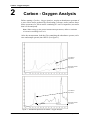
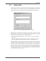
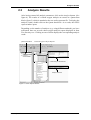
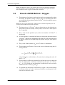
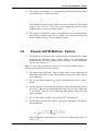
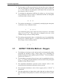
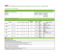
Version 6
User Manual
SEMI
© 2005 BRUKER OPTIK GmbH, Rudolf Plank Str. 27, D-76275 Ettlingen, www.brukeroptics.com
All rights reserved. No part of this manual may be reproduced or transmitted in any form or by any
means including printing, photocopying, microfilm, electronic systems etc. without our prior written permission. Brand names, registered trademarks etc. used in this manual, even if not explicitly marked as
such, are not to be considered unprotected by trademarks law. They are the property of their respective
owner.
The following publication has been worked out with utmost care. However, Bruker Optik GmbH does
not accept any liability for the correctness of the information. Bruker Optik GmbH reserves the right to
make changes to the products described in this manual without notice.
This manual is the original documentation for the OPUS spectroscopic software.
Table of Contents
1
Introduction . . . . . . . . . . . . . . . . . . . . . . . . . . . . . . . . . . . . . . . . . . . . . . . 1
2
Carbon - Oxygen Analysis . . . . . . . . . . . . . . . . . . . . . . . . . . . . . . . . . . . 2
2.1
2.2
2.3
3
Select Files . . . . . . . . . . . . . . . . . . . . . . . . . . . . . . . . . . . . . . . . . . . . . . . . . . . .3
Analysis Parameters . . . . . . . . . . . . . . . . . . . . . . . . . . . . . . . . . . . . . . . . . . . . .4
2.2.1
Oxygen / Carbon Methods . . . . . . . . . . . . . . . . . . . . . . . . . . . . . . . .4
2.2.2
Other Analysis Parameters . . . . . . . . . . . . . . . . . . . . . . . . . . . . . . . .6
Analysis Results . . . . . . . . . . . . . . . . . . . . . . . . . . . . . . . . . . . . . . . . . . . . . . . .7
Calculation Algorithms. . . . . . . . . . . . . . . . . . . . . . . . . . . . . . . . . . . . . . 8
3.1
3.2
3.3
3.4
3.5
3.6
3.7
3.8
3.9
3.10
3.11
Calculation of the Wafer Thickness . . . . . . . . . . . . . . . . . . . . . . . . . . . . . . . . .8
Ratio 1 Method - Oxygen . . . . . . . . . . . . . . . . . . . . . . . . . . . . . . . . . . . . . . . . .9
Ratio 2 Method - Oxygen . . . . . . . . . . . . . . . . . . . . . . . . . . . . . . . . . . . . . . . .10
Ratio Method - Carbon . . . . . . . . . . . . . . . . . . . . . . . . . . . . . . . . . . . . . . . . . .10
Pseudo ASTM Method - Oxygen . . . . . . . . . . . . . . . . . . . . . . . . . . . . . . . . . .12
Pseudo ASTM Method - Carbon . . . . . . . . . . . . . . . . . . . . . . . . . . . . . . . . . .13
ASTM F 1188-93a Method - Oxygen . . . . . . . . . . . . . . . . . . . . . . . . . . . . . .14
ASTM F 1391-92 Method - Carbon . . . . . . . . . . . . . . . . . . . . . . . . . . . . . . . .16
DIN 50438-1 A (93) Method - Oxygen . . . . . . . . . . . . . . . . . . . . . . . . . . . . .17
DIN 50438-1 B (93) Method - Oxygen . . . . . . . . . . . . . . . . . . . . . . . . . . . . .19
DIN 50438-2 (82) Method - Carbon. . . . . . . . . . . . . . . . . . . . . . . . . . . . . . . .22
Appendix . . . . . . . . . . . . . . . . . . . . . . . . . . . . . . . . . . . . . . . . . . . . . . . . 25
1
Introduction
The software package OPUS/SEMI is intended for analyses in the field of semiconductor quality control.
On the basis of an absorbance spectrum of a wafer, this OUS function calculates
the impurity concentration of interstitial oxygen (Oi) and substitutional carbon
(Cs) in silicon wafers.
OPUS/SEMI provides evaluation methods based on the following ASTM and
DIN standards:
•
•
•
•
•
ASTM F 1188-93a Oxygen
ASTM F 1391-92 Carbon
DIN 50438-1 A (93) Oxygen
DIN 50438-1 B (93) Oxygen
DIN 50438-2 (82) Carbon
Besides the evaluation methods based on the above listed ASTM and DIN standards, the following methods are available:
• The pseudo ASTM method which requires that the wafer thickness is
already known.
• The ratio method which automatically computes the wafer thickness
from the silicon matrix peaks.
• A special ratio method which is designed to deal with strongly
curved baselines which can occur when analyzing samples with a
rough surface and/or free charge carriers.
Note: For the calculation algorithms of the available evaluation methods refer to
chapter 3.
The CARBon-OXygen Analysis function of OPUS/SEMI is suited for two types
of wafers having different surface treatments:
• Double-side polished or polish-etched wafers
• Single-side polished wafers with etched back surfaces
Bruker Optik GmbH
OPUS/SEMI
1
Carbon - Oxygen Analysis
2
Carbon - Oxygen Analysis
Before starting a Carbon - Oxygen Analysis, acquire an absorbance spectrum of
a pure silicon wafer produced by float-zoning (reference wafer) and an absorbance spectrum of a silicon wafer containing Oi- and Cs-impurities (test wafer
that is to be analyzed).
Note: When setting up the general measurement parameters, define a resolution
of 4.0 and a zerofilling factor of 2.
After the measurement, load the files containing the absorbance spectra (reference and sample spectra) into OPUS. (See figure 1.)
Test Wafer
Spectrum
Reference Wafer
Spectrum
Test Wafer
Spectrum
Reference Wafer
Spectrum
Figure 1: Absorbance Spectra for the Carbon - Oxygen Analysis
2
OPUS/SEMI
Bruker Optik GmbH
Select Files
2.1
Select Files
To determine the impurity concentrations of interstitial oxygen (Oi) and substitutional carbon (Cs) in a silicon wafer, select in the OPUS Evaluate menu the
CARBon-OXygen Analysis function. The following dialog window appears:
Figure 2: Carbon-Oxygen Analysis Dialog Window - Select Files
Drag and drop the absorbance data block of the reference wafer in the upper
field Reference wafer spectrum and the absorbance data block(s) of the test
wafer(s) in the lower field File(s) for CARBOX analysis.
Note: The OPUS function CARBon - OXygen Analysis accepts only absorbance
data blocks.
Note: This OPUS function allows also the evaluation of a 3D data block (of the
test wafer). In this case, the concentrations Oi and Cs are displayed as traces.
Enter the thickness values (in mm) of the reference and the test wafer in the corresponding fields, provided that these values are known. For all evaluation
methods - except for RATIO Method 1 and RATIO Method 2 - the thickness values of the reference and the test wafer need to be entered. If the thickness is
unknown, enter the value 0. In this case, the thickness is calculated using the silicon phonon peak at 610cm-1. (The algorithm for the wafer thickness calculation is described in detail in chapter 3).
Bruker Optik GmbH
OPUS/SEMI
3
Carbon - Oxygen Analysis
2.2
Analysis Parameters
Click on the Analysis Parameter tab. The following dialog window appears:
Figure 3: Carbon-Oxygen Analysis Dialog Window - Analysis Parameters
2.2.1
Oxygen / Carbon Methods
In this dialog window, you specify the parameters for the carbon-oxygen analysis. The following evaluation methods are available:
•
•
•
•
•
•
•
ASTM F 1188-93a / ASTM F 1391-92
DIN 50438-1 A (93) / ASTM F 1391-92
DIN 50438-1 B (93) / ASTM F 1391-92
RATIO-Method 1
RATIO-Method 2
Pseudo ASTM
No Oxygen Analysis / DIN 50438-2 (82)
The methods for calculating the interstitial oxygen concentration are:
•
•
•
•
•
•
4
ASTM F 1188-93a
DIN 50438-1 A (93)
DIN 50438-1 B (93)
RATIO-Method 1
RATIO-Method 2
Pseudo ASTM
OPUS/SEMI
Bruker Optik GmbH
Analysis Parameters
The methods for calculating the substitutional carbon concentration are:
•
•
•
•
ASTM F 1391-92
RATIO-Method
Pseudo ASTM
DIN 50438-2 (82)
The RATIO - Methods 1 and 2 are suited for double-side polished wafers and
for wafers with a rough backside. Using these methods, the height of the oxygen
peak (at 1107cm-1) and the height of the carbon peak (at 605cm-1) are calculated for both spectra (i.e. the reference wafer spectrum and the test wafer spectrum). For this purpose, proper baselines are fitted. Then, a so-called ratio factor
is calculated using the silicon peak at 738cm-1. The oxygen and carbon peak
heights of reference wafer spectrum are multiplied with this ratio factor and
subtracted from the peak height of the test wafer spectrum. Using the corrected
peak heights, the software calculates the oxygen and carbon concentrations by
dividing these peak heights by the height of the baseline corrected silicon peak
at 617cm-1 of the test wafer spectrum and multiplying it by appropriate proportional factors.
In case of RATIO-Method 1, linear baselines are fitted, whereas in case of
RATIO-Method 2 a quadratic polynomial is used for the oxygen baseline. This
method can be used for spectra with a strong curved baseline.
The Pseudo ASTM Method can only be used for silicon slices polished on
both sides.
Taking the multiple reflections on both wafer surfaces into account, the formula
for calculating the transmittance spectrum (T=10-Absorbance) is:
2 – αd
1 – R) e
T = (-----------------------------2 – 2αd
1–R e
with d being the wafer thickness and R being the reflectivity (0.3). Using the
this formula, the absorption coefficient α is calculated.
The α-values for the peak and the baseline point are evaluated and then the
baseline value is subtracted from the peak value. This is done for both the reference wafer spectrum and the test wafer spectrum. Then, the α-values from the
reference measurement are subtracted from those of the test wafer spectrum.
These corrected α-values are proportional to the impurity concentrations.
Note: The complete calculation algorithms for all evaluation methods are
described in chapter 3.
If you are not sure which oxygen / carbon method you should use, select
ASTM F 1188-93a (oxygen) and ASTM F 1391-92 (carbon).
Bruker Optik GmbH
OPUS/SEMI
5
Carbon - Oxygen Analysis
2.2.2
Other Analysis Parameters
In the group field Units, specify the unit (ppm atomic or atoms/ccm) in which
the concentration values in the Quant report are to be displayed by clicking on
the corresponding option button.
In the group field Conversion Coefficients, specify the conversion coefficients
for oxygen and carbon. These conversion coefficients are multiplied by the
absorption coefficients for the oxygen peak and the carbon peak to get the concentration values. For the evaluation methods based on ASTM standards, the
default values of the conversion coefficients are: oxygen: 3.14 E17/cm and carbon: 0.82 E17/cm.
The multiplication factors Factor FO (oxygen) and Factor FC (carbon) have
the default value 1. If you measure calibration wafers with known oxygen and
carbon concentrations you can use these factors for your calibration.
In the group field Thickness Calculation you specify the Offset and the Slope.
The default parameters are only valid for double-side polished wafers and a certain thickness range (approx. from 0.3 to 2.5mm). If your wafer does not fulfill
the above mentioned conditions concering surface treatment and thickness, you
need to change these default values.
Note: It is better to work with known thickness values than to calculate them on
the basis of the FT-IR spectrum as described in chapter 3, section 3.1.
In case of the method DIN 50438-1 A (93), the concentration of the free charge
carriers needs to be entered as well. See figure 4.
Parameters of the
Charge Carrier
Concentration
Figure 4: Analysis Parameters of the Charge Carrier Concentration
6
OPUS/SEMI
Bruker Optik GmbH
Analysis Results
2.3
Analysis Results
After having entered all analysis parameters, click on the Analyze button. (See
figure 4.) The results of a carbon-oxygen analysis are stored in a Quant data
block (figure 5) which is attached to the test wafer spectrum file. To display the
analysis results, double-click on the Quant data block. As a result, the OPUS
report window opens.
Depending on the number of analyses (e.g. using different methods) you have
performed, there are several carbon oxygen analysis reports displayed in form
of a directory tree. Clicking on one of them displays the corresponding analysis
result.
Quant Data Block
Carbon Oxygen Analysis Reports
Used Analysis Parameters
Analysis Results
Figure 5: OPUS Report Window
Bruker Optik GmbH
OPUS/SEMI
7
Calculation Algorithms
3
Calculation Algorithms
This chapter describes the calculation algorithms of the different methods for
determining the oxygen and the carbon impurity concentrations.
3.1
Calculation of the Wafer Thickness
For the calculation of the wafer thickness, the silicon phonon peak at 610cm-1 in
the absorbance spectrum is used.
1) The absorption values of the three data points at the wavenumbers
617.18, 619.1 and 615.26cm-1 are averaged. (The data point nearest to
the specified wavenumber is chosen.)
Note: These data points are not exactly in the center of the peak, but slightly offcenter.
2) The baseline is a straight line calculated by fitting the six data points
(the data point at 651.9cm-1 and the two neighboring data points as well
as the data point at 576.68cm-1 and the two neighboring data points)
using the least-squares method.
3) The y-value of the baseline at 617.18cm-1 is determined.
4) This value is subtracted from the absorption value calculated in step 1.
The result is called AD.
5) The wafer thickness is calculated using the following empirical formula:
d[mm] = 0.02563 + 2.91474 • AD
with 0.02563 being the default Offset value and 2.91474 being the
default Slope value.
Note: This formula can only be used for double-side polished wafers having a
certain thickness range (approx. from 0.3 to 2.5mm).
For a more flexible thickness calculation, the parameters Offset (a) and
Slope (b) in the above formula are free parameters:
d[mm] = a + b • AD
8
OPUS/SEMI
Bruker Optik GmbH
Ratio 1 Method - Oxygen
3.2
Ratio 1 Method - Oxygen
1) The data point at 1107.08cm-1 and two data points on the right and two
data points on the left (totally 5 data points) are used for a least squares
fit to a parabola.
2) The y-value of this parabola (AP) at the wavenumber 1107.08cm-1 is
determined.
3) A linear baseline is calculated by fitting six data points (the data point at
1299.9cm-1 and two neighboring data points as well as the data point at
940cm-1 and two neighboring data points) using the least squares
method.
4) The y-value of the baseline (AB) at 1107.08cm-1 is determined.
5) The difference A P – A B for both the test wafer spectrum and the reference wafer spectrum are calculated. The results are AT (absorption value
of the test wafer spectrum) and AR (absorption value of the reference
wafer spectrum).
6) For the calculation of the so-called ratio factor (R), the silicon peak at
738cm-1 is used. The y-values of the data points at 740.6, 738.0 and
736.0cm-1 are averaged. The calculated average value ASIP is taken as
intensity of the peak maximum.
7) For the calculation of the baseline, five data points are used. The absorption value of the left baseline point (BL) is the mean value of the y-values at 1043.4, 1041.5 and 1039.6cm-1. The absorption value of the right
baseline point (BR) is the mean value of the y-values at 700 and
698cm-1. The value of the baseline (ASIB) at 738 cm-1 is calculated
using the following formula:
ASI B =
(BL • 40 + BR • 300)
340
8) The difference ASI P – ASI B for both the test wafer and the reference
wafer spectrum are calculated. The results are ASIT and ASIR.
9) The ratio factor R is calculated as follows:
R = ASI T
ASI R
10) The absorption value of oxygen (Ao) is calculated using the following
equation:
AO = AT - R • AR
Bruker Optik GmbH
OPUS/SEMI
9
Calculation Algorithms
11) The oxygen concentration co is calculated using the following formula:
A O • 3.14 • 17 - 2
-1
c O = 6.4 cm •
10 cm
AD
with AD being the absorption value (at 610cm-1,silicon peak) which has
been calculated in the course of the thickness calculation for the test
wafer spectrum (See section 3.1.) The factor 3.14 is the conversion coefficient (oxygen) which can be changed by the user in the CARBon-OXygen Analysis dialog window.
12) Then, the calculated oxygen concentration value is multiplied by the
factor FO (Factor Oxygen), which can be specified by the user:
C O = cO • FO
Note: The thickness value is not used for the oxygen concentration calculation.
Only the baseline corrected absorption value AD of the silicon peak at 610cm-1
has an influence on the oxygen concentration calculation.
3.3
Ratio 2 Method - Oxygen
The difference between Ratio 1 Method and Ratio 2 Method concerns only
step 3. For determining the absorption value of the baseline (AB), a parabola is
fitted.
A parabolic baseline is calculated by fitting the following 12 data points:
•
•
•
•
3.4
data point at 1299.9cm-1 and the two neighboring data points
data point at 1180cm-1 and the two neighboring data points
data point at 1040cm-1 and the two neighboring data points
data point at 940cm-1 and the two neighboring data points
Ratio Method - Carbon
1) The data point at 605.6cm-1 and two data points on the right and two
data points on the left (totally 5 data points) are used for a least squares
fit to a parabola.
2) The y-value of the parabola (AP) at the wavenumber 605.6cm-1 is determined.
3) A linear baseline is calculated by fitting six data points (the data point at
622.97cm-1 and the two neighboring data points as well as the data point
at 567.04cm-1 and the two neighboring data points) using the least
square method.
4) The y-value of the baseline (AB) at 605.6cm-1 is determined.
10
OPUS/SEMI
Bruker Optik GmbH
Ratio Method - Carbon
5) The difference A P – A B for both the test wafer spectrum and the reference wafer spectrum are calculated. The results are AT (absorption value
of the test wafer spectrum) and AR (absorption value of the reference
wafer spectrum).
6) For the calculation of the so-called ratio factor (R), the silicon peak at
738cm-1 is used. The y-values of the data points at 740.6, 738.0 and
736.0cm-1 are averaged. This average value ASIP is taken as intensity of
the peak maximum.
7) For the calculation of the baseline, five data points are used. The absorption value of the left baseline point (BL) is the average value of the yvalues at the wavenumbers 1043.4, 1041.5 and 1039.6cm-1. The absorption value of the right baseline point (BR) is the average value of the yvalues at the wavenumbers 700 and 698cm-1. The value the baseline
(ASIB) at 738cm-1 is calculated using the following formula:
ASI B =
(BL • 40 + BR • 300)
340
8) The difference ASI P – ASI B for both the test wafer spectrum and the
reference wafer spectrum are calculated. The results are ASIT and ASIR.
9) The ratio factor R is calculated as follows:
R = ASI T
ASI R
10) The absorption value of carbon (AC) is calculated using the following
equation:
AC = AT - R • AR
11) The carbon concentration cC is calculated using the formula:
AC • 8.2 • 16 - 2
-1
cC = 10.14 cm •
10 cm
AD
with AD being the absorption value (at 610cm-1, silicon peak) which has
been calculated in the course of the thickness calculation for the test
wafer spectrum. (See section 3.1.) The factor 8.2 is the conversion coefficient (carbon) which can be changed by the user in the CARBon-OXygen Analysis dialog window. The carbon concentration value is
multiplied by the factor FC, which can be specified by the user:
C C = cC • FC
Bruker Optik GmbH
OPUS/SEMI
11
Calculation Algorithms
Note: The thickness value is not used for the oxygen concentration calculation.
Only the baseline corrected absorbance value AD of the silicon peak at 610cm-1
has an influence on the oxygen concentration calculation.
3.5
Pseudo ASTM Method - Oxygen
1) The thickness of reference wafer and test wafer are determined by either
measuring the thickness using a caliper gauge or calculating the thickness using the silicon phonon peak at 610cm-1 in the absorbance spectra.
(See section 3.1.)
Note: First the oxygen absorption coefficients are calculated separately for test
wafer spectrum and reference wafer spectrum.
2) The data point at 1107.08cm-1 and two data points on the right and two
data points on the left (totally 5 data points) are used for a least squares
fit to a parabola.
3) The y-value of this parabola (AP) at the wavenumber 1107.08cm-1 is
determined.
4) A linear baseline is calculated by fitting six data points (the data point at
1299.9cm-1 and the two neighboring data points as well as the data point
at 940cm-1 and the two neighboring data points) using the least squares
method.
5) The y-value of the baseline (AB) at 1107.08cm-1 is determined.
6) The absorption coefficients α for AP and AB are calculated using the following formula:
1
d
α = - ln
2
4
- (1 - R ) + (1 - R ) + 4 T 2 R 2
2 T R2
with d being the wafer thickness, R (ratio factor) having the value 0.3
and T = 10-A.
7) The absorption coefficient calculated for the baseline point is subtracted
from the absorption coefficient calculated for the peak at 1107cm-1
(αP - αB). The results are net absorption coefficients for the test wafer
and the reference wafer (αT and αR).
8) To calculate the absorption coefficient for oxygen αO the net absorption
coefficient of the test wafer is subtracted from the net absorption coefficient of the reference wafer:
αO =αT - α R
12
OPUS/SEMI
Bruker Optik GmbH
Pseudo ASTM Method - Carbon
9) The oxygen concentration cO is calculated by multiplying the absorption
coefficient αO by a calibration factor:
cO = 3.14 • 10 cm α O
17
-2
This calibration factor is also called conversion coefficient. The default
value is 3.14 x 1017cm-2. This value can be changed by the user in the
CARBon-OXygen Analysis dialog window.
10) The oxygen concentration value cO (calculated in step 9) is multiplied by
the factor FO (default value FO=1), which can be specified by the user
in the CARBon-OXygen Analysis dialog window:
C O = cO • FO
3.6
Pseudo ASTM Method - Carbon
1) The thickness of reference wafer and test wafer are determined by either
measuring the thickness using a caliper gauge or by calculating the
thickness using the silicon phonon peak at 610cm-1 in the absorbance
spectra. (See section 3.1.)
Note: First the carbon absorption coefficients are calculated separately for test
wafer spectrum and reference wafer spectrum.
2) The data point at 605.6cm-1 and two data points on the right and two
data points on the left (totally 5 data points) are used for a least squares
fit to a parabola.
3) The y-value of the parabola (AP) at the wavenumber 605.6cm-1 is determined.
4) A linear baseline is calculated by fitting six data points (the data point at
622.97cm-1 and the two neighboring data points as well as the data point
at 567.04cm-1 and the two neighboring data points) using the least
squares method.
5) The y-value of the baseline (AB) at 605.6cm-1 is determined.
6) The absorption coefficients α for AP and AB are calculated using the following formula:
2
4
1 - (1 - R ) + (1 - R ) + 4 T 2 R 2
α = - ln
d
2 T R2
with d being the wafer thickness, R (ratio factor) having the value 0.3
and T = 10-A.
Bruker Optik GmbH
OPUS/SEMI
13
Calculation Algorithms
7) The absorption coefficient calculated for the baseline point is subtracted
from the absorption coefficient calculated for the peak (at 605cm-1)
αP - αB. The results are net absorption coefficients for the test wafer and
the reference wafer (αT and αR).
8) To calculate the absorption coefficient for carbon (αC), the net absorption coefficient of the test wafer is subtracted from the net absorption
coefficient of the reference wafer:
αC = αT - α R
9) The carbon concentration cC is calculated by multiplying the absorption
coefficient αC by a calibration factor:
cC = 8.2 • 10 cm α C
16
-2
This calibration factor is also called conversion coefficient. The default
value is 8.2 x 1016cm-2. This value can be changed by the user in the
CARBon-OXygen Analysis dialog window.
10) The carbon concentration value cC (calculated in step 9) is multiplied by
the factor FC (default value FC=1), which can be specified in the CARBon-OXygen Analysis dialog window:
C C = cC • FC
3.7
ASTM F 1188-93a Method - Oxygen
1) The thickness of reference wafer and test wafer are determined by either
measuring the thickness using a caliper gauge or by calculating the
thickness using the silicon phonon peak at 610cm-1 in the absorbance
spectra. (See section 3.1.)
2) The absorbance spectrum of the reference wafer is multiplied by the factor d m ⁄ d r (with dm being the thickness of the test wafer and dr being the
thickness of the reference wafer).
3) The normalized absorbance spectrum of the reference wafer is subtracted from the absorbance spectrum of the test wafer.
4) The maximum absorbance value of the oxygen peak at 1107cm-1 is
determined.
5) This data point plus two data points on the right and two data points on
the left (totally 5 data points) are used for a least squares fit to a parabola.
14
OPUS/SEMI
Bruker Optik GmbH
ASTM F 1188-93a Method - Oxygen
6) The wavenumber of the parabola vertex vmax and the corresponding
absorption value AP are determined.
7) On the basis of the spectrum calculated in step 3, a linear baseline is calculated by fitting data points in the regions from 900 to 1000cm-1 and
from 1200 to 1300cm-1 using the least squares method.
8) The absorption value of the baseline AB at the wavenumber vmax is
determined.
9) The transmittance values, which correspond to the absorbance values AP
and AB, are calculated:
T P = 10
- AP
T B = 10
- AB
10) The absorption coefficients αP and αB for the peak maximum and the
baseline point are calculated using the following formula:
2
1 (0.09 - e1.7d ) + (0.09 - e1.7d ) + 0.36 T 2 e1.7d
α = - ln
0.18 T
d
with d being the thickness of the test wafer.
11) The absorption coefficient for oxygen αO is calculated:
αO=α P -α B
12) The oxygen concentration cO is calculated by multiplying the absorption
coefficient αO by a calibration factor (IOC-88):
cO = 3.14 • 10 cm α O
17
-2
This calibration factor is also called conversion coefficient. The default
value is 3.14 x 1017cm-1. This value can be changed by the user in the
CARBon-OXygen Analysis dialog window.
13) The oxygen concentration value cO is multiplied by the factor FO
(default value FO=1), which can be specified by the user in the
CARBon-OXygen Analysis dialog window.
C O = cO • FO
Bruker Optik GmbH
OPUS/SEMI
15
Calculation Algorithms
3.8
ASTM F 1391-92 Method - Carbon
1) The thickness of reference wafer and test wafer are determined by either
measuring the thickness using a caliper gauge or by calculating the
thickness using the silicon phonon peak at 610cm-1 in the absorbance
spectra. (See section 3.1.)
2) The absorbance spectrum of the reference wafer is multiplied by the factor d m ⁄ d r (with dm being the thickness of the test wafer and dr being the
thickness of the reference wafer).
3) The normalized absorbance spectrum of the reference wafer is subtracted from the absorbance spectrum of the test wafer.
4) The maximum absorbance value of the carbon peak at 605cm-1 is determined.
5) This data point plus two data points on the right and two data points on
the left (totally 5 data points) are used for a least squares fit to a parabola.
6) The wavenumber of the parabola vertex vmax and the corresponding
absorption value AP are determined.
7) On the basis of the spectrum calculated in step 3, a linear baseline is calculated by fitting data points in the regions from 550 to 570cm-1 and
from 630 to 650cm-1 using the least squares method.
8) The absorption value of the baseline AB at the wavenumber vmax is
determined.
9) The absorption coefficient for carbon αC is calculated using the following formula:
αC =
23.03
( AP - AB )
d
with d being the thickness of the test wafer.
10) The carbon concentration cC is calculated by multiplying the absorption
coefficient αC by a calibration factor:
cC = 8.2 • 10 cm α C
16
-2
This calibration factor is also called conversion coefficient. The default
value is 8.2 x 1016cm-2. This value can be changed by the user in the
CARBon-OXygen Analysis dialog window.
16
OPUS/SEMI
Bruker Optik GmbH
DIN 50438-1 A (93) Method - Oxygen
Note: The conversion coefficient (0.82 x 1017cm-2) is valid for spectra acquired
at room temperature. But this method can also be used for spectra acquired at
cryogenic temperatures (below 80 K). In this case, the absorption band peak is at
607.5cm-1 and the recommended conversion coefficient is 0.37 x 1017cm-2.
11) The carbon concentration value cC is multiplied by the factor FC (default
value FC=1) which can be specified by the user in the CARBon-OXygen
Analysis dialog window.
C C = cC • FC
3.9
DIN 50438-1 A (93) Method - Oxygen
1) The thickness of reference wafer and test wafer are determined by either
measuring the thickness using a caliper gauge or by calculating the
thickness using the silicon phonon peak at 610cm-1 in the absorbance
spectra. (See section 3.1.)
2) The absorbance spectrum of the reference wafer is multiplied by the factor d m ⁄ d r (with dm being the thickness of the test wafer and dr being the
thickness of the reference wafer).
3) The absorbance spectra are converted into transmittance spectra
(Tr = 10-Abs).
4) A so-called comparison spectrum is calculated by dividing the test wafer
spectrum by the reference wafer spectrum.
5) The minimum transmittance value of the oxygen peak at 1107cm-1 is
determined.
6) This data point plus two data points on the right and two data points on
the left (totally 5 data points) are used for a least squares fit to a parabola.
7) The wavenumber of the parabola vertex vmin and the corresponding
transmittance value TM are determined.
8) On the basis of the spectrum calculated in step 4, a linear baseline is calculated by fitting data points in the regions from 1025 to 1040cm-1 and
from 1180 to 1195cm-1 using the least squares method.
9) The transmittance value of the baseline TB at the wavenumber vmin is
determined.
10) The absorption coefficient for oxygen aO is calculated using the following formula:
Bruker Optik GmbH
OPUS/SEMI
17
Calculation Algorithms
αO=
- ln ( A + A2 + B 2 )
d
with:
A = T B ( 1 - B2 )
2TM
B=
1
exp( αd)
R
α = α A = α phon + α N
α phon = 0.85 cm-1
p - Si : α N = 1.43 • 10 -16 cm2 N(p)
n - Si : α N = 0.32 • 10 -16 cm2 N(n)
with N(n) and N(p) being the free charge carrier concentrations for pand n-type silicon.
11) The oxygen concentration cO is calculated by multiplying the absorption
coefficient αO by a calibration factor:
cO = 3.14 • 10 cm α O
17
-2
This calibration factor is also called conversion coefficient. The default
value is 3.14 x 1017cm-2. This value can be changed by the user in the
CARBon-OXygen Analysis dialog window.
12) The concentration value cO is multiplied by the factor FO, which can be
specified by the user in the CARBon-OXygen Analysis dialog window:
C O = cO • FO
18
OPUS/SEMI
Bruker Optik GmbH
DIN 50438-1 B (93) Method - Oxygen
3.10
DIN 50438-1 B (93) Method - Oxygen
1) The thickness of reference wafer and test wafer are determined by either
measuring the thickness using a caliper gauge or by calculating the
thickness using the silicon phonon peak at 610cm-1 in the absorbance
spectra. (See section 3.1.)
2) The absorbance spectrum of the reference wafer is multiplied by the factor d m ⁄ d r (with dm being the thickness of the test wafer and dr being the
thickness of the reference wafer).
3) The absorbance spectra are converted into transmittance spectra
(Tr = 10-Abs).
After that, the leveled transmittance spectrum of the test wafer is calculated as
follows:
4)
Θ a is the transmittance value at 1107cm-1 of curve a in figure 6.
5) This spectrum (curve a in figure 6) is leveled linearly in such a way that
the transmittances values at the wavenumbers 1200cm-1 and 1025cm-1
are identical. (See curve b in figure 6).
6)
Θ b is the transmittance value at 1107cm-1 of the linearly leveled spectrum. (See curve b in figure 6).
7) The linearly leveled spectrum (curve b in figure 6) is multiplied by
Θ a ⁄ Θ b . The result is the leveled spectrum. (See curve c in figure 6).
Figure 6: Leveling the Spectrum of a single-side polished Test Wafer
(Source: DIN 50438-1: Prüfung von Materialien für die Halbleitertechnologie - Bestimmung des
Verunreinigungsgehaltes in Silicium mittels Infrarot-Absorption - Teil 1, Berlin: Beuth Verlag
GmbH (1995-07).
Bruker Optik GmbH
OPUS/SEMI
19
Calculation Algorithms
8)
Θ t is the transmittance value at 1188cm-1 of the leveled spectrum. (See
curve c in figure 6).
After that, the adjusted transmittance spectrum of the reference wafer is calculated as follows:
9) The transmittance value Θ r at 1188cm-1 in the reference spectrum is
determined. This value has been corrected for thickness (step 2 and 3).
10) This spectrum is multiplied by the factor Θ t ⁄ Θ r . The result is an
adjusted transmittance spectrum.
11) Θ R is the transmittance value at 1107cm-1. This value is required for the
calculation of absorption coefficient αB. (See step 13.)
12) The leveled test wafer spectrum (curve c in figure 6) is divided by the
adjusted reference wafer spectrum to obtain the comparison spectrum T.
13) The absorption coefficient αB is calculated using the following formula:
αB=
- ln ( D + D 2 + 11.111 )
d
with d being the thickness of the test wafer. The parameter D is calculated as follows:
D=
- 2.722
ΘR
Using the comparison spectrum T, the values TM and TB are calculated as follows:
14) The minimum transmittance value of the oxygen peak at 1107cm-1 is
determined.
15) This data point plus two data points on the right and two data points on
the left (totally 5 data points) are used for a least squares fit to a parabola.
16) The wavenumber of the parabola vertex vmin and the corresponding
intensity value TM are determined.
17) A linear baseline is calculated by fitting data points in the regions from
1025 to 1040cm-1 and from 1180 to 1195cm-1 using the least squares
method.
18) The transmittance value of the baseline TB at the wavenumber vmin is
determined.
20
OPUS/SEMI
Bruker Optik GmbH
DIN 50438-1 B (93) Method - Oxygen
19) The absorption coefficient for oxygen αO is calculated using the following formula:
αO=
- ln ( A + A2 + B 2 )
d
with:
A = T B ( 1 - B2 )
2TM
B=
1
exp( α B d)
R
with αB being the absorption coefficient which has been calculated in
step 13 and d being the thickness of the test wafer.
20) The oxygen concentration is calculated by multiplying the absorption
coefficient cO by the calibration factor:
cO = 3.14 • 10 cm α O
17
-2
This calibration factor is also called conversion coefficient. The default
value is 3.14 x 1017cm-2. This value can be changed by the user in the
CARBon-OXygen Analysis dialog window.
21) The oxygen concentration value is multiplied by the factor FO which
can be specified by the user in the CARBon-OXygen Analysis dialog
window:
C O = cO • FO
Bruker Optik GmbH
OPUS/SEMI
21
Calculation Algorithms
3.11
DIN 50438-2 (82) Method - Carbon
1) The thickness of reference wafer and test wafer are determined by either
measuring the thickness using a caliper gauge or by calculating the
thickness using the silicon phonon peak at 610cm-1 in the absorbance
spectra. (See section 3.1.)
2) The absorbance spectrum of the reference wafer is multiplied by the factor d m ⁄ d r (with dm being the thickness of the test wafer and dr being the
thickness of the reference wafer).
3) The absorbance spectra are converted into transmittance spectra
(Tr = 10-Abs).
4) A so-called comparison spectrum is calculated by dividing the test wafer
spectrum by the reference wafer spectrum.
5) The minimum transmittance value of the carbon peak at 605cm-1 is
determined (provided that the spectrum has been acquired at room temperature).
Note: In case the spectrum has been acquired at cryogenic temperatures, the minimum transmittance value of the carbon peak at 607.5cm-1 is determined.
6) This data point plus two data points on the right and two data points on
the left (totally 5 data points) are used for a least squares fit to a parabola.
7) The wavenumber of the parabola vertex vmin and the corresponding
transmittance value TM are determined.
8) The baseline is constructed as a tangent to the comparison spectrum in
such a way that the spectrum contacts it at least at one point on each side
of the absorption band, but it is not cut at any point.
9) The transmittance value of the baseline TB at the wavenumber vmin is
determined.
10) The absorption coefficient for carbon αC is calculated using the following formula:
αc=
ln ( T B / T M )
d
11) The carbon concentration cc is calculated by multiplying the absorption
coefficient αC by a calibration factor:
cc = 1.0 • 10 cm α c
17
22
OPUS/SEMI
-2
Bruker Optik GmbH
DIN 50438-2 (82) Method - Carbon
This calibration factor is also called conversion coefficient. The default
value is 1.0 x 1017cm-2. This value can be changed by the user in the
CARBon-OXygen Analysis dialog window.
Note: The conversion coefficient (1.0 x 1017cm-2) is valid for spectra acquired at
room temperature. But this method can also be used for spectra acquired at cryogenic temperatures (below 80 K). In this case, the absorption band peak is at
607.5cm-1 and the recommended conversion coefficient is 0.45 x 1017cm-2.
12) The concentration value cc is multiplied by the factor FC, which can be
specified by the user in the CARBon-OXygen Analysis dialog window:
C c = cc • FC
Bruker Optik GmbH
OPUS/SEMI
23
Calculation Algorithms
24
OPUS/SEMI
Bruker Optik GmbH
Appendix
ASTM and DIN Standards
As already mentioned in chapter 1, the OPUS/SEMI software supports the following ASTM and DIN standards:
•
•
•
•
•
ASTM F 1188-93a Oxygen
ASTM F 1391-92 Carbon
DIN 50438-1 A (93) Oxygen
DIN 50438-1 B (93) Carbon
DIN 50438-2 (82) Carbon
It is highly recommended to purchase these standards. You can order them, for
example, at the Beuth Verlag GmbH (www.beuth.de) or at ASTM International
(www.astm.org). This appendix quotes the scope or range of application and
purpose of the following standards:
•
•
•
•
ASTM F 1188-93a
ASTM F 1391-92
DIN 50438-1
DIN 50438-2 (82)
ASTM F 1188-93a1
Standard Test Method for Interstitial Atomic Oxygen Content of Silicon by
Infrared Absorption
1. Scope
1.1 This test method covers the determination of the interstitial oxygen content
of single crystal silicon by infrared spectroscopy. This test method requires the
use of an oxygen-free reference specimen. (...)
1.2 The useful range of oxygen concentration measurable by this test method is
from 1 x 10¹⁶ atoms/cm3 to the maximum amount of interstitial oxygen soluble
in silicon.
1.3 The oxygen concentration obtained using this test method assumes a linear
relationship between the interstitial oxygen concentration and the absorption
coefficient of the 1107cm-1 band associated with interstitial oxygen in silicon.
1.4 (...)
1. ASTM F 1188-93a (Published 1993): Standard Test Method for Interstitial Atomic Oxygen Content of
Silicon by Infrared Absorption. ASTM International, West Conshohocken, Pennsylvania, U.S.
Bruker Optik GmbH
OPUS SEMI
25
Appendix
ASTM F 1391-921
Standard Test Method for Substitutional Atomic Carbon Content of Silicon by Infrared Absorption
1. Scope
1.1 This referee test method covers the determination of substitutional carbon
concentration in single crystal silicon. Because carbon may also reside in interstitial lattice positions, when in concentrations near the solid solubility limit, the
result of this test method may not be a measure of the total carbon concentration.
1.2 The useful range of carbon concentration measurable by this test method is
from the maximum amount of substitutional carbon soluble in silicon down to
about 0.1 parts per million atomic (ppma), that is, 5 x 1015cm-3 for measurements at room temperature, and down to about 0.01 ppma, that is, 0.5 x 10¹⁵
cm-3 at cryogenic temperatures (below 80 K).
1.3 This test method utilizes the relationship between carbon concentration and
the absorption coefficient of the infrared absorption band associated with substitutional carbon in silicon. At room temperatures (about 300 K), the absorption band peak is at 605cm-1 or 16.53µm. At cryogenic temperatures (below 80
K), the absorption band peak is at 607.5cm-1 or 16.46µm.
1.4 This test method is applicable to slices of silicon with a resistivity higher
than 3Ω-cm for p-type and higher than 1Ω-cm for n-type. Slices an be any crystallographic orientation and should be polished on both surfaces.
1.5 This method is intended to be used infrared spectrophotometers that operate
in the region from 2000 to 500cm-1 (5 - 20µm).
1.6 This test method provides procedure and calculation sections for the cases
where the thickness values of test and reference specimens are both closely
matched and not closely matched.
1.7 (...)
1.ASTM F 1391-92 (Published 1992): Standard Test Method for Substitutional Atomic Carbon Content
of Silicon by Infrared Absorption. ASTM International, West Conshohocken, Pennsylvania, U.S.
26
OPUS SEMI
Bruker Optik GmbH
DIN 50438, Part 11
Testing of Materials for Semiconductor Technology: Determination of
Impurity Content in Semiconductors by Infrared Absorption - Part 1:
Oxygen
1. Range of Application and Purpose
The Methods A and B of this standard serve to determine with high precision
the oxygen content of silicon by non-destructive optical infrared means. Only
the interstitial oxygen content of the silicon is detected by these methods. The
total oxygen content may be greater than the interstitial oxygen content. (...)
The range of application of the methods is limited to plane-parallel mono- or
polycrystalline silicon wafers with thicknesses d > 0.03 cm and charged carrier
16
concentrations N ≤ 2x10 cm-3, and is independent of crystal orientation. The
methods are applicable to both of the currently used types of specimens having
different surface treatments and thicknesses:
• Double-side polished or polish-etched wafers with a thickness
d ≥ 0, 006 cm (Method A)
• One-side-polished wafers with etched back surfaces and thicknesses
d ≥ 0, 003 cm (Method B)
Specimens having only sawed or only lapped surfaces do not fulfill the requirements of this standard.
The measurement range for oxygen concentration lies between
co = 2.5 x 1015cm-3 and the solubility of oxygen of about 2.5 x 1018cm-3 at the
melting point of silicon. (...)
1.DIN 50438, Part 1 (1993): Testing of Materials for Semiconductor Technology Determination of Impurity Content in Semiconductors by Infrared Absorption Oxygen in Silicon. Berlin: Beuth Verlag GmbH.
Bruker Optik GmbH
OPUS SEMI
27
Appendix
DIN 50438, Part 21
Testing Materials for Semiconductor Technology: Determination of Impurity Content in Silicon Using Infrared Absorption - Part 2: Carbon
1. Range of Application and Purpose
The process, according to this standard, is used to determine the carbon content
of silicon. The absorption coefficient of substitutional carbon at a wave number
of 605 cm-1 (16.5µm - absorption band) is used to measure carbon content.
Therefore, this procedure does not apply to carbon that may be present in
another form in the silicon lattice or chemically linked or is precipitated at gain
boundaries or other places. With this limitation, the application range of the
procedure covers plane-parallel, two-sided polished test pieces of single-crystal
or polycrystalline silicon with charge carrier concentrations under 5 x 1016cm-3,
regardless of conductivity type and crystal orientation. The measurement range
for the carbon concentration lies between 5 x 1015cm-3 and about 3 x 1018cm-3.
Due to the strong silicon lattice absorption (absorption coefficient KG ≈ 8cm-1
for wave number 605 cm-1 (2)), that is superimposed on the (605cm-1) band
generated by the carbon, the carbon content can only be determined using a differential process.
1.DIN 50438, Part 2 (1982): Testing of Materials for Semiconductor Technology: Determination of Impurity Content in Silicon Using Infrared Absorption - Carbon. Berlin: Beuth Verlag GmbH.
28
OPUS SEMI
Bruker Optik GmbH
Index
Ratio method 1, 4, 5
A
Single-side polished wafer 1, 19
Slope 6, 8
Substitutional carbon 1, 3, 5, 26, 28
Absorption coefficient 5, 6, 12, 13, 14, 15,
17, 18, 20, 21, 22, 25, 26, 28
ASTM F 1188-93a 1, 4, 5, 14, 25
ASTM F 1391-92 1, 4, 5, 16, 25, 26
S
T
Two-sided polished test pieces 28
C
W
Calibration factor 13, 14, 15, 16, 18, 21, 22,
23
Charge carrier concentration 6, 18, 28
Conversion coefficient 6, 10, 11, 13, 14, 15,
16, 17, 18, 21, 23
Wafer thickness 1, 3, 5, 8, 12, 13
D
DIN 50438-1 2, 27
DIN 50438-1 A (93) 1, 4, 6, 17
DIN 50438-1 B (93) 1, 4, 19
DIN 50438-2 1, 4, 22, 25, 28
Double-side polished wafer 1, 5, 27
F
FC factor 6, 11, 14, 17, 23
FO factor 6, 10, 13, 15, 18, 21
I
Interstitial oxygen 1, 3, 4, 25, 27
O
Offset 6, 8
One side-polished wafer 27
P
Polish-etched wafer 1, 27
Pseudo ASTM method 1, 4, 5, 12, 13
Q
Quant data block 7
Quant report 6
R
Ratio 1 method 9
Ratio 2 method 10
Ratio factor 5, 9, 11, 12, 13