1
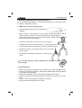
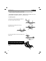
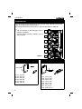
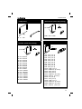
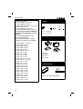
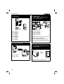
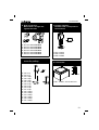
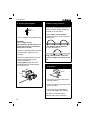
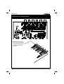
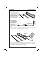
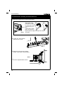
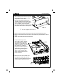
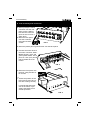
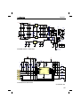
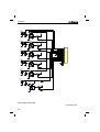
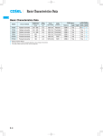
Total solder points: 500
Difficulty level:
beginner 1o 2o 3o 4o 5þ advanced
HIGH-END CONTROL AMPLIFIER
K8021
ILLUSTRATED ASSEMBLY MANUAL
H8021IP-1
VELLEMAN KIT NV
Legen Heirweg 33
9890 Gavere
Belgium
http://www.velleman.be
Assembly hints
1. Assembly (Skipping this can lead to troubles ! )
Ok, so we have your attention. These hints will help you to make this project
successful. Read them carefully.
1.1 Make sure you have the right tools:
• A good quality soldering iron (25-40W) with a
small tip.
• Wipe it often on a wet sponge or cloth, to keep it clean; then apply solder to
the tip, to give it a wet look. This is called ‘thinning’ and will protect
the tip, and enables you to make good connections. When solder
rolls off the tip, it needs cleaning.
• Thin raisin-core solder. Do not use any flux or grease.
• A diagonal cutter to trim excess wires. To avoid injury when cutting
excess leads, hold the lead so they cannot fly towards the eyes.
• Needle nose pliers, for bending leads, or to hold components in place.
• Small blade and phillips screwdrivers. A basic range
is fine.
For some projects, a basic multi-meter is required, or might
be handy
0.0
00
1.2 Assembly Hints :
⇒ Make sure the skill level matches your experience, to avoid disappointments.
⇒ Follow the instructions carefully. Read and understand the entire step before
you perform each operation.
⇒ Perform the assembly in the correct order as stated in this manual
⇒ Position all parts on the PCB (Printed Circuit Board) as shown on the drawings.
⇒ Values on the circuit diagram are subject to changes.
⇒ Values in this assembly guide are correct*
3
Assembly hints
⇒ Use the check-boxes to mark your progress.
⇒ Please read the included information on safety and customer service
* Typographical inaccuracies excluded. Always look for possible last minute
manual updates, indicated as ‘NOTE’ on a separate leaflet.
1.3 Soldering Hints :
1- Mount the component against the PCB surface and carefully solder the leads
2- Make sure the solder joints are coneshaped and shiny
3- Trim excess leads as close as possible to the
solder joint
AXIAL COMPONENTS ARE TAPED IN
THE CORRECT MOUNTING SEQUENCE !
REMOVE THEM FROM THE TAPE ONE AT A
TIME !
4
P
E
Aran-
Giallo
Verde
Blu
Viola
Grigio
Bianco
3
4
5
6
7
8
9
Naran-
Oranssi
Brun
Svart
Orange
Blå
Grön
Kulta
B Oro
Dourado Oro
Grå
Guld
Silver
Valkoinen Vit
Hopea
Blanco
Harmaa
A Argento Prateado Plata
Branco
Sininen
Vihreä
Morado Purppura Lila
Azul
Verde
Cinzento Gris
Violeta
Azul
Verde
S
DK
4K7= ( 4 - 7 - 0 - 1 - 1 )
1%
N
Rød
Brun
Sort
Guld
Sølv
Hvid
Grå
Violet
Blå
Grøn
Gul
Guldl
Sølv
Hvidt
Grå
Violet
Blå
Grønn
Gul
Orange Orange
Rød
Brun
Sort
FÄRG FARVE- FARGESCHEMA KODE
KODE
Punainen Röd
Ruskea
Musta
VÄRI
KOODI
SF
Amarelo Amarillo Keltainen Gul
Laranja
Rojo
Rosso
2
Encar-
Marrone Castanho Marrón
Negro
1
Preto
Nero
0
C CODICE CODIGO CODIGO
O COLORE
DE
DE
D
CORES COLORE
E
S
I
4K7= ( 4 - 7 - 2 - B )
5%
GB
F
NL
Gold
Silber
Weiss
Grau
Violet
Blau
Grün
Gelb
Orange
Rot
Braun
Gold
Silver
White
Grey
Purple
Blue
Green
Yellow
Orange
Red
Brown
Schwarz Black
Or
Argent
Blanc
Gris
Violet
Blue
Vert
Jaune
Orange
Rouge
Brun
Noir
2
1
0
4
Goud
Zilver
Wit
Grijs
B
A
9
8
Paars 7
Blauw 6
Groen 5
Geel
Oranje 3
Rood
Bruin
Zwart
FARB COLOUR CODIFI- KLEUR C
KODE
CODE CATION KODE O
D
DES
E
COU-
D
COLOR= 2… 5
Color code table
5
Construction
CONSTRUCTION
The unit consists out of two PCB’s, one is the main PCB, P8021B and the other
is the left channel input section P8021L.
First we will start with the small P8021L, then we assemble the P8021B.
FTip: The pictures on the packaging can be
used as a guideline.
However, due to possible changes it is not
100% reliable.
P8021L
1. Diodes (check the polarity)
2. Resistors (check the color code)
D...
CATHODE
q
q
q
q
q
q
6
D1: 1N4148
D2: 1N4148
D3: 1N4148
D4: 1N4148
D5: 1N4148
D6: 1N4148
R...
q
q
q
q
q
q
q
q
R1: 10K (1-0-3)
R2: 10K (1-0-3)
R3: 10K (1-0-3)
R4: 10K (1-0-3)
R5: 10K 1-0-3)
R6: 10K (1-0-3)
R7: 1K (1-0-2)
R8: 330R (3-3-1)
Construction
3. Capacitors
6. RCA connectors.
Mount them straight and
against the PCB
C...
q
q
q
q
q
q
C1: 220p (221)
C2: 220p (221)
C3: 220p (221)
C4: 220p (221)
C5: 220p (221)
C6: 220p (221)
4- Reed relays (check the position
q
q
q
q
q
q
SK1: MJ-523AG/B BLACK
SK2: MJ-523AG/B BLACK
SK3: MJ-523AG/B BLACK
SK4: MJ-523AG/B BLACK
SK5: MJ-523AG/B BLACK
SK6: MJ-523AG/B BLACK
of the notch)
7. Pin connector. Mount it exactly
as indicated
RY...
q
q
q
q
q
q
RY1: VR05051AS or eq.
RY2: VR05051AS or eq
RY3: VR05051AS or eq
RY4: VR05051AS or eq
RY5: VR05051AS or eq
RY6: VR05051AS or eq.
5. transistors
q SK7: HDR20/26
q
q
q
q
q
q
T1: BC557
T2: BC557
T3: BC557
T4: BC557
T5: BC557
T6: BC557
7
Construction
P8021B Assembly
8
Construction
1. Jump wires
3. Zener diode (check the polarity)
ZD...
CATHODE
q ZD1: 20V / 0.6W
q J1... J25
4. Resistors (check the color code)
2. Diodes (check the polarity)
D...
R...
CATHODE
q
q
q
q
q
q
q
q
q
q
q
q
q
q
q
q
D1: 1N4148
D2: 1N4148
D3: 1N4148
D4: 1N4148
D5: 1N4148
D6: 1N4148
D7: 1N4148
D8: 1N4148
D9: 1N4007
D10: 1N4007
D11: 1N4007
D12: 1N4007
D13: 1N4007
D14: 1N4007
D15: 1N4007
D16: 1N4007
q
q
q
q
q
q
q
q
q
q
q
q
q
q
q
q
q
q
q
q
q
R1: 10K (1-0-3)
R2: 10K (1-0-3)
R3: 10K (1-0-3)
R4: 10K (1-0-3)
R5: 10K (1-0-3)
R6: 10K (1-0-3)
R7: 10K (1-0-3)
R8: 10K (1-0-3)
R9: 47K (4-7-3)
R10: 470R (4-7-1)
R11: 620R/1% (6-2-0-0)
R12: 33R (3-3-0)
R13: 33R (3-3-0)
R14: 390K/1% (3-9-0-3)
R15: 33K/1% (3-3-0-2)
R16: 1K (1-0-2)
R17: 47K (4-7-3)
R18: 470R (4-7-1)
R19: 620R/1% (6-2-0-0)
R20: 390K/1% (3-9-0-3)
R21: 33K/1% (3-3-0-2)
9
Construction
q R22: 1K (1-0-2)
q R23: 560R/1% (5-6-0-0)
q R24: 1K8/1% (1-8-0-1)
q R25A or R25B: 1K5 (1-5-0-1) (*)
q R26: 1K5 (1-5-2)
q R27: 560R/1% (5-6-0-0)
q R28A or R28B: 1K5 (1-5-2) (*)
* The position of R25 and R28 depends on the supplied IC for IC2
and IC3:
Mount R25B and R28B if type
OPA134 is supplied.
Mount R25A and R28A. If types
OPA604 or TLE2071 are supplied.
q
q
q
q
q
q
q
q
q
q
q
q
q
q
q
q
q
q
q
q
q
q
q
q
q
10
R29: 1K8/1% (1-8-0-1)
R30: 1K5 (1-5-2)
R31: 56R (5-6-0)
R32: 56R (5-6-0)
R33: 1K (1-0-2)
R34: 330R (3-3-1)
R35: 1R (1-0-0)
R36: 1R (1-0-0)
R37: 1R (1-0-0)
R38: 1R (1-0-0)
R39: 1K/1% (1-0-0-1)
R40: 1K/1% (1-0-0-1)
R41: 1K (1-0-2)
R42: 1K (1-0-2)
R43: 1K (1-0-2)
R44: 1K (1-0-2)
R45: 10K (1-0-3)
R46: 10K (1-0-3)
R47: 10K (1-0-3)
R48: 10K (1-0-3)
R49: 10K (1-0-3)
R50: 4K7 (4-7-2)
R51: 1R (1-0-0)
R52: 470R (4-7-1)
R53: 1K5 (1-5-2)
5. Choke
L...
L...
q L1: 1uH (1-0)
q L2: 1uH (1-0)
6. IC sockets
q
q
q
q
IC1: 8P
IC2: 8P
IC3: 8P
IC4: 18P
7. Female header
SK..
J...
q SK7: 20P (type 96120205)
Construction
8. Capacitors
9. Reed relays (check the position
of the notch)
C...
RY...
q
q
q
q
q
q
q
q
q
q
q
q
q
q
q
q
q
q
q
q
q
q
q
q
q
q
q
q
q
q
q
C1: 220p (221)
C2: 220p (221)
C3: 220p (221)
C4: 220p (221)
C5: 220p (221)
C6: 220p (221)
C7: 220p (221)
C8: 220p (221)
C9: 220p (221)
C10: 2n2 (222, 2200)
C11: 2n2 (222, 2200)
C12: 8n2 (822, 8200)
C13: 8n2 (822, 8200)
C14: 100n (104, 0.1, u1)
C15: 100n (104, 0.1, u1)
C16: 100n (104, 0.1, u1)
C17: 100n (104, 0.1, u1)
C18: 100n (104, 0.1, u1)
C19: 100n (104, 0.1, u1)
C20: 100n (104, 0.1, u1)
C21: 100n (104, 0.1, u1)
C22: 100n (104, 0.1, u1)
C23: 100n (104, 0.1, u1)
C24: 100n (104, 0.1, u1)
C25: 100n (104, 0.1, u1)
C26: 100n (104, 0.1, u1)
C27: 100n (104, 0.1, u1)
C28: 100n (104, 0.1, u1)
C29: 100n (104, 0.1, u1)
C30: 2.2uF
C31: 2.2uF
q
q
q
q
q
q
q
q
RY1: VR05051AS or eq.
RY2: VR05051AS or eq
RY3: VR05051AS or eq
RY4: VR05051AS or eq
RY5: VR05051AS or eq
RY6: VR05051AS or eq.
RY7: VR05051AS or eq.
RY8: VR05051AS or eq.
10. Pin header connector, cut at
the indicated 5 pins
5
q SK8: 5P
q SK9: 5P
11
Construction
11. transistors
q
q
q
q
q
q
q
q
T1: BC557
T2: BC557
T3: BC557
T4: BC557
T5: BC557
T6: BC557
T7: BC557
T8: BC557
13. Push button
Mount them straight against
the PCB surface !
q
q
q
q
q
SW1: TS-04PV
SW2: TS-04PV
SW3: TS-04PV
SW4: TS-04PV
SW5: TS-04PV
Remark: The metal part of these buttons are used as jump wire.
Be sure not to test or use the unit
without soldering these push buttons.
12. Trim potentiometer
14. Phone jack.
Mount him straight against the
PCB surface !
L'
SK..
q RV1: 100K
q RV2: 100K
J...
q SK13: JCF3.5 (3.5mm jack)
12
R
R'
L
Construction
15. RCA connectors.
Mount them straight and
against the PCB
17. Voltage regulator.
The back side corresponds to
the thick line.
VR...
q
q
q
q
q
q
SK1: MJ-523AG/R RED
SK2: MJ-523AG/R RED
SK3: MJ-523AG/R RED
SK4: MJ-523AG/R RED
SK5: MJ-523AG/R RED
SK6: MJ-523AG/R RED
q VR1 UA7815
q VR2 UA7915
q VR3 UA7805
16. Electrolytic capacitors.
Check the polarity !
18. Transformer.
C...
q
q
q
q
q
q
q
q
q
q
q
q
q
q
q
q
C32: 47µ
C33: 47µ
C34: 100µ
C35: 100µ
C36: 100µ
C37: 470µ
C38: 470µ
C39: 470µ
C40: 470µ
C41: 470µ
C42: 1000µ
C43: 1000µ
C44: 1000µ
C45: 1000µ
C46: 1000µ
C47: 1000µ
TRANSFORMER
q TR1: TR8021, 9V-2x18V/ 6VA
13
Construction
19. Volume potentiometer.
RV...
q RV3: STRK27103 (2x50K ALPS)
CAUTION:
This is a high quality
potentiometer, handle it with care.
Follow the mounting instructions
exactly and in order!
1.Mount the support bracket onto the
potentiometer. Tighten the nut
carefully.
2.Mount the potentiometer onto the
PCB, using two 6mm (0.23”)
screws and M3 nut.
Only slightly tighten the nuts !
Do not solder the potentiometer
connections yet !
20. Mains voltage selection
Use a piece of isolated brown wire to
select the mains (outlet) voltage, as
indicated on the PC board.
q For 115Vac (100 to 120Vac)
A jumper between A-B, and a jumper
between C-D.
A
B
C
D
q For 230Vac (220 to 240Vac)
A jumper between B-C.
B
C
Using a black marker, erase the
not used voltage at the back of the
unit.
21. Mains voltage connection
preparation
q Connect a 10cm blue wire to the
point N of SK12.
q Connect a 10cm brown wire to the
point L of SK12.
q Connect a 10cm yellow/green
wire to the earth point of SK12.
Later these connection will be
soldered to the mains connector.
14
Construction
22. Mounting the LED’s. Check the polarity ! Short lead = Cathode or— !
CAUTION:
After bending the
leads the long
appearing lead
will be the cathode!
LD...
CATHODE
First: Bend the leads exactly like the
drawing.
IMPORTANT
Mount these LED’s exactly like in the
Next: Solder one lead, and check the drawing, otherwise some LED’s will
position, if necessary correct by heat- not fit correctly in the front panel.
ing the soldering.
Please also use the front panel as a
positioning reference.
Last: Solder the second connection.
3mm
q LD7 L-424YDT
FIG. 1
C
q
q
q
q
q
q
3mm
LD1 L-424YDT
LD2 L-424YDT
LD3 L-424YDT
LD4 L-424YDT
LD5 L-424YDT
LD6 L-424YDT
12mm
C
FIG. 2
7mm
q LD8 L-424YDT
FIG. 3
15
Construction
23. Mounting the sub PCB support
q Mount four 2cm (0.8”)
M3 spacers at the indicated positions using
four 6mm (0.23”) M3
screws.
16
Enclosure preparation
24. Enclosure preparation
q Cut the thread in
the holes for the
enclosure feet in
one of the aluminum profiles, using the supplied
special M4 screw
as a tap.
FIG. 1
q Mount the Feet on the
aluminum profile, using
two M4 hexagonal Allen screws. Use the
supplied Allen wrench.
It is advisable to stick
the protection adhesive onto the feet.
FIG. 2
q Cut the thread in the
front and back of the
aluminum profiles, using the supplied special
M4 screw (4 holes per
piece)
FIG. 3
q Cut the thread in the back
panel phono ground screw
position, using the supplied
special M3 screw.
FIG. 4
17
Enclosure preparation
q Position the main PCB in the
aluminum profile that is prepared with the feet. The potentiometer must be at the same
side of the feet.
FIG. 5
Align pcb with profile !
q Mark the center position of the three fixation holes on the aluminum.
18
Enclosure preparation
q Remove the pcb and use
a knife or a screwdriver to
scratch the paint from the
aluminum fixation, from
the hole closest to the
back end. This fixation will
be used later to connect
the ground and earth.
FIG. 6
q Mount the 3, 5mm
(0.14”) spacers like
FIG. 7
in the drawing. Using three hexagonal screws and a
5mm M3 spacer
washer. Do not
tighten the spacers
yet.
M3 hex. nut
Washer
q Position the PCB in the enclosure and check if the position of the spacers is
correct, if so, remove the PCB and tighten the spacers.
FIG. 8
0.0
00
q Using an ohmmeter, measure between the edge of the aluminum profile and
the back spacer, if there is a good electric contact (0 ohm). If not, repeat the
above step to remove the paint under the spacer.
19
Final assembly
25. Potentiometer assembly and final PCB mount
q Mount the PCB into the enclosure like before.
Tip: Check if the
pcb does not have
to much play at the
potentiometer posiPlay? tion.
If there is too much
play, put a piece of
tape round the edge of the pcb to remove
FIG. 1 the slack.
q Fix the pcb using a 5mm
spacers next to C36.
FIG. 2
q Mount the knob onto the potentiometer. (check the notch position)
MAX
FIG. 3
FUse the supplied Allen wrench
MIN
20
Final assembly
q Now carefully mount the front panel,
using two M4 Allen screws. Check
the position of the LED’s.
q Check if the potentiometer turns
smoothly without touching the front
panel, otherwise correct his position
or the position of the front panel.
q Check if the phones connector (metal
part) does not touch the front panel.
FIG. 4
F Use the supplied Allen wrench
q Remove the front panel and fix the nuts of the potentiometer bracket.
q Remove the PCB from the enclosure and solder the potentiometer connections.
q Again mount the pcb into the enclosure.
q Fix the pcb using a 2cm
(0.8”) spacer at the position
next to SK7 and use 5mm
spacers to fix the other two
positions. Measure, using an
ohm meter (or continuity
beeper) if the 2cm spacer is
electrically connected to the
ground wire (yellow green
wire). If not, recheck if the
paint of the aluminum is correctly removed.
FIG. 5
SPACER
q Mount the left channel PCB onto
the spacers, check that the connector is correctly inserted. Fix the
PCB using five 6mm M3 screws.
FIG. 6
21
Final assembly
26. Final assembly and connection
q Mount (insert) the mains
connector onto the rear
panel. Insert a 250mA
fuse into the connector
(there is also room for a
spare fuse).
q Mount the rear panel
onto the enclosure,
using two M4 Allen
screws.
FIG. 1
q Mount the plastic phono ground screw onto the back panel.
q Connect the mains wires to
the mains connector, Blue=
Neutral, Brown= Live, and
green/yellow= Earth. Use a
piece of 1.5cm (0.6”) shrink
tube to isolate each connection.
FIG. 2
q Mount the front panel onto
the front, using two M4 Allen screws.
FCheck the position of the
LED’s and check if all buttons are working correctly.
It could be that paint rest
over in the holes, is preventing the buttons from
smooth operation.
FIG. 3
22
Test and adjustment
27. Test and adjustment
Connect the mains AC voltage to the mains connector. Check if the power LED
(in the center of the PCB) is lit. This means that the +15V and –15V are correct.
!
CAUTION: Some points on the PCB are connected to the dangerous
mains voltage.
Disconnect the mains plug.
Now insert the IC’s into their sockets:
q
q
q
q
IC1 NE5532
IC2 TLE2071 / OPA134 / OPA604
IC3 TLE2071 / OPA134 / OPA604
IC4 VK8021 / PIC16C54RC
Offset adjustment:
It is important that the output of the amplifiers are free of DC voltage therefore
the offset voltage needs adjustment:
1.
2.
3.
4.
5.
Connect the unit to the mains.
Push the CD input selector button, the corresponding LED should lit.
Push and hold the CD input selector button, the +6dB LED should lit.
Use a multimeter and set it to the lowest voltage range (2Vdc or lower).
Measure between GND (the metal bracket of the potentiometer can be used)
and J8 (Left channel offset adjustment).
6. Adjust the offset trimmer (next to IC2) until the meter indicates around 0V
7. Measure at point J9 (Right channel offset adjustment).
8. Adjust the offset trimmer (next to IC3) until the meter indicates around 0V
Check the user manual to test all functions and operation of the unit, then the
cover aluminum can be mounted.
Please note that the user manual is also used for the ready assembled version.
Some remarks may not be related to the kit version.
23
Diagram
LINE
JP5
SK1
PU/LINE
+15V
SK8
LINE
PU
PU
R12
33R
SK9
PU
RY1
R10
R9
C35
+5V
C1
-15V
Input2
10K
390K/1%
C12
33K/1%
C11
C32
8n2
2n2
47µ
SK7
+5V
C3
BC557
220p
D3
T3
1N4148
R3
R22
1K
BC557
2.2uF
Input1
Input2
3
Input3
Input4
R23
Monitor
R39
1K/1%
1N4148
1K5
C17
-15VL
Input4
10K
R26
R24
1K8/1%
RY8
D8
R4
6
IC2
2
560R/1%
Mute
+5V BC557
T8
1N4148
SK5
MONITOR
100n
R8
RY5
+6dB
R33
10K
1K
BC557
C5
T5
RV3B
2.2uF
C18
50K
Monitor
10K
R28B
TLE2071 / OPA134 / OPA604
3
R34
IC3
R27
+5V
330R
BC557
R29
1K8/1%
C19
-15VR
T6
100n
R7
R6
1N4148
R40
1K/1%
5
1N4148
D6
D7
4
RY7
T7
+5V
BC557
6
2
560R/1%
RY6
220p
RV2
100K
8
1
7
SK6
LINE OUT R
1K5
R28A
100n
R5
1N4148
+15VL
-15VR
1K5
+15VR
Mount R28B for OPA134 else R28A
C31
D5
Line out L
+5V
220p
10K
Mute
10K
+6dB
R30
1K5
L1
1uH
R31
56R
C7
SK13
220p
L2
1uH
RIGHT INPUT / OUTPUT SECTION
AMPLIFIER SECTION
24
R25B
100n
50K
T4
100K
R25A
1K5
RV1
C16
RV3A
5
D4
C30
Line out L
4
220p
TLE2071 / OPA134 /OPA604
-15VL +15VL
+15VL
8
+5V
C4
Mount R25B for OPA134 else R25A
20
19
18
17
16
15
14
13
12
11
10
9
8
7
6
5
4
3
2
1
1
7
Input3
10K
RY4
C6
C10
R20
IC1B
R21
R2
RY3
SK4
REC
100n
2n2
T2
1K
100µ
R15
47µ
D2
R19
33K/1%
C33
C15
R13
33R
R16
390K/1%
4
C34
BC557
C13
8n2
+5V
1N4148
7
R14
IC1A
6
620R/1%
R11
620R/1%
Input1
C2
SK3
TUNER
5
1
10K
220p
NE5532
2
R1
RY2
LINE
JP5
NE5532
3
T1
1N4148
R18
470R
8
47K
D1
R17
47K
C14
100n
470R 100µ
BC557
220p
SK2
CD
PU
LINE
R32
56R
C8
220p
© Velleman Kit
1K5
Diagram
R35
+15VL
+15VR
UA7815
O
I
1R
470µ
R53
1K5
C26
LD8
D9
1N4007
D10
100n
1000µ
O
1R
C44
C46
1000µ
GND
100n
I
UA7915 VR2
VR3
UA7805
O
I
+5V
C28
100µ
100n
1N4007
1N4007
D12
18
9
0
2
115
18
0
9
4
6
D13
D15
D14
1N4007 1N4007
D16
0
10
100n 8
C21
7
SK10
A
B
C
D
0
115
TR8021
5
SK11
R52
SK12
1N4007
1N4007
N
L
MAINS
GND
C36
C22
1
470R
-15V
1R
Mains selection
100n
D11
C23
ZA20V
L-424YDT
1000µ
-15VR
R37
R38
C45
ZD1
C25
470µ
470µ
-15VL
C42
1N4007
C47
TR1
100n
1000µ
C40
C24
100n
470µ
R51
1R C38
VR1
1000µ
C43
1000µ
C41
GND
C39
+15V
1R R36
C27
C37
C29
100n
470µ
100n
230V
115V
B+C
A+B
C+D
SK14
FASTON
To Cover
POWER SUPPLY SECTION
+5V
R44
1K
R43
1K
R42
1K
+5V
R41
1K
R50
4K7
LD1
C9
LD7
10K
10K
10K
Monitor
10K
Mute
10K
+6dB
5
Input4
16
3
4
2
6
7
8
11
IC4
OSC1/CLKIN OSC2/CLKOUT
T0CKI
RA1
MCLR/VPP
RA0
RA3
RB7
RB0
RB6
RB1
RB3
RB2
RB4
RB5
RA2
PIC16C54RC
VSS
Input3
100n
220p
+5V
R49 R48 R45 R46 R47
C20
SW4
14
VDD
Input2
L-424YDT
LD6
L-424YDT
L-424YDT
LD4
L-424YDT
L-424YDT
LD2
L-424YDT
L-424YDT
Input1
LD5
LD3
15
18
17
13
12
9
10
1
REC
SW3
TUNER
SW2
CD
SW1
PU/LINE
SW5
STBY / MUTE
CONTROLLER SECTION
© Velleman Kit
25
Diagram
PU/LINE
RY1
SK1
+5V
C1
BC557
220p
D1
T1
1N4148
CD
R1
10K
RY2
SK2
+5V
C2
BC557
220p
D2
T2
SK7
1N4148
TUNER
R2
10K
RY3
SK3
+5V
C3
BC557
220p
D3
T3
1N4148
REC
R3
10K
RY4
SK4
+5V
C4
+5V
20
19
18
17
16
15
14
13
12
11
10
9
8
7
6
5
4
3
2
1
BC557
220p
D4
T4
1N4148
R4
10K
MONITOR
RY5
R7
SK5
1K
BC557
C5
+5V
220p
D5
T5
R5
1N4148
10K
LINE OUT L
R8
SK6
330R
C6
RY6
220p
+5V
BC557
D6
1N4148
T6
R6
10K
LEFT INPUT SECTION
© Velleman Kit
26
Notes
NOTES:
27
VELLEMAN KIT NV
Legen Heirweg 33
9890 Gavere
Belgium Europe
Info ?: http://www.velleman.be
Questions ?: [email protected]
Modifications and typographical errors reserved
© Velleman Kit nv
H8021IP - 2000 - ED1