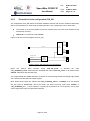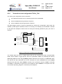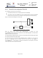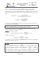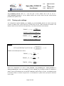
1
SpaceWire CODEC IP
User Manual
Ref:
Uod_Link_User
Document Revision:
2.4
Date:
27th March 2009
SpaceWire Interface User.doc
Ref.:
SpaceWire CODEC IP
User Manual
UoD-Link-User
2.4
Issue: 27 March 2009
Date: Page: 2 / 69
Document Ref: UoD_Link_User
Issue No:
2.4
Issue Date:
27th March 2009
Author:
Chris McClements
VHDL Code:
tag “uodcodec_cvsrel_2_3”
Number of pages in document:
69
Document History:
Date
Issue
Description
Ref
6-Oct-2003
draft
New UoD CODEC VHDL user manual
cmc
19-Apr-2004
1.1
DDR output multiplexer synthesis description updated
cmc
27-Oct-05
1.2
Use Latches configuration removed
cmc
CFG_SLOWRATE_SYSCLK description updated
2-July-2007
2.1
Fixed serial reset problem of txencode and transmit clock
generators.
cmc
-
2.2
Not released
cmc
22 January
2008
2.3
Update with CFG_SLOWCLK_10MHZ reference signal
cmc
27 Mar 2009
2.4
Corrections after ESTEC review
cmc
Page 2 of 69
Ref.:
SpaceWire CODEC IP
User Manual
I
UoD-Link-User
2.4
Issue: 27 March 2009
Date: Page: 3 / 69
CONTENTS
I
CONTENTS ..................................................................................................................................... 3
II
LIST OF FIGURES .......................................................................................................................... 6
III
LIST OF TABLES ............................................................................................................................ 8
1
SCOPE ............................................................................................................................................ 9
2
APPLICABLE DOCUMENTS ........................................................................................................ 10
3
DEFINITIONS ................................................................................................................................ 11
4
3.1
TERMS AND DEFINITIONS ........................................................................................................... 11
3.2
VHDL CODE TERMS AND DEFINITIONS....................................................................................... 11
3.3
DOCUMENT TERMS AND DEFINITIONS ......................................................................................... 12
CONFIGURATION MANAGEMENT ............................................................................................. 13
4.1
5
6
DIRECTORY STRUCTURE ........................................................................................................... 13
4.1.1
CODEC RTL files ............................................................................................................ 14
4.1.2
VHDL File Hierachy ......................................................................................................... 15
FUNCTIONAL OVERVIEW ........................................................................................................... 16
5.1
SYSTEM OVERVIEW................................................................................................................... 16
5.2
FUNCTIONS............................................................................................................................... 16
5.2.1
Configuration Overview ................................................................................................... 17
5.2.2
Initialisation State Machine .............................................................................................. 17
5.2.3
Receiver .......................................................................................................................... 17
5.2.4
Receiver Credit Counter .................................................................................................. 18
5.2.5
Receiver Error Recovery ................................................................................................. 18
5.2.6
Transmitter ...................................................................................................................... 18
5.2.7
Transmitter Clock Generator ........................................................................................... 18
5.2.8
Transmitter Credit Counter .............................................................................................. 18
5.2.9
Transmitter Error Recovery ............................................................................................. 18
TOP LEVEL CLOCK AND CONFIGURATION INTERFACE ....................................................... 20
6.1
CFG_RXBUF_ADDRLEN ....................................................................................................... 20
6.2
CFG_RATE_NUMBITS .......................................................................................................... 20
6.3
SYSTEM RESET......................................................................................................................... 20
6.4
SYSTEM CLOCK ......................................................................................................................... 21
6.5
TRANSMIT BIT CLOCK................................................................................................................. 21
6.5.1
Transmit clock configuration SYS_DEFAULT ................................................................. 23
Page 3 of 69
Ref.:
SpaceWire CODEC IP
User Manual
7
UoD-Link-User
2.4
Issue: 27 March 2009
Date: Page: 4 / 69
6.5.2
Transmit clock configuration SYS_SLOWCLK ................................................................ 24
6.5.3
Transmit bit clock configuration SYS_SLOWCLK_DIV ................................................... 25
6.5.4
Transmit bit clock configuration SYS_DIV ...................................................................... 26
6.5.5
Transmit bit clock configuration SYS_EN ....................................................................... 27
6.5.6
Transmit bit clock configuration TXCLK_DEFAULT ........................................................ 28
6.5.7
Transmit bit clock configuration TXCLK_SLOWCLK ...................................................... 29
6.5.8
Transmit bit clock configuration TXCLK_SLOWCLK_DIV .............................................. 30
6.5.9
Transmit bit clock configuration TXCLK_ DIV ................................................................. 31
6.5.10
Transmit bit clock configuration TXCLK_EN ................................................................... 32
6.5.11
Variable data rate and default 10Mbits/sec data rate generation ................................... 33
6.5.12
Double Data Rate outputs ............................................................................................... 34
6.5.13
Transmit clock configuration and signals overview ......................................................... 35
6.6
10/5 MHZ REFERENCE CLOCK (SLOWCLK) ............................................................................. 36
6.7
RECEIVE BUFFER CLOCK............................................................................................................ 36
6.8
PIPELINING ............................................................................................................................... 36
6.9
DISCARDING EMPTY PACKETS ................................................................................................... 37
6.10
MAXIMUM OUTSTANDING CREDIT ............................................................................................ 37
6.11
TRANSMIT TIME-CODE HANDLING ........................................................................................... 37
6.12
INTENAL RECEIVER DISCONNECT AND INIT FSM TIMEOUT COUNTERS ....................................... 38
6.13
TIMING CYCLE SETTINGS ........................................................................................................ 39
6.14
DISCONNECT TIMEOUT UNCERTAINTY .................................................................................... 40
6.15
CONFIGURATION SIGNALS OVERVIEW ..................................................................................... 40
INTERNAL INTERFACE ............................................................................................................... 42
7.1
LINK STATE OPERATION ............................................................................................................ 42
7.1.1
Link Start-up .................................................................................................................... 42
7.1.2
Link Disable ..................................................................................................................... 43
7.2
DATA INTERFACE ...................................................................................................................... 43
7.2.1
Transmit........................................................................................................................... 43
7.2.2
Transmit FIFO signals operation. .................................................................................... 43
7.2.3
Receive ............................................................................................................................ 44
7.2.4
Receive buffer signals operation ..................................................................................... 44
7.2.5
Data Received ................................................................................................................. 44
7.2.6
Host read ......................................................................................................................... 44
7.2.7
Flags ................................................................................................................................ 45
7.2.8
Receive buffer clock frequency. ...................................................................................... 45
7.2.9
Maximum input bit rate dependent on receive buffer clock frequency ............................ 47
7.2.10
Data Interface Signals ..................................................................................................... 48
7.3
TIMECODE INTERFACE ............................................................................................................... 48
7.3.1
Transmit........................................................................................................................... 49
Page 4 of 69
Ref.:
SpaceWire CODEC IP
User Manual
UoD-Link-User
2.4
Issue: 27 March 2009
Date: Page: 5 / 69
7.3.2
Receive ............................................................................................................................ 49
7.3.3
Timecode Interface Signals ............................................................................................. 49
7.4
STATUS SIGNALS ...................................................................................................................... 50
7.5
ERROR RECOVERY ................................................................................................................... 51
8
7.5.1
Transmitter Error Recovery ............................................................................................. 51
7.5.2
Transmitter Buffer Flushing ............................................................................................. 51
7.5.3
Receiver Error Recovery ................................................................................................. 51
EXTERNAL INTERFACE .............................................................................................................. 53
8.1
9
DATA STROBE ENCODING.......................................................................................................... 53
8.1.1
Single data rate outputs .................................................................................................. 53
8.1.2
Double data rate outputs ................................................................................................. 53
8.1.3
Data Strobe Timing ......................................................................................................... 55
8.1.4
Serial Interface signals .................................................................................................... 56
SYNTHESIS ................................................................................................................................... 57
9.1
GENERAL.................................................................................................................................. 57
9.2
MEMORY .................................................................................................................................. 57
9.3
VENDOR SPECIFIC INFORMATION ............................................................................................... 57
9.3.1
10
XST .................................................................................................................................. 57
STATIC TIMING ANALYSIS ..................................................................................................... 59
10.1
CLOCK CONSTRAINT ANALYSIS ............................................................................................... 59
10.2
RECEIVER CLOCK STATIC TIMING ANALYSIS ........................................................................... 60
10.2.1
Timing Parameters .......................................................................................................... 60
10.2.2
Data Setup Check ........................................................................................................... 61
10.2.3
Strobe Setup Check ........................................................................................................ 62
10.2.4
Minimum Pulse Width ...................................................................................................... 63
10.2.5
Skew Tolerance ............................................................................................................... 64
10.3
GENERIC TRANSMITTER DOUBLE DATA RATE OUTPUTS .......................................................... 65
10.3.1
Generic DDR output method one .................................................................................... 65
10.3.2
Generic DDR Method Two .............................................................................................. 67
11
CONFORMITY ........................................................................................................................... 68
12
APPENDIX I – CLOCK MULTIPLEXER .................................................................................... 69
Page 5 of 69
Ref.:
SpaceWire CODEC IP
User Manual
II
UoD-Link-User
2.4
Issue: 27 March 2009
Date: Page: 6 / 69
LIST OF FIGURES
Figure 4-1 CODEC directory structure .................................................................................................. 13
Figure 4-2 VHDL files hierarchy ............................................................................................................ 15
Figure 5-1 User Implementation with UoD Codec ................................................................................ 16
Figure 6-1 SYS_DEFAULT transmit clock configuration ...................................................................... 23
Figure 6-2 SYS_SLOWCLK transmit clock configuration ..................................................................... 24
Figure 6-3 SYS_SLOWCLK_DIV transmit clock configuration ............................................................. 25
Figure 6-4 SYS_DIV transmit clock configuration ................................................................................. 26
Figure 6-5 SYS_EN transmit clock configuration .................................................................................. 27
Figure 6-6 TX_DEFAULT transmit clock configuration ......................................................................... 28
Figure 6-7 TX_SLOWCLK transmit clock configuration ........................................................................ 29
Figure 6-8 TX_SLOWCLK_DIV transmit clock configuration ................................................................ 30
Figure 6-9 TXCLK_DIV transmit clock configuration ............................................................................ 31
Figure 6-10 TXCLK_EN transmit clock configuration ........................................................................... 32
Figure 6-11 Receive buffer data flow .................................................................................................... 36
Figure 6-12 CFG_SLOW_CE_SEL configuration signals ..................................................................... 38
Figure 6-13 Additional time added when loading state machine counter ............................................. 40
Figure 6-14 Disconnect timeout uncertainty (100ns period) ................................................................. 40
Figure 7-1 Initialisation state machine .................................................................................................. 42
Figure 7-2 Transmit Timing Specification ............................................................................................. 44
Figure 7-3 Receive timing specification ................................................................................................ 45
Figure 7-4 Minimum Receive buffer clock frequency ............................................................................ 46
Figure 7-5 TICK_IN interface ................................................................................................................ 49
Figure 7-6 TICK_OUT interface ............................................................................................................ 49
Figure 8-1 Generic DOUT and SOUT DDR encode ............................................................................. 53
Figure 8-2 Transmit DDR register “transmit/txddrreg.vhd” ................................................................... 54
Figure 8-3 txddrreg_noenable.vhd double data rate generation logic and waveform .......................... 54
Figure 8-4 Vendor specific DOUT and SOUT DDR encode ................................................................. 55
Figure 9-1 ISE coregent settings for rxnchar_resync_ff.vhd ................................................................. 58
Figure 10-1 Receive Clock Data Recovery ........................................................................................... 60
Figure 10-2 Data Setup Time Timing Diagram ..................................................................................... 62
Figure 10-3 Large clock delay setup time violation ............................................................................... 62
Figure 10-4 Latest Strobe Setup Time When no Skew ........................................................................ 63
Figure 10-5 Data and Strobe Skew effects on Strobe Setup Time ....................................................... 63
Page 6 of 69
Ref.:
SpaceWire CODEC IP
User Manual
UoD-Link-User
2.4
Issue: 27 March 2009
Date: Page: 7 / 69
Figure 10-6 Minimum Pulse Width ........................................................................................................ 64
Figure 10-7 Data Skew Tolerance ........................................................................................................ 64
Figure 10-8 Maximum Strobe Skew ...................................................................................................... 65
Figure 10-9 DDR output encoding (Method one) .................................................................................. 65
Figure 10-10 DDR output multiplexer select ......................................................................................... 66
Figure 10-11 DDR output multiplexer timing specification .................................................................... 66
Figure 10-12 Method Two DDR output encoding ................................................................................. 67
Figure 12-1 Glitch Free clock multiplexer ............................................................................................. 69
Page 7 of 69
Ref.:
SpaceWire CODEC IP
User Manual
III
UoD-Link-User
2.4
Issue: 27 March 2009
Date: Page: 8 / 69
LIST OF TABLES
Table 2-1 Applicable Documents .......................................................................................................... 10
Table 4-1 Directory descriptions ........................................................................................................... 14
Table 4-2 RTL file descriptions ............................................................................................................. 15
Table 6-1 Output Reset Values ............................................................................................................. 21
Table 6-2 CFG_BITCLK options ........................................................................................................... 22
Table 6-3 Transmit configuration and signals overview ........................................................................ 35
Table 6-4 Configuration signals overview ............................................................................................. 41
Table 7-1 Link control signals ............................................................................................................... 43
Table 7-2 Transmit data interface signals ............................................................................................. 48
Table 7-3 Receive data interface signals .............................................................................................. 48
Table 7-4 Timecode interface signals ................................................................................................... 50
Table 7-5 Status signals ........................................................................................................................ 51
Table 7-6 Error Recovery Signals ......................................................................................................... 52
Table 8-1 Serial interface signals .......................................................................................................... 56
Table 10-1 Status timing clock analysis ................................................................................................ 59
Table 10-2 Data and Clock Recovery Timing Parameters ................................................................... 61
Table 10-3 Extra Clock Recovery Timing Parameters .......................................................................... 61
Table 10-4 Skew Tolerance Maximums................................................................................................ 64
Page 8 of 69
Ref.:
SpaceWire CODEC IP
User Manual
1
UoD-Link-User
2.4
Issue: 27 March 2009
Date: Page: 9 / 69
SCOPE
This document defines how the University of Dundee SpaceWire CODEC VHDL code shall be used.
Page 9 of 69
Ref.:
SpaceWire CODEC IP
User Manual
2
UoD-Link-User
2.4
Issue: 27 March 2009
Date: Page: 10 / 69
APPLICABLE DOCUMENTS
In this section the documents referenced in this document are listed.
Document Reference
ECSS-E-ST-50-12C
(31July2008)
Ref
[AD1]
Document name
European Cooperation for Space Standardization,
SpaceWire – Links, Nodes, Routers and Networks
March 2003..
Table 2-1 Applicable Documents
Page 10 of 69
Ref.:
SpaceWire CODEC IP
User Manual
3
UoD-Link-User
2.4
Issue: 27 March 2009
Date: Page: 11 / 69
DEFINITIONS
In this Document the following conventions are used.
3.1
Terms and definitions
Bit rate
Number of bits transmitted/received every second
byte
Eight bits of information
DDR
Double data rate. Two bits of data transmitted for each transmit clock period.
FCT
Flow control token. Transmitter sends one FCT when room in receive buffer for eight
more N-chars.
Init FSM
SpaceWire exchange level initialisation state machine which controls start-up and link
connection.
Jitter
N-char
The time uncertainty of a low to high or high to low edge measured with respect to
other edges in that signal.
Data character, EOP or EEP.
Null
Character transmitted by SpaceWire link to keep connection with other end.
SDR
Single data rate. One bit of data transmitted for each transmit clock period.
Skew
The timing difference between two signals due to differences in the signal path length.
UoD
University of Dundee
ECSS
European cooperation for space standardization
3.2
VHDL Code Terms and Definitions
In the VHDL code the following VHDL conventions are:
VHDL entity architecture pairs are placed in the same VHDL file. The filename is a lowercase
equivalent of the entity name, e.g. The entity rxcredit is represented in the file “rxcredit.vhd”.
All VHDL entity names can be mixed case or lower case.
All VHDL signal and port names are in UPPERCASE. Signals which have multi word names are split
with an underscore character, e.g. credit error is represented as CREDIT_ERROR.
For all signals the “ieee.std_logic_1164” STD_LOGIC and STD_LOGIC_VECTOR types are used. This
ensures that all types are consistent through all VHDL files and no conversions between STD_LOGIC
and STD_ULOGIC are required or necessary.
For all vector signals the highest number index is the MSB and the lowest number index is the LSB.
i.e. the (n downto 0) vector type is used
For all arithmetic signals the “ieee.numeric_std” UNSIGNED type is used. Arithmetic functions such as
+, - or = are implemented in the numeric_std package.
Page 11 of 69
Ref.:
SpaceWire CODEC IP
User Manual
UoD-Link-User
2.4
Issue: 27 March 2009
Date: Page: 12 / 69
Conversions from UNSIGNED to STD_LOGIC_VECTOR are implemented using type conversion e.g.
STD_LOGIC_VECTOR(unsigned_signal). Conversions from STD_LOGIC_VECTOR to UNSIGNED
are implemented using type conversion e.g. UNSIGNED(std_logic_vector_signal).
Conversions from UNSIGNED
to integer are implemented using the numeric_std function
to_integer(unsigned_sig). Conversions from integers to UNSIGNED are implemented using the
numeric_std function to_unsigned(integer_val, sign_length).
Active low signals are labelled SIGNAL_NAME_N.
Output signals from entities are often required internally for circuit feedback purposes. Redundant
signals which are required for this purpose are labelled PORT_SIGNAL_i and assigned to the output
in the code as PORT_SIGNAL <= PORT_SIGNAL_i in the VHDL code.
3.3
Document Terms and Definitions
In this Document the following conventions are used.
Signal and port names are written using the bold “courier new” font. e.g. SIGNAL_NAME.
Page 12 of 69
Ref.:
SpaceWire CODEC IP
User Manual
4
UoD-Link-User
2.4
Issue: 27 March 2009
Date: Page: 13 / 69
CONFIGURATION MANAGEMENT
4.1
Directory Structure
The directory structure of the SpaceWire CODEC directory structure is shown in the list below.
Figure 4-1 CODEC directory structure
A description of each directory is listed in the Table 4-1.
Directory
Function
docs
Location of documentation files
src/vhdl
Location of RTL VHDL files
src/vhdl/initfsm
Initialisation state machine VHDL files
src/vhdl/other
Generic and miscellaneous VHDL files
src/vhdl/receive
Data strobe decoder and receive credit counter VHDL files
src/vhdl/transmit
Data strobe encoder VHDL files
src/vhdl/txclk
Transmit clock generation VHDL files
src/vhdl/top
SpaceWire CODEC top level VHDL files
src/verif
Location of verification files, scripts and test case commands
src/verif/cmd
Command files which perform the verification test cases of the SpaceWire
CODEC
src/verif/scripts
Scripts to compile and run the verification of the SpaceWire CODEC.
src/verif/gen-tb
General testbench components and units VHDL files
src/verif/package
Testbench VHDL package files
src/verif/spwr-tb
Control, status, data and time-code interface control for the testbench VHDL
SpaceWire link
src/verif/uut-tb
Control, status, data and time-code interface control for the UUT SpaceWire link
src/verif/top
Top level testbench components.
verif/rtl
RTL verification directory where the verification run is performed. (reference
directory for scripts)
Page 13 of 69
Ref.:
SpaceWire CODEC IP
User Manual
UoD-Link-User
2.4
Issue: 27 March 2009
Date: Page: 14 / 69
Table 4-1 Directory descriptions
4.1.1
CODEC RTL files
The RTL files are found in the “codec_actel/ip/codec_actel/src/vhdl” directory.
File
Description
Initialisation state machine
initfsm/init_fsm.vhd
Initialisation state machine
initfsm/initfsm_counter.vhd
Initialisation state machine counter
initfsm/initfsm_sync.vhd
Synchronisation of receiver signals for
initialisation state machine
Generic files
other/clk10gen.vhd
Generation of 100 ns clock enable pulse
other/clkmux.vhd
Clock multiplexer for multiplexing two clocks
with an asynchronous signal
Receive Files
receive/rxclock.vhd
Receiver clock recovery exclusive or gate
receive/rxcredit.vhd
Receiver credit counter and receive buffer
pointer management
receive/rxdecode.vhd
receive bit-stream decoder. Decodes the
input bit-stream input SpaceWire character
receive/rxdataformat.vhd
Receive data formatter. Formats double
EOPs into a form which can be synchronised
between receive clock and receive buffer
successfully.
receive/rxnchar_resync_ff.vhd
Receive data resynchronisation to receive
buffer clock
receive/rxnchar_resync_ffstore.vhd
Receive data resynchronisation data storage
flip-flops
receive/rxnchar_resync_ffstore_inferfpgaram.vhd
Receive data resynchronisation data storage
written to infer FPGA ram.
receive/rxnchar_resync_ffcell.vhd
Memory row built from flip-flops.
receive/rxnchar_resync_and.vhd
And gate for memory output multiplexer
receive/rxnchar_resync_dataena.vhd
Data enabled for memory output multiplexer
receive/rxnchar_resync_demux.vhd
De-multiplexer for writing to memory
receive/rxnchar_resync_valid.vhd
Presents valid data synchronised with the
empty flag
receive/rxdiscerr.vhd
Receiver disconnect detection
receive/rxtcode_resync.vhd
Receiver time-code resynchronisation from
receive clock to system clock
Transmit files
transmit/txencode.vhd
Serial output bit-stream encoder
transmit/txtcode_send.vhd
Time-code input component
transmit/txddrreg.vhd
Transmit double data rate register
Page 14 of 69
Ref.:
SpaceWire CODEC IP
User Manual
transmit/txddrreg_noenable.vhd
UoD-Link-User
2.4
Issue: 27 March 2009
Date: Page: 15 / 69
Transmit double data rate register without
clock enable generated data rate.
Variable data rate files
txclk/txclkgen.vhd
Transmit clock generation and multiplexing
component
txclk/txclk_divider.vhd
Transmit clock divider to generate different
data rates
txclk/txclk_en_gen.vhd
Generation of variable rate transmit data rate
enable pulse
Table 4-2 RTL file descriptions
4.1.2
VHDL File Hierachy
The hierarchy of the VHDL files is described in the following tree diagram.
top/spwrlink.vhd
|
\--+ others/clk10gen.vhd
|
\--+ initfsm/init_fsm.vhd
| \--+ initfsm/initfsm_counter.vhd
| \--+ initfsm/initfsm_resync.vhd
|
\--+ receive/rxcredit.vhd
\--+ receive/rxdecode.vhd
\--+ receive/rxtcode_resync.vhd
\--+ receive/rxnchar_resync_ff.vhd
| \--+ receive/rxnchar_resync_demux.vhd
| \--+ receive/rxnchar_resync_dataena.vhd
| \--+ receive/rxnchar_resync_valid.vhd
|
\--+ transmit/txencode.vhd
\--+ transmit/txtcode_send.vhd
|
\--+ txclk/txclkgen.vhd
| \--+ txclk/txclk_en_gen.vhd
| \--+ txclk/txclk_divider.vhd
|
\--+ others/clkmux.vhd
Figure 4-2 VHDL files hierarchy
Page 15 of 69
Ref.:
SpaceWire CODEC IP
User Manual
5
UoD-Link-User
2.4
Issue: 27 March 2009
Date: Page: 16 / 69
FUNCTIONAL OVERVIEW
In this section an overview of the SpaceWire Codec architecture is provided.
5.1
System Overview
A block diagram of the SpaceWire CODEC and expected usage is given in Figure 5-1.
Figure 5-1 User Implementation with UoD Codec
5.2
Functions
The UoD CODEC is a high speed serial transmitter/receiver compliant with the SpaceWire standard
[AD1]. The SpaceWire CODEC is responsible for making a connection with the SpaceWire interface
Page 16 of 69
Ref.:
SpaceWire CODEC IP
User Manual
UoD-Link-User
2.4
Issue: 27 March 2009
Date: Page: 17 / 69
at the other end of a link and managing the flow of N-char across the link. The interface transmits and
receives SpaceWire characters which can be link characters (L-Char) or normal characters (N-char).
L-Chars are characters that are used to manage the flow of N-char across a link (NULL & FCT). Nchars are the characters that are used to pass information across the link (N-char characters, EOP,
EEP and TIMECODEs).
The following sub-sections define the functional blocks which make up the SpaceWire interface are
listed below.
5.2.1
Configuration Overview
The UoD SpaceWire codec can be configured to suit the users application as follows:
Pipelined to increase transmission speed or non pipelined to save area.
DDR outputs or SDR outputs depending the on required data rate and the users selected
technology.
Transmission clock configuration options to allow an independent transmit clock and default
reference clock therefore greatly increasing the achievable data rate and decoupling the
transmit logic from the system clock logic.
Internal variable data rate generation.
Configurable receive buffer size. Internal FCT credit counter operations are handled
internally.
5.2.2
Initialisation State Machine
The CODEC state machine is responsible for initiating a connection on the link and performing related
synchronisation.
The state machine determines its next state by monitoring receiver signals which indicate the type of
characters received and any receiver errors. The state machine enables the transmitter to send
NULLs, FCTs, N-char characters, time-codes and end of packet markers (EOP and EEP).
5.2.3
Receiver
The receiver is responsible for decoding the received data-strobe encoded bit-stream into SpaceWire
characters. The receiver reports the type of characters received and any errors encountered to the
initialisation state machine which enables and disables the receiver as appropriate. The receiver is
implemented in two parts, a decoder which decodes characters in the receiver clock domain and a
synchroniser, which then synchronises receiver signals to the system clock domain. This method
ensures all receiver outputs are synchronous to the system clock.
Page 17 of 69
Ref.:
SpaceWire CODEC IP
User Manual
5.2.4
UoD-Link-User
2.4
Issue: 27 March 2009
Date: Page: 18 / 69
Receiver Credit Counter
The receiver credit counter keeps a record of the buffer space available in the receiver FIFO and the
number of characters which have been requested from the link. This allows the CODEC to implement
flow control.
The receiver credit counter implements the receiver buffer pointers. This makes the implementation of
the receiver credit counter and the receiver buffer more efficient as the number of counters required is
kept to a minimum.
5.2.5
Receiver Error Recovery
The receiver error recovery block recovers the receiver credit counters and the receiver FIFO after an
error occurs. After an error an EEP marker is added to the receiver FIFO. The receiver credit counter
must be updated because all previously transmitted FCTs are discarded at the other end of the link
due to error recovery.
5.2.6
Transmitter
The transmitter is responsible for transmitting L-Chars and N-chars over a link using data-strobe
encoding. The interface state machine determines which type of character the transmitter can send
over the link. The transmitter accepts N-char characters and end of packet markers from the
transmitter FIFO. N-char characters are transmitted when there is data in the FIFO and the transmitter
has credit to send one more N-char. The transmitter sends an FCT character for each block of space
for eight N-chars in the receive FIFO. As the host system reads out data from the receive FIFO so the
transmitter sends more FCTs to indicate that the receiver has room to receive eight more N-chars.
The transmitter sends NULLs when there is no other information to send.
5.2.7
Transmitter Clock Generator
The transmitter clock enable generator is responsible for generating the variable transmitter bit-rate
and default data signalling rate depending on the configuration.
5.2.8
Transmitter Credit Counter
The transmitter credit counter holds a count register which indicates the number of SpaceWire N-char
characters which can be sent along the link.
5.2.9
Transmitter Error Recovery
The transmitter error recovery module recovers the transmitter FIFO after an error occurs. In a
network situation the first byte of a packet is interpreted as the packet address, therefore the error
recovery block reads from the transmitter FIFO until the next end of packet marker was read from the
Page 18 of 69
Ref.:
SpaceWire CODEC IP
User Manual
UoD-Link-User
2.4
Issue: 27 March 2009
Date: Page: 19 / 69
FIFO. The transmitter is allowed to start up when error recovery is taking place but the transmitter is
prevented from reading from the transmit FIFO until error recovery is complete
Page 19 of 69
Ref.:
SpaceWire CODEC IP
User Manual
6
UoD-Link-User
2.4
Issue: 27 March 2009
Date: Page: 20 / 69
TOP LEVEL CLOCK AND CONFIGURATION INTERFACE
The following sections define the internal and external interfaces which are employed in the UoD
SpaceWire CODEC. Each section has a detailed description of the signal functions and an overview
table for each signal and the clock which the signal is synchronous to.
Note: The configuration constants mentioned in the following sections are defined in the package
“top/spwrlink_pkg.vhd”.
6.1
CFG_RXBUF_ADDRLEN
The configuration constant CFG_RXBUF_ADDRLEN determines the length of the read and write
addresses for the receive buffer and therefore the size of the receive buffer. The buffer size is defined
as:
2^
rxbufaddrlen
.
For example, the receive buffer address length is 10, the receive buffer size will be 1 Kbytes. The
SpaceWire CODEC will automatically handle FCT credit operations dependent on the size of the
buffer.
6.2
CFG_RATE_NUMBITS
The configuration constant CFG_RATE_NUMBITS determines the signal length of slow rate and
transmitter rate inputs. The signal length determines the size of the internal down counters used for
variable data rate generation. The signals CFG_SLOWRATE_TXCLK, CFG_SLOWRATE_SYSCLK and
TXRATE are affected by the generic ratenumbits.
6.3
System Reset
The interface signal RST_N is an active low asynchronous reset of the UoD CODEC. The RST_N
signal should be asserted for at least two system clock cycles to ensure synchronous reset elements
register the reset.
The transmitter is reset synchronously to ensure no simultaneous transitions occur of DOUT/SOUT.
The reset values are listed in Table 6-1.
Signal
Reset Value
Comments
DOUT
„0‟
Reset in controlled manner
DOUT_F
„0‟
Reset in controlled manner
SOUT
„0‟
Reset in controlled manner
DOUT_F
„0‟
Reset in controlled manner
Page 20 of 69
Ref.:
SpaceWire CODEC IP
User Manual
UoD-Link-User
2.4
Issue: 27 March 2009
Date: Page: 21 / 69
XENR
„0‟
Reset in controlled manner
XENF
„0‟
Reset in controlled manner
DOUT_CLR_N
„0‟
Reset in controlled manner
SOUT_CLR_N
„0‟
Reset in a controlled manner
TICK_OUT
„0‟
TIME_OUT
All „0‟
RXBUF_DATA
Undefined
RXBUF_WRADDR
All „0‟
RXBUF_RDADDR
All „0‟
RXBUF_WRVALID
„0‟
RXBUF_RDVALID
„0‟
RXBUF_EMPTY
„1‟
RXBUF_PROGFLAG
„0‟
TX_FIFO_READ
„0‟
DISC_RUN_ERROR
„0‟
PARITY_RUN_ERROR
„0‟
ESCAPE_RUN_ERROR
„0‟
CREDIT_RUN_ERROR
„0‟
STATUS(15:0)
All „0‟
Data storage is not reset. Data is valid
on RXBUF_WRVALID
Table 6-1 Output Reset Values
6.4
System clock
The interface signal SYSCLK clocks the interface state machine which controls link start-up and link
reconnection after an error is detected. The system clock can also clock the receiver buffer and the
transmitter dependent on the configuration signals.
6.5
Transmit bit clock
The UoD SpaceWire CODEC can be configured to implement a number of transmission clocking
schemes.. The valid transmitter bit clock configurations can be selected by the user via the package
constant CFG_BITCLK. The valid configurations are listed in Table 6-2
The transmit bit clock configuration determines the source or method used for the following:
Baseline bit clock (system clock or independent transmit clock).
10MHz default data signalling rate (internally generated or input SLOWCLK)
Variable data signalling rate (not enabled, clock enables or clock divider)
Page 21 of 69
Ref.:
SpaceWire CODEC IP
User Manual
CFG_BITCLK
Symbolic name(1)
UoD-Link-User
2.4
Issue: 27 March 2009
Date: Page: 22 / 69
Input clock
Default 10/5MHz(2)
Variable data rate
SYSCLK
SYSCLK
“0000” (0h)
SYS_DEFAULT
SYSCLK
“0001”(1h)
SYS_SLOWCLK
SYSCLK
SLOWCLK
SYSCLK
“0010”(2h)
SYS_SLOWCLK_DIV
SYSCLK
SLOWCLK
Clock divider
“0011” (3h)
SYS_DIV
SYSCLK
Clock divider
Clock divider
“0100” (4h)
SYS_EN
SYSCLK
“1000” (8h)
TXCLK_DEFAULT
TXCLK
Clock enable
TXCLK
Clock enable
TXCLK
“1001” (9h)
TXCLK_SLOWCLK
TXCLK
SLOWCLK
TXCLK
“1010” (Ah)
TXCLK_SLOWCLK_DIV
TXCLK
SLOWCLK
Clock divider
“1011” (Bh)
TXCLK_DIV
TXCLK
Clock divider
Clock divider
“1100”(Ch)
TXCLK_EN
TXCLK
Clock enable
Clock enable
Table 6-2 CFG_BITCLK options
Note 1: The symbolic names are defined as VHDL constants in the package “top/spwrlink_pkg.vhd”.
Note 2: 10MHz for single data rate or 5MHz for double data rate.
The following sub sections define the meaning of the configurations in Table 6-2.
Note: The following configurations reference the use a glitch free multiplexer to select between two
asynchronous clocks. . Appendix I, in section 12, details the design of the glitch free multiplexer.
Page 22 of 69
Ref.:
SpaceWire CODEC IP
User Manual
6.5.1
UoD-Link-User
2.4
Issue: 27 March 2009
Date: Page: 23 / 69
Transmit clock configuration SYS_DEFAULT
The SYS_DEFAULT configuration is used when SYSCLK is equal to the default 10MHz data
signalling rate. The SYSCLK frequency should be set to 10MHz when single data rate is used or
5MHz when DDR outputs are used.
Note: The data rate in this configuration is fixed to 10Mbits/s as the SYSCLK input is used as the
timings reference (state machine timeout and receive disconnect timeout).
This configuration is the most efficient implementation of the UoD SpaceWire CODEC, as:
No internal clock generation is required.
Synchronisation of signals is not required between SYSCLK and the transmit bit clock.
SYSCLK is used as the 10/5Mhz reference clock for disconnect detection and state machine
timeouts.
Figure 6-1 shows the transmission scheme configuration
DOUT
DOUT_F
SYSCLK
Tx
Encode
SOUT
SOUT_F
XENR
XENF
Figure 6-1 SYS_DEFAULT transmit clock configuration
Page 23 of 69
Ref.:
SpaceWire CODEC IP
User Manual
6.5.2
UoD-Link-User
2.4
Issue: 27 March 2009
Date: Page: 24 / 69
Transmit clock configuration SYS_SLOWCLK
The SYS_SLOWCLK configuration can be used when an independent 10MHz clock is used for the
default 10Mbits/sec transmit rate and the transmitter clock is the system clock. No internal variable
data rate generator is implemented. The SLOWCLK frequency should be set to 10MHz when single
data rate is used or 5MHz when DDR outputs are used.
This configuration can be implemented when:
Only one system clock is used and no internal variable data rate generation is required. The
system clock frequency can be changed externally if required..
An external 10/5MHz reference clock is desired.
Figure 6-2 shows the clock configuration SYS_SLOWCLK.
FSM.SEL_SLOW
SYSCLK
DOUT
0
DOUT_F
TXBITCLK
Tx
Encode
SOUT
SLOWCLK
1
SOUT_F
(Glitch Free Clock Multiplexer)
XENR
XENF
Figure 6-2 SYS_SLOWCLK transmit clock configuration
Page 24 of 69
Ref.:
SpaceWire CODEC IP
User Manual
6.5.3
UoD-Link-User
2.4
Issue: 27 March 2009
Date: Page: 25 / 69
Transmit bit clock configuration SYS_SLOWCLK_DIV
The transmit clock configuration SYS_SLOWCLK_DIV allows an independent 10/5MHz default
transmit rate (SLOWCLK) and a generated variable transmit rate from SYSCLK. This configuration
generates a new transmit clock tree asynchronous from SYSCLK. The SYS_SLOWCLK_DIV
configuration can be used when.
An internal variable data rate scheme is required and the transmit clock is SYSCLK.
An external 10/5MHz reference clock is desired.
The configuration SYS_DIV is shown in Figure 6-4.
XIMAX
=0
FSM.SEL_SLOW
TXRATE
Prog
Divider
XI_DIV_CLK
0
DOUT
XCLK_DIV
SYSCLK
DOUT_F
0
TXBITCLK
1
Tx
Encode
SOUT
(Glitch Free Clock Multiplexer)
SLOWCLK
SOUT_F
1
(Glitch Free Clock Multiplexer)
XENR
XENF
Figure 6-3 SYS_SLOWCLK_DIV transmit clock configuration
The variable data rate is implemented using a programmable divider which enables a toggle flip-flop.
When the SpaceWire CODEC is performing link start-up (FSM.SEL_SLOW) the input SLOWCLK is
selected. When link start-up has been performed and a link connection has been established the input
TXRATE determines the data rate. When TXRATE is equal to zero (maximum rate) then XIMAX is
asserted and SYSCLK is selected by the glitch free clock multiplexer. When TXRATE is not equal to
zero the clock generator output XI_CLK_DIV is selected by the multiplexer.
Synchronisation is automatically performed by the SpaceWire CODEC as TXBITCLK
asynchronous to SYSCLK in this configuration.
Page 25 of 69
is
Ref.:
SpaceWire CODEC IP
User Manual
6.5.4
UoD-Link-User
2.4
Issue: 27 March 2009
Date: Page: 26 / 69
Transmit bit clock configuration SYS_DIV
The transmit clock configuration SYS_DIV allows a variable rate and default 10MHz transmitter bit
clock to be generated from SYSCLK. This configuration generates a new transmit clock tree
asynchronous from SYSCLK. The SYS_ DIV configuration can be used when:
A variable data rate scheme is required but the use of clock enables is not desired (typically
clock enabled DDR outputs not supported when external vendor specific DDR outputs are
used).
An external 10MHz reference clock is not available.
The configuration SYS_DIV is shown in Figure 6-4.
=0
XIMAX
FSM.SEL_SLOW
DOUT
TXRATE
CFG_SLOWRATE_TXCLK
Prog
Divider
XI_DIV_CLK
0
DOUT_F
TXBITCLK
Tx
Encode
SOUT
SYSCLK
1
SOUT_F
(Glitch Free Clock Multiplexer)
XENR
XENF
Figure 6-4 SYS_DIV transmit clock configuration
The variable data rate and 10MHz default data rate are implemented using a programmable divider
which enables a toggle flip-flop. When the SpaceWire CODEC is performing link start-up
(FSM.SEL_SLOW) the input CFG_SLOWRATE_TXCLK determines the frequency of TXBITCLK. When
link start-up has been performed and a link connection has been established the input TXRATE
determines the data rate. When TXRATE is equal to zero (maximum rate) then XIMAX is asserted
and SYSCLK is selected by the glitch free clock multiplexer. When TXRATE is not equal to zero the
clock generator output XI_CLK_DIV is selected by the multiplexer.
Synchronisation is automatically performed by the SpaceWire CODEC as TXBITCLK
asynchronous to SYSCLK in this configuration.
Page 26 of 69
is
Ref.:
SpaceWire CODEC IP
User Manual
6.5.5
UoD-Link-User
2.4
Issue: 27 March 2009
Date: Page: 27 / 69
Transmit bit clock configuration SYS_EN
The configuration SYS_EN allows the default 10Mbits/s transmit rate and the variable transmission
rate to be generated by an internal clock enable generator. This configuration can be used when:
The number of clock nets available to the user is limited (only one clock net is required for this
transmission scheme).
TXBITCLK is synchronous with SYSCLK.
Figure 6-5 shows the block diagram for SYS_EN.
DOUT
DOUT_F
SYSCLK
Tx
Encode
SOUT
SOUT_F
FSM.SEL_SLOW
TXRATE
CFG_SLOWRATE_TXCLK
XENR
Clock
Enable
Generator
XENF
Figure 6-5 SYS_EN transmit clock configuration
When
the
internal
state
machine
signal
FSM.SEL_SLOW
is
asserted
the
input
CFG_SLOWRATE_TXCLK determines the final data-rate. When FSM.SEL_SLOW is de-asserted then
TXRATE determines the final data-rate.
The outputs XENR and XENF should be connected to the rising edge enable and falling edge enable
of the transmit double data rate output register.
Note: When DDR outputs are selected and CFG_SLOWRATE_TXCLK or TXRATE is an odd number
the duty cycle on DOUT/SOUT will not be 50/50. The worst case duty cycle, when TXRATE or
CFG_SLOWRATE_TX = 1, will be 75/25 (i.e. 15ns/5ns for 2 transitions at a 20 ns period). This is still a
valid configuration under the SpaceWire standard.
Page 27 of 69
Ref.:
SpaceWire CODEC IP
User Manual
6.5.6
UoD-Link-User
2.4
Issue: 27 March 2009
Date: Page: 28 / 69
Transmit bit clock configuration TXCLK_DEFAULT
The TXCLK_DEFAULT can be used when:
An independent transmit clock is required (asynchronous to SYSCLK)
All transmit clock generation is implemented externally, e.g. external PLL.
The SpaceWire standard states a default 10Mbits/s transmit rate shall be used at start-up. To
implement this requirement the user can monitor the link running status bit and determine the TXCLK
input frequency. i.e. when the link is not running (not in run state) the TXCLK frequency should be
10/5 MHz. When the link is running then TXCLK can be set to any frequency up to the maximum
frequency supported by the users implementation.
LINK_RUNING
External
Clock
generation
(e.g. PLL)
DOUT
DOUT_F
TXCLK
Tx
Encode
SOUT
SOUT_F
XENR
XENF
Figure 6-6 TX_DEFAULT transmit clock configuration
Page 28 of 69
Ref.:
SpaceWire CODEC IP
User Manual
6.5.7
UoD-Link-User
2.4
Issue: 27 March 2009
Date: Page: 29 / 69
Transmit bit clock configuration TXCLK_SLOWCLK
The TXCLK_SLOWCLK configuration can be used when:
An independent transmit clock is required (asynchronous to SYSCLK)
Transmit clock variable data rate is implemented externally or fixed.
An independent 10/5MHz reference clock is desired.
The block diagram shown in Figure 6-7 describes the TX_SLOWCLK configuration. When the
FSM.SEL_SLOW signal is asserted, the link is not running or is starting up, then SLOWCLK is
selected by the glitch free multiplexer. When the link is running then TXCLK is selected as the
transmit bit clock.
FSM.SEL_SLOW
TXCLK
DOUT
0
DOUT_F
TXBITCLK
Tx
Encode
SOUT
SLOWCLK
1
SOUT_F
(Glitch Free Clock Multiplexer)
XENR
XENF
Figure 6-7 TX_SLOWCLK transmit clock configuration
Page 29 of 69
Ref.:
SpaceWire CODEC IP
User Manual
6.5.8
UoD-Link-User
2.4
Issue: 27 March 2009
Date: Page: 30 / 69
Transmit bit clock configuration TXCLK_SLOWCLK_DIV
The TXCLK_SLOWCLK_DIV configuration can be used when:
An independent transmit clock is required (asynchronous to SYSCLK)
Internal variable data rate generation is required.
An independent 10/5MHz reference clock is required and available externally.
The variable data rate is implemented using a programmable divider which enables a toggle flip-flop.
When the SpaceWire CODEC is performing link start-up (FSM.SEL_SLOW) the input TXCLK is
selected. When link start-up has been performed and a link connection has been established the input
TXRATE determines the data rate. When TXRATE is equal to zero (maximum rate) then XIMAX is
asserted and TXCLK is selected by the glitch free clock multiplexer. When TXRATE is not equal to
zero the clock generator output XI_CLK_DIV is selected by the multiplexer.
XIMAX
=0
FSM.SEL_SLOW
TXRATE
Prog
Divider
XI_DIV_CLK
0
DOUT
XCLK_DIV
TXCLK
DOUT_F
0
TXBITCLK
1
Tx
Encode
SOUT
(Glitch Free Clock Multiplexer)
SLOWCLK
SOUT_F
1
(Glitch Free Clock Multiplexer)
XENR
XENF
Figure 6-8 TX_SLOWCLK_DIV transmit clock configuration
Page 30 of 69
Ref.:
SpaceWire CODEC IP
User Manual
6.5.9
UoD-Link-User
2.4
Issue: 27 March 2009
Date: Page: 31 / 69
Transmit bit clock configuration TXCLK_ DIV
The TXCLK_DIV configuration can be used when:
An independent transmit clock is required (asynchronous to SYSCLK)
Internal variable data rate generation is required.
Internal 10Mbits/s data rate generation is required..
The block diagram shown in Figure 6-8 describes the TXCLK_DIV configuration. When either the
FSM.SEL_SLOW signal is asserted, the link is not running or it is starting up, then TXCLK is selected
by the glitch free multiplexer. When the link is running the internally generated XI_DIV_CLK clock is
selected.
=0
XIMAX
FSM.SEL_SLOW
DOUT
TXRATE
CFG_SLOWRATE_TXCLK
Prog
Divider
XI_DIV_CLK
0
DOUT_F
TXBITCLK
Tx
Encode
SOUT
TXCLK
1
SOUT_F
(Glitch Free Clock Multiplexer)
XENR
XENF
Figure 6-9 TXCLK_DIV transmit clock configuration
The variable data rate and the 10MHz default data rate are implemented using a programmable
divider which enables a toggle flip-flop. When the SpaceWire CODEC is performing link start-up
(FSM.SEL_SLOW) the input CFG_SLOWRATE_TXCLK determines the frequency of TXBITCLK. When
link start-up has been performed and a link connection has been established the input TXRATE
determines the data rate. When TXRATE is equal to zero (maximum rate) then XIMAX is asserted
and TXCLK is selected by the glitch free clock multiplexer. When TXRATE is not equal to zero the
clock divider output XI_CLK_DIV is selected by the multiplexer.
Page 31 of 69
Ref.:
SpaceWire CODEC IP
User Manual
6.5.10
UoD-Link-User
2.4
Issue: 27 March 2009
Date: Page: 32 / 69
Transmit bit clock configuration TXCLK_EN
The configuration TXCLK_EN can be used when:
An independent transmit clock is required (asynchronous to SYSCLK)
The number of clock nets available to the user is limited (TXCLK is used as the baseline
transmit clock and synchronous clock enables are used to generate the variable data rate)
Figure 6-10 shows the block diagram for TXCLK_EN.
DOUT
DOUT_F
TXCLK
Tx
Encode
SOUT
SOUT_F
FSM.SEL_SLOW
TXRATE
CFG_SLOWRATE_TXCLK
XENR
Clock
Enable
Generator
XENF
Figure 6-10 TXCLK_EN transmit clock configuration
When
the
internal
state
machine
signal
FSM.SEL_SLOW
is
asserted
the
input
CFG_SLOWRATE_TXCLK determines the final data-rate. When FSM.SEL_SLOW is de-asserted then
TXRATE determines the final data-rate.
The outputs XENR and XENF should be connected to the rising edge enable and falling edge enable
of the transmit double data rate output register.
Note: When DDR output are selected and CFG_SLOWRATE_TXCLK or TXRATE is an odd number the
duty cycle on DOUT/SOUT will not be 50/50. The worst case duty cycle, when TXRATE or
CFG_SLOWRATE_TX = 1, will be 75/25 (i.e. 15ns/5ns for 2 transitions at a 20 ns period). This is still a
valid configuration under the SpaceWire standard.
Page 32 of 69
Ref.:
SpaceWire CODEC IP
User Manual
6.5.11
UoD-Link-User
2.4
Issue: 27 March 2009
Date: Page: 33 / 69
Variable data rate and default 10Mbits/sec data rate generation
In the previous sections the signals CFG_SLOWRATE_TXCLK and TXRATE are used to determine the
variable and default data rates. The following functions should be used to determine the value of each
signal.
The top level generic CFG_RATENUMBITS should be set according to the maximum value which will
be used to divide the value TxMaxBitRate.
Warning: TXRATE is used in the transmit clock domain therefore should be synchronous to the
SpaceWire link signal TXBITCLK. In some configurations TXBITCLK is variable.
The following examples show values of CFG_SLOWRATE_TXCLK and TXCLK dependent on the
maximum bit rate and also the generic ratenumbits.
Example 1 - TxMaxBitRate = 200Mbits/s
If TXRATE is equal to 3 then:
If the slowest clock speed is 10Mbits/sec (CFG_SLOWRATE_TXCLK=19) the generic ratenumbits
should be set to 5 (2^5 max value = 31)
Example 2 - TxMaxBitRate = 66Mbits/s
Note: both values above are inside the 10Mbits/s +/- 10% defined in the SpaceWire standard.
Page 33 of 69
Ref.:
SpaceWire CODEC IP
User Manual
6.5.12
UoD-Link-User
2.4
Issue: 27 March 2009
Date: Page: 34 / 69
Double Data Rate outputs
The configuration input CFG_DDROUT determines if the transmit encoder outputs will be encoded as
double data rate (DDR) or single data rate. Two bits per clock cycle are output for each bit clock
period when CFG_DDROUT is equal to „1‟.
The UoD SpaceWire CODEC does not implement an internal DDR output register, but one is provided
for reference in the file “transmit/txddrreg.vhd”. This allows the user to implement a vendor specific
DDR output register scheme, e.g. Virtex2 DDR output buffers, if appropriate. The usage of DDR
output buffers is described in section 8.1.2.
Page 34 of 69
UoD-Link-User
Ref.:
SpaceWire CODEC IP
User Manual
6.5.13
2.4
Issue: 27 March 2009
Date: Page: 35 / 69
Transmit clock configuration and signals overview
signal/constant
Type
Description
Sync To Clk
TXCLK
In
Independent transmit clock
n/a
SLOWCLK
In
Independent 10/5 MHz reference
clock.
n/a
CFG_BITCLK(3:0)
In
Configuration selection for
transmit clock
n/a
CFG_SLOWRATE_TXCLK
In
Divider value to derive the
10Mbits/s default rate when
generated internally.
TXCLK when CFG_BITCLK =
TXCLK_*, SYSCLK when
CFG_BITCLK = SYS_*
TXRATE
In
Divider value to derive the
variable transmit rate, when it is
generated internally.
TXCLK when CFG_BITCLK =
TXCLK_*, SYSCLK when
CFG_BITCLK = SYS_*
XENR
Out
Clock enable for rising edges
when CFG_BITCLK =
SYS/TXCLK_EN
TXBITCLK
XENF
Out
Clock enable for falling edges
when CFG_BITCLK =
SYS/TXCLK_EN
TXBITCLK
Table 6-3 Transmit configuration and signals overview
Page 35 of 69
Ref.:
SpaceWire CODEC IP
User Manual
6.6
UoD-Link-User
2.4
Issue: 27 March 2009
Date: Page: 36 / 69
10/5 MHz Reference Clock (SLOWCLK)
The interface signal SLOWCLK can be used to input a 10/5 MHz reference clock for the UoD
SpaceWire CODEC. Depending on the transmit clock configuration, SLOWCLK can provide the default
10Mbits/s data signalling rate at start-up and connection.
SLOWCLK is also used as the reference clock for receive disconnect detection and state machine
timeout detection. This is the most efficient implementation as no internal counter is required to
generate a 10MHz reference clock enable signal, although extra synchronisation is required between
the system clock domain and the 10MHz clock domain.
When a double data rate configuration is used the bit rate is twice the SLOWCLK clock speed, i.e.
5MHz clock and double data rate output gives 10Mbit/s. For better resolution of the disconnect and
state machine timers a 10MHz reference clock rate can be used by setting CFG_SLOWCLK_10MHZ to
„1‟. Internally the 10MHz signal is divided to give a 5MHz reference clock to the transmitter when
initialisation is performed.
6.7
Receive buffer clock.
The user can select which clock is used to resynchronise N-chars from the receiver clock domain and
write them to the receiver buffer. When the configuration signal CFG_SYNCRDCLK = „1‟ then SYSCLK
is used. When CFG_SYNCRDCLK = „0‟ the input RDCLK is used.
The interface signal RDCLK can be used as an independent read clock for the receiver buffer. This
can be useful if very high data rates are implemented and RDCLK should be partitioned from SYSCLK.
The receive buffer data flow is shown in Figure 6-11
DIN
SIN
4 Byte Re-sync
Buffer
Receiver
Receive Clock
Domain
Receive buffer
Clock Domain
Receive Buffer
CODEC boundary
Figure 6-11 Receive buffer data flow
6.8
Pipelining
The configuration signal CFG_PIPELINE allows the UoD SpaceWire CODEC to insert pipeline
registers where appropriate to decrease the delays between flip-flops and increase clock speed and
transmission speed.
When CFG_PIPELINE = „1‟ then an extra cycle of latency is required to transmit/receive one
Timecode/N-char
Page 36 of 69
Ref.:
SpaceWire CODEC IP
User Manual
UoD-Link-User
2.4
Issue: 27 March 2009
Date: Page: 37 / 69
An increase in area footprint can be expected when CFG_PIPELINE is equal to „1‟.
6.9
Discarding Empty Packets
The configuration input signal CFG_DISCARD_EMPTY_PACKET when equal to „1‟ discards packets
which have no cargo and consist only of an EOP/EEP.
6.10
Maximum Outstanding credit
The configuration input signal CFG_MAXCREDIT
should be set to the maximum number of
outstanding N-chars which can be expected by the UoD SpaceWire CODEC. The maximum number
of N-chars should be set in accordance with the generic rxbufaddrlen.
For example if a 16 byte buffer is used then CFG_MAXCREDIT could be set to any value between 8
and 16. If CFG_MAXCREDIT is set to greater than 16 the UoD SpaceWire link CODEC will not request
more than 16 outstanding characters. Typically the user should set CFG_MAXCREDIT to the
maximum value their buffer will support up to the value 56.
The binary equivalent of the maximum outstanding credit value should be placed on
CFG_MAXCREDIT(5:0). i.e. Maximum outstanding N-chars is 32 then CFG_MAXCREDIT should be
set to “100000”.
For SpaceWire compliant operation the following condition must be met:
8 <= CFG_MAXCREDIT <= 56.
Note the CFG_MAXCREDIT value does not have to be a factor of 8 and can be equal to 9,10 etc.
6.11
Transmit Time-code Handling
The configuration constant CFG_TICK_IN_KEEP determines how the SpaceWire interface handles
TICK_IN requests when the link is not running.
The default behaviour of the link (CFG_TICK_IN_KEEP=0) discards time-codes when the interface is
not in the run state. When the link is running time-codes are transmitted with priority over other
characters as normal.
The legacy behaviour of the link (CFG_TICK_IN_KEEP=1) keeps time-codes in a 1 time-code storage
buffer until the link enters the run state. If a new time-code is requested to be transmitted (TICK_IN)
the currently held time-code is discarded and the new time-code is the next time-code to be sent.
When the link enters the run state the held time-code will be immediately sent.
Page 37 of 69
Ref.:
SpaceWire CODEC IP
User Manual
6.12
UoD-Link-User
2.4
Issue: 27 March 2009
Date: Page: 38 / 69
Intenal receiver disconnect and Init FSM timeout Counters
If the CFG_BITCLK configuration signal is set to a value which does not support an external 10/5MHz
clock signal the internal receiver disconnect and state machine timeout counters will be enabled from
an internal or external 10MHz clock
enable pulse generator.
The configuration signal
CFG_SLOW_CE_SEL determines if an internal or external clock enable pulse is used. If an internal
clock
enable
generator
CFG_SLOWRATE_SYSCLK.
is
used
the
number
of
clock
cycles
Additional to CFG_SLOWRATE_SYSCLK
to
count
is
set
to
the configuration signals
TIMING_6_4, TIMING_12_8 and TIMING_850ns determine the number of cycles of the clock
enable pulse to count.
The diagram below shows the configuration steps between the configuration signals and the internal
SpaceWire link blocks.
Figure 6-12 CFG_SLOW_CE_SEL configuration signals
When the signal CFG_SLOW_CE_SEL = „1‟ the input SLOW_CE will be selected as the 10MHz clock
enable pulse. When CFG_SLOW_CE_SEL = „0‟ then an internal 10MHz pulse will be generated
dependent on the signal CFG_SLOWRATE_SYSCLK. The CFG_SLOWRATE_SYSCLK value should be
set via the function equation
Equation 6-1 CFG_SLOWRATE_SYSCLK (rounded down to nearest integer)
Example System Clock Frequency = 30MHz
The system clock frequency may not provide an adequate 10MHz timeout rate for the initialisation
state machine timeouts, i.e. a system clock is 25MHz gives a clock period of 40 ns and a
Page 38 of 69
Ref.:
SpaceWire CODEC IP
User Manual
UoD-Link-User
2.4
Issue: 27 March 2009
Date: Page: 39 / 69
CFG_SLOWRATE_SYSCLK value of 1. This will give a clock enable rate of 80 ns, 40 ns *
(CFG_SLOWRATE_SYSCLK+1), for the 10MHz timeout rate counter which will give invalid timeout
periods for the system clock.
6.13
Timing cycle settings
The configuration signals TIMING_6_4, TIMING_12_8 and TIMING_850ns are used to select the
number of 10MHz clock cycles which are counted for the 6.4us, 12.8us and 850 ns timeouts. The
default values are set to 64 and 128 respectively. The values should be set as follows
TIMING _ 6 _ 4
6.4 s
SlowClockRate
Equation 6-2 Deriving TIMING_6_4
TIMING _ 12 _ 8
12.8 s
SlowClockRate
Equation 6-3 Deriving TIMING_12_8
Example System Clock Frequency = 25MHz (40 ns period)
10 MHz clock enable period is =80 ns
TIMING _ 6 _ 4
6.4 s
80ns
TIMING _ 12 _ 8
12.8 s
80ns
160
850ns
80ns
11
TIMING _ 850ns
80
When the configuration bit clock is SYS_SLOWCLK, SYS_SLOWCLK_DIV, TXCLK_SLOWCLK or
TXCLK_SLOWCLK_DIV then the TIMING_6_4 and TIMING_12_8 settings should be adjusted to
allow for the synchronisation time to load the initialisation state machine counter. The additional time
to load the counter, as shown in Figure 6-13, is calculated as 1 system clock cycle plus 3 reference
clock cycles.
Page 39 of 69
Ref.:
SpaceWire CODEC IP
User Manual
UoD-Link-User
2.4
Issue: 27 March 2009
Date: Page: 40 / 69
Figure 6-13 Additional time added when loading state machine counter
Example System Clock Frequency = 30MHz (33.333 ns period), CFG_BITCLK=SYS_SLOWCLK.
6.14
Disconnect Timeout Uncertainty
The disconnect period of the SpaceWire link is specified to be from 727ns to 1000ns, see the
SpaceWire Standard section 8.11.12. In the SpaceWire CODEC model the timeout period for the
disconnect timeout counter has a one cycle uncertainty. For example, if the disconnect timer is set to
9 cycles of a 100ns period timeout clock the disconnect period will be from 800 ns to 900 ns as shown
in Figure 6-14.
Figure 6-14 Disconnect timeout uncertainty (100ns period)
6.15
Configuration Signals Overview
Signal
Type
Description
Sync To
Clk
CFG_SYNCRDCLK
In
Is receive buffer clock synchronous to SYSCLK
n/a
CFG_PIPELINE
In
Should pipelining flip-flops be inserted into the
UoD SpaceWire CODEC to increase achievable
data rate.
n/a
Page 40 of 69
Ref.:
SpaceWire CODEC IP
User Manual
UoD-Link-User
2.4
Issue: 27 March 2009
Date: Page: 41 / 69
CFG_DISCARD_EMPTY_PKT
In
Should empty packets be discarded by the
receiver
n/a
CFG_MAXCREDIT
In
RXBUF_CLK
CFG_SLOWRATE_SYSCLK
In
Maximum outstanding credit the receive buffer
credit counter can hold.
Number of clock cycles for a 10MHz rate.
TIMING_6_4
In
Number of 10MHz rate clock cycles to count for
the 6.4µs timeout.
n/a
TIMING_12_8
In
Number of 10MHz rate clock cycles to count for
the 12.8µs timeout.
n/a
TIMING_850ns
In
Number of 10MHz rate clock cycles to count for
the 850 ns disconnect period timer.
n/a
Table 6-4 Configuration signals overview
Page 41 of 69
n/a
UoD-Link-User
Ref.:
2.4
Issue: 27 March 2009
Date: Page: 42 / 69
SpaceWire CODEC IP
User Manual
7
INTERNAL INTERFACE
The following sub-sections define the operation of the UoD SpaceWire CODEC..
7.1
Link State Operation
The link state operation signals control the enabling and disabling of the SpaceWire CODEC. The
SpaceWire link state machine is shown in Figure 7-1.
Reset
RxErr OR
CreditError OR
[Link Disabled]
ErrorReset
Reset Tx
Reset Rx
RxErr OR
gotFCT OR
gotN-Char OR
gotTime-Code
After 6.4 µs
Run
Send Time-Codes/
FCTs/N-Chars/NULLs
Enable Rx
RxErr OR
gotFCT OR
gotN-Char OR
gotTime-Code
gotFCT
RxErr OR
gotN-Char OR
gotTime-Code OR
after 12.8 µs
Connecting
Send FCTs/NULLs
Enable Rx
gotNULL
RxErr OR
gotFCT OR
gotN-Char OR
gotTime-Code OR
after 12.8 µs
Started
Send NULLs
Enable Rx
ErrorWait
Reset Tx
Enable Rx
After
12.8 µs
Ready
Reset Tx
Enable Rx
[Link Enabled]
Figure 7-1 Initialisation state machine
7.1.1
Link Start-up
Link start-up is implemented as described in [AD1] (section 8.5). The CODEC attempts to make a
connection with the other end of the link when in state Started. The interface state machine moves to
Started when in state Ready and LINK_ENABLED is asserted. The signal LINK_ENABLED is defined
below.
LINK_ENABLED = (not LINK_DISABLED) and (LINK_START or (AUTO_START and
GOT_NULL))
When LINK_START is asserted and LINK_DISABLED is de-asserted the CODEC will always try to
establish a connection with the other end of the link. If no connection is established, i.e. no NULLs
received, after sending NULLs for 12.8 us the exchange of silence protocol is performed. If a NULL is
received then an FCT character is expected before moving to the Run state where data and
timecodes can be transmitted.
Page 42 of 69
Ref.:
SpaceWire CODEC IP
User Manual
UoD-Link-User
2.4
Issue: 27 March 2009
Date: Page: 43 / 69
When AUTO_START is asserted and LINK_START and LINK_DISABLE are de-asserted the
CODEC will remain in state Ready until reception of a NULL.
7.1.2
Link Disable
Link Disable is implemented as described in [AD1] section 8.5. LINK_DISABLE should be asserted
to cause a safe link disconnection. Error recovery is performed when LINK_DISABLE causes the
state machine to move from Run to ErrorReset.
Link start-up signals are listed in Table 7-1.
Signal
Type
Description
Sync To
Clk
LINK_START
In
Enable the CODEC to establish a connection.
SYSCLK
LINK_DISABLE
In
Disable or stop the CODEC. When LINK_DISABLE is asserted
it causes the initialisation state machine to move from Run to
ErrorReset then error recovery is performed.
SYSCLK
AUTOSTART
In
Auto start the CODEC. When set the CODEC will wait in state
Ready until the first NULL character is received.
SYSCLK
Table 7-1 Link control signals
7.2
Data Interface
The data interface consists of a transmit interface and a receive interface. As shown in Figure 5-1 a
transmitter FIFO and receiver buffer should be placed between the UoD SpaceWire CODEC and the
host data bus controller, or equivalent.
The transmit FIFO should be reset when the CODEC is reset.
7.2.1
Transmit
The transmit FIFO should be clocked by the UoD SpaceWire CODEC signal TXBITCLK. This ensures
that the maximum data rate can be achieved by allowing the transmitter to read data characters
synchronously from the transmit FIFO using the transmit clock. In cases where TXBITCLK can be
variable the transmit FIFO should be capable of independent read and write clock operation.
7.2.2
Transmit FIFO signals operation.
When the host FIFO has data then it should de-assert the CODEC input signal TX_FIFO_EMPTY and
place the data on the input TX_FIFO_DATA(8:0). The transmitter asserts TX_FIFO_READ for one
cycle to read the data into the transmitter for transmission over the link. The interface between the
transmitter FIFO and the transmitter bus controller, or equivalent, is dependent on the application. The
expected transmitter FIFO interface waveforms are shown in Figure 7-2.
Page 43 of 69
UoD-Link-User
Ref.:
SpaceWire CODEC IP
User Manual
1
2
3
4
5
6
7
8
9
2.4
Issue: 27 March 2009
Date: Page: 44 / 69
10
11
12
TXBITCLK
TX_FIFO_EMPTY
TX_FIFO_DATA
DATA
EOP
DATA
TX_FIFO_READ
Figure 7-2 Transmit Timing Specification
Note:- If a read from the FIFO causes the FIFO to become empty on the next clock cycle the empty
signal must be asserted before the next clock cycle. (e.g. cycle 4 above)
Note:- After an EOP transmit (4 serial bits) the next data character can be read immediately for
transmission
7.2.3
Receive
The receive port of the UoD SpaceWire CODEC implements the read, write and FCT pointers for the
receive buffer. The user simply has to choose the size of the read buffer and implement the memory
storage for received N-chars.
7.2.4
Receive buffer signals operation
All receive buffer output signals as synchronous to RXBUF_CLK.
Note: The receiver buffer pointers are implemented synchronously to RXBUF_CLK as N-chars are
resynchronised to the RXBUF_CLK domain before being written to the receiver buffer. This allows
EEPs to be written to the receive buffer when an error occurs
7.2.5
Data Received
On reception of a data character the data is placed on the output signal RXBUF_DATA(8:0) and
RXBUF_WRVALID
is asserted for one cycle (see figures Figure 5-1 and Figure 7-3) .
RXBUF_WRVALID should be connected to the write enable port of the receive buffer. If a credit error
occurs, N-char(s) received when not expected/requested, the link is disconnected and the error bytes
are written to the receive buffer if not full. If the receive buffer is full the N-chars are discarded. The
output RXBUF_WRADDR should be connected to the write address port of the memory storage used
for the receive buffer.
7.2.6
Host read
When the user reads an N-char from the receive buffer the signal RXBUF_READ should be asserted
for one RXBUF_CLK cycle. The UoD CODEC will assert the signal RXBUF_RDVALID if the read is
Page 44 of 69
UoD-Link-User
Ref.:
SpaceWire CODEC IP
User Manual
2.4
Issue: 27 March 2009
Date: Page: 45 / 69
valid, i.e. the FIFO is not empty. The output RXBUF_RDVALID can be connected to the enable port of
the receive buffer storage output register if required. The output RXBUF_RDADDR should be
connected to the read address port of the storage method used for the receive buffer.
7.2.7
Flags
The receive port implements an empty flag, RXBUF_EMPTY, and a programmable flag,
RXBUF_PROGFLAG, for the receive buffer. The empty flag is asserted when there are no N-chars in
the buffer. The programmable flag is asserted when the number of characters in the buffer equals the
input signal RXBUF_PROGVAL. In this way a half full or almost full flag can be generated dependent on
the user application needs.
Note: The RXBUF_PROGFLAG has a one clock cycle latency before assertion and de-assertion
therefore it should be used as a guide for half full and almost full
Figure 7-3 shows the timing specification for the receive buffer signals.
1
2
3
4
5
6
7
8
9
10
11
12
RXBUF_CLK
RXBUF_WRADDR
0
1
2
RXBUF_WRVALID
RXBUF_DATA
RXBUF_RDADDR
XX
AA
XX
0
1
BB
XX
2
RXBUF_READ
RXBUF_RDVALID
RXBUF_EMPTY
Figure 7-3 Receive timing specification
Note: RXBUF_READ can be asserted when the receive buffer is empty. The read pointer will only be
updated when RXBUF_RDVALID is asserted (The FIFO is not empty).
7.2.8
Receive buffer clock frequency.
The minimum frequency of the receive buffer clock is dependent on the maximum data rate the
SpaceWire CODEC will receive and the minimum size of packets which will be expected by the
SpaceWire CODEC.
Page 45 of 69
Ref.:
SpaceWire CODEC IP
User Manual
UoD-Link-User
2.4
Issue: 27 March 2009
Date: Page: 46 / 69
Minimum read clock with different input bit rates
BitRate
Tdata
Teop
MinNumData
1.E+9
10.E-9
4.E-09
1
500.E+6
20.E-9
8.E-09
1
200.E+6
50.E-9 20.E-09
1
100.E+6
100.E-9 40.E-09
1
50.E+6
200.E-9 80.E-09
1
25.E+6
400.E-9 160.E-09
1
Tpacket Taverage MinRdClk
14.E-09
7.E-09
142.857E+06
28.E-09
14.E-09
71.429E+06
70.E-09
35.E-09
28.571E+06
140.E-09
70.E-09
14.286E+06
280.E-09 140.E-09
7.143E+06
560.E-09 280.E-09
3.571E+06
Minimum read clock with different minimum packet data sizes
BitRate
Tdata
Teop
MinNumData
200.E+6
50.E-9 20.E-09
0
200.E+6
50.E-9 20.E-09
1
200.E+6
50.E-9 20.E-09
2
200.E+6
50.E-9 20.E-09
3
200.E+6
50.E-9 20.E-09
4
200.E+6
50.E-9 20.E-09
5
200.E+6
50.E-9 20.E-09
6
200.E+6
50.E-9 20.E-09
7
200.E+6
50.E-9 20.E-09
8
200.E+6
50.E-9 20.E-09
9
200.E+6
50.E-9 20.E-09
10
Tpacket Taverage MinRdClk
20.E-09
20.E-09
50.E+06
70.E-09
35.E-09
28.571E+06
120.E-09
40.E-09
25.E+06
170.E-09
43.E-09
23.529E+06
220.E-09
44.E-09
22.727E+06
270.E-09
45.E-09
22.222E+06
320.E-09
46.E-09
21.875E+06
370.E-09
46.E-09
21.622E+06
420.E-09
47.E-09
21.429E+06
470.E-09
47.E-09
21.277E+06
520.E-09
47.E-09
21.154E+06
Legend
MinNumData=0
EOP
MinNumData=1
DATA
EOP
MinNumData=2
DATA
DATA
EOP
MinNumData=3
DATA
DATA
DATA
EOP
etc..
Tdata
Time for one data byte to be received
Teop
Time for one EOP byte to be received
Tpacket
Time for one packet to be received
Taverage
Average time for one N-Char to be received
MinRdClk
Minimum frequency of read clock to resynchronise n-chars
Figure 7-4 Minimum Receive buffer clock frequency
From the table above the function for minimum read clock frequency is:
Page 46 of 69
Ref.:
SpaceWire CODEC IP
User Manual
UoD-Link-User
2.4
Issue: 27 March 2009
Date: Page: 47 / 69
and MinNumData is the minimum number of data bytes in a packet.
The table and functions above shows the absolute minimum frequency for RXBUF_CLK. Dependent
on the actual bit-rate (transmit clock +/- values) or the average jitter on DIN/SIN a tolerance should
be added to the receive buffer clock e.g. +1%.
Example: If characters are received at the maximum rate then jitter on DIN and SIN and therefore
RXCLK can cause the Taverage time to drop below the expected value. For example if jitter on
DIN/SIN caused the bit rate to vary between 200 and 205 Mbits/sec then Taverage will vary between
34 and 35 ns therefore the minimum read clock should be 29.286 MHz.
7.2.9
Maximum input bit rate dependent on receive buffer clock frequency
Analysis of the maximum input bit-rate can be useful when the receive buffer clock frequency is fixed.
E.g. receive buffer clock is tied to the system clock which is dependent on an external processor.
The function below shows the maximum input bit-rate dependent on the receive buffer clock:
Example: If the receive buffer frequency is 50MHz and the minimum packet expected is 1 Nchar+ EOP then
Trxbuf_clk = 20ns, and NumPktNchars = 2, and NumPktBits = 14,
therefore
i.e. The maximum bit rate can be 7 times the receive buffer clock rate when MinNumData = 1
Page 47 of 69
Ref.:
SpaceWire CODEC IP
User Manual
7.2.10
UoD-Link-User
2.4
Issue: 27 March 2009
Date: Page: 48 / 69
Data Interface Signals
Data interface signals are listed in Table 7-3
Signal
Type
Description
Sync To
Clk
TX_FIFO_DATA
In
Transmitter data which is read by the transmitter. The most
significant bit is the data control flag which indicates if the
character is an end of packet or data character.
TXBITCLK
TX_FIFO_READ
Out
Asserted when the transmitter reads one N-char from the
transmitter FIFO.
TXBITCLK
TX_FIFO_EMPTY
In
Transmitter FIFO empty flag indicates the empty status of
the transmitter. When high the transmitter is empty.
TXBITCLK
Table 7-2 Transmit data interface signals
Note TXBITCLK may be = SYSCLK, SLOWCLK or divided clock.
Signal
Type
Description
Sync To
Clk
RXBUF_DATA
Out
Receiver data which is written from the receiver to the
receiver FIFO. The most significant bit is the character
control flag which indicates when the character is an end
of packet marker.
RXBUF_CLK
RXBUF_WRVALID
Out
Asserted when data is received and ready on
RXBUF_DATA.
RXBUF_CLK
RXBUF_WRADDR
Out
Address to write RXBUF_DATA to.
RXBUF_CLK
RXBUF_EMPTY
Out
Empty flag for receive buffer. When asserted then no data
is in the buffer
RXBUF_CLK
RXBUF_READ
In
Read from receive buffer. Asserted for one RXBUF_CLK
period
RXBUF_CLK
RXBUF_RDVALID
Out
Asserted when RXBUF_READ is asserted and the buffer is
not empty.
RXBUF_CLK
RXBUF_RDADDR
Out
Address to read data from the receive buffer. Updated on
a valid read
RXBUF_CLK
RXBUF_PROGFLAG
Out
Programmable flag which can be used to indicate a halffull condition or as a level indicator
RXBUF_CLK
RXBUF_PROGVAL
Out
Programmable flag value
RXBUF_CLK
Table 7-3 Receive data interface signals
7.3
Timecode Interface
The timecode interface consists of a transmit and receive interface. Timecode signals are
synchronous to the system clock.
Page 48 of 69
Ref.:
2.4
Issue: 27 March 2009
Date: Page: 49 / 69
SpaceWire CODEC IP
User Manual
7.3.1
UoD-Link-User
Transmit
The host timecode controller will typically include a six bit counter which is incremented/decremented
when a timecode is transmitted. The timecode value should be placed on the input TIME_IN(7:0)
and TICK_IN should be asserted when a timecode is to be transmitted. TICK_IN can be asserted
for more than one clock cycle but only one timecode will be transmitted. The timecode value which is
present on TIME_IN on the rising edge of SYSCLK when TICK_IN is asserted will be transmitted.
The timecode timing specification is shown in Figure 7-5.
1
2
3
4
5
6
7
8
9
10
11
12
SYSCLK
TICK_IN
TIME_IN
T1
Figure 7-5 TICK_IN interface
Note:- No timecode buffering is employed and if the CODEC is not in state Run the TICK_IN request
is ignored. This is consistent with the nature of timecode processing in a SpaceWire network.
7.3.2
Receive
On reception of a timecode the signal TICK_OUT is asserted and the timecode value is placed on the
output TIME_OUT(7:0). The TIME_OUT value is registered in the RXCLK clock domain and is valid
only on the rising edge SYSCLK when TICK_OUT is asserted. The TIME_OUT interface is shown in
Figure 7-6.
1
2
3
4
5
6
7
8
9
10
11
SYSCLK
TICK_OUT
TIME_OUT
T1
Figure 7-6 TICK_OUT interface
7.3.3
Timecode Interface Signals
Timecode interface signals are listed in
Signal
TIME_IN(7:0)
Type
In
Description
Sync
To Clk
Timestamp which is sent over the SpaceWire link when the
SYSCLK
Page 49 of 69
12
Ref.:
SpaceWire CODEC IP
User Manual
UoD-Link-User
2.4
Issue: 27 March 2009
Date: Page: 50 / 69
control signal TICK_IN is asserted. The timecode is sent
immediately after the transmitter has completed sending
the previous character.
TICK_IN
In
Tick-in strobe causes a timecode to be sent over the
spacewire link. The signal is synchronous.
SYSCLK
TIME_OUT(7:0)
Out
Received timecode output. The timecode on TIME_OUT is
valid when TICK_OUT is asserted.
RXCLK
TICK_OUT
Out
Asserted when a timecode is received and the timecode
on TIME_OUT is valid. The TICK_OUT signal is
synchronous to the system clock.
SYSCLK
Table 7-4 Timecode interface signals
7.4
Status Signals
Status reporting is performed through the output signal STATUS(15:0). Run errors are reported
through the *_RUNERR output signals
The status bits are listed in Table 7-5
Signal
Type
Description
Sync to
Clk
DISC_RUN_ERR
Out
Disconnect error in run state
SYSCLK
PARITY_RUN_ERR
Out
Parity error in run state
SYSCLK
ESCAPE_RUN_ERR
Out
Escape error in run state
SYSCLK
CREDIT_RUN_ERR
Out
Transmit or receive credit error in run state
SYSCLK
STATUS(15:0)
Out
SpaceWire interface status signals. All status signals are
synchronous to CLK
SYSCLK
STATUS(0)
Out
Disconnect error.
SYSCLK
STATUS(1)
Out
Parity error.
SYSCLK
STATUS(2)
Out
Escape error.
SYSCLK
STATUS(3)
Out
Receiver credit error. The receiver has received more data
characters then requested
SYSCLK
STATUS(4)
Out
SYSCLK
STATUS(7:5)
Out
STATUS(8)
Out
Transmitter credit error. The transmitter has credit to send
more than the allowed 56 data characters.
Interface state encoded into three bits (6 states)
Interface state machine is in the Run state.
STATUS(9)
Out
Receiver got NULL. Remains asserted after first NULL.
SYSCLK
STATUS(10)
Out
Receiver got FCT. Remains asserted after first FCT
SYSCLK
STATUS(11)
Out
Receiver got N-chars. Remains asserted after first N-Char
SYSCLK
STATUS(12)
Out
SYSCLK
STATUS(13)
Out
Receiver got Timecodes. Remains asserted after first
Timecode
Transmitter has credit to send one more data character
STATUS(14)
Out
N-char sequence error (N-char received before link state is
Run)
SYSCLK
STATUS(15)
Out
Timecode sequence error (Timecode received before link
SYSCLK
Page 50 of 69
SYSCLK
SYSCLK
SYSCLK
Ref.:
SpaceWire CODEC IP
User Manual
UoD-Link-User
2.4
Issue: 27 March 2009
Date: Page: 51 / 69
state is Run)
Table 7-5 Status signals
The state encoding used for STATUS(7:5) is shown in the following table
STATUS(7:5)
Interface state
ErrorReset
“000”
ErrorWait
“001”
Ready
“010”
Started
“011”
Connecting
“100”
Run
“101
7.5
Error Recovery
Error recovery is initiated when the CODEC state machine moves to state ErrorReset after an error or
if LINK_DISABLE is asserted.
7.5.1
Transmitter Error Recovery
Transmitter error recovery is performed when the CODEC state machine moves from state Run to
state ErrorReset. Error recovery is performed as follows
If the previous character read from the transmitter FIFO was not an end of packet marker then each
consecutive character is read until an end of packet marker is encountered. In this way the next
character to be sent after a link disconnection is the header character of the next packet. Transmitter
error recovery does not affect link start-up after an error.
7.5.2
Transmitter Buffer Flushing
The transmitter may hold more than one SpaceWire packet and it may be necessary to flush all
packets from the transmitter buffer during operation or after error recovery. The input signal
FLUSH_TX cause the transmitter error recovery module to continually read packets from the
transmitter buffer until the signal is de-asserted.
7.5.3
Receiver Error Recovery
Receiver error recovery is performed when the CODEC state machine moves from state Run or
Connecting to state ErrorReset. Error Recovery is performed as follows.
The error recovery module waits for space in the receiver FIFO to write an error end of packet
character (EEP). If the receiver FIFO is full then link initialisation is stalled until the host reads at least
nine data characters from the FIFO (8 data characters for one FCT and one data character for EEP).
The receiver credit counters are updated accordingly before the next link initialisation procedure.
Page 51 of 69
Ref.:
SpaceWire CODEC IP
User Manual
UoD-Link-User
2.4
Issue: 27 March 2009
Date: Page: 52 / 69
Error Recovery signals are listed in table Table 7-6
Signal
FLUSH_TX
Type
In
Description
Cause the transmitter error recovery controller to continually flush
the transmitter buffer (read from the buffer when data available)
independent of the CODEC state.
Table 7-6 Error Recovery Signals
Page 52 of 69
Sync to
Clk
SYSCLK
Ref.:
SpaceWire CODEC IP
User Manual
8
8.1
UoD-Link-User
2.4
Issue: 27 March 2009
Date: Page: 53 / 69
EXTERNAL INTERFACE
Data Strobe Encoding
The UoD CODEC uses Data-Strobe (DS) encoding as defined in the SpaceWire standard [AD1].
When transmitting DS encoding defines that the strobe signal keeps its value when data changes and
strobe changes when data retains its value. In this way the receiver can recover the transmitter clock
by an exclusive-or (XOR) operation between the data and strobe lines. The recovered clock is half the
rate of transmitted bit-rate therefore rising and falling edges of the recovered clock are used to sample
the data input.
The CODEC can encode the bit-stream using single data rate (SDR) or double data rate (DDR)
encoding, depending on the configuration signal CFG_DDROUT.
8.1.1
Single data rate outputs
When SDR outputs are used then DOUT and SOUT port output signals can be connected directly to
the implementation technology output buffers.
8.1.2
Double data rate outputs
When CFG_DDROUT is equal to „1‟ the outputs DOUT_F and SOUT_F are used as the falling edge
data and DOUT and SOUT is the rising edge data.
The following diagrams show the configurations which can be used for DDR outputs.
DOUT
DOUT_F
SOUT
UoD
SpaceWire
CODEC
DOUT
SOUT_F
XENR
XENF
Generic
txddrreg
SOUT
DOUT_CLR_N
SOUT_CLR_N
TXBITCLK
Figure 8-1 Generic DOUT and SOUT DDR encode
The generic DOUT and SOUT DDR encode method is included in the file “transmit/txddrreg.vhd” and
“transmit/txddrreg_noenable.vhd”
The file “transmit/txddrreg.vhd‟ can be used for all configurations. It rebuilds the transmit clock into a
multiplexer select signal for the output DDR multiplexer using clock enables if required to generate a
variable data rate. The DDR output is shown in Figure 8-2.
Page 53 of 69
Ref.:
UoD-Link-User
2.4
Issue: 27 March 2009
Date: Page: 54 / 69
SpaceWire CODEC IP
User Manual
LR
EN_RISE
D
Q
CE
EN_FALL
D
MUX_SEL
TXBITCLK
LF
Q
MUX_SEL
CE
DOUT_R
[DS]OUT
D
Q
RA
RB
DR
CE
DOUT_F
[DS]OUT_F
D
CE
Q
DF
D
Q
FA
FB
DFD
DOUT
CE
RA
FA
RB
FB
TXBITCLK
Figure 8-2 Transmit DDR register “transmit/txddrreg.vhd”
The file “transmit/txddrreg_noenable.vhd‟ can be used for configurations which do not use a clock
enable to generate the variable data rate. This includes configurations; SYS_DEFAULT,
SYS_SLOWCLK,
SYS_SLOWCLK_DIV,
SYS_DIV,
TXCLK_DEFAULT,
TXCLK_SLOWCLK,
TXCLK_SLOWCLK_DIV and TXCLK_DIV. It rebuilds the transmit clock into a multiplexer select signal
for the output DDR multiplexer using clock enables if required to generate a variable data rate. The
DDR output is shown in Figure 8-3.
TXBITCLK
TXBITCLK(At Mux)
DOUT_R
RA
DOUT_F
DOUT
RB
FA
RA
FA
FB
RB
FB
Figure 8-3 txddrreg_noenable.vhd double data rate generation logic and waveform
Page 54 of 69
Ref.:
SpaceWire CODEC IP
User Manual
UoD-Link-User
2.4
Issue: 27 March 2009
Date: Page: 55 / 69
The advantages of using the generic DDR output buffer method include:
Support for SYS_EN and TXCLK_EN transmit bit clock configurations where two clock enable
signals XENR and XENF are used to control the data rate by enabling rising and falling clock
edges independently (typically not supported in vendor specific DDR output buffers).
Generic implementation which is suitable for all architectures.
Disadvantages of using the generic DDR output buffer method include:
Delays between DOUT/SOUT and DOUT_F/SOUT_F and the select signals for the DDR
output multiplexer must be delay matched to ensure no glitches occur on the outputs. (see
section 10.3).
Output skew may be introduced between DOUT and SOUT as the output is not directly at the
output pad.
DOUT
DOUT_F
SOUT
SOUT_F
UoD SpaceWire
CODEC
Vendor specific
DDR output
buffer
DOUT
SOUT
DOUTSOUT_CLR
TXBITCLK
Figure 8-4 Vendor specific DOUT and SOUT DDR encode
The advantages of using the vendor specific DDR output buffer method include:
Output select multiplexer is optimised to ensure no glitches occur on the outputs.
The DDR output is directly at the output buffer therefore no output skew is introduced into
DOUT and SOUT
The disadvantages of using the vendor specific DDR output buffer method include:
Transmit clock configurations SYS_EN and TXCLK_EN may not be supported as
independent clock enables for rising and falling edge data are required.
8.1.3
Data Strobe Timing
To achieve the high data rates required in SpaceWire then output skew between DOUT/SOUT and
DIN/SIN must be kept as low as possible.
Page 55 of 69
Ref.:
SpaceWire CODEC IP
User Manual
8.1.4
UoD-Link-User
2.4
Issue: 27 March 2009
Date: Page: 56 / 69
Serial Interface signals
The following table gives an overview of the serial interface signals
Signal
Type
Description
Sync To Clk
DOUT
Out
Data part of data-strobe output
TXBITCLK
DOUT_F
Out
Falling edge data when DDR outputs are used..
TXBITCLK
SOUT
Out
Strobe part of data-strobe output
TXBITCLK
SOUT_F
Out
Falling edge strobe when DDR outputs are used..
TXBITCLK
DIN
In
Data part of data-strobe input
n/a
SIN
In
Strobe part of data-strobe input
n/a
DOUT_CLR_N
Out
Synchronous reset for DOUT DDR output registers.
TXBITCLK
SOUT_CLR_N
Out
Synchronous reset for SOUT DDR output registers
TXBITCLK
XENR
Out
Clock enable for rising edge data when DDR outputs are used
TXBITCLK
XENF
Out
Clock enable for falling edge data when DDR outputs are used
TXBITCLK
Table 8-1 Serial interface signals
Page 56 of 69
Ref.:
SpaceWire CODEC IP
User Manual
9
9.1
UoD-Link-User
2.4
Issue: 27 March 2009
Date: Page: 57 / 69
SYNTHESIS
General
The UoD CODEC was designed to be synthesised with hierarchy. Synthesising in this way allows
simple analysis of the resulting gate description.
As multiple configurations of the UoD SpaceWire CODEC are supported in one model the synthesis
tool should be set to perform maximum optimisation. This ensures that unused logic or constant input
signals are removed/optimised by the synthesis tool. If hierarchy is used the synthesis tool must be
capable of optimising constant signals (logic 1/0) across hierarchical boundaries.
9.2
Memory
The UoD CODEC is designed to support synthesis by multiple tool vendors. For this purpose no
internal FIFO or buffering memory structure was implemented with the CODEC and the memory must
be generated externally dependent on the application.
Typically ASIC and FPGA process vendors supply generic FIFO structures which can be built to suit
the application, e.g. Internal RAM structures in the Xilinx Virtex series.
9.3
Vendor Specific Information
The following sections give information on specific vendor issues when synthesising the CODEC.
9.3.1
XST
When synthesising with XST the “Automatic FSM Extraction” option in the XST synthesis options
dialog should be set to “NO”.
XST does not synthesise the rxnchar_resync_ff.vhd buffer correctly. A simple option is to use a
separate coregent module to implement the buffer as a dual port/clocked FIFO as shown in the
coregen generation options dialogs in Figure 9-1. The buffer is implemented using LUT RAM
resources which consume minimal area in the final design.
Once the XST coregent module has been generated the component should be inserted in <path to
codec>/src/vhdl/top/spwrlink.vhd so the port map is correct with the newly generated coregent
module. The VHDL code is shown below.
-- receiver nchar resynchronisation with coregen module
rxnchar_resync_ff_1: rxnchar_resync_ff
port map (
wr_clk => RX_CLK,
rd_clk => RDCLK_i,
Page 57 of 69
Ref.:
SpaceWire CODEC IP
User Manual
2.4
Issue: 27 March 2009
Date: Page: 58 / 69
rd_en => NCHAR_RESYNC_READ,
rst => RST,
wr_en => GOT_DATA,
empty => NCHAR_RESYNC_EMPTY,
full => open,
din => FORMATTED_DATA,
dout => NCHAR_RESYNCED);
Figure 9-1 ISE coregent settings for rxnchar_resync_ff.vhd
Page 58 of 69
UoD-Link-User
Ref.:
SpaceWire CODEC IP
User Manual
10
UoD-Link-User
2.4
Issue: 27 March 2009
Date: Page: 59 / 69
STATIC TIMING ANALYSIS
10.1
Clock constraint analysis
Dependent on the interface configuration signals , a number of different clocks can be generated by
the UoD SpaceWire CODEC.
Clock Signal
Source
Comments
SYSCLK
External
Always present. SYSCLK should be constrained to the
desired system clock frequency of the internal control
and status registers employed. If CFG_SYNCRDCLK is
equal to „1‟ then SYSCLK should be constrained
according to the guidelines provided in section 7.2.8 Receive buffer clock frequency.
RX_CLK
Internal
Always present. RX_CLK should be constrained to half
the maximum bit-rate received. Section 10.2
discusses static timing analysis of RX_CLK.
SLOWCLK
External
The slow clock input should be constrained to 5MHz
when CFG_DDROUT = „1‟ or 10MHz when
CFG_DDROUT = „0‟.
RDCLK
External
RDCLK should be constrained according to the
guidelines provided in section 7.2.8 - Receive buffer
clock frequency.
TXCLK
External
TXCLK should be constrained to the maximum bit rate
when CFG_DDROUT = „0‟ or maximum bit rate divided
by 2 when CFG_DDROUT = „1‟;
TXBITCLK
Internal
Should be constrained to the same frequency as
TXCLK.
txclkgen_1/XCLKTX
Internal
Should be constrained to the same frequency as
TXBITCLK. (XCLKTX is the transmit clock multiplexed
with the SLOWCLK input)
txclkgen_1/txdiv/
XICLKDIV
Internal
Should be constrained to the same frequency as
TXBITCLK. (XICLKDIV is the transmit clock
multiplexed with the divided clock)
RXBUF_CLK
Internal
Present if CFG_SYNCRDCLK = „0‟. RXBUF_CLK should
be constrained according to the guidelines provided in
section 7.2.8 - Receive buffer clock frequency..
Table 10-1 Status timing clock analysis
Note: Clocks are used according to the configuration signals (see section 6). The baseline minimum
number of clock nets required for the SpaceWire CODEC is SYSCLK and RXCLK for configurations
SYS_DEFAULT and SYS_EN.
Page 59 of 69
Ref.:
SpaceWire CODEC IP
User Manual
10.2
UoD-Link-User
2.4
Issue: 27 March 2009
Date: Page: 60 / 69
Receiver Clock Static Timing Analysis
The effects of skew and jitter in the SpaceWire point to point link are discussed in the SpaceWire
standard [AD1] section 6.6.4. The specification T MARGIN is the available timing margin for the input bitstream unit interval, TUI. The value TMARGIN is defined as:
Analysis of the timing parameters T SKEW, TJITTER, TDCLK and THOLD must be performed to determine the
maximum bit rate which the receiver can accept. The maximum input data rate shall be set so that
TMARGIN > 0.
In terms of maximum skew and jitter input to the system the function below must be observed.
The receive clock data and recovery flip-flops are analysed to determine the setup time of the data
recovery flip-flops and the skew tolerance of the design.
The clock recovery circuit is shown in Figure 10-1.
Figure 10-1 Receive Clock Data Recovery
Four checks are performed on the design.
1. A clock edge generated by a change in DIN captures the correct DIN value.
2. A clock edge generated by strobe captures the correct DIN value.
3. Skew does not cause the minimum clock pulse specification of the flip-flop to be violated.
4. Data recovery from flip-flop DF to DF_1 is possible
The following sub-sections define how the terms above can be measured using static timing analysis.
10.2.1
Timing Parameters
The timings are described in Table 10-2
Page 60 of 69
Ref.:
SpaceWire CODEC IP
User Manual
Timing Parameter
UoD-Link-User
2.4
Issue: 27 March 2009
Date: Page: 61 / 69
Description
TDCLK_DR
Time from DIN pin to rising edge flip-flop clock pin
TSCLK_DR
Time from SIN pin to rising edge flip-flop clock pin
TDCLK_DF
Time from DIN pin to falling edge flip-flop clock pin
TSCLK_DF
Time from SIN pin to falling edge flip-flop clock pin
TMAX_DCLK
Maximum of TDCLK_DR and TDCLK_DF
TMAX_SCLK
Maximum of TSCLK_DR and TSCLK_DF
TMIN_DCLK
Minimum of TDCLK_DR and TDCLK_DF
TMIN_SCLK
Minimum of TSCLK_DR and TSCLK_DF
TDR
Time from DIN to rising edge capture flip-flop
TDF
Time from DIN to falling edge capture flip-flop
TMAXD
Maximum of TDR and TDF
TMIND
Minimum of TDR and TDF
TSU_DR
Rising edge flip-flop setup time
TSU_DF
Falling edge flip-flop setup time
THD
Flip-flop hold time
Table 10-2 Data and Clock Recovery Timing Parameters
Other parameters which affect the receive clock recovery is the skew and jitter on data and strobe.
Jitter is equal for data and strobe therefore it only has one timing parameter. The table below defines
the extra timing parameters.
Timing Parameter
Description
TUI
Unit interval or bit period
TDSKEW
Data skew
TSSKEW
Strobe skew
TJITTER
Data and strobe jitter
Table 10-3 Extra Clock Recovery Timing Parameters
10.2.2
Data Setup Check
The following timing diagram defines the correct placement for data at the D pin of the capturing flipflop.
Page 61 of 69
Ref.:
SpaceWire CODEC IP
User Manual
UoD-Link-User
2.4
Issue: 27 March 2009
Date: Page: 62 / 69
Figure 10-2 Data Setup Time Timing Diagram
In Figure 10-2 the maximum delay from DIN to the data pin at the flip-flop must be less than the time
from DIN edge 2 to the clock pin at the flip-flop for edge 2 minus the setup time of the flip-flop as
shown below:
(eq 1)
The bit period is the bit period minus two times data jitter budget (jitter reduces the bit period). The
clock edge generated by edge 1 must not capture the data at edge 2 therefore the clock delay must
not be greater than the data delay plus the bit period minus the data jitter as shown below:
(eq 2)
i.e. the clock delay should be less than the data delay plus the bit period. An example violating this
rule is shown below.
Figure 10-3 Large clock delay setup time violation
Note: Usually the clock delay will be comparable with the data delay therefore more care needs to be
taken with the first data setup time rule. Also for skew tolerance it is preferable to keep the data and
clock edges relatively close together.
10.2.3
Strobe Setup Check
An edge on strobe captures the correct DIN value only if DIN satisfies the setup and hold time of the
clock generated by strobe changes. When there is no skew on the cable then the valid strobe clock
delay is defined as the bit period, plus the DIN data delay to the D pin of the flip-flop plus the setup
and hold time of the flip-flop as below.
Page 62 of 69
Ref.:
SpaceWire CODEC IP
User Manual
UoD-Link-User
2.4
Issue: 27 March 2009
Date: Page: 63 / 69
(eq 3)
This relationship can be seen in Figure 10-4.
Figure 10-4 Latest Strobe Setup Time When no Skew
When data or strobe are skewed and jitter is added then the bit period T UI is adjusted accordingly.
When data is skewed the period is larger therefore T DSKEW is added to TUI. When strobe is skewed the
bit period TUI is smaller therefore TSSKEW is subtracted from TUI. Therefore eq. 3 becomes:
(eq 4)
Note when data is skewed then T SSKEW is zero and when strobe is skewed TDSKEW is zero for eq.4.
Figure 10-5 shows the data and strobe skew relationships.
Figure 10-5 Data and Strobe Skew effects on Strobe Setup Time
10.2.4
Minimum Pulse Width
The minimum pulse width of the data and strobe signals must be greater than the bit period. The
minimum pulse width of the SpaceWire receive clock with no skew is defined as the minimum of the
following.
(eq 5)
When data and strobe are skewed and jitter is added the minimum pulse with is defined as follows.
(eq 6)
(eq 7)
The timing parameters are shown in Figure 10-6.
Page 63 of 69
Ref.:
SpaceWire CODEC IP
User Manual
UoD-Link-User
2.4
Issue: 27 March 2009
Date: Page: 64 / 69
Figure 10-6 Minimum Pulse Width
10.2.5
Skew Tolerance
To define the tolerance of the data and strobe signals to skew the following timing parameters are
defined for each SpaceWire system.
Timing Parameter
Description
TMAX_DSKEW
Maximum data skew and jitter the system can tolerate
TMAX_SSKEW
Maximum strobe skew and jitter the system can tolerate
Table 10-4 Skew Tolerance Maximums
The calculation of the maximum data skew tolerance is depicted in Figure 10-7. The maximum data
skew depends on the maximum time from Din to the data pin of the flip-flop and the minimum time
from the next strobe edge to the clock pin at the flip-flop.
Figure 10-7 Data Skew Tolerance
The parameter TMAX_DSKEW is evaluated as the bit period plus the minimum strobe clock delay minus
the maximum time from Din to the data pin of the flip-flop and the setup and hold time.
(8)
The calculation of the maximum strobe skew tolerance is depicted in Figure 10-7.
Page 64 of 69
UoD-Link-User
Ref.:
SpaceWire CODEC IP
User Manual
2.4
Issue: 27 March 2009
Date: Page: 65 / 69
Figure 10-8 Maximum Strobe Skew
The maximum strobe skew parameter T MAX_SSKEW is evaluated as shown below.
(9)
10.3
Generic Transmitter Double Data Rate Outputs
The generic double data rate output is implemented as a multiplexer which selects between rising and
falling edge data on each clock cycle. The net delays which feed the multiplexer should be balanced
to ensure no glitches occur on DOUT or SOUT.
The skew between DOUT and SOUT should be minimised as this affects the maximum data rate
achievable.
Two methods can be considered for the generic DDR output encoding when using the UoD CODEC.
10.3.1
Generic DDR output method one
The first DDR output method uses the CODEC generic DDR multiplexer to drive the outputs DOUT
and SOUT. Figure 10-9 shows the block diagram for the first method of DDR encoding where two lines
are output from the transmit shift register and are multiplexed on the output.
LVDS
Spwr_Link_Interface
(DS)OUT
TX SHIFT
(DS)OUT_F
TX DDR
O
D+
D-
CLK (100MHz)
Figure 10-9 DDR output encoding (Method one)
This method requires delay balancing on the inputs to the multiplexer to avoid high speed glitches in
the DOUT and SOUT signals. The following diagram shows the paths which must be constrained such
that the LR/LF net delays are equal and the DR/DFD net delays are equal. The path delay from the
multiplexer select flip-flops LR/LF to the output must be greater than the paths from multiplexer
Page 65 of 69
Ref.:
UoD-Link-User
2.4
Issue: 27 March 2009
Date: Page: 66 / 69
SpaceWire CODEC IP
User Manual
output signal. This is because the multiplexer select signal selects one output while the other output is
changing as shown in the timing diagram below.
LR
D
EN_RISE
Q
CE
MUX_SEL
D
EN_FALL
LF
Q
CE
[DS]OUT
D
Q
DR
CE
[DS]OUT_F
D
CE
Q
DF
D
Q
DFD
CE
TXBITCLK
Figure 10-10 DDR output multiplexer select
The timing diagram below shows the operation of the DDR multiplexer
TXBITCLK
MUX_SEL
DOUT_R
RA
DOUT_F
DOUT
RB
FA
RA
FA
FB
RB
FB
Figure 10-11 DDR output multiplexer timing specification
Typical ways of constraining the paths to ensure that no glitches can occur include.
Timing delay constraints on the nets shown.
Area constraints to pack the outputs into a small area and therefore minimise and equalise
net delays.
Page 66 of 69
Ref.:
2.4
Issue: 27 March 2009
Date: Page: 67 / 69
SpaceWire CODEC IP
User Manual
10.3.2
UoD-Link-User
Generic DDR Method Two
The second DDR method uses the combinational output from method one (see section 10.3.1 aboce)
but adds an extra register to the output stage which is clocked by a clock which is twice the frequency
of the transmitter clock. In this instance a DLL or PLL can be used to derive the two clocks in the
same application.
This method requires no delay matching on the outputs of the transmitter and the only requirement is
that the output O meets the setup time for the doubled clock. The scheme is shown in Figure 10-12
Spwr_Link_Interface
LVDS
A
TX SHIFT
DLL/PLL
1x
2x
B
TX DDR
O
D
Q
D+
D-
CLK (100MHz)
CLK (200MHz)
Figure 10-12 Method Two DDR output encoding
No changes need to be made to the UoD SpaceWire CODEC to use either of these methods.
Page 67 of 69
Ref.:
SpaceWire CODEC IP
User Manual
11
UoD-Link-User
2.4
Issue: 27 March 2009
Date: Page: 68 / 69
CONFORMITY
The SpaceWire CODEC VHDL core is conformant with the SpaceWire standard [AD1].
The SpaceWire CODEC verification has been performed in accordance with [AD1] section 12.2.4.
Page 68 of 69
Ref.:
SpaceWire CODEC IP
User Manual
12
UoD-Link-User
2.4
Issue: 27 March 2009
Date: Page: 69 / 69
APPENDIX I – CLOCK MULTIPLEXER
The glitch free clock multiplexer used by the UoD SpaceWire CODEC is shown in Figure 12-1.
SELA
D
Q
D
Q
CLKA
OR
D
Q
D
CLKOUT
Q
CLKB
Figure 12-1 Glitch Free clock multiplexer
Two flip-flop synchronisation of SELA is used to stop meta-stable events occurring. Therefore the
inputs SELA, CLKA and CLKB can be completely asynchronous. The output clock CLKOUT is
enabled by the falling edge of CLKA or CLKB only when the other clock has been disabled.
As no reset is used the flip-flops require a few clock cycles to reach a steady state. These cycles are
consumed when the transmitter is not doing anything so glitches cannot occur. The maximum number
of cycles which can be consumed occurs when all flip-flops come out of reset in a 1 state. As SELA is
HIGH when reset then CLKA will be enabled and it will take one and a half CLKB cycles until CLKB is
disabled and a further one and a half clock cycles until CLKA is properly enabled.
Page 69 of 69