1
SIDSA
Semiconductor Design Solutions
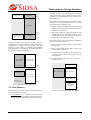
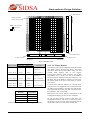
4.2.2. Data transfer (through SFR area)
Data transfer and fast control (such as the start
command and the end of conversion signals) are
mapped in the SFR area.
Locations $D8 through $DF, $E1 and $FF are used
(as shown in Table 4.8).
SFR
Register Name
Access mode
$D8 to $DB
$DC to $DF
$E1
DANA1 to DANA4
DANA5 to DANA8
ANAST (mPCONV[3:0])
ANAST (mPDONE[3:0])
outCOMP[3:0]
Read and write
Read Only
Read
Write
Read Only
$FF
Table 4.8: Logical Configuration Memory Organization selection
ü Input registers for ther DACs are written by
accessing to DANA1 to DANA4 SFRs.
ü Output registers from the ADCs may be
obtained by reading these four registers (DANA1 to
DANA4).
ü DANA5 to DANA8 are read only registers and
they are used in 4 input-multiplexed 10-bits ADC
mode (see CAB document for detailed description).
ü Outputs of the comparators section may be read
by accessing to the least significant nibble of the
read only OutCOMP SFR.
ü ANAST registers has different functions:
Writing on its bits, the corresponding ADC channel
starts conversion. With a read access to the register,
the end-of-conversion status is obtained. Only the
least significant nibble is used.
See CAB Document for further information
Locations
Internal
External*
Q0, $30
$00
Q0, $31
$01
Q0, $32
$02
Q0, $33
$03
Q0, $34
$08
Hardware Probing Mode
Horizontal 8-bit **
Vertical 8-bit ***
(1,0) & (0,0), comb
(0,1) & (0,0), comb
(3,0) & (2,0), comb
(0,3) & (0,2), comb
(5,0) & (4,0), comb
(0,5) & (0,4), comb
(7,0) & (5,0), comb
(0,7) & (0,6), comb
(1,1) & (0,1), comb
(1,1) & (1,0), comb
Hardware writing Mode
Horizontal 8-bit **
Vertical 8-bit ***
(1,0)&(0,0), context #0 (0,1)&(0,0) context #0
(3,0) & (2,0), ctx #0
(0,3) & (0,2), ctx #0
(5,0) & (4,0), ctx #0
(0,5) & (0,4), ctx #0
(7,0) & (5,0), ctx #0
(0,7) & (0,6), ctx #0
(1,1) & (0,1), ctx #0
(1,1) & (1,0), ctx #0
Q0, $4F
Q0, $50
$3B
$80
(7,7) & (6,7), comb
(1,0) & (0,0), seq
(7,7) & (7,6), comb
(0,1) & (0,0), seq
(7,7) & (6,7), ctx #0
(1,0) & (0,0), ctx #1
(7,7) & (7,6), ctx #0
(0,1) & (0,0), ctx #1
Q0, $6F
Q1, $30
$BB
$04
(7,7) & (6,7), seq
(9,0) & (8,0), comb
(7,7) & (7,6), seq
(1,8) & (0,8), comb
(7,7) & (6,7), ctx #1
(9,0) & (8,0), ctx #0
(7,7) & (7,6), ctx #1
(1,8) & (0,8), ctx #0
Q1, $4F
Q1, $50
$3F
$84
(15,7) & (14,7), comb
(9,0) & (8,0), seq
(7,15) & (6,15), comb
(1,8) & (0,8), seq
(15,7) & (14,7), ctx #0
(9,0) & (8,0), ctx #1
(7,15) & (6,15), ctx #0
(1,8) & (0,8), ctx #1
Q1, $6F
Q2, $30
$BF
$40
(15,7) & (14,7), seq
(1,8) & (0,8), comb
(7,15) & (6,15), seq
(9,0) & (8,0), comb
(15,7) & (14,7), ctx #1
(1,8) & (0,8), ctx #0
(7,15) & (6,15), ctx #0
(9,0) & (8,0), ctx #0
Q2, $4F
Q2, $50
$7B
$C0
(7,15) & (6,15), comb
(1,8) & (0,8), seq
(15,7) & (14,7), comb
(9,0) & (8,0), seq
(7,15) & (6,15), ctx #0
(1,8) & (0,8), ctx #1
(15,7) & (14,7), ctx #0
(9,0) & (8,0), ctx #1
Q2, $6F
Q3, $30
$FB
$44
(7,15) & (6,15), seq
(9,8)&(8,8), comb
(15,7) & (14,7), seq
(9,8)&(8,8), comb
(7,15) & (6,15), ctx #1
(9,8)&(8,8), ctx #0
(15,7) & (14,7), ctx #1
(9,8)&(8,8), ctx #0
Q3, $4F
Q3, $50
$7F
$C4
(15,15)&(14,15) comb
(9,0)&(8,15), seq
(15,15)&(14,15) comb
(9,0)&(8,15), seq
(15,15)&(14,15) ctx #0
(9,0)&(8,15), ctx #1
(15,15)&(14,15) ctx #0
(9,0)&(8,15), ctx #1
Q3, $6F
$FF
(15,15)&(14,15), seq
(15,15)&(14,15), seq
(15,15)&(14,15) ctx #1 (15,15)&(14,15), ctx #1
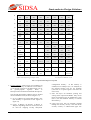
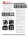
* Memory Locations are relative (absolute values depend on map organization version)
** DMCs are arranged to, first, from East to West and, secondly, from South to North of die size (8x8 for each Quarter in
internal access and 16x16 for external access)
*** DMCs are arranged to, first, from South to North and, secondly, from East to West of die size (8x8 for each Quarter in
internal access and 16x16 for external access)
Table 4.9: DMC association in vertical and horizontal accesses
Chapter 4. On-Chip Subsystems Interface
13