1
SIDSA
Auxiliary Memory
External
$FFFF
$FF00
$FEFF
Semiconductor Design Solutions
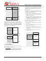
of RAM, the upper 128 bytes RAM area, 128 bytes
of special function register (SFR) area and 64 bytes
(located in $30 through $6F) of the buffer access
space (figure 1.2).
Both SFR area–upper RAM and lower RAM–buffer
access share the same addresses locations, so they
must be accessed in different ways:
External
a) SFR area and upper RAM are accessed trough
different addressing modes (direct and indirect
addressing, respectively)
Internal ROM
(Boot Program)
$0200
$01FF
External
$0000
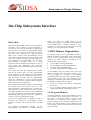
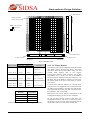
Fig. 1.1: Program Memory Address Space
256 bytes random access memory (auxiliary memory)
is provided in the upper addresses space and may be
simultaneously mapped in both program and data
memories. If this memory is enabled, location $FF00
through $FFFF are fetched from it (see Microprocessor
Document for further information).
$FF
Special Function
Register Area
Upper 128 bytes
Internal RAM
(direct addresing)
(indirect addresing)
b) The scratch pad area located in positions $30
through $6F may be disabled in order to access
to the buffer access area (only one of these two
memories may be enabled at a time)
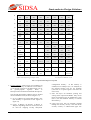
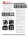
The lower 128 bytes are grouped in four addresses
space (as shown in figure 1.3):
a) Four General Purpose Registers banks ($00
through $1F),
b) Next 16 bytes ($20 through $2F) contains 128
directly addressable bits,
c) Location $30 through $6F can be used either as
a scratch pad area or as buffer access area (as
shown below)
d) Location $70 through $7F can be used as a
scratch pad area.
Scratch Pad Area
$80
$7F
$70
$6F
$7F
$6F
Buffer Access Area
Scratch Pad Area
Buffer Access
$30
Lower 128 bytes
Internal RAM
$30
Bit-addressable Area
Both direct and
indirect addressing
$00
Fig. 1.2: Data Memory / SFR Address Spaces
1.2. Data Memory
The Data Memory address space consists of an internal
and external memory portion.
$2F
$20
$1F
4 Banks for
General Purpose
Registers
$00
Fig. 1.3: Lower portion of the Internal Data Memory
• Internal Memory: It is divided into four physically
separated blocks (original 8051 internal memory is
only divided into three blocks): the lower 128 bytes
Chapter 4. On-Chip Subsystems Interface
3