1
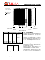
SIDSA
8051 Port 3.
Address
Name
PORTD
NRD
System Control Register 2 (h00 after Reset)
Description
8051 Port 3
PORTD.7
NRD for external memory. Must
not be cleared
NWR
PORTD.6
NWR for external memory.
Must not be cleared
PRTD5..2
5 thru 2
General Purpose
TXD
PRTD.1
(Output) Serial port TX
ETXD
PRTD.0
If cleared (=0), TX serial port is
enabled.
RX
PRTD.0
(Input) Serial Port RX
Note: Different registers are used for both read and write accesses.
While writing, b11 - - - - 10 must be fixed to keep communications
though the serial port.
$B0
Semiconductor Design Solutions
Bit
Address
$FD
Name
RG2
EPM
WPM
NPM
SPM
HOA1
Bit
RG2.7
RG2.6
RG2.5
RG2.4
RG2.3
HOA0
RG2.2
AME
RG2.1
EDMF
RG2.0
System Control Register 1 (h00 after Reset)
Address
$FC
Name
RG1
CQDB1
CQDB0
AMI
RG1.7
RG1.6
RG1.5
LMI
RG1.4
HOI
Bit
RG1.3
HOE
RG1.2
CMI
RG1.1
CME
RG1.0
Description
FIPSOCs Control Register 1
Chip Quarter Data Buffer bit 1.
Chip Quarter Data Buffer bit 0
Analog Configuration memory
mapped as Int. Mem. If 1,
configuration
memory
is
mapped in the Data Buffer
locations of the Internal Memory
($30-$6F)
LUT Data Memory mapped as
Internal Mem. If 1, LUT Data
memory is mapped in the Data
Buffer locations of the Internal
Memory ($30-$6F)
Hardware Outputs mapped as
Internal Memory. If 1, hardware
outputs are mapped in the Data
Buffer locations of the Internal
Memory
($30-$6F).
Use
CQDB1 and CQDB0 to select
the appropriate Quarter.
Hardware Outputs mapped as
External Memory
Configuration Memory mapped
as Internal Memory. If 1,
configuration
memory
is
mapped in the Data Buffer
locations of the Internal Memory
($30-$6F)
Configuration Memory mapped
as External Memory.
System Control Register 3 (h02 after Reset, 12x8
device)
Address
$9B
Name
RG3
Bit
INTM
RG3.7
RG3.6
RG3.5
RG3.4
RG3.3
RG3.2
CM1
RG3.1
CM0
RG3.0
Description
FIPSOCs Control Register 3
Description
FIPSOCs Control Register 2
East Pads Mask bit.
West Pads Mask bit
North Pads Mask bit
South Pads Mask bit.
Hardware Outputs Access Mode
1.
Hardware Outputs Access Mode
0.
Auxiliary Memory Enable. If this
bit is set, the Aux. memory
(256x8bits) is mapped at
locations $FF00-$FFFF of both
external data and program
memories.
External Data Memory Function.
If 1, external data memory is
mapped in program memory
locations. If this bit is set and
CME = 1, the configuration
memory of the Programmable
Logic is used both for data and
program memories .
Transfer Command Register (h2F after Reset)
Address
$FE
Name
RGTX
PLTB
Bit
RGTX.7
CTXSB
RGTX.6
FCB
RGTX.5
FAB
RGTX.4
Description
Transfer Register
Programmable Logic Transfer
bit. Writing to RGTX with this
bit set produce a context transfer
(set by RGTX.6) of the
configuration in the DMCs
Context Select Bit. If this bit is
set when writing to RGTX with
PLTB = 1, context 1 is
transferred to the configuration
memory of the selected DMCs.
If this bit is 0, context 0 is
transferred.
Freezing Command Bit. A
writing to RGTX with this bit set
produce an start/stop action in
the state machine of the clock
generation block.
Freezing Action Bit. If this bit is
set when writing to RGTX with
FCB = 1, clocks stops by SW
after CKCNT. If 0, clocks
restarts.
RGTX.3
RGTX.2
RGTX.1
RGTX.0
Interrupt mode. If 1, extended
interrupt vectors mode is
entered, if 0, basic 8051
interrupt mode is selected
External Memory Compatible
map bit 1
External Memory Compatible
map bit 0
Chapter 4. On-Chip Subsystems Interface
8