1
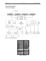
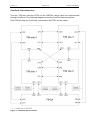
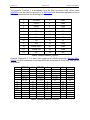
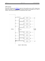
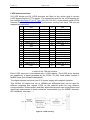
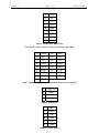
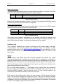
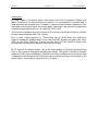
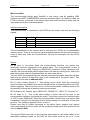
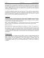
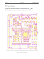
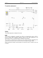
SMT148
User Manual
Sundance Digital Signal Processing Inc
4790 Caughlin Parkway #233, Reno, NV 89509-0907, USA.
Version 1.4
Page 2 of 35
SMT148 User Manual
Revision History
Date
Comments
Engineer
Version
31/03/2004
First release
PV
1.0
26/10/2004
Added power consumption
GP
1.1
02/11/2004
Power connector part numbers clarified.
GP
1.2
08/03/2006
Removed textual references to VP20
GP
1.3
30/08/2006
JTAG header pinout corrected
SM
1.4
Version 1.4
Page 3 of 35
SMT148 User Manual
Table of Contents
Revision History.......................................................................................................... 2
List of abbreviations.................................................................................................... 5
Introduction................................................................................................................. 6
Overview ................................................................................................................. 6
Related Documents ................................................................................................ 6
General Description.................................................................................................... 7
Carrier block diagram.............................................................................................. 7
ComPorts interconnections ..................................................................................... 8
Global Bus connections ........................................................................................ 10
DAC circuitry ......................................................................................................... 10
ADC circuitry ......................................................................................................... 11
LVDS drivers/receivers ......................................................................................... 12
32-bit microcontrollers........................................................................................... 13
RS485 ................................................................................................................... 15
RSL ....................................................................................................................... 15
SHB ...................................................................................................................... 15
Power supplies...................................................................................................... 16
Power in ............................................................................................................ 16
Power Consumption .......................................................................................... 16
Power out .......................................................................................................... 17
JTAG..................................................................................................................... 17
LED ....................................................................................................................... 17
Fan Power............................................................................................................. 17
Reset Scheme ...................................................................................................... 17
IIOF Connectivity .................................................................................................. 18
FPGA configuration............................................................................................... 18
FPGA Firmware description...................................................................................... 19
Switch Fabric ........................................................................................................ 20
Input node (source) ........................................................................................... 21
Output node (destination) .................................................................................. 21
ComPorts (x8)....................................................................................................... 21
Source ............................................................................................................... 21
Destination ........................................................................................................ 22
Microcontroller ...................................................................................................... 23
Interface description .......................................................................................... 23
Source ............................................................................................................... 23
Destination ........................................................................................................ 24
Version 1.4
Page 4 of 35
SMT148 User Manual
Polling interrupts................................................................................................ 24
Registers and address mapping........................................................................ 25
Watchdog timers ................................................................................................... 27
Reset..................................................................................................................... 27
DAC ...................................................................................................................... 28
ADC ...................................................................................................................... 29
LED ....................................................................................................................... 30
RSL ....................................................................................................................... 30
SHB ...................................................................................................................... 30
RS485 ................................................................................................................... 30
Global Bus and McBSP......................................................................................... 31
Verification Procedures ............................................................................................ 31
Review Procedures .................................................................................................. 31
PCB Layout Details .................................................................................................. 32
Connectors placement.............................................................................................. 33
Safety ....................................................................................................................... 33
EMC ......................................................................................................................... 33
Getting started with the SMT148 .............................................................................. 34
Connection to the host .......................................................................................... 34
JTAG connection ............................................................................................... 34
External ComPort cable..................................................................................... 34
SMT148 interconnection ....................................................................................... 34
Checking that the system is functional .................................................................. 34
Running your first application on the SMT148 ...................................................... 35
Updating the FPGA firmware or the microcontroller boot code................................. 35
Version 1.4
Page 5 of 35
List of abbreviations
ADC
DAC
DSP
EPROM
FPGA
JTAG
LED
LSB
LVDS
MSB
RSL
SDB
SHB
SPI
TIM
UART
USB
Analog to Digital Converter
Digital to Analog Converter
Digital Signal Processing
Erasable Programmable Read-Only Memory
Field Programmable Gate Array
Join Test Action Group
Light Emitting Diode
Least Significant Bit(s)
Low Voltage Differential Signaling
Most Significant Bit(s)
Rocket IO Sundance Link
Sundance digital bus
Sundance High-speed Bus
Serial Peripheral Interface
Texas Instrument Module
Universal Asynchronous Receiver Transmitter
Universal Serial Bus
SMT148 User Manual
Version 1.4
Page 6 of 35
SMT148 User Manual
Introduction
Overview
The SMT148 is a four sites TIM carrier board with external interfaces
Connectors are provided to interface to:
•
Analog inputs (x8)
•
Analog outputs (x8)
•
UART (RS485)
•
UART (RS232) (x2)
•
LVDS (56 pairs)
•
JTAG
•
RSL
•
SHB
•
RS485 (16 pairs)
•
USB (x2)
•
Firewire (1394b) (x2)
•
LED (x32)
Related Documents
Texas Instruments Module specification
External Interface User Manual: this document gathers all the functionalities of the
Sundance’s firmware implemented on DSP TIMs
SMT118: Carrier with 3 Module sites and I/O facilities
SMT180: Carrier with 8 Module sites
Version 1.4
Page 7 of 35
General Description
Carrier block diagram
Figure 1: Carrier block diagram
Interface
ADC
DAC
UART
LVDS
RSL
SHB
RS485
USB
Firewire
LED
TIM global bus
connections
TIM ComPorts
XC2VP7
optional
yes
yes
yes
optional
half, optional
optional
optional
optional
yes
yes(20 pins)
yes (4)
Table 1 : Interfaces
SMT148 User Manual
Version 1.4
Page 8 of 35
SMT148 User Manual
ComPorts interconnections
The four TIM sites and the FPGA on the SMT148 carrier card can communicate
through ComPorts. The following diagram shows the ComPort interconnections.
Each TIM site has two ComPorts connected to the FPGA on the carrier.
Figure 2 : ComPorts interconnection
Version 1.4
Page 9 of 35
SMT148 User Manual
The external ComPort_1 is accessible on a 26 Way connector (3M), which cable
(SMT502) can be used to connect to a SMT310Q and download application from a
PC. This connector has the following pin-out.
1
CSTRB
2
GND
3
CRDY
4
GND
5
CREQ
6
GND
7
CACK
8
GND
9
D0
10
D1
11
D2
12
D3
13
D4
14
D5
15
D6
16
D7
17
3.3V
18
GND
19
/RESETOUT
20
GND
21
/RESETIN
22
GND
23
NC
24
NC
Table 2 : External ComPort_1 pinout
External Comports 2, 3, 4 and 5 are routed to two SHB connectors (Samtec QSH030-01) to allow connection to another SMT148 carrier and its ComPorts. The pin-out
is as follow:
1
5
9
13
17
21
25
29
33
37
41
45
49
53
57
CSTRB_CP2
D0__CP2
D4__CP2
NC
CREQ_CP3
D2_CP3
D6_CP3
CSTRB_CP4
D0_CP4
D4_CP4
NC
CREQ_CP5
D2_CP5
D6_CP5
NC
2
6
10
14
18
22
26
30
34
38
42
46
50
54
58
CRDY_CP2
D1_CP2
D5_CP2
NC
CACK_CP3
D3_CP3
D7_CP3
CRDY_CP4
D1_CP4
D5_CP4
NC
CACK_CP5
D3_CP5
D7_CP5
NC
3
7
11
15
19
23
27
31
35
39
43
47
51
55
59
CREQ_CP2
D2_CP2
D6_CP2
CSTRB_CP3
D0__CP3
D4_CP3
NC
CREQ_CP4
D2_CP4
D6_CP4
CSTRB_CP5
D0_CP5
D4_CP5
NC
NC
Table 3 : External ComPorts 2-5 pinout
4
8
12
16
20
24
28
32
36
40
44
48
52
56
60
CACK_CP2
D3_CP2
D7_CP2
CRDY_CP3
D1_CP3
D5_CP3
NC
CACK_CP4
D3_CP4
D7_CP4
CRDY_CP5
D1_CP5
D5_CP5
NC
RESET
Version 1.4
Page 10 of 35
SMT148 User Manual
Global Bus connections
Some of the Global bus signals from the TIM sites are connected point-to-point to the
FPGA on the SMT148 carrier card.
These 19-bit data communication links can be used for different purposes (McBSP,
HPI, interrupts …) and any protocol could be implemented in order to meet specific
requirements. The firmware in the FPGA will make use of these links to give more
flexibility to the system and thus balance the data/control load on the carrier
depending on the customer constraints.
DAC circuitry
The SMT148 comprises eight 16-bit low-speed DAC channels with a ±10V output
voltage span (DAC7742, 200kSPS/channel max) and internal voltage reference. See
firmware description for details about DAC control.
Figure 3 : DAC circuitry
Version 1.4
Page 11 of 35
SMT148 User Manual
ADC circuitry
Eight ADC channels (8x AD7899-1) with a 14-bit resolution and a ±10V voltage input
span are available on the SMT148.The analog inputs can be sampled up to a rate of
400kHz. See firmware description for details about DAC control.
Figure 4 : ADC circuitry
Version 1.4
Page 12 of 35
SMT148 User Manual
LVDS drivers/receivers
24 LVDS drivers and 24 LVDS receivers are fitted on the carrier card to convert
LVDS signals from/to LVTTL signals. The connectors used for the LVDS signals are
four straight NorComp 37-pin D Type (191-037-113-001). In the default carrier FPGA
firmware implementation two McBSP connections coming from each TIM site are
mapped per connector.
GND
Input/Output
20
GND
2
McBSP_CLKR_Tx_0+
I
21
McBSP_CLKR_Tx_0-
3
McBSP_FSR_Tx_0+
I
22
McBSP_FSR_Tx_0-
4
McBSP_DR_Tx_0+
I
23
McBSP_DR_Tx_0-
5
GND
1
24
GND
6
McBSP_CLKX_Tx_0+
O
25
McBSP_CLKX_Tx_0-
7
McBSP_FSX_Tx_0+
O
26
McBSP_FSX_Tx_0-
8
McBSP_DX_Tx_0+
O
27
McBSP_DX_Tx_0-
28
GND
9
GND
10
GND
11
GND
29
GND
12
McBSP_CLKR_Tx_1+
I
30
McBSP_CLKR_Tx_1-
13
McBSP_FSR_Tx_1+
I
31
McBSP_FSR_Tx_1-
14
McBSP_DR_Tx_1+
I
32
McBSP_DR_Tx_1-
15
GND
33
GND
16
McBSP_CLKX_Tx_1+
O
34
McBSP_CLKX_Tx_1-
17
McBSP_FSX_Tx_1+
O
35
McBSP_FSX_Tx_1-
18
McBSP_DX_Tx_1+
O
36
McBSP_DX_Tx_1-
19
GND
37
GND
Table 4: LVDS pinout (default firmware)
x refers to the TIM site number.
Each LVDS input pair is terminated with a 100Ω resistor. The LVDS driver devices
are enabled by a signal generated by the FPGA (TX_EN), each enable controls 2
McBSP ports (see firmware description).
The digital isolators have their own 3.3V power supply with magnetic isolation.
This 4.8Gb/s full duplex link (up to 100Mb/s per differential pair) can be used for
different purposes that require LVDS on the external world for long distance
communications. Data transfers and their associated protocol can be performed and
specifically implemented to meet customers’ requirements (e.g. 4x McBSP channels,
SPI interfaces, interrupts …).
Figure 5 : LVDS circuitry
Version 1.4
Page 13 of 35
SMT148 User Manual
32-bit microcontrollers
The FPGA on the SMT148 carrier card is connected to two 32-bit microcontrollers
(oxuf922) that enable communication with some of the most widely used standards:
UART (RS485, RS232), USB, and Firewire (1394b). Data transfers and instructions
can be set between the microcontrollers and the FPGA in both directions thus
allowing the implementation of many different schemes. The flash device will hold the
FPGA and microcontroller firmware. The 48MHz clock is required for the use of the
USB. Each microcontroller will have the following interfaces. The second
microcontroller interfaces only to a USB connector, RS232 and the FPGA.
The microcontrollers are accessible through a JTAG connector (JP10). This is the
only device in this chain. The pinout is as follow:
1
3.3V
2
TRST
3
TCK
4
TMS
5
TDO
6
TDI
Table 5 : Microcontroller JTAG
Figure 6 : Microcontroller interfaces (uC1, U65)
A jumper (JP14) enables RS232 when inserted, RS485 when removed.
Version 1.4
Page 14 of 35
1
DCD
2
Rx
3
Tx
4
DTR
5
GND
6
DSR
7
8
RTS
CTS
9
RI
SMT148 User Manual
Table 6 : RS232 UART DB9 pinout
The RS232 cable needs to be a Null Modem cable DB9
1
DCD+
14
DCD-
2
Rx+
15
Rx-
3
Tx+
16
Tx-
4
DTR+
17
DTR-
5
DSR+
18
DSR-
6
19
7
RTS+
CTS+
20
RTSCTS-
8
RI+
21
RI-
9
GND
Table 7 : RS485 UART DB25 pinout (all other pins are not connected)
1
USB_ind
2
Data-
3
Data+
4
GND
Table 8 : USB pinout
1
NC
2
GND
3
TPB-
4
TPB+
5
TPA-
6
TPA+
Table 9 : Firewire pinout
Version 1.4
Page 15 of 35
SMT148 User Manual
RS485
16 bi-directional RS485 pairs are connected to the FPGA. Each byte direction is
controlled by the firmware. The RS485 driver/receivers are connected to a SDB type
connector (40 way). The connector pinout is as follow:
Function
S0S1S2S3S4S5S6S7GND
GND
pin
1
3
5
7
9
11
13
15
17
19
pin
2
4
6
8
10
12
14
16
18
20
Function
S0+
S1+
S2+
S3+
S4+
S5+
S6+
S7+
GND
GND
Function
GND
GND
S8S9S10S11S12S13S14S15-
pin
21
23
25
27
29
31
33
35
37
39
pin
22
24
26
28
30
32
34
36
38
40
Function
GND
GND
S8+
S9+
S10+
S11+
S12+
S13+
S14+
S15+
Table 10: RS485 pinout
RSL
A RSL link is available on the carrier and can allow users to transfer up to 20Gb/s of
data in full duplex mode. This ultra high speed transfer link uses the dedicated
Rocket IO from the Xilinx FPGA. Refer to RSL specifications and pinout for more
details.
SHB
One 60-pin SHB connector (Samtec QSH-030-01) is connected to the FPGA. It can
be used for debugging purposes and connected to a Logic Analyser using some
specific adapters.
It can also be used as a high speed link to transfer data to the FPGA carrier and TIM
modules using the SDB protocol (2x 200Mbytes/s). For this configuration, please
refer to SHB documentation.
Version 1.4
Page 16 of 35
SMT148 User Manual
Power supplies
Power in
Power is supplied from an external source. The voltage of the external source needs
to be in the range +18V +30V. This enters the board via an 8-pin connector (JP6 on
board, Receptacle, mini fit 8 Way, Molex 39-28-1083).
+18-30V
1
+18-30V
2
+18-30V
3
+18-30V
4
GND
5
GND
6
GND
7
GND
8
Table 11 : Power in pinout
The mating part to this connector is a Molex 39-01-2080 (Farnell order code 151-869
+ 8 off 39-00-0039, Farnell 151-890).
The external source is input to a DC-DC converter module, which produces +/-12V to
the TIM sites. It is also used as an input to two DC-DC converters that produce the
+5V, +3.3V, +2.5V and 1.5V supply to the TIM sites, carrier FPGA and other devices.
Power Consumption
The typical current consumption of an SMT148-LT would be 120mA at 24V. For an
SMT148, this would be 280mA.
These are actual measured values with no TIMs fitted.
When TIMs are added, then the power consumption of the TIMs must be added to
that of the SMT148/-LT with the SMT148 power supply efficiency taken into account
(approximately 80%).
Example:
Power consumption of SMT148-LT only = 24*0.12 = 2.88W
Power consumption of TIM, say 3.3V at 1A = 3.3W
Total power consumption = 2.88 + 3.3/0.80 = 7.0W
Version 1.4
Page 17 of 35
SMT148 User Manual
Power out
Power can be supplied to external devices or modules. The 8-pin connector
(Receptacle, mini fit 8 Way, Molex), providing different voltages, has the following
pinout:
Pin number
-12V
1
+12V
2
+5V
3
+3.3V
4
GND
5
GND
6
GND
7
GND
8
Table 12 : Power out pinout
JTAG
A single JTAG chain connects all 4 TIM sites and the JTAG in & out connectors. This
chain is used with the TI Code Composer Studio software suite.
The JTAG-out (JTAG2) connector can be connected to the JTAG-in (JTAG1)
connector of other SMT148, thus extending the chain (see cable SMT503).
LED
A 8x4 array of LED is connected directly to the FPGA and is controlled by the FPGA
firmware
Fan Power
Eight two-pin connectors are provided to supply fans with a +12V supply.
Reset Scheme
A power rail monitor observes the state of the 3.3V supply. This device will generate
a reset to the SMT148 (RESET148) during power-up or if the 3.3V supply drops
below 3V. This signal is an open-collector output and is also driven to the inter-card
ComPort connector, and thus to another SMT148.
The POR (power on reset) signal is driven to the RESETOUT pin on the external
ComPort1 connector. The RESETIN pin on the above connector is buffered by an
open-collector device which in turn can also drive the RESET148 signal. An
additional 4 pin header is provided to allow other devices to share the open-collector
RESET148 signal.
The TIM reset pins are connected to the FPGA and will be reset when RESET148 is
active as well as when some firmware conditions trigger a reset to the different TIMs
(see Firmware description for more details about TIM reset).
Version 1.4
Page 18 of 35
SMT148 User Manual
IIOF Connectivity
Each TIM site provides 3 interrupt pins, IIOF0, 1 & 2.
IIOF0 & 1 are connected in a daisy-chain with TIM site 1 IIOF0 connected to TIM site
2 IIOF1; TIM site 2 IIOF0 connected to TIM site 3 IIOF1 finishing with TIM site 4
IIOF0 connected to TIM site 1 IIOF1.
All TIM site’s IIOF2 signals are connected together.
FPGA configuration
In the default configuration the FPGA is configured by the microcontroller that fetches
the configuration in the flash device. However it is possible to download a new
configuration to the FPGA using the Xilinx JTAG cable connected to a PC and to JP5
on the SMT148 carrier. The pinout is as follow:
1
3.3V
2
GND
3
TMS
4
TCK
5
TDI
6
TDO
Table 13 : FPGA configuration
Version 1.4
Page 19 of 35
SMT148 User Manual
FPGA Firmware description
The FPGA Virtex II Pro on the SMT148 carrier card is connected to many different
devices and therefore has many internal interfaces that allow it to exchange data or
commands with the external world. All interfaces are reset at power on or when a
manual reset is applied. The diagram below shows the interconnections between the
digital modules inside the FPGA.
Figure 7 : FPGA firmware
Version 1.4
Page 20 of 35
SMT148 User Manual
Switch Fabric
Due to the high number of interfaces to be implemented in the firmware it is important
to keep the design scalable and flexible. The switch fabric is a digital component that
could be seen as a giant multiplexer/demultiplexer and that allows to dynamically
connect the different interfaces to each others. The switch fabric will run on the
FPGA system clock (100MHz by default) and will therefore not become the
bottleneck for any transfer. It has multiple input nodes and output nodes operating
under a protocol disregarding the specificities of the interfaces it is connected to. The
node data/address bus is 8-bit wide plus few control signals. Any input node can
target any output node but one input node can be remotely connected to only one
output node at a time. When a transfer is about to be started by a specific interface
(input node) the first word received on the switch fabric input node will be the address
of the output node it needs to access. Three bytes of zeros will then be sent after the
address byte. The data/address/control words that will follow will be sent to the
output node and must comply with the specific format of the targeted interface.
Output node
ComPort_0 (TIM1)
ComPort_1 (TIM1)
ComPort_2 (TIM2)
LED
ComPort_4 (TIM3)
DAC
ComPort_6 (TIM4)
μcontroller1
McBSP TIM1
McBSP TIM2
McBSP TIM3
McBSP TIM4
Watchdog timer TIM1
Watchdog timer TIM2
Watchdog timer TIM3
Watchdog timer TIM4
RS485
μcontroller2
RSL
SHB
ComPort_3 (TIM2)
ComPort_5 (TIM2)
ComPort_7 (TIM2)
ADC
Switch Fabric
Address (Hex)
00
01
02
03
04
05
06
07
08
09
0A
0B
0C
0D
0E
0F
10
11
12
13
14
15
16
17
F0
Table 14 : Output nodes addresses
Version 1.4
Page 21 of 35
SMT148 User Manual
Input node (source)
The input node is defined as being an input to the switch fabric. It runs on the FPGA
system clock and has the following input and output signals.
WE
HOLD
DATA
input
output
input
Write enable
Receiver is full or already busy with another node, hold transfer
8-bit data bus
Table 15: Input node IO
Note that all transfers are made in burst of 4 words. Therefore the HOLD flag should
be taken into account when the burst is completed.
Output node (destination)
The output node is an output from the switch fabric. It runs on the FPGA system
clock and has the following input and output signals.
WE
FULL
DATA
DONE
output
input
output
input
Write enable
Receiver full, transmitter must hold transfer
8-bit data bus
Transfer completed
Table 16 : Output node IO
The output node interface, depending on the settings and data it received, and
detecting that the transfer is completed will assert a completion signal (DONE) to the
switch fabric that will disable the connection between the two nodes.
ComPorts (x8)
The ComPorts interfaces are directly connected to the switch fabric and allow
communication with external devices and modules using the ComPort or SDL
protocol (please refer to the SDL Technical Specifications for more details). On the
switch fabric side the ComPorts must comply with the input and output node
descriptions.
Source
As an input to the switch fabric the ComPort interface can access any output
resources (destinations) connected to the switch fabric. To enable the connection to
a specific destination the ComPort interface must send the right address to the switch
fabric and once connected can start streaming data and/or control to the output node.
The ComPort source to the switch fabric also expects one 32-bit word before it can
start sending data to the switch fabric:
Bit 31: never ending transfer if 1. This setting can be useful when the connection
needs to always be enabled such as the DSP is streaming data to the DAC via the
ComPort without stopping. This bit must be set to 0 if the ComPort needs to be
dynamically reconnected to another node at some stage.
Bit 23 down to 0: transfer length. This is the total number of 32-bit words that will be
sent to the ComPort interface (excluding this word). This gives a maximum transfer
length of 2^26-4 bytes (64Mbytes). When the ComPort interface has received all data
it expected, it will go in an idle state for 2us before starting a new transfer if instructed
to do so. This setting is ignored if bit 31 is set to 1.
Version 1.4
Page 22 of 35
SMT148 User Manual
Destination
Any input node to the switch fabric can access the ComPort interface. Please note
that a ComPort is a bi-directional bus. However it is not possible to transfer data in
both directions at the same time. Therefore, if some activity has been detected on the
input path to the switch fabric, the output path, if accessed, will raise its full flag when
it cannot accept data anymore (i.e., when its FIFO is full).
The ComPort interface must first receive a 32-bit word of settings In order to be able
to start transmitting the data it will receive.
Bit 31: never ending transfer if 1. This setting can be useful when the connection
needs to always be enabled such as the case the ADC streams its data to the same
DSP via one of his ComPorts. This bit must be set to 0 if the ComPort needs to be
dynamically reconnected to another node at some stage.
Bit 23 down to 0: transfer length. This is the total number of 32-bit words that will be
sent to the ComPort interface (excluding this word). This gives a maximum transfer
length of 2^26-4 bytes (64Mbytes). When the ComPort interface has received all data
it expected it will disconnect itself from the input node by sending a done pulse to the
switch fabric. This setting is ignored if bit 31 is set to 1.
Version 1.4
Page 23 of 35
SMT148 User Manual
Microcontroller
The microcontroller brings great flexibility to this carrier card by enabling USB,
Firewire and UART (RS485/RS232) external communications. Its interface inside the
FPGA is directly connected to the switch fabric and must therefore comply with the
input node and output node descriptions.
Interface description
The microcontroller is connected to the FPGA on the carrier card with the following
signals:
DATA
ADDRESS
NWE
NOE
NCS2
input/output
input
input
input
input
8-bit data bus, bidirectional
12-bit address bus
Write enable, active low
Output enable, active low
Chip select, active low
The microcontroller is the master device and sees the FPGA as an addressable
memory space. There is no interrupt signal available between the two devices and in
order to catch any event the microcontroller will poll the interrupts from the FPGA
regularly.
Source
As an input to the switch fabric the microcontroller interface can access any
destination resource connected to the switch fabric. The microcontroller is able to
convey data from a USB, Firewire or RS485/232 connection. When initiating a new
transfer, the microcontroller should signal where the data are coming from, how much
data there is and what the final destination for these data will be.
The first 32-bit word expected by the interface contains information about the transfer
type and the amount of data that need to be transferred to the switch fabric. This
word needs to be sent to address h000
Bit 31: never ending transfer if 1. This setting can be useful when the connection
needs to always be enabled such as the microcontroller is streaming data to the DAC
without stopping. This bit must be set to 0 if the microcontroller interface needs to be
dynamically reconnected to another node at some stage.
Bit 29 down to 28: Transfer type, RS232=”00”, RS485=”01”, USB=”10”, Firewire=”11”
Bit 25 down to 0: This is the total number of bytes that will be sent to the
microcontroller interface (excluding this word). This gives a maximum transfer length
of 2^26-1 bytes (64Mbytes). When the microcontroller interface has received all data
it expected, it will go in an idle state for 2us before starting a new transfer if instructed
to do so. This setting is ignored if bit 31 is set to 1.
Please note that all nodes connected to the switch fabric transmit and receive
information based on 32-bit words. All the remaining words part of this transfer will be
sent to address h001.
The second 32-bit word sent to the interface and passed to the switch fabric is the
destination address (coded on the LSB, all other bytes must be set to 0). It can
Version 1.4
Page 24 of 35
SMT148 User Manual
happen that the microcontroller is not aware of the destination of the data it passes to
the FPGA. If the address sent is 255 (hFF), the interface will fetch the value of a
specific register that can be set by any resource in the system (see destination
register). This register will contain the address of the destination and will be passed
to the switch fabric if required.
In RS232 and RS485 modes, only one byte (the 1st byte, LSB) of relevant data is
transferred by 32-bit words. This has no implication on the firmware. However users
who for example write a program to be executed on DSP TIM to receive or transmit
data from/to the microcontroller should bear this in mind!
Destination
The microcontroller can be accessed by any resource connected to the switch fabric.
It offers the option of streaming data over USB, Firewire, RS485 or RS232. The first
32-bit word this node will receive will describe the type of transfer it needs to perform
as well as how much data will be transferred.
Bit31: never ending transfer if 1. This bit must be set to 0 if the microcontroller
interface needs to be dynamically reconnected to another node at some stage.
Bit 30: must be 0
Bit 29 down to 28: Transfer type, RS232=”00”, RS485=”01”, USB=”10”, Firewire=”11”
Bit 23 down to 0: This is the total number of 32-bit words that will be sent to the
microcontroller interface (excluding this word). This gives a maximum transfer length
of 2^26-4 bytes (64Mbytes). When the microcontroller interface has received all data
it expected from the switch fabric it will disconnect itself automatically by sending a
done pulse.
Polling interrupts
The microcontroller is a master over the FPGA. It needs to check regularly what the
status of the different resources inside the microcontroller interface is. Note that a
status request can be performed at any time during a transfer from the
microcontroller to the interface. However a status request during an interface to
microcontroller transfer can only be performed when a 32-bit word transfer is
complete.
Version 1.4
Page 25 of 35
SMT148 User Manual
Registers and address mapping
In addition to being written and read for data transfers, the microcontroller interface
includes some registers that can be accessed or written by the microcontroller:
Register/command
Address
(Hex)
Settings write
000-003
Write data
004-007
Read data
008-00B
Destination register (read)
00C-00F
Destination register (write)
010-013
Status register (read)
014-017
Firmware revision number
018-01B
RAM (read/write)
800-FFF
Table 17 : Register addresses
When ordered to read a register the interface inside the FPGA will then be given the
bus and will shift out the required register to the microcontroller.
Version 1.4
Page 26 of 35
SMT148 User Manual
Status register
Bit 29 down to 28: Transfer type to microcontroller
RS232=”00”, RS485=”01”, USB=”10”, Firewire=”11”
Bit 9: Busy signal, active high. It indicates that the data path to the switch fabric is
busy with a transfer from the microcontroller. A new transfer from the microcontroller
cannot be started until this signal has been de-asserted.
Bit 8: FIFO to Switch Fabric almost full => the microcontroller should stop writing data
to the interface and wait for this flag to be low again before continuing the transfer.
Bit 7 down to 0: Number of words in the FIFO to the microcontroller (FIFO is 1024
words deep) => the microcontroller can start reading data with a maximum burst size
of this number.
Destination register
This register contains the address of the destination connected to the switch fabric
when the microcontroller does not know where to send the words it will transmit (i.e.,
when the microcontroller tries to access a node with address 255). The default value
of this register is h40000000 (ComPort 0). This register can be written or read by the
microcontroller using register addresses (Table 17). This register can also be written
by any node connected to the switch fabric (e.g., ComPorts) when sending the
following word to the microcontroller interface.
Bit 30: must be 1
Bit 7 downto 0: Address of the destination node
Firmware revision number
The firmware revision number can be accessed by the microcontroller in order to
check what are the version of the current firmware as well as the size of the FPGA.
The firmware revision number is coded on 8 bits.
Bit 31 down to 8: reserved
Bit 7 down to 5: a, revision number “before comma”
Bit 4 down to 2: b, revision number “after comma”
Bit 1 down to 0: c, FPGA size , 00=> VP7
Version 1.4
Page 27 of 35
SMT148 User Manual
Watchdog timers
The watchdog timers are used for reset purposes by the different TIM modules in the
system. Each TIM can access its own watchdog timer and set a time that will elapse
before the TIM or all TIM modules are reset.
The watchdog timer expects 4 words (of one byte each). The first byte received is the
LSB; the fourth byte is the MSB. After receiving these four words the watchdog timer
will send a DONE pulse to the switch fabric in order for the input node to be
disconnected.
The four bytes received by the watchdog timer accounts for a 32-bit word:
Bit 29: All TIM reset if 1, only one TIM reset if 0.
Bit 28 down to 0: number of clock cycles before reset. If this number has been set to
0, the watchdog timer is disabled. The watchdog timer can be programmed for 1
clock cycle (10ns) up to 2^29-1 cycles (5.3s).
Each watchdog timer can be interrupted any time by writing 4 bytes of 0 to it.
On the switch fabric side the watchdog timer is compliant to interface to an output
node. The watchdog timer also interfaces to the reset circuitry with the following
signals.
GRESET
TRESET
Output
Output
Global reset to all TIM
Reset one TIM only
Table 18 : Watchdog timer extra IO
Reset
The reset circuitry inside the FPGA is connected to the watchdog timers. When it
receives a GRESET pulse it will reset all TIM modules for 2^20 cycles (~10ms).
When it receives a TRESET pulse it will reset one TIM module for 2^20 cycles
(~10ms). The reset circuitry has the following inputs and outputs.
GRESET1
GRESET2
GRESET3
GRESET4
TRESET1
TRESET2
TRESET3
TRESET4
nTIM1RESET
nTIM2RESET
nTIM3RESET
nTIM4RESET
input
input
input
input
input
input
input
input
output
output
output
output
Global reset to all TIMs from watchdog timer 1
Global reset to all TIMs from watchdog timer 2
Global reset to all TIMs from watchdog timer 3
Global reset to all TIMs from watchdog timer 4
Reset TIM 1 from watchdog timer 1
Reset TIM 2 from watchdog timer 2
Reset TIM 3 from watchdog timer 3
Reset TIM 4 from watchdog timer 4
TIM1 reset, active low
TIM1 reset, active low
TIM1 reset, active low
TIM1 reset, active low
Table 19 : Reset IO
Version 1.4
Page 28 of 35
SMT148 User Manual
DAC
The DAC interface is only an output node to the switch fabric and it interfaces to the
DAC device on the carrier card. All eight channels are controlled and updated by this
interface. The DAC interface is a slave and will disconnect itself from the input node
only if it receives the instruction to do so.
To initialize a transfer or disconnect itself from the input node the DAC interface
expects to receive the following 32-bit word (4 consecutive bytes, LSB first):
Bit 31: new transfer initialization if 1.
Bit 30: disconnect from input node if 1, will result in a DONE pulse sent to the switch
fabric.
Bit 15 down to 8: sampling ratio. The DAC devices are converting data from digital to
analogue at a fixed rate of 200 KHz. However the user can reduce this converting
rate by a factor determined by the sampling ratio value. Example: if sampling ratio =
8, the new conversion rate is 200KHz/8=25KHz. Sampling ratio=0 Ù Sampling
ratio=1.
Bit 7 down to 0: Channels enable, 1 on bit X indicates that channel X will be used, 0
that it will not.
If the DAC interface received a new transfer initialization command, the next words
will be interpreted as samples. One sample is coded on 4 bytes, LSB received first.
Bit 31: must be 0 (otherwise interpreted as initialization)
Bit 30: must be 0 (otherwise interpreted as disconnection)
Bit 23 down to 16: channel to which the sample belongs, 1 on bit X indicates that the
sample belongs to channel X-16. All the other bits must be set to 0.
Bit 15 down to 0: sample value
The DAC interface communicates to the DAC device on board using the following
signals. Please refer to the DAC7742 datasheet for more details.
RnW
nCS
nLDAC
RSTSEL
nRST
nREFEN
Data_to_dac
output
output
output
output
output
output
output
Read, not Write
8-bit chip select, active low, one nCS per channel
Load DAC register to output, active low
Tied to 1, output is half-scale code when DAC reset
Reset, active low
Enables internal +10V reference, active low
16-bit data bus
Table 20 : DAC interface extra IO
Version 1.4
Page 29 of 35
SMT148 User Manual
ADC
The ADC interface is an input as well as an output node to the switch fabric. All eight
channels are controlled by this interface. It needs to receive settings before it can
transmit digitized samples to the interface it was initialized by.
To initialize a transfer or disconnect itself from the input node the ADC interface
expects to receive the following 32-bit word (4 consecutive bytes, LSB first):
Bit 31: new transfer initialization if 1.
Bit 30: disconnect from input node if 1, will result in a DONE pulse sent to the switch
fabric.
Bit 23 down to 16: output node address to which the digitized samples will be sent to
Bit 7 down to 0: Channels enable, 1 on bit X indicates that channel X will acquire
data, 0 that it will not.
After the ADC interface has been initialized it will start transmitting the digitized
samples through the switch fabric to the specified output node.
The first 32-bit word sent from the ADC interface to the switch fabric will address the
output node it needs to access.
Bit 31 down to 8: set to 0
Bit 7 down to 0: output node address (see table 14)
The next words sent to the switch fabric will have the following format:
Bit 31 down to 24: time stamp. This value is incremented by one every time a new
sample is available on a specific channel. If the receiver detects that 2 samples from
the same channel received consecutively have a time stamp difference not equal to
one, this means that some samples have been lost during transfer.
Bit 23 down to 16: channel to which the sample belongs, 1 on bit X indicates that the
sample belongs to channel X-16. All the other bits will be set to 0.
Bit 13 down to 0 : digitized sample value.
The ADC interface communicates with the ADC device on board using the following
signals. Please refer to the AD7899 datasheet for more details.
nRD
nCS
nCONVST
CLKIN
BUSY
nSTBY
DATA_in
Output
Output
Output
Output
Input
Output
Input
Read, active low
Chip select, active low
Convert start analog input, active low
Conversion Clock
Conversion is in progress
Standby, active low
14-bit data bus
Table 21 : ADC interface extra IO
Version 1.4
Page 30 of 35
SMT148 User Manual
LED
The LED interface is only a slave output node and turns on or off the 32 LED on the
carrier depending on the settings it receives. The LED interface expects only one 32bit word and will disconnect itself automatically from the input node after it received it
(meaning that a DONE pulse is sent to the switch fabric).
Bit 8: indicate the LED value, on if 1, off if 0.
Bit 4 down to 0: LED address.
RSL
The RSL interface is compliant to the Sundance RSL specifications. A fast bidirectional data pipe can be connected between the RSL interface and the SHB
interface for data conversion from one to the other.
SHB
The SHB interface is compliant to the Sundance SHB specifications and protocol.
RS485
The RS485 interface is an output node as well as an input node to the switch fabric.
The first 32-bit word received by this interface defines the transfer direction of the 2
bytes connected to RS485 transceivers on the carrier board. It also defines the
length of the transfer for both bytes and the address of the output node (in the case
one of the bytes is set as an output).
Bit 31
0
0
1
1
Bit30
0
1
0
1
Byte 1
(bit 15 down to 8)
Output
Output
Input
Input
Byte 0
(bit 7 down to 0)
Output
Input
Output
Input
Table 22 : RS485 settings
Bit 29 down to 16: Bytes transfer length (if length=0, the transfer will never end)
Bit 7 down to 0 : Output node address in the case one or both bytes are set as an
input to the system.
On the FPGA IO side, in addition to the 2 bytes, 2 signals controlled by the settings
allow to set the transceivers directions on the carrier.
Version 1.4
Page 31 of 35
SMT148 User Manual
Global Bus and McBSP
In the current version of the firmware the global bus and McBSP interfaces are
directly connected to each other to allow direct McBSP channels connections
between the different TIM sites and the external world. However in a future revision
of the firmware both interfaces could also be connected to the switch fabric in order
to increase flexibility.
The current firmware allows the user to enable or disable the McBSP channels. Each
receiving or transmitting channel per TIM can be controlled by the DSP user
program. The receiving signals will be enabled or disabled inside the FPGA whereas
this is done directly on the LVDS drivers for the transmitting signals.
This interface expects to receive a single 32-bit word that will determine the ‘on’ or
‘off’ status of the McBSP channels. After receiving the 32-bit word it will disconnect
itself automatically from the input node by sending a DONE pulse to the switch fabric.
Bit 25: McBSP channel 1 transmitter enabled if 1, disabled if 0. This setting is ignored
if bit 24 is set to 0.
Bit 24: McBSP channel 1 transmitter selected if 1.
Bit 17: McBSP channel 1 receiver enabled if 1, disabled if 0. This setting is ignored if
bit 16 is set to 0.
Bit 16: McBSP channel 1 receiver selected if 1.
Bit 9: McBSP channel 0 transmitter enabled if 1, disabled if 0. This setting is ignored
if bit 8 is set to 0.
Bit 8: McBSP channel 0 transmitter selected if 1.
Bit 1: McBSP channel 0 receiver enabled if 1, disabled if 0. This setting is ignored if
bit 0 is set to 0.
Bit 0: McBSP channel 0 receiver selected if 1.
Verification Procedures
The specification (design requirements) will be tested using the following:
1) Running Code Composer Studio
2) Test Program
Review Procedures
Reviews will be carried out as indicated in design quality document QCF14 and in
accordance with Sundance’s ISO9000 procedures.
Version 1.4
Page 32 of 35
SMT148 User Manual
PCB Layout Details
The SMT148 dimensions are as follow: 200mmx250mm (7.87’ x 9.84’).
The following picture shows the component placement on the PCB.
Figure 8 : PCB layout details
Version 1.4
Page 33 of 35
SMT148 User Manual
Connectors placement
Safety
This module presents no hazard to the user.
EMC
This module is designed to operate from within an enclosed host system, which is
build to provide EMC shielding. Operation within the EU EMC guidelines is not
guaranteed unless it is installed within an adequate host system.
This module is protected from damage by fast voltage transients originating from
outside the host system which may be introduced through the output cables.
Short circuiting any output to ground does not cause the host PC system to lock up
or reboot.
Version 1.4
Page 34 of 35
SMT148 User Manual
Getting started with the SMT148
Please note that information regarding Power connections and interfaces is not
outlined in this section of the document. For more details, please refer to the relevant
paragraphs of this document.
Connection to the host
JTAG connection
If you wish to run Code Composer Studio and have access to any DSP present in
your embedded SMT148 system, you are required to connect a JTAG cable
(combination of SMT508-XDS and SMT501-JTAG) between the SMT148 (JTAG1)
and the JTAG connector on the front panel of the carrier card hosted in a PC. An
alternative solution for users who wish to run the JTAG chain from a laptop is to use
a PCMCIA JTAG module (SMT107-XDS) connected to the SMT148.
External ComPort cable
3L Diamond users, in order to interact with the embedded system for development
purposes, will require to use an external ComPort cable (SMT502 Embedded)
connected between the SMT148 (connector JP4) and a carrier card hosted in a PC.
On the PC side the ComPort cable plugs into the front panel ComPort connector of
the carrier card.
This cable is also required for running the Confidence Test.
SMT148 interconnection
Two SMT148 embedded carrier cards can be cascaded and thus creating an
embedded system with up to 8 TIM sites and double the number of interfaces. The
JTAG chain between the two carriers can be enabled by connecting a cable between
JTAG2 of the first SMT148 to JTAG1 of the second SMT148. 3L Diamond users can
also enable a ComPort link between both carriers using an SHB cable (SMT511)
between JP1 of the first carrier card to JP2 of the second carrier card.
Checking that the system is functional
A DSP Sundance TIM (SMT365, SMT376, SMT374, …) is required to check that the
ComPort link between the SMT148 and the host is properly enabled. This DSP TIM
needs to be fitted on TIM Site 1 of the SMT148 to access the external ComPort 1
connected to JP4. The user should then open the SMTBoardInfo (SMT6300)
program and launch the Confidence Test (Tools menu). If the test fails, please check
the ComPort switch settings (Tools Menu) and make sure that the External Buffered
ComPort is enabled.
Version 1.4
Page 35 of 35
SMT148 User Manual
Running your first application on the SMT148
A DSP module fitted on Site 1 of the SMT148 is necessary to run any application.
The SMT148 you received has been delivered with an example of 3L Diamond
application that accesses some of the interfaces on the SMT148. In addition to the
application, the application source file (test.c) is available in the 3L folder and can be
modified by users at their convenience. The example provided shows how the
different resources on the carrier card can be accessed. The settings for the different
interfaces have been directly derived from this document’s firmware description
section.
In order to recompile the source file, open a command prompt in the same folder and
type ‘nmake’ to generate a new .app file that can be run in the 3L Diamond server.
Make sure the TIM type in the ‘.cfg’ file matches with the TIM in your system. Please,
not that 3L Diamond requires a compatible version of Code Composer Studio to be
installed on the same PC.
Extra information you might require for 3L Diamond functions as well as TIM types
can be found in the 3L Diamond User Guide. Technical specifications and user
guides for the different Sundance TIM modules and carrier cards can be downloaded
directly from www.sundance.com. The Sundance Wizard Help file is also a great
source for pertinent and precise information about Sundance hardware, software and
systems.
Updating the FPGA firmware or the microcontroller boot code
Refer to the SMT148 microcontroller application note for updating the FPGA or the
microcontroller firmware.