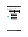
1
!"
#
$
!"
!"!#
!
!!
"
!
$
!
#
%!
!
!!"
"##!#!
!" #!
$!
!
% !
%#"
&
!"
!"
!" AXIOMTEK is a trademark of AXIOMTEK Co., Ltd.
MS-DOS, and Windows !95 are trademarks of Microsoft
Corporation.
AMI is a trademark of American Megatrends Inc.
IBM, PC/AT, PS/2, VGA are trademarks of International Business
Machines Corporation.
Realtek is a trademark of Realtek Semiconductor Corporation.
All brand names and trademarks are the properties and
registered brands of their respective owners.
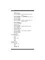
Chapter 1
Introduction
1.2.1
1.2.2
High Speed Multi I/O .............................................................. 3
Environmental and Power ..................................................... 3
1.4.1
Flash Disk DiskOnChip ........................................................... 4
Chapter 2
!"#$% &
'( )
*"($ +
2.3.1
2.3.2
2.3.3
2.3.4
2.3.5
2.3.6
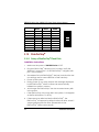
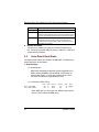
Reset Jumper: JP1 ................................................................... 7
Clear CMOS Setting: JP2........................................................ 7
VGA IRQ9 Operation: JP7...................................................... 7
IRQ3/4/10/11 selection for COM3/COM4: JP9 .................. 8
COM2 RS-232/422/485 Setting: JP10.................................... 8
RS232/422/485 Selection for COM2 Mode: JP11, JP12..... 8
,
Chapter 3
&
)
+
/
,
Installation
Hardware Description
- !(-(! " . ! 3.6.1
3.6.2
3.6.3
3.6.4
Chipset .................................................................................... 13
Display Memory ..................................................................... 13
VGA/Flat Panel Connectors................................................ 14
Flat Panel Connector Pin Description................................ 15
!
&
'' )
' +
3.9.1
Serial Ports IRQ Selection...................................................... 17
Table of Contents
3.9.2
Serial Ports +5V and +12V Power Selection ...................... 17
Table of Contents
0 /
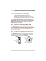
3.10.1 Setup a DiskOnChip Flash Disk .......................................... 18
Installation Instructions ............................................................................................ 18
&
12(-1- ,
3!4'5-" ,
. 0
'50 0
'$( Chapter 4
" " 6" Chapter 5
&
&
&
&
&&
&)
&+
&/
&,
&0
Ethernet
AMI BIOS Setup
-" )
6-" /
6-" 0
'" "7
%
$"6'8 &
"$"8($ )
"$"8$ +
6$.# /
.#9"6$ ,
Appendix A
Watchdog Timer
9$!(2( $"$9
24!8 Chipset Configuration Registers ...................................................... 41
Enable/Disable Watchdog - INDEX 37H ................................................................. 41
Watchdog Time Out Action - INDEX 38H................................................................ 42
Watchdog Timer - INDEX 39H, 3AH, 3BH .............................................................. 42
Timeout Status & Reset - INDEX 3CH .................................................................... 43
Programming the Watchdog .......................................................... 43
Table of Contents
Appendix B
System Assignments
!(5' +
-$( /
"$( /
--(!- ,
Appendix C
POST Error Codes
&
.-$ &
-'2 &
2"4$ &
If the Computer Beeps...................................................................... 53
.-$ &
'2 &)
Uncompressed Code Checkpoints ................................................ 56
Runtime Code is Uncompressed ..................................................... 57
Table of Contents
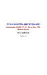
SBC8233 All-in-One 386SX CPU Card Series User's Manual
'('
)#
*
&
/
#$%&'()*+,*-
.+
//
&&
0* 1)))
.
/
&
+*23
+*
Introduction
"
SBC8233 All-in-One 386SX CPU Card Series User's Manual
'(+
*#
#
&
#" Embedded CPU:
#" BIOS:
ALi M6117D is an implementation of an
INTEL compatible 386SX-40 CPU, realtime
clock, a watchdog timer and ALi’s M1217B
chipset
Y2K compliant AMI system BIOS
#" Onboard Memory:
4MB EDO RAM (Bank0)
#" DRAM Memory: 1 x 72-pin SIMM socket (single side type)
supporting up to 16MB EDO RAM
#" Bus Interface:
#" Data Bus:
#" Bus Speed:
16-bit
PC/104 - 8 MHz
(Above values are defaults, bus speeds are
programmable up to 16MHz)
#" DMA Channels:
#" Interrupt Levels:
#" Enhanced IDE:
#" Watchdog Timer:
#" Real-time Clock:
#" Keyboard/Mouse
Connectors:
1
ISA and PC/104
7
15
supports one port and up to two enhanced
IDE (AT Bus) hard drives
generates a RESET, NMI or an IRQ when
your application loses control over the
system. Optionally the watchdog can
trigger a user-specified interrupt. The
watchdog is configurable from 30.5μs to
512 seconds (in 30.5μs segments)
included in M6117D with onboard lithium
battery backup for 10 years of data
retention. CMOS data backup of BIOS
setup and BIOS default.
supports different type connectors of
AT Keyboard and PS/2-mouse
Introduction
SBC8233 All-in-One 386SX CPU Card Series User's Manual
#" Chipset: ALi 5113
#" Serial ports:
#" FDD Interface:
supports high speed RS-232 port, high speed
RS-232/485 port (jumper selectable). Both
with 16C550 UART and 16 byte FIFO
supports up to two floppy drives, 5¼“ (360
KB or 1.2 MB) and 3½“ (720 KB, 1.44 MB)
#" Bi-directional Parallel Port:
supports SPP, EPP and ECP
mode
#" Power Requirements:
Single voltage +5 V
#" Board Dimensions: 185 (L) x 122 (W) mm.
#" Board Weight:
240 g
#" Extended Operating Temperature:
'(
0~+60 °C
,)-#
#" Chipset: TOPRO TP6508IQ
#" Memory: 1 MB onboard
#" System Bus: 16-bit ISA bus
#" Panel Data Bus: 24-bit
#" Display: CRT and Flat Panel Mono/TFT/DSTN/EL
Introduction
#
SBC8233 All-in-One 386SX CPU Card Series User's Manual
'(.
/
*0
/
! !"
#" Package: Single Chip Flash Disk in 32-pin DIP JEDEC
#" Capacity: Up to the most updated capacity
#" Data Reliability: ECC/EDC error correction
#" Memory Window: 8 Kbyte
(
Introduction
SBC8233 All-in-One 386SX CPU Card Series User's Manual
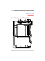
1&2&"0
3
4&
+('
Installation
4
%
44-pin Flat Panel Display PC/104 Bus 40-pin
PC/104 Bus 64-pin
+5V
NC
+12V
-12V
GND
GND
LED1
!
"#
Parallel Port
External CRT Display
Power Connector
FDD Connector
JP11 2JP12
+(+
IDE
SBC8233 All-in-One 386SX CPU Card Series User's Manual
#$
External
PS/2 & AT
K/B
Internal
K/B
CONT7
Installation
SBC8233 All-in-One 386SX CPU Card Series User's Manual
+(
5"$*
4
67/
7
/
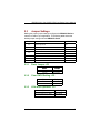
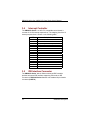
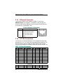
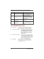
Jumper
Function
Default
JP1
Reset Jumper: Normal
Open
JP2
Clear CMOS Setting: Normal
Open
JP7
VGA IRQ9 Operation: w/o IRQ9
Open
IRQ3/4/10/11 selection for COM3: IRQ10
Short 3-5
IRQ3/4/10/11 selection for COM4: IRQ11
Short 4-6
JP10
RS-232/422/485 selection for COM2: RS-232
Short 1-2
JP11
RS-232/422/485 for COM2 mode: RS-232
Short 3-5, 4-6
JP12
RS-232/422/485 for COM2 mode: RS-232
Short 3-5, 4-6
JP9
#
$%
&%
Options
Reset
Normal
#
Open (default)
""&%
Options
Clear CMOS
Normal
##
Settings
Short 1-2
Settings
Short 1-2
Open (default)
'()$*+
&%,
Options
Installation
Settings
VGA Operation w/o IRQ9
Open (default)
VGA Operation w/ IRQ9
Short
5
SBC8233 All-in-One 386SX CPU Card Series User's Manual
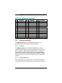
# $*#-./"#"&%+
Mode
IRQ3
IRQ4
IRQ10
IRQ11
COM3
Short 1-3
Open
Short 3-5 (default)
Open
COM4
Open
Short 2-4
Open
Short 4-6 (default)
#0
"$1#20&%-
COM2 Mode
RS-232
RS-422
RS-485
Settings
Short 1-2 (CONT11 active) - default
Short 3-4
Short 5-6
#3 $#20./"&%4
%
Options
RS232
RS-422/485
$
JP11
Short 3-5, 4-6 (default)
Short 1-3, 2-4
JP12
Short 3-5, 4-6 (default)
Short 1-3, 2-4
Installation
SBC8233 All-in-One 386SX CPU Card Series User's Manual
+(.
&#&
**+,
&
/
/
*#
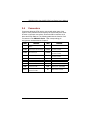
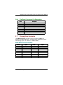
Label
Connector
Label
CON1
External female 15-pin D-type CRT
Display
CONT12
CON2
Internal 44-pin Flat Panel Display
CONT13
CONT2
PC/104 bus 64-pin
CONT14
CONT3
PC/104 bus 40-pin
CONT15
CONT4
CONT6
CONT7
CONT9
External PS/2 and AT keyboard
Power
Internal AT-keyboard
FDD
External 9-pin male D-type
connector for COM1
Internal 10-pin box header
connector for COM2
COM1
CONT11
Installation
Connector
IDE
JP3
JP6
P1
SIM1
Internal 10-pin box header
connector for COM3
Internal 10-pin box header
connector for COM4
Internal 10-pin box header
connector for COM1
Power LED
IDE LED
Parallel Port
Memory bank 0 (EDO DRAM)
SIM2
Memory bank 1 (EDO DRAM)
TP1
Ethernet RJ-45 connector
8
SBC8233 All-in-One 386SX CPU Card Series User's Manual
")
SBC8233 All-in-One 386SX CPU Card Series User's Manual
('
!
#&*&#&
/
69+3:6%""5
&
*+,
,;'0&21 84
6&0&
(+
1-
&0&
/36+
+
0&/./+-06
0&-*
4
360&
(
2$!$&2
/51&66<"=
(6
<)= >
"<"%6=/
1)6
?
14%@4"1@"6(6$6
"%6/0-36
Hardware Description
""
SBC8233 All-in-One 386SX CPU Card Series User's Manual
(.
-"*&&
/"))A+*
"%&3B"%
B
NMI
IRQ0
IRQ1
IRQ2
IRQ3
IRQ4
IRQ5
IRQ6
IRQ7
IRQ8
IRQ9
IRQ10
IRQ11
IRQ12
IRQ13
IRQ14
IRQ15
(6
Parity check error
System timer output
Keyboard
Interrupt rerouting from IRQ8 through IRQ15
Serial port #2
Serial port #1
Parallel port #2
Floppy disk controller
Parallel port #1
Real time clock
Reserved
Serial port #3
Serial port #4
PS/2 Mouse
Math coprocessor
Primary IDE channel
Secondary IDE Channel
-%-#&#&
/:&3
/
/+0
(/
/
()
<;2=
"1
Hardware Description
SBC8233 All-in-One 386SX CPU Card Series User's Manual
CONT12: 40-pin IDE Connector Pin Assignment
Pin
1
4
7
10
13
16
19
22
25
28
31
34
37
40
Description
Reset #
Data 8
Data 5
Data 11
Data 2
Data 14
GND
GND
IOR #
No connector
Interrupt IRQ14
No connector
HDC CS0 #
GND
(
Pin
2
5
8
11
14
17
20
23
26
29
32
35
38
Description
GND
Data 6
Data 10
Data 3
Data 13
Data 0
No connector
IOW #
GND
No connector
IOCS16
SA0
HDC CSI #
Pin
3
6
9
12
15
18
21
24
27
30
33
36
39
Description
Data 7
Data 9
Data 4
Data 12
Data 1
Data 15
No connector
GND
No connector
GND-Default
SA1
SA2
HDD Active #
*2-#
/
CD3
#3
"
/0+-0+%4)$E&CD3
*-
<
CD3=
6CD36
B<=
#3
55
"6CD3
*-
")1(>5%$14%
Hardware Description
"#
SBC8233 All-in-One 386SX CPU Card Series User's Manual
#3#
'()".
/*-CD3
;"4
*-CD3
;
((*
CD3
7
B
CON1: CRT/VGA Connector Pin Assignment
Pin
Signal
Pin
Signal
Pin
Signal
1
Red
2
No connector
Blue
4
Green
No connector
11
3
12
No connector
5
GND
6
GND
13
HSYNC
7
GND
8
GND
14
9
No connector
10
GND
15
VSYNC
No connector
CON2: 44-pin Connector for Flat Panel
Pin
1
4
7
10
13
16
19
22
25
28
31
34
37
40
43
"(
Description
12V
GND
FPVEE
P1
P4
P7
P10
P13
P16
P19
P22
GND
M
ENABKL
VDDM
Pin
2
5
8
11
14
17
20
23
26
29
32
35
38
41
44
Description
12V
VDDM
GND
P2
P5
P8
P11
P14
P17
P20
P23
SCLK
LP
GND
VDDM
Pin
3
6
9
12
15
18
21
24
27
30
33
36
39
42
Description
GND
VDDM
PO
P3
P6
P9
P12
P15
P18
P21
GND
FLM
GND
ASHFCLK
Hardware Description
SBC8233 All-in-One 386SX CPU Card Series User's Manual
#3
". .
Name
Description
P0~P35
ENABKL
SHFCLK
M
LP
FLM
+12VM
Flat panel data output
Activity Indicator and Enable Backlight outputs
Shift clock. Pixel clock for flat panel data
M signal for panel AC drive control
Latch pulse. Flat panel equivalent of HSYNC
First line marker. Flat panel equivalent of VSYNC
+12V power controlled by chipset
ENAVEE
VDDM
Power sequencing controls for panel LCD bias volt
5V
(7
0&**2
/&&
/
#(;2,
#4F51)@"((621$$6
CONT9: FDD Connector Pin Assignment
Pin No.
1-33 (odd)
2
4, 6
8
10
12
14
16
18
Signal
GND
High Density
Unused
Index
Motor Enable A
Driver Select B
Driver Select A
Motor Enable B
Direction
Hardware Description
Pin No.
20
22
24
26
28
30
32
34
Signal
Step Pulse
Write Data
Write Enable
Track 0
Write Protect
Read Data
Select Head
Disk Change
"4
SBC8233 All-in-One 386SX CPU Card Series User's Manual
(
&-#
/
<'=
&++/++/*+
#"Standard mode: IBM PC/XT, PC/AT and PS/2TM compatible
with bi-directional parallel port
#"Enhanced mode: Enhance parallel port (EPP) compatible
with EPP 1.7 and EPP 1.9 (IEEE 1284 compliant)
#"High speed mode: Microsoft and Hewlett Packard extended
capabilities port (ECP) IEEE 1284 compliant
:+"<#5$G=
:+1<15$G=
0&*60&
Pin
"%
Description
Pin
Description
1
Strobe
2
Data 0
3
Data 1
4
Data 2
5
Data 3
6
Data 4
7
Data 5
8
Data 6
9
Data 7
10
Acknowledge #
11
Busy
12
Paper Empty #
13
Printer Select
14
Auto Form Feed #
15
Error #
16
Initialize #
17
Printer Select In #
18
GND
19
GND
20
GND
21
GND
22
GND
23
GND
24
25
GND
26
GND
No connector
Hardware Description
SBC8233 All-in-One 386SX CPU Card Series User's Manual
(8
&-#
/
-<;2&=
-<;2=
-<;2=-&1#1
-
<;2=-&1#12(112($473
H4C2"1C"
$
7
#+
$*.
/
-
-
--&1#1
--&1#12(112($4
73H4C2"1C
"
$8
7
#+
60'6'.
*06H4C2H"1C"
$
7-&1#1
CONT11/13/14/15: COM2/3/4/1 Serial Port Connectors Pin Assignment
Pin
1
3
5
7
9
Description
Data Carrier Detect (DCD)
Receive Data (RXD)
Transmit Data (TXD)
Data Terminal Ready (DTR)
Ground (GND)
Pin
2
4
6
8
10
Description
Data Set Ready (DSR)
Request to Send (RTS)
Clear to Send (CTS)
Ring Indicator (RI)
Ground (GND)
-&(112($4;2<*061=
Hardware Description
"5
SBC8233 All-in-One 386SX CPU Card Series User's Manual
CONT11 Pin
1
2
3
4
5
6
7
8
9
10
RS-232
DCD
DSR
RX
RTS
TX
CTS
DTR
RI
GND
GND
RS-422
TXNo connector
TX+
No connector
RX+
No connector
RXNo connector
GND
GND
RS-485
DATANo connector
DATA+
No connector
No connector
No connector
No connector
No connector
GND
GND
('9 /
*
#- !"
!
Installation Instructions
1.
Make sure the power of SBC8233 Series is OFF.
2.
Plug the DiskOnChip device(s) into its socket. Verify the
direction is correct (pin 1 of the DiskOnChip is aligned with
pin 1 of the socket)
3.
Set address for both DiskOnChip devices (note that the last
two settings are for normal EPROM or Flash devices)
4.
Power up the system
5.
During power up you may observe the messages displayed
by the DiskOnChip when its drivers are automatically
loaded into system’s memory
6.
At this stage the DiskOnChip can be accessed as any disk
in the system
7.
If the DiskOnChip is the only disk in the system, it will appear
as the first disk (drive C: in DOS)
8.
If there are more disks besides the DiskOnChip, the
DiskOnChip will appear by default as the last drive, unless it
was programmed as first drive. (Please refer to the
DiskOnChip utilities user manual).
"$
Hardware Description
SBC8233 All-in-One 386SX CPU Card Series User's Manual
9.
If you want the DiskOnChip to be bootable:
a. Copy the operating system files into the DiskOnChip by using
the standard DOS command (for example: sys d:).
b. The DiskOnChip should be the only disk in the systems or
should be configured as the first disk in the system (c: ) using
the DUPDATE utility.
.0*6&
>55
,6
&
3;
0*&2 ,
('' $&#/!!
/6%""5-*<-*=
*60&-36
&/,+3")
-*
*60&-36
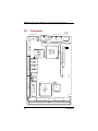
('+ :2;&+!&"&#&
/
>3
+&21
;<;2=
3
4<;2+=
CONT7
Hardware Description
CONT4
"8
SBC8233 All-in-One 386SX CPU Card Series User's Manual
(' %&#&
-I(4
-I(42'
/")"))7
2'
<7=
")2"))
TP1: RJ-45 Connector Pin Assignment
Pin
1
2
3
6
other
Signal
Tx+ (Data transmission positive)
Tx- (Data transmission negative)
Rx+(Data reception positive)
Rx- (Data reception negative)
Not use
('. '9.&#&
+*2")(
#%J>#$J
&3
+*2")(
+*2")(
>
20
K
CONT2: PC/104 Bus Pin Assignment
Pin#
1
5
9
13
17
21
25
29
33
37
Pin#
41
1)
Pin Name
IOCHCHK*
SD6
SD4
SD2
SD0
AEN
SA18
SA16
SA14
SA12
Pin#
Pin Name
SA10
Pin#
2
6
10
14
18
22
26
30
34
38
42
Pin Name
GND
+5V
-5V
-12V
+12V
SMEMW*
IOW*
DACK3*
DACK1*
REFRESH*
Pin#
3
7
11
15
19
23
27
31
35
39
Pin Name Pin# Pin Name
SD7
RESETDRV
4
SD5
IRQ9
8
SD3
12 DRQ2
SD1
16 ENDXFR*
IOCHRDY 20 GND
SA19
24 SMEMR*
SA17
28 IOR *
SA15
32 DRQ3
SA13
36 DRQ1
SA11
40 SYSCLK
Continued . . . . .
Pin Name
Pin# Pin Name Pin# Pin Name
IRQ7
SA9
43
44 IRQ6
Hardware Description
SBC8233 All-in-One 386SX CPU Card Series User's Manual
45
49
53
57
61
SA8
SA6
SA4
SA2
SA0
46
50
54
58
62
IRQ5
IRQ3
TC
+5V
GND
47
51
55
59
63
SA7
SA5
SA3
SA1
GND
48
Pin Name
Pin#
52
56
60
64
IRQ4
DACK2*
SALE
OSC
GND
CONT3: PC/104 Bus Pin Assignments
Pin#
1
5
9
13
17
21
25
29
33
37
Pin Name
GND
IOCS16*
IRQ11
IRQ15
DACK0*
DACK5*
DACK6*
DACK7*
+5V
GND
Pin#
2
6
10
14
18
22
26
30
34
38
Hardware Description
Pin Name
GND
LA23
LA21
LA19
LA17
MEMW*
SD9
SD11
SD13
SD15
Pin#
3
7
11
15
19
23
27
31
35
39
MEMCS16*
IRQ10
IRQ12
IRQ14
DRQ0
DRQ5
DRQ6
DRQ7
MASTER*
GND
4
8
12
16
20
24
28
32
36
40
Pin Name
SBHE*
LA22
LA20
LA18
MEMR*
SD8
SD10
SD12
SD14
(KEY)
1"
SBC8233 All-in-One 386SX CPU Card Series User's Manual
('6 4$&&#&
CONT6: Power Connector
Pin
1
2
3
Description
No connector
+5V
+12V
Pin
Pin
Description
4
5
6
Description
-12V
GND
GND
JP3: Power LED
1
2
3
Vcc
No connector
Ground
JP6: IDE LED
Pin
1
2
11
Description
Vcc
Signal
Hardware Description
SBC8233 All-in-One 386SX CPU Card Series User's Manual
.('
-&"#
&
/B
+
+////$)1#
-I(4
-:$)"83&-:$)"8
"%@&-36
&-36
.(+
0"
#" RTL8019 software compatible
#" Supports PnP auto detect mode
#" 16k byte SRAM built in
#" Supports flash memory read/write
#" Supports UTP and auto-detect
#" Supports IO address fully decode mode
#" Makes PnP jumper option more user-friendly
#" Improves the blinking problem of CRS LED when the cable is
not connected
Ethernet
1#
SBC8233 All-in-One 386SX CPU Card Series User's Manual
.( <"**&
//
>7
;; 1>#>6:3;
6 #" 846:3;&&*0,;'0
;&
+
1(
Ethernet
SBC8233 All-in-One 386SX CPU Card Series User's Manual
!"#
0&
?
<
C
*
=
+0&<+0&
=3
I
&/,+
+L/:M<*-:3:/:=
360&N>
*60&
L;&M
*60&
!
6
? AMI BIOS Setup
14
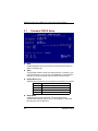
SBC8233 All-in-One 386SX CPU Card Series User's Manual
6('
!"*
#" Date
The BIOS determines the day of the week from the other date information; this
field is for information only.
#" Time
The time format is based on the 24-hour military-time clock. For example, 1 p.m.
is 13:00:00. Press the « or ( key to move to the desired field . Press the PgUp or
PgDn key to increment the setting, or type the desired value into the field.
#" Floppy Drive A, B
Select the correct specifications for the diskette drive(s) installed in the computer.
None
360K
1.2M
720K
1.44M
No diskette drive installed
5.25 in5-1/4 inch PC-type standard drive
5.25 in5-1/4 inch AT-type high-density drive
3.5 in3-1/2 inch double-sided drive
3.5 in3-1/2 inch double-sided drive
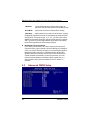
#" Hard Disks
The BIOS supports up to four IDE drives. This section does not show
information about other IDE devices, such as a CD-ROM drive, or about other
hard drive types, such as SCSI drives.
1%
AMI BIOS Setup
SBC8233 All-in-One 386SX CPU Card Series User's Manual
NOTE:
It is recommended that you select type AUTO for all drives.
The BIOS can automatically detect the specifications and optimal operating
mode of almost all IDE hard drives. When you select type AUTO for a hard drive,
the BIOS detects its specifications during POST, every time the system boots. If
you do not want to select drive type AUTO, other methods of selecting the drive
type are available:
1.
Match the specifications of your installed IDE hard drive(s) with
the preprogrammed values for drive types 1 through 45.
2.
Select USER and enter values into each drive parameter field.
3.
Use the IDE HDD AUTO DETECTION function in Setup.
Here is a brief explanation of drive specifications:
&
!"
'(&
#$
%&'
#
#(#
!&
'
) &
'
*$+,&
)*
+ ,
#
#
#
#
-
#
)*
#
.
.
#
+ $-!
..
&
'+&
'
AMI BIOS Setup
15
SBC8233 All-in-One 386SX CPU Card Series User's Manual
-
/
#-0
1230$4&
-+.
#0
$4&
/-
52($4&
PIO Mode IDE Programmed I/O mode. PIO programming also works with ATAPI
CD-ROM drives. The settings are Auto, 0, 1, 2, 3, 4, or 5. Click on Auto to allow
AMIBIOS to automatically find the PIO mode that the IDE drive being configured
uses. If you select 0-5 you must make absolutely certain that you are selecting
the PIO mode supported by the IDE drive being configured.
#" BootSector Virus Protection
It is not exactly a virus protection. All it does is whenever your boot sector is
accessed for writing, it gives a warning to the screen allowing you to disable the
access or to continue. Extremely annoying if you use something like OS/2 Boot
Manager that needs to write to it. It is completely useless for SCSI or ESDI
(Enhanced Small Device Interface) drives as they use their own BIOS on the
controller. Disabled recommended. If you want virus protection, use a TSR
(Terminate and Stay Resident) virus detection (Norton, Central Point, etc...).
Scan by McAfee is also a good idea. Available on most FTP servers, it is
shareware.
6(+
<#!"*
1$
AMI BIOS Setup
SBC8233 All-in-One 386SX CPU Card Series User's Manual
#" 1st Boot Device
Specifies the first device for which to look and use for booting the system.
Options are : Disabled 1st IDE-HDD, 2nd IDE-HDD, 3rd IDE-HDD, 4th IDE-HDD,
Floppy, ARMD-FDD, ARMD-HDD, ATAPI CDROM, SCSI or NETWORK.
ARMD (FDD/HDD) means “ATAPI Removable Media Device”.
#" 2nd Boot Device
Specifies the second device for which to look and use for booting the system.
Options are : Disabled 1st IDE-HDD, 2nd IDE-HDD, 3rd IDE-HDD, 4th IDE-HDD,
Floppy, ARMD-FDD, ARMD-HDD, ATAPI CDROM, SCSI or NETWORK.
#" Floppy Drive Swap
This field is effective only in systems with two floppy drives. Selecting Enabled
assigns physical drive B to logical drive A, and physical drive A to logical drive B.
#" PS/2 Mouse Support
This setting is specially for those users who whish to connect a PS/2 mouse.
Enabling reserves IRQ 12 for the PS/2 mouse. Disabling releases the IRQ 12 for
use by another system component.
#" System Keyboard
“Present”. If “Absent” is selected this option sets the BIOS to pass the keyboard
test in the POST, allowing to reset a PC without a keyboard (file server, printer
server, etc.), without the BIOS producing a keyboard error.
#" Primary display
The type of display standard you are using. The most frequent is VGA/PGA/EGA.
Modern computers have VGA (Video Graphics Array). If you have an older
black/ white display select Mono. If you want to use the board without display
controller set this value to “Absent”. This option sets the BIOS to pass the
display controller test in the POST, allowing to boot a PC without a display
controller. Even if set to “Absent” the board will still try to initialize a display card
if present.
#" Password Check
If you have set a password, select whether the password is required every time
the System boots, or only when you enter the BIOS Setup.
Always
Setup
AMI BIOS Setup
The system will not boot and access to Setup will be denied if the
correct password is not entered at the prompt.
The system will boot, but access to Setup will be denied if the correct
password is not entered at the prompt.
18
SBC8233 All-in-One 386SX CPU Card Series User's Manual
#" C8000, 16 K Shadow
Specifies whether the specified area of ROM is to be shadowed and if shadowed,
whether it should be written to or read from cache memory. The fail-safe default
is Disabled.
CAUTION:
Some option ROMs do not operate properly
when shadowed.
!"CC000, 16 K Shadow
!"D0000, 16 K Shadow
!"D4000, 16 K Shadow
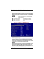
6(
!"D8000, 16 K Shadow
!"DC000, 16 K Shadow
!"
<#
*!"*
#" VGA Frame Buffer Size
The STPC implements a single memory subsystem for both the system as well
as the frame buffer memory. In other words, the size of the DRAM available to
the system is reduced by the size of the DRAM allocated to the frame buffer.
The lower range of the DRAM, starting from the DRAM address 00h, is allocated
to frame buffer. The rest of the memory is used by the system.
#" ISACLK
Set the speed of the ISA bus here. The settings are tied to the speed of the PCI
bus. If the PCI bus operates at 33 MHz, a setting of PCICLK/4 (default) would
yield an ISA bus speed of approximately 8 MHz, the standard speed of the ISA
bus. While most devices operate at higher ISA bus speeds, try a slower bus
speed if your ISA device does not function properly.
#)
AMI BIOS Setup
SBC8233 All-in-One 386SX CPU Card Series User's Manual
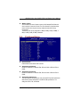
#" Memory Hole
You can reserve this area of system memory for ISA adapter ROM. When this
area is reserved, it cannot be cached. The user information of peripherals that
need to use this area of system memory usually discusses their memory
requirements.
The memory hole can be configured as 1 MB (15-14MB), 2 MB (15-13MB), 4
MB (15-11MB), 8 MB (15-7MB) or disabled.
6(.
*"*
#" Onboard FDC
Enable/disable or Auto detect FDD Controller
#" Onboard Serial Port1
Disable or enable wtih I/O address 3E8h, 3F8h as COM1 or 2E8h or 2F8h as
COM2
#" Onboard Serial Port1
Disable or enable wtih I/O address 3E8h, 3F8h as COM1 or 2E8h or 2F8h as
COM2
#" Onboard Parallel Port
This option specifies the parallel port mode. ECP and EPP are both bidirectional
data transfer schemes that adhere to the IEEE P1284 specifications. The
settings are 378h, 278h, or Disabled.
AMI BIOS Setup
#"
SBC8233 All-in-One 386SX CPU Card Series User's Manual
Normal
Bi-Dir
The normal parallel port mode is used.
Supports bidirectional transfers on the parallel port.
EPP
The parallel port can be used with devices that adhere to the Enhanced
Parallel Port (EPP) specification. EPP uses the existing parallel port signals
to provide asymmetric bidirectional data transfer driven by the host device.
ECP
The parallel port can be used with devices that adhere to the Extended
Capabilities Port (ECP) specification. ECP uses the DMA protocol to
achieve transfer rates of approximately 2.5 Mbs. ECP provides symmetric
bidirectional communications.
#" Parallel Port DMA
This option is only available if the setting for the Parallel Port Mode option is
ECP. The settings are Disabled, DMA CH (channel) 0, DMA CH 1, or DMA CH 3.
The default setting is Disabled.
6(6
"&#
/
//
360&
"$
LM3
0&
G
;0-63::39:3-D/G
:3
!:3!,
LM&
*60&&
"#$%&'()
"#$"%'
()
,
,
! *+
, ----------
GO!J60/J
G
#1
AMI BIOS Setup
SBC8233 All-in-One 386SX CPU Card Series User's Manual
%
-
3
0&#G
;0-63::39
:3-D/
!";1- (
3
0&/
>
9
;0-63:
")1("%9%#
no. Cylinder
x no. Head
x no. Sector
x no. per sector
(
(
(
(
1024)
16)
63)
512)
528 Megabytes
G;0-63:
>
G?41$6
?P
!"LBA (Logical Block Addressing) mode
3G
41$6
9
G
G/
9
G
>G?
:3
$(D
no. Cylinder
x no. Head
x no. Sector
x bytes per sector
AMI BIOS Setup
(
(
(
(
1024)
255)
63)
512)
814 Gigabytes
##
SBC8233 All-in-One 386SX CPU Card Series User's Manual
!" 1.(
/>
G
3
&
&/G")1(
:3
<
:3=3
0&
GP
/>:3-D/
CYLS
1120
560
HEADS
16
32
SECTOR
59
59
MODE
NORMAL
LARGE
0&0&<0&=
")1(
13
13
;"#
G
P
6>G?
no. Cylinder
x no. Head
x no. Sector
x bytes per sector
#(
(
(
(
(
1024)
32)
63)
512)
1 Gigabytes
AMI BIOS Setup
SBC8233 All-in-One 386SX CPU Card Series User's Manual
6(
4"*<
&&
ENTER PASSWORD:
L/M
*60&N
L/MNL/M
7L/M
3
0
&
PASSWORD DISABLED.
&&00&.&6
&&
&00&.&6
&
AMI BIOS Setup
#4
SBC8233 All-in-One 386SX CPU Card Series User's Manual
6(7
"&&
4"
&
*
$
4
#%
AMI BIOS Setup
SBC8233 All-in-One 386SX CPU Card Series User's Manual
6(
"&&
4"
&
0
4
0&-06
AMI BIOS Setup
#5
SBC8233 All-in-One 386SX CPU Card Series User's Manual
6(8
<
4%3
QNJB
*60&Q;J
&
#$
AMI BIOS Setup
SBC8233 All-in-One 386SX CPU Card Series User's Manual
6('9 %3
=
&"<
4
&>&
QNJB&
Q;J&
AMI BIOS Setup
#8
SBC8233 All-in-One 386SX CPU Card Series User's Manual
()
SBC8233 All-in-One 386SX CPU Card Series User's Manual
!$!
%&'
#15%$@G?B1(
#)44"1
#)4 &-/&/
;6-E
1(
%$
-/&/
;6-E
=#&4&2$
$
3
-E,
0&$14()-E)
4(8
)
-E
-E
&
4"
4=;2&
"
"/$
6%""5;/'#5G#$G#8G#3G#G
#*G
2
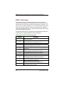
Enable/Disable Watchdog - INDEX 37H
Bit
7
6
5-0
Value
reserved
0
1
Other function
Watchdog Timer
Action
Do not modify the value of these bits!
Disable watchdog timer
Enable watchdog timer
Do not modify the value of these bits!
("
SBC8233 All-in-One 386SX CPU Card Series User's Manual
Watchdog Time Out Action - INDEX 38H
Bit
Value
7-4
3-0
Action
0000
0001
0010
0011
0100
0101
0110
0111
1000
1001
1010
1011
1100
1101
1110
1111
Other function
No output signal
IRQ3
IRQ4
IRQ5
IRQ6
IRQ7
IRQ9
IRQ10
IRQ11
IRQ12
IRQ14
IRQ15
NMI
System RESET
No output signal
No output signal
Do not modify the value of these bits!
Watchdog Timer - INDEX 39H, 3AH, 3BH
Index
Bits
counter
3BH
3AH
D7……D0
[VSB…………….
39H
D7……D0
…………………...
D7……D0
………..LSB]
For example
Index
3Bh
00h
00h
00h
00h
01h
02h
FFh
(1
3AH
00h
00h
01h
02h
00h
00h
FFh
39H
01h
02h
00h
00h
00h
00h
FFh
Time out
30.56s
616s
7.8 ms
15.6 ms
2s
4s
512 s
Watchdog Timer
SBC8233 All-in-One 386SX CPU Card Series User's Manual
Timeout Status & Reset - INDEX 3CH
Bit
Value
Action
7
0
1
Timeout has not occurred
Timeout has ocurred
1
0
Reset timer
Has no meaning
6
5
4-0
Other function, do not modify these bits
7.
07889 #
#
0!+.
+!1" !
+.
+!1" !
mov
out
nop
nop
mov
out
nop
nop
mov
out
nop
nop
mov
out
nop
nop
al, 013h
22h, al
al, 0c5h
23h, al
al, 013h
22h, al
al, 000h
23h, al
Read the value of a configuration register
.>
;/'#*G
0!+.
+!1" !
mov al, 03ch
out 22h, al
nop
nop
in al, 23h
nop
nop
push ax
+.
+!1" !
pop ax ;AL - result
Watchdog Timer
(#
SBC8233 All-in-One 386SX CPU Card Series User's Manual
Write data to configuration register
.>)..;/'#
0!+.
+!1" !
mov
out
nop
nop
mov
out
nop
nop
al, 03bh
22h, al
al, 0ffh
23h, al
+.
+!1" !
Watchdog Program Example
B?
Step 1.
Unlock configuration register.
Step 2.
Disable watchdog timer by setting INDEX 37H Bit 6 to ‘0’.
Step 3.
Set the expected counter value to INDEX 3BH, 3AH, 39H.
Step 4.
Select timeout action from INDEX 38H Bit 7-4.
Step 5.
Enable watchdog timer by setting INDEX 37H Bit 6 to ‘1’.
Step 6.
Lock configuration register.
/>&"1$-/&/
; Please use MASM to compiler the following program
; Execute under DOS environment
dosseg
. model small
. stack 100h
.code
main proc
mov ax, 0c513h ; Unlock config. register
call writechip
mov ax, 03737h ; Disable watchdog timer
call readchip
and al, 10111111b
((
Watchdog Timer
SBC8233 All-in-One 386SX CPU Card Series User's Manual
xchg ah, al
call writechip
mov ax, 0403bh ; Set the expected counter
; value
call writechip ; to [400000h]
mov ax, 0003ah ; 30.5*sec*400000h= 128 sec
call writechip
mov ax, 00039h
call writechip
mov ax, 03838h ; Select “system reset” as
; timeout action
call readchip
and al, 00001111b
or al, 11010000b
xchg ah, al
call writechip
mov ax, 03737h ; Enable watchdog timer
call readchip
or al, 01000000b
xchg ah, al
call writechip
mov ax, 00013h ; Lock config. register
call writechip
mov ax, 04c00h
int 21h
main endp
readchip proc
out 22h, al
nop
nop
in al, 23h
nop
nop
ret
readchip endp
writechip proc
out 22h, al
nop
nop
xchg ah, al
out 23h, al
Watchdog Timer
(4
SBC8233 All-in-One 386SX CPU Card Series User's Manual
nop
nop
xchg ah, al
ret
writechip endp
end main
Reset watchdog timer
-
mov ax, 0c513h ; Unlock configuration
; register
call writechip
mov ax, 03C3Ch ; Reset watchdog timer
; counter
call readchip
or al, 00100000b ; The counter is reset at
xchg ah, al ; out 23h, al
call writechip
mov ax, 00013h ; Lock configuration
; register
call writechip
(%
Watchdog Timer
SBC8233 All-in-One 386SX CPU Card Series User's Manual
!$
('!&'
2$-&
>$%*+,20"@
20>
Address
000-01F
020-03F
040-05F
060-06F
070-07F
080-09F
0A0-0BF
0C0-0DF
0F0
0F1
0F8-0FF
10C-10E
120-123
1F0-1F8
200-207
300-31F
360-36F
378-37F
3F0-3F7
3F8-3FF
2F8-2FF
370
System Assignments
Devices
DMA controller #1
Interrupt controller #1
Timer
Keyboard controller
Real time clock, NMI
DMA page register
Interrupt controller #2
DMA controller #2
Clear math co-processor busy signal
Reset math co-processor
Math processor
RAM/ROM disk program port address
Watch-dog timer operation
Fixed disk controller
Game port
Prototype card
Reserved
Parallel port #1
Floppy disk controller
Serial port #1(COM1)
Serial port #2(COM2)
Onboard I/O (SMC37C669) Configuration Register
(5
SBC8233 All-in-One 386SX CPU Card Series User's Manual
!
4$
Channel
0
1
2
3
4
5
6
7
Function
-
-
:
#$3(&
-
.
0-
8
-
-
-
-"*
4$
/+*
"%&3B
("%
&3+*"%B
R
NMI
IRQ0
IRQ1
IRQ2
IRQ3
IRQ4
IRQ5
IRQ6
IRQ7
IRQ8
IRQ9
IRQ10
IRQ11
IRQ12
IRQ13
IRQ14
IRQ15
($
Parity check error
System timer output
Keyboard
Interrupt rerouting from IRQ8 through IRQ15
Serial port #2
Serial port #1
Selectable for Parallel port
Floppy disk controller
Parallel port #1
Real time clock
Reserved
Reserved
Reserved
PS/2 mouse
Math co-processor
Primary IDE channel
Reserved
System Assignments
SBC8233 All-in-One 386SX CPU Card Series User's Manual
'!1!$&2!*
Address
Size Description
00000000h-0009FFFFh
000A0000h-000BFFFFh
000C0000h-000C3FFFh
!"#$
000C4000h-000C7FFFh
!"#$
000C8000h-000CBFFFh
$%
000CC000h-000CFFFFh
$%
000D0000h-000DFFFFh
$%
System Assignments
(8
SBC8233 All-in-One 386SX CPU Card Series User's Manual
4)
SBC8233 All-in-One 386SX CPU Card Series User's Manual
!$
)#
1*&
.
360&+0&?
1*%&!4
Beeps
1
2
3
4
5
6
7
Error Message
Description
The memory refresh circuitry of the board
DRAM Refresh Failure
is faulty.
A parity error was detected in the base
Parity Circuit Failure
memory (first 64k Block) of the system.
Base 64 KB Memory Failure
A memory failure occurred within the first
64k of memory.
Timer #1 on the system board has failed
System Timer Failure
to function properly.
The CPU on the system board has
Processor Error
generated an error.
Keyboard Controller 8042-Gate
The keyboard controller (8042) contains
A20 error
the gate A20 switch that allows the
computer to operate in virtual mode. This
error message means that the BIOS is not
able to switch the CPU into protected
mode.
Virtual Mode (processor) Exception The CPU on the motherboard has
error
generated an Interrupt Failure exception
interrupt.
Continued . . . . .
POST Error Codes
4"
SBC8233 All-in-One 386SX CPU Card Series User's Manual
Beeps
8
Error Message
Description
Display Memory R/W Test Failure
The system video adapter is either
missing or Read/Write Error its memory is
faulty. This is not a fatal error.
The ROM checksum value does not
match the value encoded in the BIOS.
This is good indication that the BIOS
ROMs went bad.
The shutdown register for CMOS RAM
has failed.
The cache memory test failed. Cache
memory is disabled. Do not press <Ctrl>
<Alt> <Shift> <+> to enable cache
memory.
9
ROM-BIOS Checksum Failure
10
CMOS Shutdown Register
Read/Write Error
11
Cache Memory Bad — Do Not
Enable Cache
!-1-&
#" 2 short beeps
POST failed. This is caused by a failure of
one of the hardware testing procedures.
#" 1 long & 2 short beeps
Video failure. This is caused by one
of two possible hardware faults. 1)
Video BIOS ROM failure, checksum
error encountered. 2) The video
adapter installed has a horizontal
retrace failure.
#" 1 long & 3 short beeps
Video failure. This is caused by one
of three possible hardware problems.
1) The video DAC has failed. 2) the
monitor detection process has failed.
3) The video RAM has failed.
#" 1 long beep
41
POST successful. This indicates that all
hardware tests were completed without
encountering errors.
POST Error Codes
SBC8233 All-in-One 386SX CPU Card Series User's Manual
&";&&
4
/"
8
If it beeps...
1, 2, or 3 times...
No beeps, No boot
6 times...
8 times...
9 times...
11 times...
4, 5, 6, 7, or 10
times...
POST Error Codes
then...
re-install the memory SIMMs or DIPs. If the system still
beeps, replace the memory.
If no beeps are heard and no display is on the screen, The first
thing to check is the power supply. Connect a LED to the POWER
LED connection on the motherboard. If this LED lights and the
drive(s) spin up then the power supply will usually be good.
Next, inspect the motherboard for loose components. A loose or
missing CPU, BIOS chip, Crystal Oscillator, or Chipset chip will
cause the motherboard not to function. Next, eliminate the
possibility of interference by a bad or improperly set up I/O card
by removing all card except the video adapter. The system should
at least power up and wait for a drive time-out. Insert the cards
back into the system one at a time until the problem happens
again. When the system does nothing, the problem will be with
the last expansion card that was put in. If the above suggestions
fail to cause any change in the malfunction of the system, the
motherboard must be returned for repair.
re-install the keyboard controller chip. If it still beeps,
replace the keyboard controller. If it still beeps, try a
different keyboard, or replace the keyboard fuse (if the
keyboard has one).
there is a memory error on the video adapter. Replace the
video adapter, or the RAM on the video adapter.
the BIOS ROM chip is bad. The system probably needs a
new BIOS ROM chip.
re-install the cache memory on the motherboard. If it still
beeps, replace the cache memory.
the motherboard must be repaired or replaced.
4#
SBC8233 All-in-One 386SX CPU Card Series User's Manual
#%&!4
#" 8042 Gate A20 Error
Gate A20 on the keyboard controller (8042) is not working.
#" Address Line Short!
Error in the address decoding circuitry.
#" Cache Memory Bad, Do Not Enable Cache!
Cache memory is defective.
#" CH2 Timer Error
There is an error in timer 2. Several systems have two timers.
#" CMOS Battery State Low
The battery power is getting low. It would be a good idea to replace the battery.
#" CMOS Checksum Failure
After CMOS RAM values are saved, a checksum value is generated for error
checking. The previous value is different from the current value.
#" CMOS System Options Not Set
The values stored in CMOS RAM are either corrupt or nonexistent.
#" CMOS Display Type Mismatch
The video type in CMOS RAM is not the one detected by the BIOS.
#" CMOS Memory Size Mismatch :
The physical amount of memory on the motherboard is different than the amount
in CMOS RAM.
#" CMOS Time and Date Not Set :
Self evident.
#" Diskette Boot Failure
The boot disk in floppy drive A: is corrupt (virus?). Is an operating system
present?
#" Display Switch Not Proper
A video switch on the motherboard must be set to either color or monochrome.
#" DMA Error
Error in the DMA controller.
#" DMA number 1 Error
Error in the first DMA channel.
4(
POST Error Codes
SBC8233 All-in-One 386SX CPU Card Series User's Manual
#" DMA number 2 Error
Error in the second DMA channel.
#" FDD Controller Failure
The BIOS cannot communicate with the floppy disk drive controller.
#" HDD Controller Failure
The BIOS cannot communicate with the hard disk drive controller.
#" INTR number 1 Error
Interrupt channel 1 failed POST.
#" INTR number 2 Error
Interrupt channel 2 failed POST.
#" Keyboard Error
There is a timing problem with the keyboard.
#" KB/Interface Error
There is an error in the keyboard connector.
#" Parity Error ????
Parity error is in system memory at an unknown address.
#" Memory Parity Error at xxxxx
Memory failed at the xxxxx address.
#" I/O Card Parity Error at xxxxx
An expansion card failed at the xxxxx address.
#" DMA Bus Timeout
A device has used the bus signal for more than allocated time (around 8
microseconds).
POST Error Codes
44
SBC8233 All-in-One 386SX CPU Card Series User's Manual
&
/ *
%*.
*.
,$,
&
,
20$)
36
0&
>
9.
"".!
Checkpoint
C2
C5
C6
C7
C8
CA
CB
CD
CE
CF
D1
D2
4%
Description
NMI is Disabled.
Power on delay starting.
Power-on delay complete.
Going to enable ROM. (i.e., disable Cache if any)
Calculating ROM BIOS checksum.
ROM BIOS checksum passed.
CMOS shutdown register test to be done next.
CMOS shutdown register test done. CMOS checksum calculation to
be done next.
CMOS checksum calculation is done, CMOS Diag byte written.
CMOS status register about to init for date and time.
CMOS status register init done.
Any initialization before keyboard BAT to be done next.
BAT command to keyboard controller is to be issued.
Keyboard controller BAT result verified.
Any initialization after KB controller BAT to be done next.
Initialization after KB controller BAT done.
Keyboard command byte to be written next.
Keyboard controller command byte is written.
Going to check pressing of <INS> key during power-on.
Checking for pressing of <INS> key during power-on done. Going to
disable DMA and Interrupt controllers.
POST Error Codes
SBC8233 All-in-One 386SX CPU Card Series User's Manual
$"9.
Checkpoint
D3
D4
D5
DD
01
02
03
05
06
08
09
0A
0B
0C
0D
0E
0F
10
11
Description
DMA controller #1, #2, interrupt controller #1, #2 disabled. Video
display is disabled and port-B is initialized.
Chipset initialization/ auto memory detection over.
To uncompress the RUNTIME code.
RUNTIME code is uncompressed.
Transfer control to uncompressed code in shadow ram at F000:FFF0.
Processor’s register test about to start, and NMI to be disabled.
NMI is Disabled.
Power on delay starting.
Power on delay complete.
To check soft reset/power-on.
Soft reset/power-on determined.
Going to disable Cache if any.
POST code to be uncompressed.
POST code is uncompressed.
CMOS checksum calculation to be done next.
CMOS checksum calculation is done, CMOS Diag byte written.
CMOS init to begin (If "INIT CMOS IN EVERY BOOT IS SET").
CMOS initialization done (if any).
CMOS status register about to init for Date and Time.
CMOS status register init done.
Any initialization before keyboard BAT to be done next.
KB controller I/B free.
Going to issue the BAT command to keyboard controller.
BAT command to keyboard controller is issued.
Going to verify the BAT command.
Keyboard controller BAT result verified.
Any initialization after KB controller BAT to be done next.
Initialization after KB controller BAT done.
Keyboard command byte to be written next.
Keyboard controller command byte is written.
Going to issue Pin-23, 24 blocking/unblocking command.
Pin-23, 24 of keyboard controller is blocked/unblocked.
Going to check pressing of <INS> key during power-on.
Continued . . . . .
POST Error Codes
45
SBC8233 All-in-One 386SX CPU Card Series User's Manual
Checkpoint
12
13
14
19
1A
20
23
24
25
26
27
28
2A
2B
2C
2D
2E
Description
Checking for pressing of <INS> key during power-on done. Going to
disable DMA and interrupt controllers.
DMA controller #1, #2, interrupt controller #1, #2 disabled. Video
display is disabled and port-B is initialized. Chipset init about to
begin.
Chipset initialization over.
8254 timer test about to start.
8254 timer test over.
About to start memory refresh test.
Memory Refresh line is toggling.
Going to check 15 micro second ON/OFF time.
Memory Refresh period 30 micro second test complete.
Base 64K test about to start.
Base 64K test passed.
Going to set BIOS stack and to do any setup before Interrupt vector
init.
Setup required before vector initialization complete.
Interrupt vector initialization about to begin.
Interrupt Vector initialization done.
Going to read input port of 9042 for turbo switch (if any) and to clear
password if post diag switch is on.
Input port of 8042 is read.
Going to initialize global data for turbo switch.
Global data initialization for turbo switch is over.
Any initialization before setting Video mode to be done next.
Initialization before setting Video mode is complete.
Going for monochrome mode and color mode setting.
Different BUSes init (system, static, output devices) to start if present.
(Please see Reference for details of different BUSes)
About to give control for any setup required before optional Video
ROM check.
Processing before Video ROM control is done.
About to look for optional Video ROM and give control.
Optional Video ROM control is done. About to give control to do any
processing after Video ROM returns control.
Return from processing after the Video ROM control.
If EGA/VGA not found then do display memory R/W test.
Continued . . . . .
4$
POST Error Codes
SBC8233 All-in-One 386SX CPU Card Series User's Manual
Checkpoint
2F
30
Description
EGA/VGA not found.
Display memory R/W test about to begin.
Display memory R/W test passed.
About to look for the retrace checking.
31
Display memory R/W test or retrace checking failed.
About to do alternate Display memory R/W test.
32
Alternate Display memory R/W test passed.
About to look for the alternate display retrace checking.
34
Video display checking over.
Display mode to be set next.
37
Display mode set.
Going to display the power on message.
38
Different BUSes init (input, IPL, general devices) to start if present. (Please
see Reference for details of different BUSes)
39
Display different BUSes initialization error messages. (Please see Reference
for details of different BUSes)
3A
New cursor position read and saved.
Going to display the Hit <DEL> message.
3B
Hit <DEL> message displayed.
Virtual mode memory test about to start.
40
Going to prepare the descriptor tables.
42
Descriptor tables prepared.
Going to enter in virtual mode for memory test.
43
Entered in the Virtual mode.
Going to enable interrupts for diagnostics mode.
44
Interrupts enabled (if diagnostics switch is on).
Going to initialize data to check memory wrap around at 0:0.
45
Data initialized. Going to check for memory wrap around at 0:0 and finding the
total system memory size.
46
Memory wrap around test done. Memory size calculation over. About to go for
writing patterns to test memory.
47
Pattern to be tested written in extended memory.
Going to write patterns in base 640K memory.
48
Patterns written in base memory.
Going to find out amount of memory below 1M memory.
49
Amount of memory below 1M found and verified.
Going to find out amount of memory above 1M memory.
Continued . . . . .
POST Error Codes
48
SBC8233 All-in-One 386SX CPU Card Series User's Manual
Checkpoint
Description
4B
Amount of memory above 1M found and verified.
Check for soft reset and going to clear memory below 1M for soft reset. (If
power on, go to check point # 4Eh).
4C
Memory below 1M cleared. (SOFT RESET)
Going to clear memory above 1M
4D
Memory above 1M cleared. (SOFT RESET)
Going to save the memory size. (Go to check point # 52h).
4E
Memory test started. (NOT SOFT RESET)
About to display the first 64K memory size.
4F
Memory size display started. This will be updated during memory test. Going
for sequential and random memory test.
50
Memory testing/initialization below 1M complete.
Going to adjust displayed memory size for relocation/shadow.
51
Memory size display adjusted due to relocation/shadow.
Memory test above 1M to follow.
52
Memory testing/initialization above 1M complete.
Going to save memory size information.
53
Memory size information is saved. CPU registers are saved. Going to enter in
real mode.
54
Shutdown successful, CPU in real mode. Going to disable gate A20 line.
57
A20 address line disable successful.
Going to adjust memory size depending on relocation/shadow.
58
Memory size adjusted for relocation/shadow.
Going to clear Hit <DEL> message.
59
Hit <DEL> message cleared. <WAIT...> message displayed. About to start
DMA and interrupt controller test.
60
DMA page register test passed.
About to go for DMA #1 base register test.
62
DMA #1 base register test passed.
About to go for DMA #2 base register test.
65
DMA #2 base register test passed.
About to program DMA unit 1 and 2.
66
DMA unit 1 and 2 programming over.
About to initialize 8259 interrupt controller.
67
8259 initialization over.
About to start keyboard test.
7F
Extended NMI sources enabling is in progress.
Continued . . . . .
Checkpoint
%)
Description
POST Error Codes
SBC8233 All-in-One 386SX CPU Card Series User's Manual
80
Keyboard test started. Clearing output buffer, checking for stuck key. About to
issue keyboard reset command.
81
Keyboard reset error/stuck key found. About to issue keyboard controller
interface test command.
82
Keyboard controller interface test over.
About to write command byte and init circular buffer.
83
Command byte written, Global data init done.
About to check for lock-key.
84
Lock-key checking over.
About to check for memory size mismatch with CMOS.
85
Memory size check done. About to display soft error and check for password
or by pass setup.
86
Password checked.
About to do programming before setup.
87
Programming before setup complete.
Going to uncompress SETUP code and execute CMOS setup.
88
Returned from CMOS setup program and screen is cleared. About to do
programming after setup.
89
Programming after setup complete.
Going to display power on screen message.
8B
First screen message display. <WAIT...>message displayed. About to do Main
and Video BIOS shadow.
8C
Main and Video BIOS shadow successful.
Setup options programming after CMOS setup about to start.
8D
Set up options are programmed, mouse check and init to be done next.
8E
Mouse check and initialization complete.
Going for hard disk controller reset.
8F
Hard disk controller reset done. Floppy setup to be done next.
91
Floppy setup complete. Hard disk setup to be done next.
94
Hard disk setup complete.
Going to set base and extended memory size.
95
Memory size adjusted due to mouse support, hdisk type-47. Init of different
BUSes optional ROMs from C800 to start. (Please see Reference for details
of different BUSes)
96
Going to do any init before C800 optional ROM control.
97
Any init before C800 optional ROM control is over.
Optional ROM check and control will be done next.
Continued . . . . .
Checkpoint
POST Error Codes
Description
%"
SBC8233 All-in-One 386SX CPU Card Series User's Manual
98
Optional ROM control is done. About to give control to do any required
processing after optional ROM returns control.
99
Any initialization required after optional ROM test over. Going to setup timer
data area and printer base address.
9A
Return after setting timer and printer base address.
Going to set the RS-232 base address.
9B
Returned after RS-232 base address.
Going to do any initialization before coprocessor test.
9C
Required initialization before coprocessor is over.
Going to initialize the coprocessor next.
9D
Coprocessor initialized.
Going to do any initialization after coprocessor test.
9E
Initialization after co-processor test is complete.
Going to check extd keyboard, keyboard ID and num-lock.
9F
Extd keyboard check is done, ID flag set, num-lock on/off, keyboard ID
command to be issued.
A0
Keyboard ID command issued.
Keyboard ID flag to be reset.
A1
Keyboard ID flag reset.
Cache memory test to follow.
A2
Cache memory test over.
Going to set the keyboard typematic rate.
A3
Soft error display complete.
Going to set the keyboard typematic rate.
A4
Keyboard typematic rate set.
Going to program memory wait states.
A5
Memory wait states programming over.
Going to clear the screen and enable parity/NMI.
A7
NMI and parity enabled. Going to do any initialization required before giving
control to optional ROM at E000.
A8
Initialization before E000 ROM control over.
E000 ROM to get control next.
A9
Returned from E000 ROM control. Going to do any initialization required after
E000 optional ROM control.
AA
Initialization after E000 optional ROM control is over.
Going to display the system configuration.
B0
System configuration is displayed.
Going to uncompress SETUP code for hot-key setup.
Continued . . . . .
Checkpoint
%1
Description
POST Error Codes
SBC8233 All-in-One 386SX CPU Card Series User's Manual
B1
Uncompressing of SETUP code is complete.
Going to copy any code to specific area.
00
Copying of code to specific area done.
Going to give control to INT 19h boot loader.
360&
/>
*
$
Beep Code
Error Message
Description
1 beep
Refresh Failure
The memory refresh circuitry the motherboard is
faulty.
2 beeps
Parity Error
A parity error was detected in the first 64KB block of
memory.
3 beeps
Base 64KB Memory
Failure
Memory failure in first 64KB.
Timer Not Operational
A memory failure occurred within the first 64KB of
memory, or Timer 1 on the motherboard is not
functioning.
5 beeps
Processor Error
The CPU (Central Processing Unit) on the
motherboard generated an error.
6 beeps
8042-Bate A20 Failure
Gate A20 on the keyboard controller (8042) allows the
CPU to operate in protected mode. The BIOS is not
able to switch the CPU to protected mode.
7 beeps
Processor Exception
Interrupt Error
The CPU generated an exception interrupt.
8 beeps
Display Memory Read/
Write Error
The system video adapter is either missing or its
memory is faulty. This is not a fatal error.
9 beeps
ROM Checksum Error
The ROM checksum value does not match the value
encoded in the BIOS.
10 beeps
CMOS Shutdown
Register Read/Write
Error
The shutdown register for CMOS RAM failed.
11 beeps
Cache Error/External
Cache Bad
The external cache is faulty.
4 beeps
POST Error Codes
%#
SBC8233 All-in-One 386SX CPU Card Series User's Manual
%(