1
PCI-1200 User Manual
Multifunctional I/O Board for PCI Bus Computers
January 1997 Edition
Part Number 320942B-01
© Copyright 1996, 1997 National Instruments Corporation. All Rights Reserved.
Internet Support
[email protected]
E-mail: [email protected]
FTP Site: ftp.natinst.com
Web Address: http://www.natinst.com
Bulletin Board Support
BBS United States: (512) 794-5422
BBS United Kingdom: 01635 551422
BBS France: 01 48 65 15 59
Fax-on-Demand Support
(512) 418-1111
Telephone Support (U.S.)
Tel: (512) 795-8248
Fax: (512) 794-5678
International Offices
Australia 03 9879 5166, Austria 0662 45 79 90 0, Belgium 02 757 00 20,
Canada (Ontario) 905 785 0085, Canada (Québec) 514 694 8521, Denmark 45 76 26 00,
Finland 09 527 2321, France 01 48 14 24 24, Germany 089 741 31 30, Hong Kong 2645 3186,
Israel 03 5734815, Italy 02 413091, Japan 03 5472 2970, Korea 02 596 7456,
Mexico 5 520 2635, Netherlands 0348 433466, Norway 32 84 84 00, Singapore 2265886,
Spain 91 640 0085, Sweden 08 730 49 70, Switzerland 056 200 51 51, Taiwan 02 377 1200,
U.K. 01635 523545
National Instruments Corporate Headquarters
6504 Bridge Point Parkway
Austin, TX 78730-5039
Tel: (512) 794-0100
Important Information
Warranty
The PCI-1200 is warranted against defects in materials and workmanship for a period of one year from the date of
shipment, as evidenced by receipts or other documentation. National Instruments will, at its option, repair or replace
equipment that proves to be defective during the warranty period. This warranty includes parts and labor.
The media on which you receive National Instruments software are warranted not to fail to execute programming
instructions, due to defects in materials and workmanship, for a period of 90 days from date of shipment, as evidenced
by receipts or other documentation. National Instruments will, at its option, repair or replace software media that do
not execute programming instructions if National Instruments receives notice of such defects during the warranty
period. National Instruments does not warrant that the operation of the software shall be uninterrupted or error free.
A Return Material Authorization (RMA) number must be obtained from the factory and clearly marked on the outside
of the package before any equipment will be accepted for warranty work. National Instruments will pay the shipping
costs of returning to the owner parts which are covered by warranty.
National Instruments believes that the information in this manual is accurate. The document has been carefully
reviewed for technical accuracy. In the event that technical or typographical errors exist, National Instruments reserves
the right to make changes to subsequent editions of this document without prior notice to holders of this edition. The
reader should consult National Instruments if errors are suspected. In no event shall National Instruments be liable for
any damages arising out of or related to this document or the information contained in it.
EXCEPT AS SPECIFIED HEREIN, NATIONAL INSTRUMENTS MAKES NO WARRANTIES, EXPRESS OR IMPLIED, AND
SPECIFICALLY DISCLAIMS ANY WARRANTY OF MERCHANTABILITY OR FITNESS FOR A PARTICULAR PURPOSE.
CUSTOMER’S RIGHT TO RECOVER DAMAGES CAUSED BY FAULT OR NEGLIGENCE ON THE PART OF NATIONAL
INSTRUMENTS SHALL BE LIMITED TO THE AMOUNT THERETOFORE PAID BY THE CUSTOMER. NATIONAL INSTRUMENTS
WILL NOT BE LIABLE FOR DAMAGES RESULTING FROM LOSS OF DATA, PROFITS, USE OF PRODUCTS, OR INCIDENTAL OR
CONSEQUENTIAL DAMAGES, EVEN IF ADVISED OF THE POSSIBILITY THEREOF. This limitation of the liability of National
Instruments will apply regardless of the form of action, whether in contract or tort, including negligence. Any action
against National Instruments must be brought within one year after the cause of action accrues. National Instruments
shall not be liable for any delay in performance due to causes beyond its reasonable control. The warranty provided
herein does not cover damages, defects, malfunctions, or service failures caused by owner’s failure to follow the
National Instruments installation, operation, or maintenance instructions; owner’s modification of the product;
owner’s abuse, misuse, or negligent acts; and power failure or surges, fire, flood, accident, actions of third parties, or
other events outside reasonable control.
Copyright
Under the copyright laws, this publication may not be reproduced or transmitted in any form, electronic or mechanical,
including photocopying, recording, storing in an information retrieval system, or translating, in whole or in part,
without the prior written consent of National Instruments Corporation.
Trademarks
LabVIEW®, NI-DAQ®, ComponentWorksTM, CVITM, MeasureTM, MITETM, SCXITM, and VirtualBenchTM are
trademarks of National Instruments Corporation.
Product and company names listed are trademarks or trade names of their respective companies.
WARNING REGARDING MEDICAL AND CLINICAL USE OF NATIONAL INSTRUMENTS PRODUCTS
National Instruments products are not designed with components and testing intended to ensure a level of reliability
suitable for use in treatment and diagnosis of humans. Applications of National Instruments products involving
medical or clinical treatment can create a potential for accidental injury caused by product failure, or by errors on the
part of the user or application designer. Any use or application of National Instruments products for or involving
medical or clinical treatment must be performed by properly trained and qualified medical personnel, and all traditional
medical safeguards, equipment, and procedures that are appropriate in the particular situation to prevent serious injury
or death should always continue to be used when National Instruments products are being used. National Instruments
products are NOT intended to be a substitute for any form of established process, procedure, or equipment used to
monitor or safeguard human health and safety in medical or clinical treatment.
Table
of
Contents
About This Manual
Organization of This Manual ........................................................................................ix
Conventions Used in This Manual................................................................................x
National Instruments Documentation ...........................................................................xi
Related Documentation.................................................................................................xii
Customer Communication ............................................................................................xii
Chapter 1
Introduction
About the PCI-1200 ......................................................................................................1-1
What You Need to Get Started .....................................................................................1-1
Software Programming Choices ...................................................................................1-2
National Instruments Application Software ...................................................1-2
NI-DAQ Driver Software ...............................................................................1-3
Register-Level Programming .........................................................................1-4
Optional Equipment ......................................................................................................1-5
Custom Cabling ............................................................................................................1-5
Unpacking .....................................................................................................................1-6
Chapter 2
Installation and Configuration
Software Installation .....................................................................................................2-1
Hardware Installation....................................................................................................2-1
Board Configuration .....................................................................................................2-2
Analog I/O Configuration...............................................................................2-2
Analog Output Polarity ....................................................................2-3
Analog Input Polarity.......................................................................2-3
Analog Input Mode ..........................................................................2-3
RSE Input (Eight Channels, Reset Condition) ..................2-4
NRSE Input (Eight Channels) ...........................................2-4
DIFF Input (Four Channels) ..............................................2-5
© National Instruments Corporation
v
PCI-1200 User Manual
Table of Contents
Chapter 3
Signal Connections
I/O Connector ............................................................................................................... 3-1
Signal Connection Descriptions..................................................................... 3-3
Analog Input Signal Connections .................................................................. 3-5
Types of Signal Sources .................................................................. 3-7
Floating Signal Sources..................................................... 3-7
Ground-Referenced Signal Sources .................................. 3-7
Input Configurations........................................................................ 3-8
Differential Connection Considerations
(DIFF Configuration) ..................................................... 3-10
Differential Connections for Grounded Signal Sources.... 3-10
Differential Connections for Floating Signal Sources ...... 3-11
Single-Ended Connection Considerations......................... 3-13
Single-Ended Connections for Floating Signal Sources
(RSE Configuration)....................................................... 3-13
Single-Ended Connections for Grounded Signal Sources
(NRSE Configuration).................................................... 3-14
Common-Mode Signal Rejection Considerations............. 3-15
Analog Output Signal Connections ................................................. 3-16
Digital I/O Signal Connections ...................................................................... 3-17
Logical Inputs and Outputs.............................................................. 3-18
Port C Pin Connections.................................................................... 3-19
Timing Specifications .................................................................................... 3-20
Mode 1 Input Timing ........................................................ 3-22
Mode 1 Output Timing...................................................... 3-23
Mode 2 Bidirectional Timing ............................................ 3-24
DAQ and General Purpose Timing Signal Connections .............................................. 3-25
DAQ Timing Connections ............................................................................. 3-25
General Purpose Timing Signal Connections ................................................ 3-29
Power Connections....................................................................................................... 3-33
Chapter 4
Theory of Operation
Functional Overview .................................................................................................... 4-1
PCI Interface Circuitry ................................................................................................. 4-2
Timing .......................................................................................................................... 4-3
Analog Input................................................................................................................. 4-5
Analog Input Circuitry ................................................................................... 4-6
DAQ Operations ............................................................................................ 4-7
Controlled Acquisition Mode .......................................................... 4-8
PCI-1200 User Manual
vi
© National Instruments Corporation
Table of Contents
Freerun Acquisition Mode ...............................................................4-8
Interval Scanning Acquisition Mode ...............................................4-8
Single-Channel Data Acquisition.....................................................4-9
Multichannel Scanned Data Acquisition..........................................4-9
DAQ Rates......................................................................................................4-10
Analog Output...............................................................................................................4-11
Analog Output Circuitry.................................................................................4-12
DAC Timing...................................................................................................4-12
Digital I/O .....................................................................................................................4-12
Chapter 5
Calibration
Calibration at Higher Gains ..........................................................................................5-2
Calibration Equipment Requirements...........................................................................5-2
Using the Calibration Function ......................................................................5-3
Appendix A
Specifications
Appendix B
Customer Communication
Glossary
Index
Figures
Figure 1-1.
The Relationship between the Programming Environment,
NI-DAQ, and Your Hardware ...............................................................1-4
Figure 3-1.
Figure 3-2.
Figure 3-3.
Figure 3-4.
Figure 3-5.
Figure 3-6.
Figure 3-7.
Figure 3-8.
Figure 3-9.
PCI-1200 I/O Connector Pin Assignments ............................................3-2
PCI-1200 Instrumentation Amplifier.....................................................3-6
Differential Input Connections for Grounded Signal Sources...............3-11
Differential Input Connections for Floating Sources.............................3-12
Single-Ended Input Connections for Floating Signal Sources ..............3-14
Single-Ended Input Connections for Grounded Signal Sources............3-15
Analog Output Signal Connections .......................................................3-17
Digital I/O Connections .........................................................................3-19
Mode 1 Timing Specifications for Input Transfers ...............................3-22
© National Instruments Corporation
vii
PCI-1200 User Manual
Table of Contents
Figure 3-10.
Figure 3-11.
Figure 3-12.
Figure 3-13.
Figure 3-14.
Figure 3-15.
Figure 3-16.
Figure 3-17.
Figure 3-18.
Figure 3-19.
Mode 1 Timing Specifications for Output Transfers ............................ 3-23
Mode 2 Timing Specification for Bidirectional Transfers .................... 3-24
EXTCONV* Signal Timing .................................................................. 3-25
Posttrigger DAQ Timing ....................................................................... 3-26
Pretrigger DAQ Timing......................................................................... 3-27
Interval-Scanning Signal Timing .......................................................... 3-28
EXTUPDATE* Signal Timing for Updating DAC Output .................. 3-29
Event-Counting Application with External Switch Gating ................... 3-30
Frequency Measurement Application.................................................... 3-31
General Purpose Timing Signals ........................................................... 3-33
Figure 4-1.
Figure 4-2.
Figure 4-3.
Figure 4-4.
Figure 4-5.
Figure 4-6.
PCI-1200 Block Diagram ...................................................................... 4-1
PCI Interface Circuitry .......................................................................... 4-3
Timing Circuitry.................................................................................... 4-4
Analog Input Circuitry .......................................................................... 4-5
Analog Output Circuitry........................................................................ 4-11
Digital I/O Circuitry .............................................................................. 4-13
Tables
Table 2-1.
Table 2-2.
Analog I/O Settings ............................................................................... 2-2
Analog Input Modes for the PCI-1200.................................................. 2-4
Table 3-1.
Table 3-2.
Table 3-3.
Table 3-4.
Table 3-5.
Table 3-6.
Signal Descriptions for PCI-1200 I/O Connector Pins.......................... 3-3
Bipolar Analog Input Signal Range Versus Gain.................................. 3-5
Unipolar Analog Input Signal Range Versus Gain ............................... 3-6
Summary of Analog Input Connections ................................................ 3-9
Port C Signal Assignments.................................................................... 3-20
Signal Names Used in Timing Diagrams .............................................. 3-20
Table 4-1.
Table 4-2.
Analog Input Settling Time Versus Gain .............................................. 4-10
PCI-1200 Maximum Recommended DAQ Rates ................................. 4-11
PCI-1200 User Manual
viii
© National Instruments Corporation
About
This
Manual
This manual describes the electrical and mechanical aspects of the
PCI-1200 and contains information concerning its operation and
programming.
The PCI-1200 is a low-cost multifunction analog, digital, and timing
board. The PCI-1200 is a member of the National Instruments PCI
Series of expansion boards for PCI bus computers. These boards are
designed for high-performance data acquisition (DAQ) and control for
applications in laboratory testing, production testing, and industrial
process monitoring and control.
Organization of This Manual
The PCI-1200 User Manual is organized as follows:
•
Chapter 1, Introduction, describes the PCI-1200, lists what you
need to get started, software programming choices, and optional
equipment, and explains how to build custom cables and unpack the
PCI-1200.
•
Chapter 2, Installation and Configuration, describes how to install
and configure your PCI-1200.
•
Chapter 3, Signal Connections, describes how to make input and
output signal connections to the PCI-1200 board via the board I/O
connector and details the I/O timing specifications.
•
Chapter 4, Theory of Operation, explains the operation of each
functional unit of the PCI-1200.
•
Chapter 5, Calibration, discusses the calibration procedures for the
PCI-1200 analog I/O circuitry.
•
Appendix A, Specifications, lists the PCI-1200 specifications.
•
Appendix B, Customer Communication, contains forms you can
use to request help from National Instruments or to comment on our
products.
© National Instruments Corporation
ix
PCI-1200 User Manual
About This Manual
•
The Glossary contains an alphabetical list and description of terms
used in this manual, including abbreviations, acronyms,
definitions, metric prefixes, mnemonics, and symbols.
•
The Index contains an alphabetical list of key terms and topics in
this manual, including the page where you can find each one.
Conventions Used in This Manual
The following conventions are used in this manual:
bold
Bold text denotes menus, menu items, or dialog box buttons or options.
italic
Italic text denotes emphasis, a cross reference, or an introduction to a
key concept.
bold italic
Bold italic text denotes a note, caution, or warning.
Macintosh
Macintosh refers to all Macintosh computers with PCI bus, unless
otherwise noted.
monospace
Text in this font denotes text or characters that are to be literally input
from the keyboard, sections of code, programming examples, and
syntax examples. This font is also used for the proper names of disk
drives, paths, directories, programs, subprograms, subroutines, device
names, functions, variables, filenames, and extensions, and for
statements and comments taken from program code.
PC
PC refers to all IBM PC/XT, PC/AT and compatible computers with
PCI bus, unless otherwise noted.
NI-DAQ
NI-DAQ is used in this manual to refer to the NI-DAQ software for PC
or Macintosh computers, unless otherwise noted.
SCXI
SCXI stands for Signal Conditioning eXtensions for Instrumentation
and is a National Instruments product line designed to perform frontend signal conditioning for National Instruments plug-in DAQ boards.
<>
Angle brackets containing numbers separated by an ellipses represent a
range of values associated with a bit, signal or port (for example,
ACH<0..7> stands for ACH0 through ACH7).
Abbreviations, acronyms, definitions, metric prefixes, mnemonics,
symbols, and terms are listed in the Glossary.
PCI-1200 User Manual
x
© National Instruments Corporation
About This Manual
National Instruments Documentation
The PCI-1200 User Manual is one piece of the documentation set for
your DAQ system. You could have any of several types of manuals,
depending on the hardware and software in your system. Use the
manuals you have as follows:
•
Getting Started with SCXI—If you are using SCXI, this is the first
manual you should read. It gives an overview of the SCXI system
and contains the most commonly needed information for the
modules, chassis, and software.
•
Your SCXI hardware user manuals—If you are using SCXI, read
these manuals next for detailed information about signal
connections and module configuration. They also explain in
greater detail how the module works and contain application hints.
•
Your DAQ hardware user manuals—These manuals have detailed
information about the DAQ hardware that plugs into or is
connected to your computer. Use these manuals for hardware
installation and configuration instructions, specification
information about your DAQ hardware, and application hints.
•
Software documentation—Examples of software documentation
you may have are the LabVIEW or LabWindows®/CVI
documentation sets and the NI-DAQ documentation. After you set
up your hardware system, use either the application software
(LabVIEW or LabWindows/CVI) or the NI-DAQ documentation to
help you write your application. If you have a large and
complicated system, it is worthwhile to look through the software
documentation before you configure your hardware.
•
Accessory installation guides or manuals—If you are using
accessory products, read the terminal block and cable assembly
installation guides and accessory board user manuals. They explain
how to physically connect the relevant pieces of the system.
Consult these guides when you are making your connections.
•
SCXI Chassis Manual—If you are using SCXI, read this manual for
maintenance information on the chassis and installation
instructions.
© National Instruments Corporation
xi
PCI-1200 User Manual
About This Manual
Related Documentation
The following National Instruments document contains information
that you may find helpful as you read this manual:
•
Application Note 025, Field Wiring and Noise Considerations for
Analog Signals
The following documents also contain information that you may find
helpful as you read this manual:
•
“Dither in Digital Audio,” by John Vanderkooy and Stanley P.
Lipshitz, Journal of the Audio Engineering Society, Vol. 35, No. 12,
December 1987.
•
PCI Local Bus Specification, Revision 2.0
•
Your computer’s technical reference manual
The following National Instruments document contains detailed
information for the register-level programmer:
•
PCI-1200 Register-Level Programmer Manual
This manual is available from National Instruments by request. If you
are using NI-DAQ, LabVIEW, LabWindows/CVI, or other application
software, you should not need the register-level programmer manual.
Using NI-DAQ, LabVIEW, LabWindows/CVI or other application
software, is easier than, and as flexible as, using the low-level
programming described in the register-level programmer manual. Refer
to the Software Programming Choices section in Chapter 1,
Introduction, of this manual to learn about your programming options.
Customer Communication
National Instruments wants to receive your comments on our products
and manuals. We are interested in the applications you develop with
our products, and we want to help if you have problems with them. To
make it easy for you to contact us, this manual contains comment and
configuration forms for you to complete. These forms are in
Appendix B, Customer Communication, at the end of this manual.
PCI-1200 User Manual
xii
© National Instruments Corporation
Chapter
1
Introduction
This chapter describes the PCI-1200, lists what you need to get started,
software programming choices, and optional equipment, and explains
how to build custom cables and unpack the PCI-1200.
About the PCI-1200
Thank you for purchasing the PCI-1200, a low-cost, high-performance
multifunction analog, digital, and timing board for PCI bus computers.
The PCI-1200 has eight analog input channels that you can configure as
eight single-ended or four differential inputs; a 12-bit successiveapproximation ADC; two 12-bit DACs with voltage outputs; 24 lines of
TTL-compatible digital I/O; and three 16-bit counter/timers for timing
I/O.
The PCI-1200 is a member of the National Instruments PCI Series of
expansion boards for PCI bus computers. These boards are designed for
high-performance data acquisition and control for applications in
laboratory testing, production testing, and industrial process monitoring
and control.
Detailed PCI-1200 specifications are in Appendix A, Specifications.
What You Need to Get Started
To set up and use your PCI-1200, you will need the following:
❑ PCI-1200 board
❑ PCI-1200 User Manual
© National Instruments Corporation
1-1
PCI-1200 User Manual
Chapter 1
Introduction
❑ One of the following software packages and documentation:
ComponentWorks
LabVIEW for Macintosh
LabVIEW for Windows
LabWindows/CVI for Windows
Measure
NI-DAQ for Macintosh
NI-DAQ for PC compatibles
VirtualBench
❑ Your computer
Software Programming Choices
There are several options to choose from when programming your
National Instruments DAQ or SCXI hardware. You can use LabVIEW,
LabWindows/CVI, ComponentWorks, VirtualBench, NI-DAQ, or
register-level programming.
National Instruments Application Software
ComponentWorks contains tools for data acquisition and instrument
control built on NI-DAQ driver software. ComponentWorks provides a
higher-level programming interface for building virtual instruments
through standard OLE controls and DLLs. With ComponentWorks, you
can use all of the configuration tools, resource management utilities,
and interactive control utilities included with NI-DAQ.
LabVIEW features interactive graphics, a state-of-the-art user
interface, and a powerful graphical programming language. The
LabVIEW Data Acquisition Virtual Instrument (VI) Library, a series of
VIs for using LabVIEW with National Instruments DAQ hardware, is
included with LabVIEW. The LabVIEW Data Acquisition VI Library is
functionally equivalent to the NI-DAQ software.
LabWindows/CVI features interactive graphics, a state-of-the-art user
interface, and uses the ANSI standard C programming language. The
LabWindows/CVI Data Acquisition Library, a series of functions for
using LabWindows/CVI with National Instruments DAQ hardware, is
included with the NI-DAQ software kit. The LabWindows/CVI Data
Acquisition Library is functionally equivalent to the NI-DAQ software.
PCI-1200 User Manual
1-2
© National Instruments Corporation
Chapter 1
Introduction
VirtualBench features VIs that combine DAQ products, software, and
your computer to create a stand-alone instrument with the added benefit
of the processing, display, and storage capabilities of your computer.
VirtualBench instruments load and save waveform data to disk in the
same forms that can be used in popular spreadsheet programs and word
processors.
Using ComponentWorks, LabVIEW, LabWindows/CVI, or
VirtualBench software will greatly reduce the development time for
your data acquisition and control application.
NI-DAQ Driver Software
The NI-DAQ driver software is included at no charge with all National
Instruments DAQ hardware. NI-DAQ is not packaged with SCXI or
accessory products, except for the SCXI-1200. NI-DAQ has an
extensive library of functions that you can call from your application
programming environment. These functions include routines for analog
input (A/D conversion), buffered data acquisition (high-speed A/D
conversion), analog output (D/A conversion), waveform generation
(timed D/A conversion), digital I/O, counter/timer operations, SCXI,
RTSI, self-calibration, messaging, and acquiring data to memory.
NI-DAQ has both high-level DAQ I/O functions for maximum ease of
use and low-level DAQ I/O functions for maximum flexibility and
performance. Examples of high-level functions are streaming data to
disk or acquiring a certain number of data points. An example of a lowlevel function is writing directly to registers on the DAQ device.
NI-DAQ does not sacrifice the performance of National Instruments
DAQ devices because it lets multiple devices operate at their peak
performance.
NI-DAQ also internally addresses many of the complex issues between
the computer and the DAQ hardware such as programming interrupts
and DMA controllers. NI-DAQ maintains a consistent software
interface among its different versions so that you can change platforms
with minimal modifications to your code. Whether you are using
conventional programming languages, LabVIEW, LabWindows/CVI,
or other application software, your application uses the NI-DAQ driver
software, as illustrated in Figure 1-1.
© National Instruments Corporation
1-3
PCI-1200 User Manual
Chapter 1
Introduction
Conventional
Programming Environment
ComponentWorks,
LabVIEW,
LabWindows/CVI, or
VirtualBench
NI-DAQ
Driver Software
DAQ or
SCXI Hardware
Personal
Computer or
Workstation
Figure 1-1. The Relationship between the Programming Environment,
NI-DAQ, and Your Hardware
Register-Level Programming
The final option for programming any National Instruments DAQ
hardware is to write register-level software. Writing register-level
programming software can be very time-consuming and inefficient, and
is not recommended for most users.
Even if you are an experienced register-level programmer, consider
using NI-DAQ, LabVIEW, LabWindows/CVI or other National
Instruments application software to program your National Instruments
DAQ hardware. Using the National Instruments application software is
easier than, and as flexible as, register-level programming, and can save
weeks of development time.
PCI-1200 User Manual
1-4
© National Instruments Corporation
Chapter 1
Introduction
Optional Equipment
National Instruments offers a variety of products to use with your
PCI-1200 board, including cables, connector blocks, and other
accessories, as follows:
•
Cables and cable assemblies
•
Connector blocks, 50-pin screw terminals
•
SCXI modules and accessories for isolating, amplifying, exciting,
and multiplexing signals for relays and analog output. With SCXI
you can condition and acquire up to 3,072 channels.
•
Low channel count signal conditioning modules, boards, and
accessories, including conditioning for strain gauges and RTDs,
simultaneous sample and hold, and relays
For more information about optional equipment available from
National Instruments, refer to your National Instruments catalogue or
call the office nearest you.
Custom Cabling
National Instruments offers cables and accessories for you to prototype
your application or to use if you frequently change board
interconnections.
If you want to develop your own cable, however, the following
guidelines may be useful:
•
For the analog input signals, shielded twisted-pair wires for each
analog input pair yield the best results, assuming that you use
differential inputs. Tie the shield for each signal pair to the ground
reference at the source.
•
You should route the analog lines separately from the digital lines.
•
When using a cable shield, use separate shields for the analog and
digital halves of the cable. Failure to do so results in noise coupling
into the analog signals from transient digital signals.
© National Instruments Corporation
1-5
PCI-1200 User Manual
Chapter 1
Introduction
The mating connector for the PCI-1200 is a 50-position, polarized,
ribbon socket connector with strain relief. National Instruments uses a
polarized (keyed) connector to prevent inadvertent upside-down
connection to the PCI-1200. Recommended manufacturer part numbers
for this mating connector are as follows:
•
Electronic Products Division/3M (part number 3425-7650)
•
T&B/Ansley Corporation (part number 609-5041CE)
Unpacking
Your PCI-1200 is shipped in an antistatic package to prevent
electrostatic damage to the board. Electrostatic discharge can damage
several components on the board. To avoid such damage in handling
the board, take the following precautions:
PCI-1200 User Manual
•
Ground yourself via a grounding strap or by holding a grounded
object.
•
Touch the antistatic package to a metal part of your computer
chassis before removing the board from the package.
•
Remove the board from the package and inspect the board for loose
components or any other sign of damage. Notify National
Instruments if the board appears damaged in any way. Do not
install a damaged board into your computer.
•
Never touch the exposed pins of connectors.
1-6
© National Instruments Corporation
Chapter
Installation and
Configuration
2
This chapter describes how to install and configure your PCI-1200.
Software Installation
If you are using NI-DAQ, or National Instruments application software,
refer to the installation instructions in your software documentation to
install and configure your software.
If you are a register-level programmer, refer to the PCI-1200 RegisterLevel Programmer Manual.
Hardware Installation
The PCI-1200 can be installed in any unused PCI expansion slot in your
computer.
The following are general installation instructions. Consult the user
manual or technical reference manual for your computer for specific
instructions and warnings.
1.
Turn off your computer.
2.
Remove the top cover or access port to the I/O channel.
3.
Remove the expansion slot cover on the back panel of the
computer.
4.
Insert the PCI-1200 in an unused 5 V PCI slot. The fit may be tight,
but do not force the board into place.
5.
Screw the PCI-1200 mounting bracket to the back panel rail of the
computer or use the slot side tabs, if available, to secure the
PCI-1200 in place.
6.
Replace the top cover on the computer.
The PCI-1200 board is installed.
© National Instruments Corporation
2-1
PCI-1200 User Manual
Chapter 2
Installation and Configuration
Board Configuration
The PCI-1200 is completely software configurable. The PCI-1200 is
fully compliant with the PCI Local Bus Specification, Revision 2.0.
Therefore, all board resources are automatically allocated by the
system. For the PCI-1200, this allocation includes the base memory
address and interrupt level. You do not need to perform any
configuration steps after the system powers up.
Analog I/O Configuration
Upon power-up or after a software reset, the PCI-1200 is set to the
following configuration:
•
Referenced single-ended input mode
•
±5 V analog input range (bipolar)
•
±5 V analog output range (bipolar)
Table 2-1 lists all the available analog I/O configurations for the
PCI-1200 and shows the configuration in reset condition.
Table 2-1. Analog I/O Settings
Parameter
Configuration
Analog Output CH0 Polarity
Bipolar—±5 V (reset condition)
Unipolar—0 to 10 V
Analog Output CH1 Polarity
Bipolar—±5 V (reset condition)
Unipolar—0 to 10 V
Analog Input Polarity
Bipolar—±5 V (reset condition)
Unipolar—0 to 10 V
Analog Input Mode
Referenced single-ended (RSE) (reset condition)
Nonreferenced single-ended (NRSE)
Differential (DIFF)
Both the analog input and analog output circuitries are software
configurable. Refer to your software documentation for more
information on changing these settings.
PCI-1200 User Manual
2-2
© National Instruments Corporation
Chapter 2
Installation and Configuration
Analog Output Polarity
The PCI-1200 has two channels of analog output voltage at the I/O
connector. You can configure each analog output channel for either
unipolar or bipolar output. A unipolar configuration has a range of
0 to 10 V at the analog output. A bipolar configuration has a range of
-5 to +5 V at the analog output. In addition, you can select the coding
scheme for each D/A converter (DAC) as either two’s complement or
straight binary. If you select a bipolar range for a DAC, the two’s
complement coding is recommended. In this mode, data values written
to the analog output channel range from F800 hex (-2,048 decimal) to
7FF hex (2,047 decimal). If you select a unipolar range for a DAC, the
straight binary coding is recommended. In this mode, data values
written to the analog output channel range from 0 to FFF hex
(4,095 decimal).
Analog Input Polarity
You can select the analog input on the PCI-1200 for either a unipolar
range (0 to 10 V) or a bipolar range (-5 to +5 V). In addition, you can
select the coding scheme for analog input as either two’s complement
or straight binary. If you select a bipolar range, the two’s complement
coding is recommended. In this mode, -5 V input corresponds to
F800 hex (-2,048 decimal) and +5 V corresponds to 7FF hex
(2,047 decimal). If you select a unipolar mode, the straight binary
coding is recommended. In this mode, 0 V input corresponds to 0 hex,
and +10 V corresponds to FFF hex (4,095 decimal).
Analog Input Mode
The PCI-1200 has three different input modes—RSE input, NRSE
input, and DIFF input. The single-ended input configurations use eight
channels. The DIFF input configuration uses four channels. Table 2-2
describes these configurations.
© National Instruments Corporation
2-3
PCI-1200 User Manual
Chapter 2
Installation and Configuration
Table 2-2. Analog Input Modes for the PCI-1200
Analog Input
Modes
RSE
Description
RSE mode provides eight single-ended inputs with the negative input of the
instrumentation amplifier referenced to analog ground (reset condition).
NRSE
NRSE mode provides eight single-ended inputs with the negative input of the
instrumentation amplifier tied to AISENSE/AIGND and not connected to ground.
DIFF
DIFF mode provides four differential inputs with the positive input of the
instrumentation amplifier tied to channels 0, 2, 4, or 6 and the negative input tied
to channels 1, 3, 5, or 7, respectively, thus choosing channel pairs
(0, 1), (2, 3), (4, 5), or (6, 7).
While reading the following paragraphs, you may find it helpful to refer
to the Analog Input Signal Connections section of Chapter 3, Signal
Connections, which contains diagrams showing the signal paths for the
three configurations.
RSE Input (Eight Channels, Reset Condition)
RSE input means that all input signals are referenced to a common
ground point that is also tied to the PCI-1200 analog input ground. The
differential amplifier negative input is tied to analog ground. The RSE
configuration is useful for measuring floating signal sources. With this
input configuration, the PCI-1200 can monitor eight different analog
input channels.
Considerations for using the RSE configuration are discussed in
Chapter 3, Signal Connections. Notice that in this mode, the signal
return path is analog ground at the connector through the
AISENSE/AIGND pin.
NRSE Input (Eight Channels)
NRSE input means that all input signals are referenced to the same
common-mode voltage, which floats with respect to the PCI-1200
analog ground. This common-mode voltage is subsequently subtracted
by the input instrumentation amplifier. The NRSE configuration is
useful for measuring ground-referenced signal sources.
PCI-1200 User Manual
2-4
© National Instruments Corporation
Chapter 2
Installation and Configuration
Considerations for using the NRSE configuration are discussed in
Chapter 3, Signal Connections. Notice that in this mode, the signal
return path is through the negative terminal of the amplifier at the
connector through the AISENSE/AIGND pin.
DIFF Input (Four Channels)
DIFF input means that each input signal has its own reference, and the
difference between each signal and its reference is measured. The
signal and its reference are each assigned an input channel. With this
input configuration, the PCI-1200 can monitor four differential analog
input signals.
Considerations for using the DIFF configuration are discussed in
Chapter 3, Signal Connections. Notice that the signal return path is
through the amplifier’s negative terminal and through channel 1, 3, 5,
or 7, depending on which channel pair you select.
© National Instruments Corporation
2-5
PCI-1200 User Manual
Chapter
3
Signal Connections
This chapter describes how to make input and output signal connections
to the PCI-1200 board via the board I/O connector and details the I/O
timing specifications.
The I/O connector for the PCI-1200 has 50 pins that you can connect to
50-pin accessories.
I/O Connector
Figure 3-1 shows the pin assignments for the PCI-1200 I/O connector.
!
Warning: Connections that exceed any of the maximum ratings of input or output
signals on the PCI-1200 may damage the PCI-1200 and the computer. This
includes connecting any power signals to ground and vice versa. National
Instruments is NOT liable for any damages resulting from signal
connections that exceed these maximum ratings.
© National Instruments Corporation
3-1
PCI-1200 User Manual
Chapter 3
Signal Connections
ACH0
1
2
ACH1
ACH2
3
4
ACH3
ACH4
5
6
ACH5
ACH6
7
8
ACH7
AISENSE/AIGND
9
10
DAC0OUT
AGND
11
12
DAC1OUT
DGND
13
14
PA0
PA1
15
16
PA2
PA3
17
18
PA4
PA5
19
20
PA6
PA7
21
22
PB0
PB1
23
24
PB2
PB3
25
26
PB4
PB5
27
28
PB6
PB7
29
30
PC0
PC1
31
32
PC2
PC3
33
34
PC4
PC5
35
36
PC6
PC7
37
38
EXTTRIG
EXTUPDATE*
39
40
EXTCONV*
OUTB0
41
42
GATB0
OUTB1
43
44
GATB1
CLKB1
45
46
OUTB2
GATB2
47
48
CLKB2
+5 V
49
50
DGND
Figure 3-1. PCI-1200 I/O Connector Pin Assignments
PCI-1200 User Manual
3-2
© National Instruments Corporation
Chapter 3
Signal Connections
Signal Connection Descriptions
The following table describes the connector pins on the PCI-1200 I/O
connector by pin number and gives the signal name and description of
each signal connector pin.
Table 3-1. Signal Descriptions for PCI-1200 I/O Connector Pins
Pin
Signal Name
Direction Reference
Description
1-8
ACH<7..0>
AI
AGND
Analog Channel 7 through 0—Analog
input channels 0 through 7.
9
AISENSE/AIGND
I/O
AGND
Analog Input Sense/Analog Input
Ground—Connected to AGND in RSE
mode, analog input sense in NRSE mode.
10
DAC0OUT
AO
AGND
Digital-to-Analog Converter 0 Output—
Voltage output signal for analog output
channel 0.
11
AGND
N/A
N/A
Analog Ground—Analog output ground
reference for analog output voltages. Bias
current return point for differential
measurements.
12
DAC1OUT
AO
AGND
Digital-to-Analog Converter 1 Output—
Voltage output signal for analog output
channel 1.
13, 50
DGND
N/A
N/A
Digital Ground—Voltage ground
reference for the digital signals and the
+5 V supply.
14-21
PA<7..0>
DIO
DGND
Port A 7 through 0—Bidirectional data
lines for port A. PA7 is the MSB, and PA0
is the LSB.
22-29
PB<7..0>
DIO
DGND
Port B 7 through 0—Bidirectional data
lines for port B. PB7 is the MSB, and PB0
is the LSB.
30-37
PC<7..0>
DIO
DGND
Port C 7 through 0—Bidirectional data
lines for port C. PC7 is the MSB, and PC0
is the LSB.
© National Instruments Corporation
3-3
PCI-1200 User Manual
Chapter 3
Signal Connections
Table 3-1. Signal Descriptions for PCI-1200 I/O Connector Pins (Continued)
Pin
Signal Name
Direction Reference
Description
38
EXTTRIG
DI
DGND
External Trigger—External control signal
to trigger a DAQ operation.
39
EXTUPDATE*
DI
DGND
External Update—External control signal
to update DAC outputs.
40
EXTCONV*
DIO
DGND
External Convert—External control signal
to time A/D conversions (DI) and drive
SCANCLK when you use SCXI (DO).
41
OUTB0
DO
DGND
Output B0—Digital output signal of
counter B0.
42
GATB0
DI
DGND
Gate B0—External control signal for
gating counter B0.
43
OUTB1
DIO
DGND
Output B1—Digital output signal of
counter B1 (DO). External control signal
for timing a scan interval (DI).
44
GATB1
DI
DGND
Gate B1—External control signal for
gating counter B1.
45
CLKB1
DI
DGND
Clock B1—External control clock signal
for counter B1.
46
OUTB2
DO
DGND
Counter B2—Digital output signal of
counter B2.
47
GATB2
DI
DGND
Gate B2—External control signal for
gating counter B2.
48
CLKB2
DI
DGND
Clock B2—External control clock signal
for counter B2.
49
+5 V
DO
DGND
+5 Volts—This pin is fused for up to 1 A
of +4.65 to +5.25 V.
*Indicates that the signal is active low.
AI = Analog Input
DI = Digital Input
AO = Analog Output
DO = Digital Output
PCI-1200 User Manual
3-4
DIO = Digital Input/Output
N/A = Not Applicable
© National Instruments Corporation
Chapter 3
Signal Connections
The connector pins are grouped into analog input signal pins, analog
output signal pins, digital I/O signal pins, timing I/O signal pins, and
power connections. The following sections describe the signal
connection guidelines for each of these groups.
Analog Input Signal Connections
Pins 1 through 8 are analog input signal pins for the 12-bit ADC. Pin 9,
AISENSE/AIGND, is an analog common signal. You can use this pin
for a general analog power ground tie to the PCI-1200 in RSE mode or
as a return path in NRSE mode. Pin 11, AGND, is the bias current
return point for differential measurements. Pins 1 through 8 are tied to
the eight single-ended analog input channels of the input multiplexer
through 4.7 kΩ series resistors. Pins 2, 4, 6, and 8 and also tied to an
input multiplexer for DIFF mode.
The signal ranges for inputs ACH<7..0> at all possible gains are shown
in Tables 3-2 and 3-3. Exceeding the input signal range will not
damage the input circuitry as long as the maximum powered-on input
voltage rating of ±35 V or powered off voltage rating of ±25 V is not
exceeded. The PCI-1200 is guaranteed to withstand inputs up to the
maximum input voltage rating.
!
Warning: Exceeding the input signal range distorts input signals. Exceeding the
maximum input voltage rating may damage the PCI-1200 board and the
computer. National Instruments is NOT liable for any damages resulting
from such signal connections.
Table 3-2. Bipolar Analog Input Signal Range Versus Gain
© National Instruments Corporation
Gain Setting
Input Signal Range
1
2
5
10
20
50
100
-5.0 to 4.99756 V
-2.5 to 2.49878 V
-1.0 to 0.99951 V
-500 to 499.756 mV
-250 to 249.877 mV
-100 to 99.951 mV
-50 to 49.975 mV
3-5
PCI-1200 User Manual
Chapter 3
Signal Connections
Table 3-3. Unipolar Analog Input Signal Range Versus Gain
Gain Setting
Input Signal Range
1
2
5
10
20
50
100
0 to 9.99756 V
0 to 4.99878 V
0 to 1.99951 V
0 to 999.756 mV
0 to 499.877 mV
0 to 199.951 mV
0 to 99.975 mV
How you connect analog input signals to the PCI-1200 depends on how
you configure the PCI-1200 analog input circuitry and the type of input
signal source. With different PCI-1200 configurations, you can use the
PCI-1200 instrumentation amplifier in different ways. Figure 3-2
shows a diagram of the PCI-1200 instrumentation amplifier.
Instrumentation
Amplifier
+
Vin+
+
Vm Measured
Voltage
-
Vin-
-
Vm = [Vin+ - Vin-] * GAIN
Figure 3-2. PCI-1200 Instrumentation Amplifier
The PCI-1200 instrumentation amplifier applies gain, common-mode
voltage rejection, and high-input impedance to the analog input signals
connected to the PCI-1200 board. Signals are routed to the positive and
PCI-1200 User Manual
3-6
© National Instruments Corporation
Chapter 3
Signal Connections
negative inputs of the instrumentation amplifier through input
multiplexers on the PCI-1200. The instrumentation amplifier converts
two input signals to a signal that is the difference between the two input
signals multiplied by the gain setting of the amplifier. The amplifier
output voltage is referenced to the PCI-1200 ground. The PCI-1200
ADC measures this output voltage when it performs A/D conversions.
All signals must be referenced to ground, either at the source device or
at the PCI-1200. If you have a floating source, you must use a groundreferenced input connection at the PCI-1200. If you have a grounded
source, you must use a nonreferenced input connection at the PCI-1200.
Types of Signal Sources
When configuring the input mode of the PCI-1200 and making signal
connections, first determine whether the signal source is floating or
ground referenced. These two types of signals are described as follows.
Floating Signal Sources
A floating signal source is not connected in any way to the building
ground system but has an isolated ground-reference point. Some
examples of floating signal sources are outputs of transformers,
thermocouples, battery-powered devices, optical isolator outputs, and
isolation amplifiers. Tie the ground reference of a floating signal to the
PCI-1200 analog input ground to establish a local or onboard reference
for the signal. Otherwise, the measured input signal varies or appears
to float. An instrument or device that supplies an isolated output falls
into the floating signal source category.
Ground-Referenced Signal Sources
A ground-referenced signal source is connected in some way to the
building system ground and is, therefore, already connected to a
common ground point with respect to the PCI-1200, assuming that the
computer is plugged into the same power system. Nonisolated outputs
of instruments and devices that plug into the building power system fall
into this category.
The difference in ground potential between two instruments connected
to the same building power system is typically between 1 and 100 mV
but can be much higher if power distribution circuits are not properly
connected. The connection instructions that follow for grounded signal
sources eliminate this ground potential difference from the measured
signal.
© National Instruments Corporation
3-7
PCI-1200 User Manual
Chapter 3
Signal Connections
Note:
If you power both the PCI-1200 and your computer with a floating power
source (such as a battery), your system may be floating with respect to earth
ground. In this case, treat all of your signal sources as floating sources.
Input Configurations
You can configure the PCI-1200 for one of three input modes—RSE,
NRSE, or DIFF. The following sections discuss the use of single-ended
and differential measurements, and considerations for measuring both
floating and ground-referenced signal sources. Table 3-4 summarizes
the recommended input configurations for both types of signal sources.
PCI-1200 User Manual
3-8
© National Instruments Corporation
Chapter 3
Signal Connections
Table 3-4. Summary of Analog Input Connections
Signal Source Type
Grounded Signal Source
Floating Signal Source
(Not Connected to Building Ground)
Input
Examples
• Ungrounded Thermocouples
• Signal conditioning with isolated outputs
• Battery devices
ACH(+)
+ V1
-
ACH (-)
Examples
• Plug-in instruments with
nonisolated outputs
ACH(+)
+
+ V1
-
-
+
ACH (-)
-
R
Differential
(DIFF)
AIGND
AIGND
See text for information on bias resistors.
NOT RECOMMENDED
Single-Ended —
Ground
Referenced
(RSE)
ACH
+ V1
-
AIGND
ACH
+
+
+ V1
-
-
+
Vg
-
Ground-loop losses, Vg, are added to
measured signal
ACH
ACH
Single-Ended —
Nonreferenced
(NRSE)
+ V1
-
+
AISENSE
+ V1
-
-
+
AISENSE
-
R
AIGND
AIGND
See text for information on bias resistors.
© National Instruments Corporation
3-9
PCI-1200 User Manual
Chapter 3
Signal Connections
Differential Connection Considerations (DIFF Configuration)
Differential connections are those in which each PCI-1200 analog input
signal has its own reference signal or signal return path. These
connections are available when you configure the PCI-1200 in the DIFF
mode. Each input signal is tied to the positive input of the
instrumentation amplifier, and its reference signal, or return, is tied to
the negative input of the instrumentation amplifier.
When configuring the PCI-1200 for DIFF input, each signal uses two of
the multiplexer inputs—one for the signal and one for its reference
signal. Therefore, only four analog input channels are available when
using the DIFF configuration. Use the DIFF input configuration when
any of the following conditions is present:
•
Input signals are low level (less than 1 V).
•
Leads connecting the signals to the PCI-1200 are greater than 10 ft.
•
Any of the input signals require a separate ground-reference point
or return signal.
•
The signal leads travel through noisy environments.
Differential signal connections reduce picked-up noise and increase
common-mode signal and noise rejection. With these connections,
input signals can float within the common-mode limits of the input
instrumentation amplifier.
Differential Connections for Grounded Signal Sources
Figure 3-3 shows how to connect a ground-referenced signal source to
a PCI-1200 board configured for DIFF input. Configuration
instructions are in the Analog I/O Configuration section in Chapter 2,
Installation and Configuration.
PCI-1200 User Manual
3-10
© National Instruments Corporation
Chapter 3
Grounded
Signal
Source
+
Vs
1
ACH0
3
ACH2
5
ACH4
7
ACH6
2
ACH1
4
ACH3
6
ACH5
8
ACH7
11
AGND
+
-
CommonMode
Noise,
Ground
Potential
+
Signal Connections
-
Vm
+
Measured
Voltage
-
Vcm
-
I/O Connector
PCI-1200 in DIFF Configuration
Figure 3-3. Differential Input Connections for Grounded Signal Sources
With this type of connection, the instrumentation amplifier rejects both
the common-mode noise in the signal and the ground-potential
difference between the signal source and the PCI-1200 ground (shown
as Vcm in Figure 3-3).
Differential Connections for Floating Signal Sources
Figure 3-4 shows how to connect a floating signal source to a PCI-1200
board configured for DIFF input. Configuration instructions are in the
© National Instruments Corporation
3-11
PCI-1200 User Manual
Chapter 3
Signal Connections
Analog I/O Configuration section of Chapter 2, Installation and
Configuration.
Floating
Signal
Source
+
Vs
1
ACH0
3
ACH2
5
ACH4
7
ACH6
2
ACH1
4
ACH3
6
ACH5
8
ACH7
11
AGND
+
-
100 kΩ
Bias
Current
Return
Paths
-
Vm
+
Measured
Voltage
-
100 kΩ
I/O Connector
PCI-1200 in DIFF Configuration
Figure 3-4. Differential Input Connections for Floating Sources
The 100 kΩ resistors shown in Figure 3-4 create a return path to ground
for the bias currents of the instrumentation amplifier. If there is no
return path, the instrumentation amplifier bias currents charge stray
capacitances, resulting in uncontrollable drift and possible saturation in
the amplifier. Typically, values from 10 kΩ to 100 kΩ are used.
A resistor from each input to ground, as shown in Figure 3-4, provides
bias current return paths for an AC-coupled input signal.
PCI-1200 User Manual
3-12
© National Instruments Corporation
Chapter 3
Signal Connections
If the input signal is DC-coupled, you need only the resistor that
connects the negative signal input to ground. This connection does not
lower the input impedance of the analog input channel.
Single-Ended Connection Considerations
Single-ended connections are those in which all PCI-1200 analog input
signals are referenced to one common ground. The input signals are
tied to the positive input of the instrumentation amplifier, and their
common ground point is tied to the negative input of the
instrumentation amplifier.
When the PCI-1200 is configured for single-ended input (NRSE or
RSE), eight analog input channels are available. Use single-ended input
connections when the following conditions are met by all input signals:
•
Input signals are high level (greater than 1 V).
•
Leads connecting the signals to the PCI-1200 are less than 10 ft.
•
All input signals share a common reference signal (at the source).
If any of the preceding criteria is not met, use the DIFF input
configuration.
You can software configure the PCI-1200 for two different types of
single-ended connections, RSE configuration and NRSE configuration.
Use the RSE configuration for floating signal sources; in this case, the
PCI-1200 provides the reference ground point for the external signal.
Use the NRSE configuration for ground-referenced signal sources; in
this case, the external signal supplies its own reference ground point
and the PCI-1200 should not supply one.
Single-Ended Connections for Floating Signal Sources
(RSE Configuration)
Figure 3-5 shows how to connect a floating signal source to a PCI-1200
board configured for RSE mode. Configure the PCI-1200 analog input
circuitry for RSE input to make these types of connections.
Configuration instructions are in the Analog I/O Configuration section
of Chapter 2, Installation and Configuration.
© National Instruments Corporation
3-13
PCI-1200 User Manual
Chapter 3
Signal Connections
+
Floating
Signal
Source
Vs
1
ACH0
2
ACH1
3
•
•
•
8
ACH2
•
•
•
ACH7
+
9
+
AISENSE/AIGND
-
11
Measured
Voltage
Vm
AGND
-
I/O Connector
PCI-1200 in RSE Configuration
Figure 3-5. Single-Ended Input Connections for Floating Signal Sources
Single-Ended Connections for Grounded Signal Sources
(NRSE Configuration)
If you measure a grounded signal source with a single-ended
configuration, configure the PCI-1200 in the NRSE input configuration.
The signal is connected to the positive input of the PCI-1200
instrumentation amplifier and the signal local ground reference is
connected to the negative input of the PCI-1200 instrumentation
amplifier. Therefore, connect the ground point of the signal to the
AISENSE pin. Any potential difference between the PCI-1200 ground
and the signal ground appears as a common-mode signal at both the
positive and negative inputs of the instrumentation amplifier and is
therefore rejected by the amplifier. On the other hand, if the input
circuitry of the PCI-1200 is referenced to ground, such as in the RSE
configuration, this difference in ground potentials appears as an error in
the measured voltage.
Figure 3-6 shows how to connect a grounded signal source to a
PCI-1200 board configured in the NRSE configuration. Configuration
instructions are included in the Analog I/O Configuration section in
Chapter 2, Installation and Configuration.
PCI-1200 User Manual
3-14
© National Instruments Corporation
Chapter 3
GroundReferenced
Signal
Source
+
Vs
1
ACH0
2
ACH1
3
ACH2
•
•
•
•
•
•
8
ACH7
+
-
CommonMode
Noise
and so on
9
+
AISENSE/AIGND
11 AGND
Vcm
Signal Connections
Vm
+
Measured
Voltage
-
-
I/O Connector
PCI-1200 in NRSE Input Configuration
Figure 3-6. Single-Ended Input Connections for Grounded Signal Sources
Common-Mode Signal Rejection Considerations
Figures 3-4 and 3-6 show connections for signal sources that are
already referenced to some ground point with respect to the PCI-1200.
In these cases, the instrumentation amplifier can reject any voltage
caused by ground-potential differences between the signal source and
the PCI-1200. In addition, with differential input connections, the
instrumentation amplifier can reject common-mode noise pickup in the
leads connecting the signal sources to the PCI-1200.
The common-mode input range of the PCI-1200 instrumentation
amplifier is the magnitude of the greatest common-mode signal that can
be rejected.
The common-mode input range for the PCI-1200 depends on the size of
the differential input signal (Vdiff = V+in - V-in) and the gain setting of
the instrumentation amplifier. In unipolar mode, the differential input
range is 0 to 10 V. In bipolar mode, the differential input range is
-5 to +5 V. Inputs should remain within a range of -5 to 10 V in both
bipolar and unipolar modes.
© National Instruments Corporation
3-15
PCI-1200 User Manual
Chapter 3
Signal Connections
Analog Output Signal Connections
Pins 10 through 12 on the I/O connector are analog output signal pins.
Pins 10 and 12 are the DAC0OUT and DAC1OUT signal pins.
DAC0OUT is the voltage output signal for analog output channel 0.
DAC1OUT is the voltage output signal for analog output channel 1.
Pin 11, AGND, is the ground-reference point for both analog output
channels as well as analog input.
The following output ranges are available:
•
Output signal range
–
Bipolar output
±5 V*
–
Unipolar output
0 to 10 V*
*Maximum load current
±2 mA for 12-bit linearity.
Figure 3-7 shows how to make analog output signal connections.
PCI-1200 User Manual
3-16
© National Instruments Corporation
Chapter 3
10
Signal Connections
DAC0OUT
Channel 0
+
Load
VOUT 0
11
AGND
Load
VOUT 1
+
12
DAC1OUT
Channel 1
Analog Output Channels
I/O Connector
PCI-1200
Figure 3-7. Analog Output Signal Connections
Digital I/O Signal Connections
Pins 13 through 37 of the I/O connector are digital I/O signal pins.
Digital I/O on the PCI-1200 uses the 82C55A integrated circuit. The
82C55A is a general purpose peripheral interface containing 24
programmable I/O pins. These pins represent the three 8-bit ports (PA,
PB, and PC) of the 82C55A.
Pins 14 through 21 are connected to the digital lines PA<7..0> for
digital I/O port A. Pins 22 through 29 are connected to the digital lines
PB<7..0> for digital I/O port B. Pins 30 through 37 are connected to
the digital lines PC<7..0> for digital I/O port C. Pin 13, DGND, is the
digital ground pin for all three digital I/O ports. Refer to Appendix A,
Specifications, for signal voltage and current specifications.
The following specifications and ratings apply to the digital I/O lines.
All voltages are with respect to DGND.
© National Instruments Corporation
3-17
PCI-1200 User Manual
Chapter 3
Signal Connections
Logical Inputs and Outputs
PCI-1200 User Manual
•
Absolute max voltage rating -0.5 to +5.5 V with respect to DGND
•
Digital I/O lines:
–
Input logic low voltage
-0.3 V min
0.8 V max
–
Input logic high voltage
2.2 V min
5.3 V max
–
Output logic low voltage
(at output current = 2.5 mA)
—
0.4 V max
–
Output logic high voltage
3.7 V min
(at output current = -2.5 mA)
–
Input leakage current
(0 < Vin < 5 V)
3-18
-1 µA min
—
1 µA max
© National Instruments Corporation
Chapter 3
Signal Connections
Figure 3-8 illustrates signal connections for three typical digital I/O
applications.
+5 V
LED
Port A
14 PA0
PA<7..0>
Port B
22 PB0
PB<7..0>
TTL Signal
Port C
30 PC0
+5 V
PC<7..0>
Switch
13
DGND
I/O Connector
PCI-1200
Figure 3-8. Digital I/O Connections
In Figure 3-8, port A is configured for digital output, and ports B and C
are configured for digital input. Digital input applications include
receiving TTL signals and sensing external device states such as the
switch in Figure 3-8. Digital output applications include sending TTL
signals and driving external devices such as the LED shown in
Figure 3-8.
Port C Pin Connections
The signals assigned to port C depend on the mode in which the
82C55A is programmed. In mode 0, port C is considered to be two 4-bit
I/O ports. In modes 1 and 2, port C is used for status and handshaking
signals with two or three I/O bits mixed in. Table 3-5 summarizes the
© National Instruments Corporation
3-19
PCI-1200 User Manual
Chapter 3
Signal Connections
signal assignments of port C for each programmable mode. Refer to the
PCI-1200 Register-Level Programmer Manual for register-level
programming information.
Table 3-5. Port C Signal Assignments
Group A
Group B
Programmable Mode
PC7
PC6
PC5
PC4
PC3
PC2
PC1
PC0
Mode 0
I/O
I/O
I/O
I/O
I/O
I/O
I/O
I/O
Mode 1 Input
I/O
I/O
IBFA
STBA*
INTRA
STBB*
IBFBB
INTRB
Mode 1 Output
OBFA*
ACKA*
I/O
I/O
INTRA
ACKB*
OBFB*
INTRB
Mode 2
OBFA*
ACKA*
IBFA
STBA*
INTRA
I/O
I/O
I/O
*Indicates that the signal is active low.
Timing Specifications
Use the handshaking lines STB* and IBF to synchronize input transfers.
Use the handshaking lines OBF* and ACK* to synchronize output
transfers.
The following signals are used in the timing diagrams shown later in
this chapter:
Table 3-6. Signal Names Used in Timing Diagrams
Name
Type
Description
STB*
Input
Strobe Input—A low signal on this handshaking line loads data into the
input latch.
IBF
Output
Input Buffer Full—A high signal on this handshaking line indicates that
data has been loaded into the input latch. This is primarily an input
acknowledge signal.
ACK*
Input
Acknowledge Input—A low signal on this handshaking line indicates
that the data written from the specified port has been accepted. This
signal is primarily a response from the external device that it has
received the data from the PCI-1200.
PCI-1200 User Manual
3-20
© National Instruments Corporation
Chapter 3
Signal Connections
Table 3-6. Signal Names Used in Timing Diagrams (Continued)
Name
Type
Description
OBF*
Output
Output Buffer Full—A low signal on this handshaking line indicates
that data has been written from the specified port.
INTR
Output
Interrupt Request—This signal becomes high when the 82C55A is
requesting service during a data transfer. Set the appropriate interrupt
enable signals to generate this signal.
RD*
Internal
Read Signal—This signal is the read signal generated from the PCI
interface circuitry.
WRT*
Internal
Write Signal—This signal is the write signal generated from the PCI
interface circuitry.
DATA
Bidirectional
Data Lines at the Specified Port—This signal indicates when the data on
the data lines at a specified port is or should be available.
© National Instruments Corporation
3-21
PCI-1200 User Manual
Chapter 3
Signal Connections
Mode 1 Input Timing
The timing specifications for an input transfer in mode 1 are as follows:
T1
T2
T4
STB *
T7
IBF
T6
INTR
RD *
T3
T5
DATA
Name
T1
T2
T3
T4
T5
T6
T7
Description
STB* pulse width
STB* = 0 to IBF = 1
Data before STB* = 1
STB* = 1 to INTR = 1
Data after STB* = 1
RD* = 0 to INTR = 0
RD* = 1 to IBF = 0
Minimum
Maximum
500
—
0
—
180
—
—
—
300
—
300
—
400
300
All timing values are in nanoseconds.
Figure 3-9. Mode 1 Timing Specifications for Input Transfers
PCI-1200 User Manual
3-22
© National Instruments Corporation
Chapter 3
Signal Connections
Mode 1 Output Timing
The timing specifications for an output transfer in mode 1 are as
follows:
T3
WRT*
T4
OBF*
T1
T6
INTR
T5
ACK*
DATA
T2
Name
T1
T2
T3
T4
T5
T6
Description
WRT* = 0 to INTR = 0
WRT* = 1 to output
WRT* = 1 to OBF* = 0
ACK* = 0 to OBF* = 1
ACK* pulse width
ACK* = 1 to INTR = 1
Minimum
Maximum
—
—
—
—
300
—
450
350
650
350
—
350
All timing values are in nanoseconds.
Figure 3-10. Mode 1 Timing Specifications for Output Transfers
© National Instruments Corporation
3-23
PCI-1200 User Manual
Chapter 3
Signal Connections
Mode 2 Bidirectional Timing
The timing specifications for bidirectional transfers in mode 2 are as
follows:
T1
WRT *
T6
OBF *
INTR
T7
ACK *
T3
STB *
T10
T4
IBF
RD *
T2
T5
T8
T9
DATA
Name
T1
T2
T3
T4
T5
T6
T7
T8
T9
T10
Description
WRT* = 1 to OBF* = 0
Data before STB* = 1
STB* pulse width
STB* = 0 to IBF = 1
Data after STB* = 1
ACK* = 0 to OBF* = 1
ACK* pulse width
ACK* = 0 to output
ACK* = 1 to output float
RD* = 1 to IBF = 0
Minimum
Maximum
—
0
500
—
180
—
300
—
20
—
650
—
—
300
—
350
—
300
250
300
All timing values are in nanoseconds.
Figure 3-11. Mode 2 Timing Specifications for Bidirectional Transfers
PCI-1200 User Manual
3-24
© National Instruments Corporation
Chapter 3
Signal Connections
DAQ and General Purpose Timing Signal Connections
Pins 38 through 48 of the I/O connector are connections for timing I/O
signals. The PCI-1200 timing I/O uses two 82C53 counter/timer
integrated circuits. One circuit, designated 82C53(A), is used
exclusively for DAQ timing, and the other, 82C53(B), is available for
general use. Use pins 38 through 40 and pin 43 to carry external signals
for DAQ timing. These signals are explained in the next section, DAQ
Timing Connections. Pins 41 through 48 carry general purpose timing
signals from 82C53(B). These signals are explained in the General
Purpose Timing Signal Connections section later in this chapter.
DAQ Timing Connections
Each 82C53 counter/timer circuit contains three counters. Counter 0 on
the 82C53(A) counter/timer, referred to as A0, is a sample-interval
counter in timed A/D conversions. Counter 1 on the 82C53(A)
counter/timer, referred to as A1, is a sample counter in controlled A/D
conversions. Therefore, counter A1 stops data acquisition after a
predefined number of samples. These counters are not available for
general use.
Instead of counter A0, you can use EXTCONV* to externally time
conversions. Figure 3-12 shows the timing requirements for the
EXTCONV* input. An A/D conversion is initiated by a falling edge on
the EXTCONV*.
tw
VIH
EXTCONV*
tw
VIL
tw 250 ns minimum
A/D Conversion starts within
125 ns from this point
Figure 3-12. EXTCONV* Signal Timing
© National Instruments Corporation
3-25
PCI-1200 User Manual
Chapter 3
Signal Connections
The external control signal EXTTRIG can either start a DAQ sequence
or terminate an ongoing DAQ sequence depending on the mode—
posttrigger (POSTTRIG) or pretrigger (PRETRIG). These modes are
software selectable.
In the POSTTRIG mode, EXTTRIG serves as an external trigger that
initiates a DAQ sequence. When you use counter A0 to time sample
intervals, a rising edge on EXTTRIG starts counter A0 and the DAQ
sequence. When you use EXTCONV* to time sample intervals, data
acquisition is enabled on a rising edge of EXTTRIG followed by a
rising edge on EXTCONV*. The first conversion occurs on the next
falling edge of EXTCONV*. Further transitions on the EXTTRIG line
have no effect until a new DAQ sequence is established.
Figure 3-13 shows a possible controlled DAQ sequence using
EXTCONV* and EXTTRIG. The rising edge of EXTCONV* that
enables external conversions must occur a minimum of 50 ns after the
rising edge of EXTTRIG. The first conversion occurs on the next
falling edge of EXTCONV*.
tw
VIH
EXTTRIG
tw 50 ns minimum
td 50 ns minimum
tw
VIL
td
EXTCONV*
CONVERT
Figure 3-13. Posttrigger DAQ Timing
In the PRETRIG mode, EXTTRIG serves as a pretrigger signal. Data
is acquired both before and after the EXTTRIG signal occurs. A/D
conversions are software enabled, which initiates the DAQ operation.
However, the sample counter is not started until the EXTTRIG input
senses a rising edge. Conversions remain enabled until the sample
counter counts to zero. The maximum number of samples acquired
after the stop trigger is limited to 65,535. The number of samples
acquired before the trigger is limited only by the size of the memory
buffer available for data acquisition.
PCI-1200 User Manual
3-26
© National Instruments Corporation
Chapter 3
Signal Connections
Figure 3-14 shows a pretrigger DAQ timing sequence using EXTTRIG
and EXTCONV*. The DAQ operation has been initiated through
software. Notice that the sample counter has been programmed to allow
five conversions after the rising edge on the EXTTRIG signal.
Additional transitions on the EXTTRIG line have no effect until you
initiate a new DAQ sequence.
tw
VIH
EXTTRIG
tw 50 ns minimum
tw
VIL
EXTCONV*
CONVERT
Figure 3-14. Pretrigger DAQ Timing
For interval scanning data acquisition, counter B1 determines the scan
interval. Instead of using counter B1, you can externally time the scan
interval through OUTB1. If you externally time the sample interval, we
recommend that you also externally time the scan interval.
Figure 3-15 shows an example of an interval scanning DAQ operation.
The scan interval and the sample interval are being timed externally
through OUTB1 and EXTCONV*. Channels 1 and 0 of the input
multiplexers are scanned once during each scan interval. The first
rising edge of EXTCONV* must occur a minimum of 50 ns after the
rising edge on OUTB1. The first rising edge of EXTCONV* after the
rising edge of OUTB1 enables an internal GATE signal that allows
conversions to occur. The first conversion then occurs on the following
falling edge of EXTCONV*. The GATE signal disables conversions
for the rest of the scan interval after the desired channels have been
scanned. Refer to the Interval Scanning Acquisition Mode section in
Chapter 4, Theory of Operation, for more information on interval
scanning.
© National Instruments Corporation
3-27
PCI-1200 User Manual
Chapter 3
Signal Connections
OUTB1
tw = 50 ns
td = 50 ns
EXTCONV*
CONVERT
GATE
ADC CH
CH1
CH1
CH0
CH0
Figure 3-15. Interval-Scanning Signal Timing
You use the final external control signal, EXTUPDATE*, to externally
control updating the output voltage of the 12-bit DACs and/or to
generate an externally timed interrupt. There are two update modes,
immediate update and delayed update. In immediate update mode the
analog output is updated as soon as a value is written to the DAC. If
you select the delayed update mode, a value is written to the DAC;
however, the corresponding DAC voltage is not updated until a low
level on the EXTUPDATE* signal is sensed. Furthermore, if you
enable interrupt generation, an interrupt is generated whenever a rising
edge is detected on the EXTUPDATE* bit. Therefore, you can perform
externally timed, interrupt-driven waveform generation on the
PCI-1200. The EXTUPDATE* line is susceptible to noise caused by
switching lines and could generate false interrupts. We recommend that
the width of the EXTUPDATE* pulse be as short as possible, but
greater than 50 ns.
Figure 3-16 illustrates a waveform generation timing sequence using
the EXTUPDATE* signal and the delayed update mode. The DACs are
updated by a high level on the DAC OUTPUT UPDATE signal, which
in this case is triggered by a low level on the EXTUPDATE* line.
CNTINT is the signal that interrupts the computer. This interrupt is
generated on the rising edge of EXTUPDATE*. DACWRT is the signal
that writes a new value to the DAC.
PCI-1200 User Manual
3-28
© National Instruments Corporation
Chapter 3
EXTUPDATE*
Signal Connections
tw
DAC OUTPUT
UPDATE
CNTINT
DACWRT
tw
Minimum 50 ns
Figure 3-16. EXTUPDATE* Signal Timing for Updating DAC Output
The following rating applies to the EXTCONV*, EXTTRIG, OUTB1,
and EXTUPDATE* signals.
•
Absolute max voltage
input rating
-0.5 to 5.5 V with
respect to DGND
For more information concerning the various modes of data acquisition
and analog output, refer to your NI-DAQ documentation or to
Chapter 4, Theory of Operation, in this manual.
General Purpose Timing Signal Connections
The general purpose timing signals include the GATE, CLK, and OUT
signals for the three 82C53(B) counters. The 82C53 counter/timers can
be used for general purpose applications such as pulse and square wave
generation, event counting, and pulse-width, time-lapse, and frequency
measurement. For these applications, the CLK and GATE signals at the
I/O connector control the counters. The single exception is counter B0,
which has an internal 2 MHz clock.
To perform pulse and square wave generation, program a counter to
generate a timing signal at its OUT output pin. To perform event
counting, program a counter to count rising or falling edges applied to
any of the 82C53 CLK inputs, then read the counter value to determine
the number of edges that have occurred. You can enable or disable the
counting operation by controlling the gate input. Figure 3-17 shows
connections for a typical event-counting operation in which a switch is
used to gate the counter on and off.
© National Instruments Corporation
3-29
PCI-1200 User Manual
Chapter 3
Signal Connections
+5 V
100 kΩ
CLK
OUT
GATE
Switch
Signal
Source
Counter (from Group B)
13
DGND
I/O Connector
PCI-1200
Figure 3-17. Event-Counting Application with External Switch Gating
Pulse-width measurement is performed by level gating. The pulse you
want to measure is applied to the counter GATE input. The counter is
loaded with the known count and is programmed to count down while
the signal at the GATE input is high. The pulse width equals the
counter difference (loaded value minus read value) multiplied by the
CLK period.
Perform time-lapse measurement by programming a counter to be edge
gated. An edge is applied to the counter GATE input to start the
counter. Program the counter to start counting after receiving a low-tohigh edge. The time lapse since receiving the edge equals the counter
value difference (loaded value minus read value) multiplied by the CLK
period.
To perform frequency measurement, program a counter to be level
gated and count the number of falling edges in a signal applied to a CLK
input. The gate signal applied to the counter GATE input is of known
duration. In this case, program the counter to count falling edges at the
PCI-1200 User Manual
3-30
© National Instruments Corporation
Chapter 3
Signal Connections
CLK input while the gate is applied. The frequency of the input signal
then equals the count value divided by the gate period. Figure 3-18
shows the connections for a frequency measurement application. You
can also use a second counter to generate the gate signal in this
application. If you use a second counter, however, you must externally
invert the signal.
+5 V
100 kΩ
CLK
OUT
GATE
Signal
Source
Gate
Source
Counter
13
DGND
I/O Connector
PCI-1200
Figure 3-18. Frequency Measurement Application
The GATE, CLK, and OUT signals for counters B1 and B2 are available
at the I/O connector. The GATE and CLK pins are internally pulled up
to +5 V through a 100 kΩ resistor. Refer to Appendix A, Specifications,
for signal voltage and current specifications.
© National Instruments Corporation
3-31
PCI-1200 User Manual
Chapter 3
Signal Connections
The following specifications and ratings apply to the 82C53 I/O signals:
•
Absolute max
voltage input rating
•
82C53 digital input specifications (referenced to DGND):
•
-0.5 to +5.5 V
with respect to DGND
–
VIH input logic high voltage
2.2 V min
5.3 V max
–
VIL input logic low voltage
-0.3 V min
0.8 V max
–
Input load current
-10 µA min
+10 µA max
82C53 digital output specifications (referenced to DGND):
–
VOH output logic high voltage
3.7 V min
—
–
VOL output logic low voltage
0.45 V max
–
IOH output source current, at VOH
—
—
-0.92 mA max
–
IOL output sink current, at VOL
—
2.1 mA max
Figure 3-19 shows the timing requirements for the GATE and CLK
input signals and the timing specifications for the 82C53 OUT output
signals.
PCI-1200 User Manual
3-32
© National Instruments Corporation
Chapter 3
tpwh
tsc
VIH
Signal Connections
tpwl
CLK
VIL
tgh
tgsu
VIH
GATE
VIL
tgwh
tgwl
toutc
toutg
VOH
OUT
VOL
tsc
clock period
380 ns minimum
tpwh
clock high level
230 ns minimum
tpwl
clock low level
150 ns minimum
tgsu
gate setup time
100 ns minimum
tgh
gate hold time
50 ns minimum
tgwh
gate high level
150 ns minimum
tgwl
gate low level
100 ns minimum
toutc
output delay from clock
300 ns maximum
toutg
output delay from gate
400 ns maximum
Figure 3-19. General Purpose Timing Signals
The GATE and OUT signals in Figure 3-19 are referenced to the rising
edge of the CLK signal.
Power Connections
Pin 49 of the I/O connector supplies +5 V from the computer’s power
supply via a self-resetting fuse. The fuse will reset automatically within
a few seconds after the overcurrent condition is removed. Pin 49 is
referenced to DGND and you can use the +5 V to power external digital
circuitry.
•
!
Power rating
1 A at +4.65 to +5.25 V
Warning: Do not directly connect this +5 V power pin to analog or digital ground or
to any other voltage source on the PCI-1200 or any other device. Doing so
can damage the PCI-1200 or your computer. National Instruments is NOT
liable for any damage due to incorrect power connections.
© National Instruments Corporation
3-33
PCI-1200 User Manual
Chapter
4
Theory of Operation
This chapter explains the operation of each functional unit of the
PCI-1200.
Functional Overview
The block diagram in Figure 4-1 shows a functional overview of the
PCI-1200 board.
Dither
Address
37
Interface Control
5
Data
6
Error Reporting
8
Control
PCI Bus
2
Arbitration
MITE
PCI
Interface
Chip
16
1
DRQ
2
Interrupt
1
8
Input
Mux
4
Digital
Control
Logic
3
Calibration
12
4
Interrupt
2
System
Pgm
Gain
12-Bit
A/D
FIFO
12
82C53
Ctr/Timer
Group A
4
82C55A
Digital
Interface
12-Bit
D/A
12
12-Bit
D/A
I/O Connector
Data/Address
1
24
1
1
1 MHz
Timebase
Time
Divider
10 MHz
Oscillator
8
82C53
Ctr/Timer
Group B
8
2 MHz
Timebase
Figure 4-1. PCI-1200 Block Diagram
The major components of the PCI-1200 are as follows:
•
MITE PCI interface circuitry
•
Timing circuitry
•
Analog input circuitry
•
Analog output circuitry
© National Instruments Corporation
4-1
PCI-1200 User Manual
Chapter 4
Theory of Operation
•
Digital I/O circuitry
•
Calibration circuitry
The internal data and control buses interconnect the components. The
rest of this chapter explains the theory of operation of each of the
PCI-1200 components. Calibration circuitry is discussed in Chapter 5,
Calibration.
PCI Interface Circuitry
The PCI-1200 interface circuitry consists of the MITE PCI interface
chip and a digital control logic chip. The MITE PCI interface chip
provides a mechanism for the PCI-1200 to communicate with the PCI
bus. It is an Application Specific Integrated Circuit (ASIC) designed by
National Instruments specifically for data acquisition. The digital
control logic chip connects the MITE PCI interface chip with the rest of
the board. The PCI-1200 is fully compliant with PCI Local Bus
Specification, Revision 2.0. Therefore, the base memory address and
interrupt level for the board are stored inside the MITE PCI interface
chip at power on. You do not need to set any switches or jumpers. The
PCI bus is capable of 8-bit, 16-bit, or 32-bit transfers, but the PCI-1200
uses only 8-bit transfers.
PCI-1200 User Manual
4-2
© National Instruments Corporation
Chapter 4
Data/Address
Address
37
Interface Control
5
Data
6
Error Reporting
8
Control
PCI Bus
2
Arbitration
MITE
PCI
Interface
Chip
Digital
Control
Logic
Theory of Operation
Control/Data
4
Interrupt
2
System
1
DRQ
2
Interrupt
1
1
Figure 4-2. PCI Interface Circuitry
The PCI-1200 generates an interrupt in the following five cases (each
of these interrupts is individually enabled and cleared):
•
When a single A/D conversion can be read from the A/D FIFO
memory.
•
When the A/D FIFO is half-full.
•
When a DAQ operation completes, including when either an
OVERFLOW or an OVERRUN error occurs.
•
When the digital I/O circuitry generates an interrupt.
•
When a rising edge signal is detected on the DAC update signal.
Timing
The PCI-1200 uses two 82C53 counter/timer integrated circuits for
internal DAQ and DAC timing and for general purpose I/O timing
functions. Figure 4-3 shows a block diagram of both groups of timing
circuitry (counter groups A and B).
© National Instruments Corporation
4-3
PCI-1200 User Manual
Chapter 4
Theory of Operation
GATEB2
CLKB2
GATEB2
General
Purpose
Counter
CLKB2
OUTB2
OUTB2
1 MHz Source
OUTB0
MUX
Address
37
Interface Control
5
Data
6
Error Reporting
8
Control
PCI Bus
2
Arbitration
MITE
PCI
Interface
Chip
2
System
2
Interrupt
1
4
Interrupt
CTR RD
Digital
Control
Logic
Scan
Interval/
General
Purpose
Counter
MUX
CLKB1
CLKA0
OUTB1
OUTB1
OUTB0
GATEB0
OUTB0
GATEB0
Timebase
Extension/
General
Purpose
Counter
CTR WRT
Data
8
1
CLKB0
DRQ
CLKA0
1
GATEA0
82C53 Counter/Timer
Group B
2 MHz
Source
I/O Connector
Data/Address
GATEB1
GATEB1
CLKB1
Sample
Interval
Counter
OUTB1
OUTA0
CLKA1
EXTCONV*
Sample
Counter
A/D Conversion Logic
GATEA1
OUTA1
EXTTRIG
CLKA2
+5 V
GATEA2
EXTUPDATE*
DAC
Timing
D/A Conversion Logic
OUTA2
82C53 Counter/Timer
Group A
Figure 4-3. Timing Circuitry
Each 82C53 contains three independent 16-bit counter/timers and one
8-bit mode register. Each counter has a CLK input pin, a GATE input
pin, and an OUT output pin. You can program all six counter/timers to
operate in several useful timing modes.
The first group of counter/timers is called group A and includes A0, A1,
and A2. You can use these three counters for internal DAQ and DAC
PCI-1200 User Manual
4-4
© National Instruments Corporation
Chapter 4
Theory of Operation
timing, or you can use the three external timing signals, EXTCONV*,
EXTTRIG, and EXTUPDATE*, for DAQ and DAC timing.
The second group of counter/timers is called group B and includes B0,
B1, and B2. You can use counters B0 and B1 for internal DAQ and
DAC timing, or you can use the external timing signal CLKB1 for
analog input timing. If you are not using counters B0 and B1 for
internal timing, you can use these counters as general purpose
counter/timers. Counter B2 is reserved for external use as a general
purpose counter/timer.
For a more detailed description of counter group A and
counters B0 and B1, refer to the Analog Input and Analog Output
sections.
Analog Input
The PCI-1200 has eight channels of analog input with softwareprogrammable gain and 12-bit A/D conversion. The PCI-1200 also
contains DAQ timing circuitry for automatic timing of multiple A/D
conversions and includes advanced options such as external triggering,
gating, and clocking. Figure 4-4 shows a block diagram of the analog
input circuitry.
ACH0
ACH1
ACH2
ACH3
ACH4
ACH5
ACH6
ACH7
Programmable
Gain Amp
A/D
Data
Sampleand-Hold
Amp
ADC
Data
A/D
FIFO
A/D
RD
–
CONV
AVAIL
EXTTRIG
I/O Connector
6
Error Reporting
Control
4
Interrupt
MITE
PCI
Interface
Chip
Gain Select/
Mux Counter
DRQ
1
Convert
ACH1
ACH3
ACH5
ACH7
AISENSE/
AIGND
8
WRT/RD
6
Digital
Control
Logic
1
Data
GAIN2
37
Interface Control
8
12
GAIN1
Data/Address
5
Data
12
Mux
GAIN0
Address
2
Arbitration
2
System
2
Interrupt
PCI Bus
+
1
Mux
Dither
Dither
Circuitry
External Trigger
Dither Enable
DAQ
Timing
Counter/Timer
Signals
External Convert
EXTCONV*
OUTB1
External Scan Interval
Figure 4-4. Analog Input Circuitry
© National Instruments Corporation
4-5
PCI-1200 User Manual
Chapter 4
Theory of Operation
Analog Input Circuitry
The analog input circuitry consists of two analog input multiplexers,
multiplexer (mux) counter/gain select circuitry, a softwareprogrammable gain amplifier, a 12-bit ADC, and a 16-bit sign-extended
FIFO memory.
One of the input multiplexers has eight analog input channels
(channels 0 through 7). The other multiplexer is connected to channels
1, 3, 5, and 7 for differential mode. The input multiplexers provide
input overvoltage protection of ±35 V powered on and ±25 V powered
off.
The mux counters control the input multiplexers. The PCI-1200 can
perform either single-channel data acquisition or multichannel scanned
data acquisition. These two modes are software selectable. For singlechannel data acquisition, you select the channel and gain before
initiating data acquisition. These gain and multiplexer settings remain
constant during the entire DAQ process. For multichannel scanned data
acquisition, you select the highest numbered channel and gain before
initiating data acquisition. Then the mux counter decrements from the
highest numbered channel to channel 0 and repeats the process. Thus,
you can scan any number of channels from two to eight. Notice that you
use the same gain setting for all channels in the scan sequence.
The programmable-gain amplifier applies gain to the input signal,
allowing an input analog signal to be amplified before being sampled
and converted, thus increasing measurement resolution and accuracy.
The instrumentation amplifier gain is software selectable. The
PCI-1200 board provides gains of 1, 2, 5, 10, 20, 50, and 100.
The dither circuitry, when enabled, adds approximately 0.5 LSBrms of
white Gaussian noise to the signal to be converted to the ADC. This
addition is useful for applications involving averaging to increase the
resolution of the PCI-1200 to more than 12 bits, as in calibration. In
such applications, which are often lower frequency in nature, noise
modulation is decreased and differential linearity is improved by the
addition of the dither. For high-speed 12-bit applications not involving
averaging, you should disable dither because it only adds noise.
When taking DC measurements, such as when calibrating the board,
enable dither and average about 1,000 points to take a single reading.
This process removes the effects of 12-bit quantization and reduces
measurement noise, resulting in improved resolution. Dither, or
additive white noise, has the effect of forcing quantization noise to
PCI-1200 User Manual
4-6
© National Instruments Corporation
Chapter 4
Theory of Operation
become a zero-mean random variable rather than a deterministic
function of input. For more information on the effects of dither, see
“Dither in Digital Audio” by John Vanderkooy and Stanley P. Lipshitz,
Journal of the Audio Engineering Society, Vol. 35, No. 12, Dec. 1987.
The PCI-1200 uses a 12-bit successive-approximation ADC. The
converter’s 12-bit resolution allows it to resolve its input range into
4,095 different steps. The ADC has an input range of ±5 V and
0 to 10 V.
When an A/D conversion is complete, the ADC clocks the result into
the A/D FIFO. The A/D-FIFO is 16 bits wide and 4,096 words deep.
This FIFO serves as a buffer to the ADC. The A/D FIFO can collect up
to 4,096 A/D conversion values before any information is lost, thus
allowing software some extra time to catch up with the hardware. If you
store more than 4,096 values in the A/D FIFO before reading from it, an
error condition called A/D FIFO overflow occurs and you lose A/D
conversion information.
The ADC output can be interpreted as either straight binary or two’s
complement, depending on which coding scheme you select. Straight
binary is the recommended coding scheme for unipolar input mode.
With this scheme, the ADC data is interpreted as a 12-bit straight binary
number with a range of 0 to +4,095. Two’s complement is the
recommended coding scheme for bipolar input mode. With this scheme,
the ADC data is interpreted as a 12-bit two’s complement number with
a range of -2,048 to +2,047. The ADC output is then sign-extended to
16 bits, causing either a leading 0 or a leading F (hex) to be added,
depending on the coding and the sign. Thus, data values read from the
FIFO are 16-bits wide.
DAQ Operations
This manual uses the phrase data acquisition operation (abbreviated as
DAQ operation) to refer to a sequence of timed A/D conversions. The
PCI-1200 performs DAQ operations in one of three modes: controlled
acquisition mode, freerun acquisition mode, and interval scanning
acquisition mode. The PCI-1200 performs both single-channel and
multichannel scanned data acquisition.
The DAQ timing circuitry consists of various clocks and timing signals
that control the DAQ operation. DAQ timing consists of signals that
initiate a DAQ operation, time the individual A/D conversions, gate the
DAQ operation, and generate scanning clocks. The DAQ operation can
© National Instruments Corporation
4-7
PCI-1200 User Manual
Chapter 4
Theory of Operation
be timed either by the timing circuitry or by externally generated
signals. These two timing modes are software configurable.
DAQ operations are initiated either externally through EXTTRIG or
through software control. The DAQ operation is terminated either
internally by counter A1 of the 82C53 (A) counter/timer circuitry,
which counts the total number of samples taken during a controlled
operation, or through software control in a freerun operation.
Controlled Acquisition Mode
The PCI-1200 uses two counters, counter A0 and counter A1, to
execute DAQ operations in controlled acquisition mode. Counter A0
counts sample intervals, while counter A1 counts samples. In a
controlled acquisition mode DAQ operation, the board performs a
specified number of conversions, and then the hardware shuts off the
conversions. Counter A0 generates the conversion pulses, and
counter A1 gates off counter A0 after the programmed count has
expired. The number of conversions in a single controlled acquisition
mode DAQ operation is limited to a 16-bit count (65,535 conversions).
Freerun Acquisition Mode
The PCI-1200 uses one counter, counter A0, to execute DAQ
operations in freerun acquisition mode. Counter A0 continuously
generates the conversion pulses as long as GATEA0 is held at a high
logic level. The software keeps track of the number of conversions that
have occurred and turns off counter A0 either after the required number
of conversions has been obtained or after some other user-defined
criteria have been met. The number of conversions in a single freerun
acquisition mode DAQ operation is unlimited.
Interval Scanning Acquisition Mode
The PCI-1200 uses two counters for interval scanning data acquisition.
Counter B1 is used to time the scan interval. Counter A0 times the
sample interval. In interval scanning analog input operations, scan
sequences are executed at regular, specified intervals. The amount of
time that elapses between consecutive scans within the sequence is the
sample interval. The amount of time that elapses between consecutive
scan sequences is the scan interval. LabVIEW, LabWindows/CVI,
other application software, and NI-DAQ support only multichannel
interval scanning. Single-channel interval scanning is available only
through register-level programming. Refer to the PCI-1200
PCI-1200 User Manual
4-8
© National Instruments Corporation
Chapter 4
Theory of Operation
Register-Level Programming Manual for more information on singlechannel interval scanning.
Because interval scanning allows you to specify how frequently scan
sequences are executed, it is useful for applications in which you need
to sample data at regular but relatively infrequent intervals. For
example, to sample channel 1, wait 12 µs, then sample channel 0; and
if you want to repeat this process every 65 ms, then you should define
the operation as follows:
•
Start channel:
ch1 (which gives a scan sequence of “ch1, ch0”)
•
Sample interval: 12 µs
•
Scan interval:
65 ms
The first channel will not be sampled until one sample interval from the
scan interval pulse. Since the A/D conversion time is 10 µs, your
sample interval must be at least this value to ensure proper operation.
Single-Channel Data Acquisition
The PCI-1200 executes a single-channel analog input operation by
performing an A/D conversion on a specified analog input channel
every sample interval. The sample interval is the amount of time that
elapses between successive A/D conversions. The sample interval is
controlled either externally by EXTCONV* or internally by counter A0
of the timing circuitry.
To specify a single-channel analog input operation, select an analog
input channel and a gain setting for that channel.
Multichannel Scanned Data Acquisition
The PCI-1200 executes a multichannel DAQ operation by repeatedly
scanning a sequence of analog input channels (the same gain is applied
to each channel in the sequence). The channels are scanned in
decreasing consecutive order; the highest-numbered channel is the start
channel, and channel 0 is the last channel in the sequence.
During each scan sequence, the PCI-1200 scans the start channel (the
highest-numbered channel) first, then the next highest-numbered
channel, and so on until it scans channel 0. The PCI-1200 repeats these
scan sequences until the DAQ operation is terminated.
© National Instruments Corporation
4-9
PCI-1200 User Manual
Chapter 4
Theory of Operation
For example, if channel 3 is specified as the start channel, then the scan
sequence is as follows:
ch3, ch2, ch1, ch0, ch3, ch2, ch1, ch0, ch3, ch2, …
To specify the scan sequence for a multichannel scanned analog input
operation, select the start channel for the scan sequence.
DAQ Rates
Maximum DAQ rates (number of samples per second) are determined
by the conversion period of the ADC plus the sample-and-hold
acquisition time. During multichannel scanning, the DAQ rates are
further limited by the settling time of the input multiplexers and
programmable gain amplifier. After the input multiplexers are
switched, the amplifier must be allowed to settle to the new input signal
value to within 12-bit accuracy before you perform an A/D conversion,
or 12-bit accuracy will not be achieved. The settling time is a function
of the gain selected.
Table 4-1 shows the recommended settling time for each gain setting
during multichannel scanning. Table 4-2 shows the maximum
recommended DAQ rates for both single-channel and multichannel data
acquisition. For single-channel scanning, this rate is limited only by the
ADC conversion period plus the sample-and-hold acquisition time,
specified at 10 µs. For multichannel data acquisition, observing the
DAQ rates in Table 4-2 ensures 12-bit resolution. The hardware is
capable of multiple scanning at higher rates than those listed in
Table 4-2, but 12-bit resolution is not guaranteed.
Table 4-1. Analog Input Settling Time Versus Gain
PCI-1200 User Manual
Gain
Settling Time
(Accuracy ±0.024% [±1 LSB])
1
2–10
20
50
100
10 µs typ, 14 µs max
13 µs typ, 16 µs max
15 µs typ, 19 µs max
27 µs typ, 34 µs max
60 µs typ, 80 µs max
4-10
© National Instruments Corporation
Chapter 4
Theory of Operation
Table 4-2. PCI-1200 Maximum Recommended DAQ Rates
Acquisition Mode
Gain
Rate
Single-channel
1, 2, 5, 10, 20, 50, 100
100 kS/s
1
2, 5, 10
20
50
100
100 kS/s
77 kS/s
66.6 kS/s
37 kS/s
16.6 kS/s
Multichannel
The recommended DAQ rates in Table 4-2 assume that voltage levels
on all the channels included in the scan sequence are within range for
the given gain and are driven by low-impedance sources.
Analog Output
The PCI-1200 has two channels of 12-bit D/A output. Each analog
output channel can provide unipolar or bipolar output. The PCI-1200
also contains timing circuitry for waveform generation timed either
externally or internally. Figure 4-5 shows the analog output circuitry.
Data/Address
Address
37
Interface Control
5
Data
6
Error Reporting
8
Control
Two's Complement
DAC0WRT
DAC0
2
Arbitration
2
System
MITE
PCI
Interface
Chip
4
Interrupt
1
2
Interrupt
DAC0OUT
8
Digital
Control
Logic
10 V Internal
Reference
Counter
A2
DAC1WRT
External Update
DAC1
I/O Connector
PCI Bus
Data
AGND
EXTUPDATE*
DAC1OUT
Two's Complement
1
Figure 4-5. Analog Output Circuitry
© National Instruments Corporation
4-11
PCI-1200 User Manual
Chapter 4
Theory of Operation
Analog Output Circuitry
Each analog output channel contains a 12-bit DAC. The DAC in each
analog output channel generates a voltage proportional to the 10 V
internal reference multiplied by the 12-bit digital code loaded into the
DAC. The voltage output from the two DACs is available at the
DAC0OUT and DAC1OUT pins.
You can program each DAC channel for a unipolar voltage output or a
bipolar voltage output range. A unipolar output gives an output voltage
range of 0.0000 to +9.9976 V. A bipolar output gives an output voltage
range of -5.0000 to +4.9976 V. For unipolar output, 0.0000 V output
corresponds to a digital code word of 0. For bipolar output, -5.0000 V
output corresponds to a digital code word of F800 hex. One LSB is the
voltage increment corresponding to an LSB change in the digital code
word. For both outputs:
10V
1LSB = --------------4, 095
DAC Timing
There are two modes in which you can update the DAC voltages. In
immediate update mode, the DAC output voltage is updated as soon as
you write to the corresponding DAC. In delayed update mode, the DAC
output voltage does not change until a low level is detected either from
counter A2 of the timing circuitry or EXTUPDATE*. This mode is
useful for waveform generation. These two modes are software
selectable.
Digital I/O
The digital I/O circuitry has an 82C55A integrated circuit. The 82C55A
is a general purpose programmable peripheral interface containing 24
programmable I/O pins. These pins represent the three 8-bit I/O ports
(A, B, and C) of the 82C55A, as well as PA<0..7>, PB<0..7>, and
PC<0..7> on the PCI-1200 I/O connector. Figure 4-6 shows the digital
I/O circuitry.
PCI-1200 User Manual
4-12
© National Instruments Corporation
Chapter 4
Address
37
Interface Control
5
Data
6
Error Reporting
8
Control
PA<0..7>
PCI Bus
DATA<0..7>
2
Arbitration
2
System
MITE
PCI
Interface
Chip
8
PB<0..7>
Digital
Control
Logic
DIO RD/WRT
2
4
Interrupt
82C55A
Programmable
Peripheral
Interface
1
8
8
I/O Connector
Data/Address
Theory of Operation
PC<0..7>
2
Interrupt
1
PC0
PC3
Figure 4-6. Digital I/O Circuitry
All three ports on the 82C55A are TTL-compatible. When enabled, the
digital output ports are capable of sinking 2.5 mA of current and
sourcing 2.5 mA of current on each digital I/O line. When the ports are
not enabled, the digital I/O lines act as high-impedance inputs.
© National Instruments Corporation
4-13
PCI-1200 User Manual
Chapter
5
Calibration
This chapter discusses the calibration procedures for the PCI-1200
analog I/O circuitry. However, the PCI-1200 is factory calibrated, and
National Instruments can recalibrate your unit if needed. To maintain
the 12-bit accuracy of the PCI-1200 analog input and analog output
circuitry, recalibrate at 6-month intervals.
There are four ways to perform calibrations.
•
If you have LabVIEW, use the 1200 Calibrate VI. This VI is
located in the Calibration and Configuration palette.
•
If you have LabWindows/CVI, use the Calibrate_1200
function.
•
If you do not have LabVIEW or LabWindows/CVI, use the
NI-DAQ Calibrate_1200 function.
•
Use your own register-level writes to the calibration DACs and the
EEPROM. (Use this method only if NI-DAQ does not support your
operating system.)
To calibrate using register-level writes, you need to use the PCI-1200
Register-Level Programmer Manual.
The PCI-1200 is software calibrated. The calibration process involves
reading offset and gain errors from the analog input and analog output
data areas and writing values to the appropriate calibration DACs to
null the errors. There are four calibration DACs associated with the
analog input circuitry and four calibration DACs associated with the
analog output circuitry, two for each output channel. After the
calibration process is complete, each calibration DAC is at a known
value. Because these values are lost when the board is powered down,
they are also stored in the onboard EEPROM for future reference.
The factory information occupies one half of the EEPROM and is
write-protected. The lower half of the EEPROM contains user areas for
calibration data. There are four different user areas.
© National Instruments Corporation
5-1
PCI-1200 User Manual
Chapter 5
Calibration
When the PCI-1200 is powered on, or the conditions under which it is
operating change, you must load the calibration DACs with the
appropriate calibration constants.
If you use the PCI-1200 with NI-DAQ, LabVIEW, LabWindows/CVI,
or other application software, the factory calibration constants are
automatically loaded into the calibration DAC the first time a function
pertaining to the PCI-1200 is called, and again each time you change
your configuration (which includes gain). You can, instead, choose to
load the calibration DACs with calibration constants from the user areas
in the EEPROM or you can recalibrate the PCI-1200 and load these
constants directly into the calibration DACs. Calibration software is
included with the PCI-1200 as part of your NI-DAQ software.
Calibration at Higher Gains
The PCI-1200 has a maximum gain error of 0.8%. This means that if
the board is calibrated at a gain of 1 and if the gain is switched to 100,
a maximum error of 32 LSB may result in the reading. Therefore, when
you are recalibrating the PCI-1200, you should perform gain calibration
at all other gains (2, 5, 10, 20, 50, and 100), and store the corresponding
values in the user-gain calibration data area of the EEPROM, thus
ensuring a maximum error of 0.02% at all gains. The PCI-1200 is
factory-calibrated at all gains, and NI-DAQ automatically loads the
correct values into the calibration DACs whenever you switch gains.
Calibration Equipment Requirements
The equipment you use to calibrate the PCI-1200 should have a
±0.001% rated accuracy, which is 10 times as accurate as the PCI-1200.
However, calibration equipment with only four times the accuracy as
the PCI-1200 and a ±0.003% rated accuracy is acceptable. The
inaccuracy of the calibration equipment results only in gain error; offset
error is unaffected.
Calibrate the PCI-1200 to a measurement accuracy of ±0.5 LSBs, which
is within ±0.012% of its input range.
PCI-1200 User Manual
5-2
© National Instruments Corporation
Chapter 5
Calibration
For analog input calibration, use a precision DC voltage source, such as
a calibrator, with the following specifications.
•
Voltage
0 to 10 V
•
Accuracy
±0.001% standard
±0.003% acceptable
Using the Calibration Function
The Calibrate_1200 function and the 1200 Calibrate VI can either
load the calibration DACs with the factory constants or the user-defined
constants stored in the EEPROM, or you can perform your own
calibration and directly load these constants into the calibration DACs.
To use the Calibrate_1200 function or the 1200 Calibrate VI for
analog input calibration, ground an analog input channel at the I/O
connector for offset calibration and apply an accurate voltage reference
to another input channel for gain calibration. You should first configure
the ADC for RSE mode, then for the correct polarity at which you want
to perform data acquisition.
To use the Calibrate_1200 function or the 1200 Calibrate VI for
analog output calibration, the DAC0 and DAC1 outputs must be
wrapped back and applied to two other analog input channels. You
should first configure the analog input circuitry for RSE and for bipolar
polarity, then configure the analog output circuitry for the polarity at
which you want to perform output waveform generation.
Refer to your software documentation for more details on the
Calibrate_1200 function and the 1200 Calibrate VI.
© National Instruments Corporation
5-3
PCI-1200 User Manual
Appendix
A
Specifications
This appendix lists the PCI-1200 specifications. These specifications
are typical at 25° C unless otherwise stated.
Analog Input
Input Characteristics
Number of channels ............................... Eight single-ended, eight
pseudodifferential or four
differential, software selectable
Type of ADC.......................................... Successive approximation
Resolution .............................................. 12 bits, 1 in 4,096
Max sampling rate.................................. 100 kS/s
Input signal ranges
Board Gain
(Software Selectable)
1
2
5
10
20
50
100
Board Ranges
(Software Selectable)
±5 V
0 to 10 V
±5 V
±2.5 V
±1 V
±500 mV
±250 mV
±100 mV
±50 mV
0 to 10 V
0 to 5 V
0 to 2 V
0 to 1 V
0 to 500 mV
0 to 200 mV
0 to 100 mV
Input coupling ........................................ DC
© National Instruments Corporation
A-1
PCI-1200 User Manual
Appendix A
Specifications
Max working voltage..............................In DIFF or NRSE
(signal + common mode)
mode, the negative
input/AISENSE should remain
within ±5 V of AGND (bipolar),
or -5 to 2 V (unipolar). The
positive input should remain
within the -5 to +10 V range.
Overvoltage protection ...........................±35 V powered on, ±25 V
powered off
Inputs protected ...............................ACH<0..7>
FIFO buffer size......................................4,096 samples
Data transfers ..........................................DMA, interrupts, programmed
I/O
DMA mode .............................................Scatter gather
Dither ......................................................Available
Transfer Characteristics
Relative accuracy....................................±0.5 LSB typ dithered,
±1.5 LSB max undithered
DNL ........................................................±1 LSB max
No missing codes....................................12 bits, guaranteed
Offset error
Pregain error after calibration..........10 µV max
Pregain error before calibration.......±20 mV max
Postgain error after calibration ........1 mV max
Postgain error before calibration .....±200 mV max
Gain error (relative to calibration reference)
After calibration...............................0.02% of reading max
Before calibration ............................±2% of reading max
Gain ≠ 1 with gain error
adjusted to 0 at gain = 1 ...........±0.8% of reading max
PCI-1200 User Manual
A-2
© National Instruments Corporation
Appendix A
Specifications
Amplifier Characteristics
Input impedance
Normal powered on......................... 100 GΩ in parallel with 50 pF
Powered off..................................... 4.7 kΩ min
Overload.......................................... 4.7 kΩ min
Input bias current ................................... ±100 pA
Input offset current................................. ±100 pA
CMRR .................................................... 70 dB, DC to 60 Hz
Dynamic Characteristics
Bandwidth
Small signal (-3 dB)
Gain
Bandwidth
1-10
20
50
100
250 kHz
150 kHz
60 kHz
30 kHz
Settling time for full-scale step
Gain
Settling Time
(Accuracy ±0.024% (±1 LSB))
1
2–10
20
50
100
10 µs typ, 14 µs max
13 µs typ, 16 µs max
15 µs typ, 19 µs max
27 µs typ, 34 µs max
60 µs typ, 80 µs max
System noise (including quantization error)
© National Instruments Corporation
Gain
Dither off
Dither on
1–50
100
0.3 LSB rms
0.5 LSB rms
0.5 LSB rms
0.7 LSB rms
A-3
PCI-1200 User Manual
Appendix A
Specifications
Stability
Recommended warm-up time.................15 min.
Offset temperature coefficient
Pregain.............................................±15 µV/°C
Postgain ...........................................±100 µV/°C
Gain temperature coefficient ..................±40 ppm/°C
Explanation of Analog Input Specifications
Relative accuracy is a measure of the linearity of an ADC. However,
relative accuracy is a tighter specification than a nonlinearity
specification. Relative accuracy indicates the maximum deviation from
a straight line for the analog-input-to-digital-output transfer curve. If
an ADC has been calibrated perfectly, this straight line is the ideal
transfer function, and the relative accuracy specification indicates the
worst deviation from the ideal that the ADC permits.
A relative accuracy specification of ±1 LSB is roughly equivalent to,
but not the same as, a ±0.5 LSB nonlinearity or integral nonlinearity
specification because relative accuracy encompasses both nonlinearity
and variable quantization uncertainty, a quantity often mistakenly
assumed to be exactly ±0.5 LSB. Although quantization uncertainty is
ideally ±0.5 LSB, it can be different for each possible digital code and
is actually the analog width of each code. Thus, it is more specific to
use relative accuracy as a measure of linearity than it is to use what is
normally called nonlinearity, because relative accuracy ensures that the
sum of quantization uncertainty and A/D conversion error does not
exceed a given amount.
Integral nonlinearity (INL) in an ADC is an often ill-defined
specification that is supposed to indicate a converter’s overall A/D
transfer linearity. The manufacturer of the ADC chip National
Instruments uses on the PCI-1200 specifies its integral nonlinearity by
stating that the analog center of any code will not deviate from a straight
line by more than ±1 LSB. This specification is misleading because,
although a particularly wide code’s center may be found within ±1 LSB
of the ideal, one of its edges may be well beyond ±1.5 LSB; thus, the
ADC would have a relative accuracy of that amount. National
Instruments tests its boards to ensure that they meet all three linearity
specifications defined in this appendix.
PCI-1200 User Manual
A-4
© National Instruments Corporation
Appendix A
Specifications
Differential nonlinearity (DNL) is a measure of deviation of code
widths from their theoretical value of 1 LSB. The width of a given code
is the size of the range of analog values that can be input to produce that
code, ideally 1 LSB. A specification of ±1 LSB differential
nonlinearity ensures that no code has a width of 0 LSBs (that is, no
missing codes) and that no code width exceeds 2 LSBs.
System noise is the amount of noise seen by the ADC when there is no
signal present at the input of the board. The amount of noise that is
reported directly (without any analysis) by the ADC is not necessarily
the amount of real noise present in the system, unless the noise is
considerably greater than 0.5 LSB rms. Noise that is less than this
magnitude produces varying amounts of flicker, and the amount of
flicker seen is a function of how near the real mean of the noise is to a
code transition. If the mean is near or at a transition between codes, the
ADC flickers evenly between the two codes, and the noise is very near
0.5 LSB. If the mean is near the center of a code and the noise is
relatively small, very little or no flicker is seen, and the noise is reported
by the ADC as nearly 0 LSB. From the relationship between the mean
of the noise and the measured rms magnitude of the noise, the character
of the noise can be determined. National Instruments has determined
that the character of the noise in the PCI-1200 is fairly Gaussian, so the
noise specifications given are the amounts of pure Gaussian noise
required to produce our readings.
Explanation of Dither
The dither circuitry, when enabled, adds approximately 0.5 LSB rms of
white Gaussian noise to the signal to be converted to the ADC. This
addition is useful for applications involving averaging to increase the
resolution of the PCI-1200 to more than 12 bits, as in calibration. In
such applications, which are often lower frequency in nature, noise
modulation is decreased and differential linearity is improved by the
addition of dither. For high-speed 12-bit applications not involving
averaging, dither should be disabled because it only adds noise.
When taking DC measurements, such as when calibrating the board,
enable dither and average about 1,000 points to take a single reading.
This process removes the effects of 12-bit quantization and reduces
measurement noise, resulting in improved resolution. Dither, or
additive white noise, has the effect of forcing quantization noise to
become a zero-mean random variable rather than a deterministic
function of input. For more information on the effects of dither, see
© National Instruments Corporation
A-5
PCI-1200 User Manual
Appendix A
Specifications
"Dither in Digital Audio" by John Vanderkooy and Stanley P. Lipshitz,
Journal of the Audio Engineering Society, Vol. 35, No. 12, Dec. 1987.
Explanation of DAQ Rates
Maximum DAQ rates (number of S/s) are determined by the conversion
period of the ADC plus the sample-and-hold acquisition time, which is
specified at 10 µs. During multichannel scanning, the DAQ rates are
further limited by the settling time of the input multiplexers and
programmable gain amplifier. After the input multiplexers are
switched, the amplifier must be allowed to settle to the new input signal
value to within 12-bit accuracy. The settling time is a function of the
gain selected.
Analog Output
Output Characteristics
Number of channels................................Two voltage
Resolution ...............................................12 bits, 1 in 4,096
Typical update rate .................................20 S/s–1 kS/s, system dependent
Type of DAC ..........................................Double buffered
Data transfers ..........................................Interrupts, programmed I/O
Transfer Characteristics
Relative accuracy (INL) .........................±0.25 LSB typ, ±0.50 LSB max
DNL ........................................................±0.25 LSB typ, ±0.75 LSB max
Monotonicity...........................................12 bits, guaranteed
Offset error
After calibration...............................±0.2 mV max
Before calibration ............................±50 mV max
Gain error (relative to internal reference)
After calibration...............................0.004% of reading max
Before calibration ............................±1% of reading max
PCI-1200 User Manual
A-6
© National Instruments Corporation
Appendix A
Specifications
Voltage Output
Ranges .................................................... 0 to 10 V, ±5 V,
software selectable
Output coupling...................................... DC
Output impedance .................................. 0.2 Ω typ
Current drive ......................................... ±2 mA
Protection ............................................... Short circuit to ground
Power-on state........................................ 0 V
Dynamic Characteristics
Settling time to full-scale range (FSR) .. 5 µs
Stability
Offset temperature coefficient................ ±50 µV/°C
Gain temperature coefficient.................. ±30 ppm/°C
Explanation of Analog Output Specifications
Relative accuracy in a D/A system is the same as nonlinearity because
no uncertainty is added due to code width. Unlike an ADC, every
digital code in a D/A system represents a specific analog value rather
than a range of values. The relative accuracy of the system is therefore
limited to the worst-case deviation from the ideal correspondence (a
straight line), except noise. If a D/A system has been calibrated
perfectly, the relative accuracy specification reflects its worst-case
absolute error.
DNL in a D/A system is a measure of deviation of code width from
1 LSB. In this case, code width is the difference between the analog
values produced by consecutive digital codes. A specification of
±1 LSB differential nonlinearity ensures that the code width is always
greater than 0 LSBs (guaranteeing monotonicity) and is always less
than 2 LSBs.
© National Instruments Corporation
A-7
PCI-1200 User Manual
Appendix A
Specifications
Digital I/O
Number of channels................................24 I/O (three 8-bit ports; uses
82C55A PPI)
Compatibility ..........................................TTL
Digital logic levels
Level
Min
Max
Input low voltage
-0.3 V
0.8 V
Input high voltage
2.2 V
5.3 V
Output low voltage
(IOUT = 2.5 mA)
—
0.4 V
4.2 V
—
3.7 V
—
Output high voltage
(IOUT = -40 µA)
(IOUT = -2.5 mA)
Power-on state ........................................All ports mode 0 input
Protection................................................-0.5 to 5.5 V powered on,
±0.5 V powered off
Data transfers ..........................................Interrupts, programmed I/O
Timing I/O
Number of channels................................3 counter/timers
Protection................................................-0.5 to 5.5 V powered on,
±0.5 V powered off
Resolution
Counter/timers .................................16 bits
Compatibility ..........................................TTL
Base clock available ...............................2 MHz
Base clock accuracy................................±50 ppm max
Max source frequency.............................8 MHz
Min source pulse duration ......................125 ns
Min gate pulse duration ..........................50 ns
PCI-1200 User Manual
A-8
© National Instruments Corporation
Appendix A
Specifications
Digital logic levels
Level
Min
Max
Input low voltage
-0.3 V
0.8 V
Input high voltage
2.2 V
5.3 V
Output low voltage
(IOUT = 2.1 mA)
—
0.45 V
Output high voltage
(IOUT = -0.92 mA)
3.7 V
—
Protection ............................................... -0.5 to 5.5 V powered on,
±0.5 V powered off
Data transfer ........................................... Interrupts, programmed I/O
Digital Trigger
Compatibility ......................................... TTL
Response ................................................ Rising edge
Pulse width ............................................. 50 ns min
Bus Interface
Type ....................................................... Slave
Power Requirement
Power consumption................................ 425 mA at ±5 VDC (±5%)
Power available at I/O connector ........... +4.65 to +5.25 V fused at 1 A
Physical
Dimensions............................................. 17.45 by 10.56 cm
(6.87 by 4.16 in.)
I/O connector.......................................... 50-pin male
© National Instruments Corporation
A-9
PCI-1200 User Manual
Appendix A
Specifications
Environment
Operating temperature ............................0° to 50° C
Storage temperature ................................-55° to 150° C
Relative humidity....................................5% to 90% noncondensing
PCI-1200 User Manual
A-10
© National Instruments Corporation
Appendix
Customer Communication
B
For your convenience, this appendix contains forms to help you gather the information necessary
to help us solve your technical problems and a form you can use to comment on the product
documentation. When you contact us, we need the information on the Technical Support Form
and the configuration form, if your manual contains one, about your system configuration to
answer your questions as quickly as possible.
National Instruments has technical assistance through electronic, fax, and telephone systems to
quickly provide the information you need. Our electronic services include a bulletin board
service, an FTP site, a Fax-on-Demand system, and e-mail support. If you have a hardware or
software problem, first try the electronic support systems. If the information available on these
systems does not answer your questions, we offer fax and telephone support through our technical
support centers, which are staffed by applications engineers.
Electronic Services
Bulletin Board Support
National Instruments has BBS and FTP sites dedicated for 24-hour support with a collection of
files and documents to answer most common customer questions. From these sites, you can also
download the latest instrument drivers, updates, and example programs. For recorded instructions
on how to use the bulletin board and FTP services and for BBS automated information, call
(512) 795-6990. You can access these services at:
United States: (512) 794-5422
Up to 14,400 baud, 8 data bits, 1 stop bit, no parity
United Kingdom: 01635 551422
Up to 9,600 baud, 8 data bits, 1 stop bit, no parity
France: 01 48 65 15 59
Up to 9,600 baud, 8 data bits, 1 stop bit, no parity
FTP Support
To access our FTP site, log on to our Internet host, ftp.natinst.com, as anonymous and use
your Internet address, such as [email protected], as your password. The support files
and documents are located in the /support directories.
© National Instruments Corporation
B-1
PCI-1200 User Manual
Fax-on-Demand Support
Fax-on-Demand is a 24-hour information retrieval system containing a library of documents on a
wide range of technical information. You can access Fax-on-Demand from a touch-tone
telephone at (512) 418-1111.
E-Mail Support (currently U.S. only)
You can submit technical support questions to the applications engineering team through e-mail
at the Internet address listed below. Remember to include your name, address, and phone number
so we can contact you with solutions and suggestions.
[email protected]
Fax and Telephone Support
National Instruments has branch offices all over the world. Use the list below to find the technical
support number for your country. If there is no National Instruments office in your country,
contact the source from which you purchased your software to obtain support.
Telephone
Australia
Austria
Belgium
Canada (Ontario)
Canada (Quebec)
Denmark
Finland
France
Germany
Hong Kong
Israel
Italy
Japan
Korea
Mexico
Netherlands
Norway
Singapore
Spain
Sweden
Switzerland
Taiwan
U.K.
03 9879 5166
0662 45 79 90 0
02 757 00 20
905 785 0085
514 694 8521
45 76 26 00
09 527 2321
01 48 14 24 24
089 741 31 30
2645 3186
03 5734815
02 413091
03 5472 2970
02 596 7456
5 520 2635
0348 433466
32 84 84 00
2265886
91 640 0085
08 730 49 70
056 200 51 51
02 377 1200
01635 523545
Fax
03 9879 6277
0662 45 79 90 19
02 757 03 11
905 785 0086
514 694 4399
45 76 26 02
09 502 2930
01 48 14 24 14
089 714 60 35
2686 8505
03 5734816
02 41309215
03 5472 2977
02 596 7455
5 520 3282
0348 430673
32 84 86 00
2265887
91 640 0533
08 730 43 70
056 200 51 55
02 737 4644
01635 523154
Technical Support Form
Photocopy this form and update it each time you make changes to your software or hardware, and
use the completed copy of this form as a reference for your current configuration. Completing
this form accurately before contacting National Instruments for technical support helps our
applications engineers answer your questions more efficiently.
If you are using any National Instruments hardware or software products related to this problem,
include the configuration forms from their user manuals. Include additional pages if necessary.
Name __________________________________________________________________________
Company _______________________________________________________________________
Address ________________________________________________________________________
_______________________________________________________________________________
Fax (___ )___________________ Phone (___ ) ________________________________________
Computer brand ________________ Model ________________ Processor___________________
Operating system (include version number) ____________________________________________
Clock speed ______MHz RAM _____MB
Mouse ___yes ___no
Display adapter __________________________
Other adapters installed _______________________________________
Hard disk capacity _____MB
Brand _____________________________________________
Instruments used _________________________________________________________________
_______________________________________________________________________________
National Instruments hardware product model __________ Revision _______________________
Configuration ___________________________________________________________________
National Instruments software product ___________________________ Version ____________
Configuration ___________________________________________________________________
The problem is: __________________________________________________________________
_______________________________________________________________________________
_______________________________________________________________________________
_______________________________________________________________________________
_______________________________________________________________________________
List any error messages: ___________________________________________________________
_______________________________________________________________________________
_______________________________________________________________________________
The following steps reproduce the problem:____________________________________________
_______________________________________________________________________________
_______________________________________________________________________________
_______________________________________________________________________________
_______________________________________________________________________________
_______________________________________________________________________________
PCI-1200 Hardware and Software Configuration Form
Record the settings and revisions of your hardware and software on the line to the right of each
item. Complete a new copy of this form each time you revise your software or hardware
configuration, and use this form as a reference for your current configuration. Completing this
form accurately before contacting National Instruments for technical support helps our
applications engineers answer your questions more efficiently.
National Instruments Products
Serial number ________________________________________________________________
Base memory address of PCI-1200 _______________________________________________
Interrupt line value ____________________________________________________________
NI-DAQ, LabVIEW, LabWindows/CVI, ComponentWorks, or VirtualBench ______________
Other Products
Computer make and model ______________________________________________________
Microprocessor _______________________________________________________________
Clock frequency or speed _______________________________________________________
Amount of memory ____________________________________________________________
Type of video board installed ____________________________________________________
Operating system _____________________________________________________________
Operating system version _______________________________________________________
System and finders version ______________________________________________________
Programming language _________________________________________________________
Programming language version __________________________________________________
Other boards in system _________________________________________________________
Base memory address of other boards _____________________________________________
Documentation Comment Form
National Instruments encourages you to comment on the documentation supplied with our
products. This information helps us provide quality products to meet your needs.
Title:
PCI-1200 User Manual
Edition Date:
January 1997
Part Number:
320942B-01
Please comment on the completeness, clarity, and organization of the manual.
_______________________________________________________________________________
_______________________________________________________________________________
_______________________________________________________________________________
_______________________________________________________________________________
_______________________________________________________________________________
_______________________________________________________________________________
_______________________________________________________________________________
If you find errors in the manual, please record the page numbers and describe the errors.
_______________________________________________________________________________
_______________________________________________________________________________
_______________________________________________________________________________
_______________________________________________________________________________
_______________________________________________________________________________
_______________________________________________________________________________
_______________________________________________________________________________
Thank you for your help.
Name _________________________________________________________________________
Title __________________________________________________________________________
Company _______________________________________________________________________
Address ________________________________________________________________________
_______________________________________________________________________________
Phone (___ )__________________________ Fax (___ ) _________________________________
Mail to: Technical Publications
National Instruments Corporation
6504 Bridge Point Parkway
Austin, TX 78730-5039
Fax to:
Technical Publications
National Instruments Corporation
(512) 794-5678
Glossary
Prefix
Meaning
Value
G-
giga-
109
k-
kilo-
103
m-
milli-
10-3
M-
mega-
106
n-
nano-
10-9
p-
pico-
10-12
µ-
micro-
10-6
Numbers/Symbols
°
degrees
>
greater than
≥
greater than or equal to
<
less than
-
negative of, or minus
Ω
ohms
%
percent
© National Instruments Corporation
G-1
PCI-1200 User Manual
Glossary
±
plus or minus
+
positive of, or plus
+5 V
+5 Volts signal
A
A
amperes
AC
alternating current
ACH <0..7>
analog channel 0 through 7 signals
ACK*
acknowledge input signal
A/D
analog-to-digital
ADC
analog-to-digital converter–an electronic device, often an
integrated circuit, that converts an analog voltage to a digital
number
AGND
analog ground signal
AI
analog input
AISENSE/AIGND
analog input sense/analog input ground signal
ANSI
American National Standards Institute
AO
analog output
AWG
American Wire Gauge
C
C
Celsius
CALDAC
calibration digital-to-analog converter
CLKB1, CLKB2
counter B1, B2 clock signals
PCI-1200 User Manual
G-2
© National Instruments Corporation
Glossary
cm
centimeters
CMRR
common-mode rejection ratio–a measure of an instrument’s
ability to reject interference from a common-mode signal, usually
expressed in decibels (dB)
D
D/A
digital-to-analog
DAC
digital-to-analog converter–an electronic device, often an
integrated circuit, that converts a digital number into a
corresponding analog voltage or current
DAC0OUT, DAC1OUT
digital-to-analog converter 0, 1 output signals
DAQ
data acquisition– a system that uses the computer to collect,
receive, and generate electrical signals
dB
decibel–the unit for expressing a logarithmic measure of the ratio
of two signal levels: dB=20log10 V1/V2, for signals in volts
DGND
digital ground signal
DI
digital input
DIFF
differential
DIO
digital input/output
DMA
direct memory access
DNL
differential nonlinearity
DO
digital output
E
EEPROM
electrically erasable programmable read-only memory–ROM that
can be erased with an electrical signal and reprogrammed
EXTCONV*
external convert signal
© National Instruments Corporation
G-3
PCI-1200 User Manual
Glossary
EXTTRIG
external trigger signal
EXTUPDATE*
external update signal
F
F
farad
ft
feet
G
GATB <0..2>
counter B0, B1, B2 gate signals
H
hex
hexadecimal
I
IBF
input buffer full signal
in.
inches
INL
integral nonlinearity–a measure in LSB of the worst-case
deviation from the ideal A/D or D/A transfer characteristic of the
analog I/O circuitry
I/O
input/output
L
LED
light-emitting diode
LSB
least significant bit
PCI-1200 User Manual
G-4
© National Instruments Corporation
Glossary
M
m
meters
max
maximum
MB
megabytes of memory
min.
minutes
min
minimum
MIO
multifunction I/O
MSB
most significant bit
mux
multiplexer–a switching device with multiple inputs that connects
one of its inputs to its output.
N
NRSE
nonreferenced single-ended mode–all measurements are made
with respect to a common (NRSE) measurement system
reference, but the voltage at this reference can vary with respect
to the measurement system ground
O
OBF*
output buffer full signal
OUTB0, OUTB1
counter B0, B1 output signals
P
PA, PB, PC <0..7>
port A, B, or C 0 through 7 signals
PCI
Peripheral Component Interconnect–a high-performance
expansion bus architecture originally developed by Intel to
replace ISA and EISA. It is achieving widespread acceptance as a
standard for PCs and work-stations; it offers a theoretical
maximum transfer rate of 132 Mbytes/s.
© National Instruments Corporation
G-5
PCI-1200 User Manual
Glossary
port
a digital port, consisting of four or eight lines of digital input and/
or output
POSTTRIG
posttrigger mode
postriggering
the technique used on a DAQ board to acquire a programmed
number of samples after trigger conditions are met
PPI
programmable peripheral interface
PRETRIG
pretrigger mode
pretriggering
the technique used on a DAQ board to keep a continuous buffer
filled with data, so that when the trigger conditions are met, the
sample includes the data leading up to the trigger condition
R
REXT
external resistance
rms
root mean square
RSE
referenced single-ended mode–all measurements are made with
respect to a common reference measurement system or a ground.
Also called a grounded measurement system.
S
s
seconds
S
samples
scan
one or more analog or digital input samples. Typically, the
number of input samples in a scan is equal to the number of
channels in the input group. For example, one pulse from the scan
clock produces one scan which acquires one new sample from
every analog input channel in the group.
SCXI
Signal Conditioning eXtensions for Instrumentation–the National
Instruments product line for conditioning low-level signals within
an external chassis near sensors so only high-level signals are sent
to DAQ boards in the noisy PC environment
PCI-1200 User Manual
G-6
© National Instruments Corporation
Glossary
signal conditioning
the manipulation of signals to prepare them for digitizing
STB
strobe input signal
T
TTL
transistor-transistor logic
typ
typical
V
V
volts
Vin
positive/negative input voltage
Vcm
common-mode noise
VDC
volts direct current
Vdiff
differential input voltage
VEXT
external voltage
VI
virtual instrument–(1) a combination of hardware and/or software
elements, typically used with a PC, that has the functionality of a
classic stand-alone instrument (2) a LabVIEW software module
(VI), which consists of a front panel user interface and a block
diagram program
Vm
measured voltage
Vrms
volts, root-mean-square
Vs
signal source
W
W
© National Instruments Corporation
watts
G-7
PCI-1200 User Manual
Index
Numbers
polarity
configuration, 2-3
settings (table), 2-2
signal connections. See analog input
signal connections.
specifications, A-1 to A-5
theory of operation, 4-5 to 4-11
analog input configuration, 2-2 to 2-5
analog I/O settings (table), 2-2
differential connections
purpose and use, 3-10
recommended input configurations
(table), 3-9
floating signal sources
differential connections, 3-11 to 3-13
recommended input configurations
(table), 3-9
ground-referenced signal sources
differential connections, 3-10 to 3-11
recommended input configurations
(table), 3-9
input modes, 2-3 to 2-5
input polarity, 2-3
analog input modes, 2-3 to 2-5
DIFF. See also differential connections.
definition (table), 2-4
purpose and use, 2-5
recommended input configurations
(table), 3-9
NRSE
definition (table), 2-4
purpose and use, 2-4 to 2-5
recommended input configurations
(table), 3-9
+5 V signal (table), 3-4
A
ACH<7..0> signal
definition (table), 3-3
input ranges (table)
bipolar analog input, 3-5
unipolar analog input, 3-6
ACK* signal, 3-20
A/D FIFO, 4-7
AGND signal (table), 3-3
AISENSE/AIGND signal
analog common signal, 3-5
definition (table), 3-3
analog input
circuitry, 4-6 to 4-7
illustration, 4-5
configuration. See analog input
configuration.
DAQ operations, 4-7 to 4-10
controlled acquisition mode, 4-8
freerun acquisition mode, 4-8
interval scanning acquisition mode,
4-8 to 4-9
multichannel scanned data
acquisition, 4-9 to 4-10
single-channel data acquisition, 4-9
DAQ rates, 4-10 to 4-11
maximum recommended rates
(table), 4-11
settling time vs. gain (table), 4-10
input modes. See analog input modes.
© National Instruments Corporation
I -1
PCI-1200 User Manual
Index
stability, A-4
transfer characteristics, A-2
analog output
circuitry, 4-12
illustration, 4-11
DAC timing, 4-12
polarity
configuration, 2-3
settings (table), 2-2
signal connections, 3-16 to 3-17
theory of operation, 4-11 to 4-12
analog output specifications, A-6 to A-7
dynamic characteristics, A-7
explanation, A-7
output characteristics, A-6
stability, A-7
transfer characteristics, A-6
voltage output, A-7
single-ended connections for
ground-referenced signal sources,
3-14 to 3-15
RSE
definition (table), 2-4
purpose and use, 2-4
recommended input configurations
(table), 3-9
single-ended connections for floating
signal sources, 3-13 to 3-14
analog input signal connections
bipolar signal range vs. gain (table), 3-5
common-mode signal rejection, 3-15
differential connections
floating signal sources, 3-11 to 3-13
grounded signal sources, 3-10 to 3-11
purpose and use, 3-10
when to use, 3-10
exceeding maximum input voltage ratings
(warning), 3-5
floating signal sources, 3-7
ground-referenced signal sources, 3-7 to
3-8
input configurations, 3-8 to 3-15
instrumentation amplifier, 3-6
pins, 3-5
recommended input configurations
(table), 3-9
single-ended connections, 3-13
floating signal sources (RSE
configuration), 3-13 to 3-14
grounded signal sources (NRSE
configuration), 3-14 to 3-15
when to use, 3-13
types of signal sources, 3-7 to 3-8
unipolar signal range vs. gain (table), 3-6
analog input specifications, A-1 to A-5
amplifier characteristics, A-3
dynamic characteristics, A-3 to A-4
explanation, A-4 to A-5
input characteristics, A-1 to A-2
PCI-1200 User Manual
B
bipolar signal range vs. gain (table), 3-5
bulletin board support, B-1
bus interface specifications, A-9
C
cabling, custom, 1-5
Calibrate_1200 function, 5-3
calibration, 5-1 to 5-3
EEPROM contents, 5-1 to 5-2
equipment requirements, 5-2 to 5-3
higher gains, 5-2
methods, 5-1
overview, 5-1
using the Calibrate_1200 function, 5-3
CLK signals
general-purpose timing signal
connections, 3-29 to 3-33
timing requirements signals (figure), 3-33
CLKB1 signal, 3-4
I -2
© National Instruments Corporation
Index
explanation, A-6
maximum recommended rates (table),
4-11
settling time vs. gain (table), 4-10
DAQ timing connections, 3-25 to 3-29. See
also general-purpose timing signal
connections.
EXTCONV* signal, 3-25 to 3-27
EXTCONV* signal timing (figure), 3-25
EXTTRIG signal, 3-26 to 3-27
EXTUPDATE* signal, 3-28 to 3-29
interval scanning, 3-27 to 3-28
pins, 3-25
posttrigger and pretrigger modes, 3-26 to
3-27
posttrigger timing (figure), 3-26
pretrigger timing (figure), 3-27
DATA signal, 3-21
DGND signal (table), 3-3
DIFF input
configuration, 2-5
definition (table), 2-4
recommended input configurations
(table), 3-9
differential connections
DIFF configuration, 3-10
floating signal sources, 3-11 to 3-13
ground-referenced signal sources, 3-10 to
3-11
purpose and use, 3-10
when to use, 3-10
differential nonlinearity (DNL)
analog input, A-5
analog output, A-7
digital I/O circuitry
illustration, 4-13
theory of operation, 4-12 to 4-13
digital I/O signal connections
illustration, 3-19
logical inputs and outputs, 3-18
CLKB2 signal, 3-4
CNTINT signal, 3-28
common mode signal rejection considerations,
3-15
ComponentWorks application software, 1-2
configuration
analog input
analog I/O settings (table), 2-2
input modes, 2-3 to 2-5
input polarity, 2-3
analog output polarity, 2-3
controlled acquisition mode, 4-8
Counter 0 on 82C53(A) counter/timer, 3-25
Counter 1 on 82C53(A) counter/timer, 3-25
counter/timers, 4-3 to 4-5
circuitry (figure), 4-4
custom cabling, 1-5
customer communication, xii, B-1 to B-2
D
DAC timing, 4-12
DAC0OUT signal (table), 3-3
DAC1OUT signal (table), 3-3
DACWRT signal, 3-28
DAQ and general-purpose timing signal
connections, 3-25 to 3-33
DAQ timing connections, 3-25 to 3-29
general-purpose timing connections, 3-29
to 3-33
pins, 3-25
power connections, 3-33
DAQ operations, 4-7 to 4-10
controlled acquisition mode, 4-8
freerun acquisition mode, 4-8
interval scanning acquisition mode, 4-8 to
4-9
multichannel scanned data acquisition,
4-9 to 4-10
single-channel data acquisition, 4-9
DAQ rates, 4-10 to 4-11
© National Instruments Corporation
I -3
PCI-1200 User Manual
Index
definition (table), 3-4
maximum voltage input rating, 3-29
EXTUPDATE* signal
DAQ timing, 3-28 to 3-29
definition (table), 3-4
maximum voltage input rating, 3-29
updating DAC output (figure), 3-29
pins, 3-17
Port C pin connections, 3-19 to 3-20
timing specifications, 3-20 to 3-24
mode 1 input timing, 3-22
mode 1 output timing, 3-23
mode 2 bidirectional timing, 3-24
digital I/O specifications, A-8
digital trigger, A-9
dither circuitry
explanation, A-5 to A-6
theory of operation, 4-6 to 4-7
DNL (differential nonlinearity)
analog input, A-5
analog output, A-7
documentation
conventions used in manual, x
National Instruments documentation set,
xi
organization of manual, ix to x
related documentation, xii
F
fax and telephone support, B-2
Fax-on-Demand support, B-2
floating signal sources
differential connections, 3-11 to 3-13
purpose and use, 3-7
recommended input configurations
(table), 3-9
single-ended connections (RSE
configuration), 3-13 to 3-14
freerun acquisition mode, 4-8
frequency measurement
general-purpose timing signal
connections, 3-29 to 3-33
illustration, 3-31
FTP support, B-1
E
EEPROM contents, 5-1 to 5-2
electronic support services, B-1 to B-2
e-mail support, B-2
environment specifications, A-10
equipment, optional, 1-5
event-counting
general-purpose timing signal
connections, 3-29
with external switch gating (figure), 3-30
EXTCONV* signal
definition (table), 3-4
interval-scanning data acquisition, 3-27 to
3-28
maximum voltage input rating, 3-29
timing connections, 3-25 to 3-27
signal timing (figure), 3-25
EXTTRIG signal
DAQ timing, 3-26 to 3-27
PCI-1200 User Manual
G
GATB0 signal, 3-4
GATB1 signal, 3-4
GATB2 signal, 3-4
GATE signals
general-purpose timing signal
connections, 3-29 to 3-33
interval-scanning data acquisition, 3-27 to
3-28
timing requirements signals (figure), 3-33
general-purpose timing signal connections.
See also DAQ timing connections.
event-counting, 3-29
with external switch gating (figure),
3-30
I -4
© National Instruments Corporation
Index
exceeding maximum ratings (warning),
3-1
pin assignments (figure), 3-2
frequency measurement, 3-30 to 3-31
illustration, 3-31
GATE, CLK, and OUT signals, 3-29 to
3-33
pins, 3-25
pulse-width measurement, 3-30
specifications and ratings, 3-32
square wave generation, 3-29
time-lapse measurement, 3-30
timing requirements for GATE, CLK, and
OUT signals (figure), 3-33
ground-referenced signal sources
differential connections, 3-10 to 3-11
purpose and use, 3-7
recommended input configurations
(table), 3-9
single-ended connections (NRSE
configuration), 3-14 to 3-15
L
LabVIEW application software, 1-2
LabWindows/CVI application software, 1-2
M
manual. See documentation.
mode 1 input timing, 3-22
mode 1 output timing, 3-23
mode 2 bidirectional timing, 3-24
multichannel scanned data acquisition, 4-9 to
4-10
multiplexers, analog input, 4-6
mux counters, 4-6
I
N
IBF signal, 3-20
INL (integral nonlinearity), A-4
input configurations. See analog input
configuration.
installation
PCI-1200, 2-1
software installation, 2-1
unpacking the PCI-1200, 1-6
instrumentation amplifier
illustration, 3-6
purpose and use, 3-6 to 3-7
theory of operation, 4-6
integral nonlinearity (INL), A-4
interval scanning DAQ operation
description, 3-27
signal timing (figure), 3-28
theory of operation, 4-8 to 4-9
INTR signal, 3-21
I/O connector
NI-DAQ driver software, 1-3 to 1-4
noise, system, A-5
NRSE input
configuration, 2-4 to 2-5
definition (table), 2-4
recommended input configurations
(table), 3-9
single-ended connections for
ground-referenced signal sources, 3-14
to 3-15
© National Instruments Corporation
O
OBF* signal, 3-21
operation of PCI-1200. See theory of
operation.
OUT signals
general-purpose timing signal
connections, 3-29 to 3-33
timing requirements signals (figure), 3-33
OUTB0 signal, 3-4
I -5
PCI-1200 User Manual
Index
OUTB1 signal
definition (table), 3-4
interval-scanning signal timing, 3-28
maximum voltage input rating, 3-29
OUTB2 signal, 3-4
PRETRIG mode, 3-26 to 3-27
pretrigger DAQ timing (figure), 3-27
programmable-gain amplifier, 4-6
pulse generation, 3-29
pulse-width measurement, 3-30
P
R
PA<7..0> signal (table), 3-3
PB<7..0> signal (table), 3-3
PC<7..0> signal (table), 3-3
PCI interface circuitry
block diagram, 4-3
theory of operation, 4-2 to 4-3
PCI-1200
block diagram, 4-1
configuration. See configuration.
custom cabling, 1-5
features, 1-1
installation, 2-1
optional equipment, 1-5
requirements for getting started, 1-1 to 1-2
software programming choices
National Instruments application
software, 1-2 to 1-3
NI-DAQ driver software, 1-3 to 1-4
register-level programming, 1-4
theory of operation. See theory of
operation.
unpacking, 1-6
physical specifications, A-9
pin assignments for I/O connector (figure), 3-2
polarity
analog input, 2-3
analog output, 2-3
settings (table), 2-2
Port C signal assignments (table), 3-20
POSTTRIG mode, 3-26
posttrigger DAQ timing (figure), 3-26
power connections, 3-33
power requirement specifications, A-9
RD* signal, 3-21
referenced single-ended mode. See RSE input.
register-level programming, 1-4
relative accuracy
analog input, A-4
analog output, A-7
RSE input
configuration, 2-4
definition (table), 2-4
recommended input configurations
(table), 3-9
single-ended connections for floating
signal sources, 3-13 to 3-14
PCI-1200 User Manual
S
sample-interval timing, 3-26 to 3-27
signal connections
analog input signal connections, 3-5 to
3-15
bipolar signal range vs. gain (table),
3-5
common-mode signal rejection, 3-15
differential connections
floating signal sources, 3-11 to
3-13
grounded signal sources, 3-10 to
3-11
purpose and use, 3-10
when to use, 3-10
exceeding maximum input voltage
ratings (warning), 3-5
floating signal sources, 3-7
I -6
© National Instruments Corporation
Index
pin assignments (figure), 3-2
signal descriptions (table), 3-3 to 3-4
single-channel data acquisition, 4-9
single-ended connections
floating signal sources (RSE
configuration), 3-13 to 3-14
ground-referenced signal sources (NRSE
configuration), 3-14 to 3-15
purpose and use, 3-13
when to use, 3-13
software programming choices
National Instruments application
software, 1-2 to 1-3
NI-DAQ driver software, 1-3 to 1-4
register-level programming, 1-4
specifications
analog input, A-1 to A-5
analog output, A-6 to A-7
bus interface, A-9
digital I/O, A-8
environment, A-10
physical, A-9
power requirements, A-9
timing I/O, A-8 to A-9
square wave generation, 3-29
STB* signal, 3-20
system noise, A-5
ground-referenced signal sources,
3-7 to 3-8
input configurations, 3-8 to 3-15
instrumentation amplifier, 3-6 to 3-7
pins, 3-5
recommended input configurations
(table), 3-9
single-ended connections
floating signal sources (RSE
configuration), 3-13 to 3-14
grounded signal sources (NRSE
configuration), 3-14 to 3-15
purpose and use, 3-13
when to use, 3-13
types of signal sources, 3-7 to 3-8
unipolar signal range vs. gain (table),
3-6
analog output signal connections, 3-16 to
3-17
DAQ and general-purpose timing signal
connections
DAQ timing connections, 3-25 to
3-29
general-purpose timing connections,
3-29 to 3-33
pins, 3-25
power connections, 3-33
specifications and ratings, 3-32
digital I/O signal connections
illustration, 3-19
logical inputs and outputs, 3-18
pins, 3-17
Port C pin connections, 3-19 to 3-20
timing specifications, 3-20 to 3-24
mode 1 input timing, 3-22
mode 1 output timing, 3-23
mode 2 bidirectional timing,
3-24
I/O connector
exceeding maximum ratings
(warning), 3-1
© National Instruments Corporation
T
technical support, B-1 to B-2
theory of operation
analog input, 4-5 to 4-11
circuitry, 4-6 to 4-7
illustration, 4-5
DAQ rates, 4-10 to 4-11
analog output, 4-11 to 4-12
circuitry, 4-12
illustration, 4-11
DAC timing, 4-12
block diagram of PCI-1200, 4-1
I -7
PCI-1200 User Manual
Index
timing requirements for GATE,
CLK, and OUT signals (figure),
3-33
timing specifications, digital I/O, 3-20 to 3-24
mode 1 input timing, 3-22
mode 1 output timing, 3-23
mode 2 bidirectional timing, 3-24
trigger, digital, A-9
digital I/O, 4-12 to 4-13
circuitry (figure), 4-13
functional overview, 4-1 to 4-2
PCI interface circuitry, 4-2 to 4-3
block diagram, 4-3
timing, 4-3 to 4-5
circuitry (figure), 4-4
time-lapse measurement, 3-30
timing circuitry
illustration, 4-4
theory of operation, 4-3 to 4-5
timing I/O specifications, A-8 to A-9
timing signal connections
DAQ timing connections, 3-25 to 3-29
EXTCONV* signal, 3-25 to 3-27
EXTCONV* signal timing (figure),
3-25
EXTTRIG signal, 3-26 to 3-27
EXTUPDATE* signal, 3-28 to 3-29
interval scanning, 3-27 to 3-28
pins, 3-25
posttrigger and pretrigger modes,
3-26 to 3-27
posttrigger timing (figure), 3-26
pretrigger timing (figure), 3-27
general-purpose timing signal
connections
event-counting, 3-29
with external switch gating
(figure), 3-30
frequency measurement, 3-30 to 3-31
illustration, 3-31
GATE, CLK, and OUT signals, 3-29
to 3-33
pins, 3-25
pulse-width measurement, 3-30
specifications and ratings, 3-32
square wave generation, 3-29
time-lapse measurement, 3-30
PCI-1200 User Manual
U
unipolar signal range vs. gain (table), 3-6
unpacking the PCI-1200, 1-6
V
VirtualBench application software, 1-2 to 1-3
W
WRT* signal, 3-21
I -8
© National Instruments Corporation


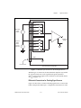
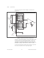


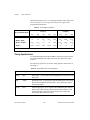

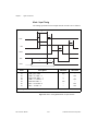
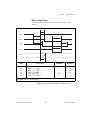

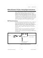
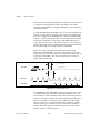
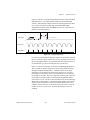

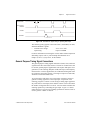


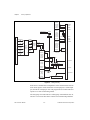
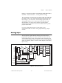


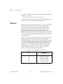
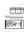


![[Unlocked] SC-2042](http://vs1.manualzilla.com/store/data/005660029_1-1367986a5e7a7fe673239a9957384234-150x150.png)