1
Testing of threshold logic latch based hybrid circuits by Yang Hu A Thesis Presented in Partial Fulfillment of the Requirements for the Degree Master of Science Approved September 2013 by the Graduate Supervisory Committee: Sarma Vrudhula, Chair Hugh Barnaby Shimeng Yu ARIZONA STATE UNIVERSITY December 2013 ABSTRACT The advent of threshold logic simplifies the traditional Boolean logic to the single level multi-input function. Threshold logic latch (TLL), among implementations of threshold logic, is functionally equivalent to a multi-input function with an edge triggered flip-flop, which stands out to improve area and both dynamic and leakage power consumption, providing an appropriate design alternative. Accordingly, the TLL standard cell library is designed. Through technology mapping, hybrid circuit is generated by absorbing the logic cone backward from each flip-flip to get the smallest remaining feeder. With the scan test methodology adopted, design for testability (DFT) is proposed, including scan element design and scan chain insertion. Test synthesis flow is then introduced, according to the Cadence tool, RTL compiler. Test application is the process of applying vectors and the response analysis, which is mainly about the testbench design. A parameterized generic self-checking Verilog testbench is designed for static fault detection. Test development refers to the fault modeling, and test generation. Firstly, functional truth table test generation on TLL cells is proposed. Before the truth table test of the threshold function, the dependence of sequence of vectors applied, i.e., the dependence of current state on the previous state, should be eliminated. Transition test (dynamic pattern) on all weak inputs is proved to be able to test the reset function, which i is supposed to erase the history in the reset phase before every evaluation phase. Remaining vectors in the truth table except the weak inputs are then applied statically (static pattern). Secondly, dynamic patterns for all weak inputs are proposed to detect structural transistor level faults analyzed in the TLL cell, with single fault assumption and stuck-at faults, stuck-on faults, and stuck-open faults under consideration. Containing those patterns, the functional test covers all testable structural faults inside the TLL. Thirdly, with the scope of the whole hybrid netlist, the procedure of test generation is proposed with three steps: scan chain test; test of feeders and other scan elements except TLLs; functional pattern test of TLL cells. Implementation of this procedure is discussed in the automatic test pattern generation (ATPG) chapter. ii TABLE OF CONTENTS Page LIST OF FIGURE ............................................................................................................. vii LIST OF TABLES ............................................................................................................. ix CHAPTER 1. INTRODUCTION ................................................................................................... 1 1.1 Basic of Threshold Logic Latch ...................................................................... 1 1.1.1 Introduction to threshold function ........................................................ 2 1.1.2 Structure of TLL cell ............................................................................. 3 1.1.3 Signal assignment to TLL inputs .......................................................... 5 1.1.4 TLL standard cell library development ................................................. 6 1.1.5 Introduction to the TLL based hybrid circuit ........................................ 7 1.2 Introduction To Testing Of Digital Circuits .................................................... 8 2. DESIGN FOR TESTABILITY FOR THRESHOLD LOGIC LATCH BASED CIRCUITS ................................................................................................................. 14 2.1 Design Of TLL With Scan ............................................................................ 14 2.2 Manual Scan Insertion For Non-scan Netlist ................................................ 16 2.3 Synthesis With Scan Insertion ...................................................................... 17 2.4.1 Read the library ................................................................................... 19 2.4.2 Attributes setup ................................................................................... 19 iii CHAPTER Page 2.4.3 Read HDL files and elaborate design ................................................. 20 2.4.4 Constraints setup ................................................................................. 21 2.4.5 Optimization strategy setup ................................................................ 22 2.4.6 DFT setup ............................................................................................ 22 2.4.7 Synthesize to generic logic ................................................................. 23 2.4.8 Run DFT rule check ............................................................................ 23 2.4.9 Fix violations ...................................................................................... 24 2.4.10 Synthesize design and map to scan ................................................... 24 2.4.11 DFT configuration constraints setup ................................................. 25 2.4.12 Connect the scan chain...................................................................... 25 2.4.13 Run incremental optimization ........................................................... 26 2.4.14 Export the design .............................................................................. 26 2.4.15 Examples ........................................................................................... 26 3. TEST APPLICATION OF THRESHOLD LOGIC LATCH BASED CIRCUIT ... 29 3.1 Parameterized Generic Self-Checking Verilog Testbench Design ................ 29 3.2 Testing Example of Hybrid Datapath Circuit ............................................... 31 4. TEST DEVELOPMENT OF THRESHOLD LOGIC LATCH BASED DESIGN 33 4.1 Functional Test On The TLL Cell ................................................................. 33 4.1.1 Two-pattern reset function test ............................................................ 35 iv CHAPTER Page 4.1.2 Dynamic pattern reset function test .................................................... 36 4.1.3 Conclusion of functional test on the TLL cell .................................... 41 4.2 Structural Fault Test On The TLL Cell ......................................................... 42 4.2.1 Fault analysis on the part of differential amplifier .............................. 44 4.2.2 Fault analysis on the part of input and threshold network .................. 47 4.2.3 Fault analysis on the part of discharge devices ................................... 48 4.2.4 Fault analysis on the part of clock buffer ............................................ 50 4.2.5 Conclusion of structural fault analysis ................................................ 52 4.3 Test Generation Of Hybrid Circuit ................................................................ 53 5. AUTOMATIC TEST PATTERN GENERATION FOR HYBRID CIRCUITS ..... 56 5.1 Encounter Test ATPG Flow........................................................................... 56 5.1.1 Build model ......................................................................................... 57 5.1.2 Edit model ........................................................................................... 58 5.1.3 Build testmode .................................................................................... 58 5.1.4 Verify Test Structures .......................................................................... 58 5.1.5 Build fault model ................................................................................ 59 5.1.6 Create tests .......................................................................................... 60 5.1.7 Commit tests ....................................................................................... 60 5.1.8 Write vectors ....................................................................................... 60 v CHAPTER Page 5.1.9 Report faults ........................................................................................ 61 5.2 Python ATPG Script For Hybrid Circuits ..................................................... 61 5.2.1 Re-synthesize hybrid netlist to CMOS netlist ..................................... 64 5.2.2 Generate the logic model edit file ....................................................... 68 5.2.3 Find in CMOS netlist the corresponding wire names for each TLL input ...................................................................................................................... 69 5.2.4 Build static and dynamic pattern fault model for TLL cells ............... 73 5.2.5 Run ATPG and the testbench .............................................................. 75 6. CONCLUSIONS AND FUTURE WORK ............................................................ 78 REFERENCES ................................................................................................................. 79 vi LIST OF FIGURE Figure Page 1. Structure of the TLL cell [8]. .......................................................................................... 3 2. Different cuts replaceable by the TLLs [8]. .................................................................... 8 3. General structure of sequential logic [9]. ........................................................................ 9 4. A mux-based scan flip-flop: (a) its symbol, (b) a transistor level implementation [11]. ................................................................................................................................... 10 5. A level sensitive scan flip-flop: (a) its symbol, (b) a transistor level implementation [12]. ....................................................................................................................................11 6. Scan chain configuration............................................................................................... 12 7. Schematic of TLL with scan. ........................................................................................ 14 8.Flow chart of test synthesis [21]. ................................................................................ 18 9. Post-synthesis schematic with scan insertion. .............................................................. 26 10. Left half part of the post-synthesis schematic with scan insertion. ............................ 27 11. Right half part of the post-synthesis schematic with scan insertion. .......................... 27 12. Post-synthesis schematic without scan insertion. ....................................................... 28 13. Structure of the testbench. ........................................................................................... 29 14. Fault initialization example 1...................................................................................... 37 15. Fault activation example 1. ......................................................................................... 38 16. Fault initialization example 2...................................................................................... 39 vii Figure Page 17. Fault activation example 2. ......................................................................................... 40 18. Model of the differential amplifier part. ..................................................................... 44 19. Model of the input and threshold network. ................................................................. 47 20. Model of the discharge devices. .................................................................................. 48 21. Model of the clock buffer. ........................................................................................... 50 22. General structure of a hybrid cone. ............................................................................. 53 23. Test generation procedure for hybrid circuits. ............................................................ 54 24. Encounter Test ATPG Flow [22]. ................................................................................ 57 25. Python automation flow of ATPG for generic hybrid circuits. ................................... 63 26. Step 1: Re-synthesize to the CMOS netlist. ................................................................ 64 27. Re-synthesize the TLL cell to CMOS gates. ............................................................... 66 28. Step 2: Generate the logic model edit file. .................................................................. 68 29. Step 3: Find the wires in the CMOS netlist correspond to the original TLL inputs. .. 71 30. Step 4: Build static and dynamic pattern fault model for TLL cells ........................... 73 31. Step 5: Run ATPG and the testbench .......................................................................... 75 32. Fault types under consideration. ................................................................................. 76 viii LIST OF TABLES Table Page 1. Truth table of the function F=a+bc. ................................................................................ 6 2. The number of threshold functions each TLL cell can realize. ....................................... 7 3. Test vector example for the two-stage 4-bit hybrid multiplier. ..................................... 32 4. Part I : Fault analysis on differential amplifier part. ..................................................... 45 5. Part II : Fault analysis on differential amplifier part. .................................................... 46 6. Fault analysis on discharge device part......................................................................... 49 7. Fault analysis on clock buffer part. ............................................................................... 51 ix CHAPTER 1 INTRODUCTION 1.1 BASIC OF THRESHOLD LOGIC LATCH Research on threshold logic has been started since 1943, where the mathematical model of threshold logic gates was proposed for the first time [1]. To express the Boolean function f ( x1 , x2 ,..., xn ) , it used the sign function of the difference of weighted sum and n the threshold value, that is, sgn( wi xi ) . It is promising that threshold logic greatly i 1 simplifies the Boolean logic, from which the area, performance, and power benefit. In 1971, the book [2] about the research on threshold logic and its application was published. The lack of appropriate implementation slows the pace of the relevant research. However, recent years, as discussed in the survey [3], three main types of VLSI implementation of threshold logic are proposed, including capacitive, conductance, and differential solutions. Capacitive solutions contain switched capacitor and the floating gate, with the drawback of required keeper [4]. Conductance solution relies on the static current [5], with the demerit of static power consumption. Comparatively, the differential solutions outperform the other two types, providing better area and power consumption. The paper proposed the threshold logic gate based on a latch-type differential comparator, which achieved lower power [19]. The threshold logic latch (TLL) architecture was proposed [20] to have low leakage power and high performance. Later, as presented in the paper [6], adoption of TLL gates improves both area and total power by a factor of up to 1.5 1 and reduces leakage power by a factor of up to 2.3 in the experiment of the pipelined multipliers. On the other hand, there are numerous papers and patent solving problems in threshold logic synthesis [16-18]. Recently, the paper [7] provided an efficient heuristic procedure based on binary decision diagram (BDD) [15] for threshold decomposition, i.e., identifying the threshold function from the given Boolean function. Finally, the design method of a standard cell library of TLL and the relevant technology mapping were proposed in the paper [8]. 1.1.1 Introduction to threshold function The model of circuit under test is based on the paper [6-8]. If the on and off set of a Boolean function f ( x1 , x2 ,..., xn ) is linearly separable, it can be called threshold function. In other words, the threshold function is identified if there exist a certain set of weights ( w1 , w2 ,..., wn ) and the threshold value T such that f ( x1 , x2 ,..., xn )=1 if and n only if w x i 1 can be i i T . For example, f (a, b, c, d , e) ac(b d e) de(a bc) ab(d e) transformed to the threshold function with the weight vector ( wa 2, wb 1, wc 1, wd 1, we 1) and T 4 [8]. It is obvious that this threshold logic is of single level which greatly reduces the logic and implementation complexity, compared to its multi-level Boolean version. 2 1.1.2 Structure of TLL cell M1 M2 M3 M4 N1 N2 M5 clk M6 N3 M11 N4 M7 ... inn-1 CP in1 clk M8 N5 N6 in0 inn clk M12 inn+1 ... in2n-1 clk Figure 1. Structure of the TLL cell [8]. Figure 1 shows the schematic of the differential part of the TLL cell. Note that the N1 and N2 should further connect to the latch which keeps its output when both inputs are high and the output Q of the latch is equal to the value of N2 if either N1 or N2 is pulled down. 3 The inputs of the TLL cell contain the input network (network in the left side) (in0 , in1 ,..., inn 1 ) , the threshold network (network in the left side) (inn , inn 1 ,..., in2 n 1 ) , and the controlling clock input CP. The only observable TLL output is the output Q of the latch. The TLL has two operation phases, reset and evaluation phase, when CP=0 and CP=1 respectively. In reset phase, clk=0. N5 and N6 are discharged through M11 and M12, turning on the reset PMOS M1 and M4. Hence N1 and N2 are pulled up with the latch keeping its value. In evaluation, on the other hand, CP rises, so does clk. Discharge devices M11 and M12 turn off. Next, N5 and N6 are charged through input and threshold networks. The charging speed of N5 and N6 is determined by the impedance of the network in each side. The comparison of the network impedances implements the inequation of weighted sum and the threshold value. For instance, if the input network has lower impedance than that of the threshold network, N5 charges faster than N6. Then M7 turns on earlier than does M8, so that N1 discharges faster than N2. When N1 is pulled below the threshold of M3, N2 is charged, preventing the discharge of N2 and pulling it back to VDD. Eventually, N1=0 and N2=1. Due to the function of the latch, the Q is set to 1. 4 1.1.3 Signal assignment to TLL inputs An example of TLL5_32 cell is illustrated [8]. To implement the function of F a b c , its threshold version, f (a, b, c) 4 a 2 b 2 c 3 , is obtained by threshold decomposition. Each value of one in this inequation stands for a conducting PMOS. Too many PMOS input transistors are needed in the left side and three PMOS are always on in the right side, if the signal assignment is directly a, a, a, a, b, b, c, c | 0,0,0 . Considering a 1 a , the inequation can be optimized to another variation, f (a, b, c) 3 a b c (1 a ) (1 b) (1 c) . Hence the signal assignment is a, a, a, b, c | a, b, c,1,1 . In this case, the input PMOS transistors needed for both sides reduce to five. And the power loss due to always conducting PMOS is eliminated. Thus the cell TLL5_32 is selected, where the five means that each of the input network and threshold network has five PMOS and the worst case comparison of two weighted sums is three versus two. Table 1 shows the truth table. 5 Table 1. Truth table of the function F=a+bc. a b c Weighted sum of the input network Weighted sum of the threshold network Output Q 0 0 0 0 3 0 0 0 1 1 2 0 0 1 0 1 2 0 0 1 1 2 1 1 1 0 0 3 2 1 1 0 1 4 1 1 1 1 0 4 1 1 1 1 1 5 0 1 The optimal signal assignment (OSA) is proposed in [8], which eliminates the always on PMOS, maximizes the worst case noise margin, and minimizes the worst case delay and power. 1.1.4 TLL standard cell library development The TLL library is designed in [8], which includes four cells, TLL-3, 5, 7, and 9, according to the number of transistors in the network each side. For each cell, the number of threshold functions it can implement is demonstrated in Table 2. Altogether, the four cells can implement 72 threshold functions, with the great reduction in labor and library size. Alternatively, each cell can be optimized separately for each possible worst case input. Consequently, the actual standard cell library developed contains ten cells, 3_21, 6 5_21, 5_32, 7_21, 7_32, 7_43, 9_21, 9_32, 9_43, and 9_54, where the last two digits represent the worst case input configuration. Table 2. The number of threshold functions each TLL cell can implements. TLL Cell TLL-3 TLL-5 TLL-7 TLL-9 TOTAL Functions 3 8 18 42 72 1.1.5 Introduction to the TLL based hybrid circuit Hybrid circuit is generated by selecting suitable sub-circuits ending with a flip-flop and replacing them with functionally equivalent TLL cells. This process is called hybridization [8]. The procedure is that for each flip-flop and its feeder cone, enumerate all possible cuts,decompose the function of each cut, and select the decomposition which achieve the smallest feeder. 7 Figure 2. Different cuts replaceable by the TLLs [8]. Figure 2 shows the two different cones replaced by TLL-3 and TLL-5. In most cases, there is a combinational logic block as the feeder. 1.2 INTRODUCTION TO TESTING OF DIGITAL CIRCUITS Modern digital circuits can be considered as combinations of flip-flops and combinational logic blocks. Main steps of testing are test development and test application. Test development refers to fault modeling, test vector generation and fault simulation. Test application, on the other hand, is about test process itself. For example, apply the test vectors to the primary inputs or scan inputs, timing control, and response analysis. [9] For a combinational logic or a pipelined datapath, the primary output is only the calculation result of the primary input. There is no dependence of current vector on the previous vector. In this case, all vectors can be applied in some sequence. 8 x1 z1 xn zm Combinational Logic Block y1 Y1 yk Yk Q D Clk Q Q D Clk Q Figure 3. General structure of sequential logic [9]. For the general structure of sequential circuit, as shown in Figure 3, the state machine takes place. The current state input <y1:yk>, which is also the state output <Y1:Yk> registered in the previous clock cycle, and the primary input <x1:xn> determine the current state output <Y1:Yk> and the primary output <z1:zm>. Directly testing sequential circuits has the problem of setting and checking the state of the system [10]. Scan test offers controllability and observability on such flip-flops. It breaks feedback loops in sequential circuits, simplifying the problem of sequential test to test of combinational blocks. However, the area and performance are the cost of scan. Optimization can be done to reduce the impact. Overall, using scan to test is a good tradeoff, for the necessity of testability. 9 Scan elements are usually flip-flops or latches with scan functions added. Normal mode refers to the normal calculation or propagation as what the ordinary flip-flops or latches do. While scan mode, or called test mode, triggers the scan input rather than the normal input to get in so that the connected scan chain shifts its value from the scan in pin of the chain further out to the global scan out pin. TE DI 0 TI 1 D Q CLK (a) TE DI CLK CLK Q CLK TI CLK CLK CLK CLK CLK (b) Figure 4. A mux-based scan flip-flop: (a) its symbol, (b) a transistor level implementation [11]. 10 Figure 5. A level sensitive scan flip-flop: (a) its symbol, (b) a transistor level implementation [12]. Figure 4 shows a design of the mux-based scan flip-flop, in which a mux is added before the data inputs of the flip-flop. Figure 4 (a) shows the common symbol for mux-based scan flip-flops. Figure 4 (b) implements this mux using transmission gates. The test enable (TE) determines whether the circuit works in normal mode or in test mode. In other words, TE controls the flip-flop to register the value from whether the data input DI or the test input TI. The single clock (CLK) signal controls the pace of flip-flops in both modes. The cost is the additional multiplexer. 11 Figure 5 introduces a level sensitive scan flip-flop for a single latch sequential circuit. In Figure 5 (a), the common symbol is shown. Figure 5 (b) introduces an implementation of level sensitive scan flip-flop. Both L1 and L2 are positive latches. In normal mode, non-overlapping clocks C and B control and take the value of data input D, with A kept low. +L1 can be used as normal mode output in a single-latch sequential circuit, while in double latch design +L2 is used. In test mode, non-overlapping clocks A and B control and take the value of test input I, with C kept low. Only +L2 is used as the output due to the operation of shift registers. This design eliminates the multiplexer but the clocks complicate the job of control. Scan Output Pin TE DI TE 0 D TI 1 DI 0 TI 1 Q D Clk Q Clk Q Q TE DI TE 0 D TI 1 DI 0 TI 1 Q Clk Q D Combinational Logic Block TE 0 DI D TI 1 Clk Q TE DI Q 0 Q D TI Clk Q 1 Q Clk Q Scan Input Pin Figure 6. Scan chain configuration. 12 Figure 6 shows the general scan chain configuration. The dashed lines with arrow constitute the scan chain, while the solid lines with arrow represent the normal mode connection. To make use of the scan chain, these scan elements should be configured into test mode. Then the scanned test vectors get shifted into the chain through the scan input pin. The minimum number of clock cycles for the test mode is determined by the bigger one among the distance of furthest scan element seen from scan input pin to drive the combinational block and the distance of furthest scan element seen from scan output pin to receive the data from the combinational block. Between the current scan mode cycles and the next ones, the normal mode cycle should be inserted. So the data gathered from the output of the combinational block would get shifted out of the scan out pin as the new vector shifts in. This can be complicated if, for multiple combinational blocks, different numbers of test vectors or multiple scan chains are needed. 13 CHAPTER 2 DESIGN FOR TESTABILITY FOR THRESHOLD LOGIC LATCH BASED CIRCUITS 2.1 DESIGN OF TLL WITH SCAN M1 M2 M3 M4 N1 N2 M5 clk M11 TE M13 M9 TI M15 clk M17 M6 TEB TEB inn-1 ... in1 TE M16 TIB M18 clk M12 clk M10 M7 TEB M14 M8 N5 N6 in0 inn TI CP inn+1 TIB ... TE in2n-1 TEB TEB Figure 7. Schematic of TLL with scan. Figure 7 shows the schematic of the scan version of TLL. M13, M15, M17, M14, M16, and M18 form the testing branch for each side. On the other hand, M9, M7, M10, and M8 can be called as normal branch. In test mode, test enable (TE) is asserted so that the M9 and M10 are open, breaking the relation of N1, N2 to the inputs, in 0 to in2n-1. 14 Then the charge in N1 or N2 will be flown through either left or right branch under the control of test input (TI) signal. Bottom clock gate ensures that this scan element works only on evaluation phase, while not impacting the charge during reset phase. Since the output Q of the TLL is directly controlled by and follows TI, it plays a shift register role. In normal mode, TE signal is de-asserted, turns off the two testing branches. M9 and M10 are on and output Q of TLL depends on inputs. Another change compared to TLL without scan is the input PMOS transistor added to both input network and threshold network. Its gate connects to TEB. This addition ensures that the reset PMOS M1 and M4 can be properly turned off in evaluation phase and test mode. If, in test mode, either input network or threshold network has no PMOS on, in reset phase N5 and N6 are pulled down to reset N1 and N2. In the following evaluation phase, either N5 or N6 remains low and the corresponding reset PMOS keeps working, influencing the equation of Q and TI. Added PMOS in both sides eliminate this problem, making sure that N5, N6 gets pulled up in evaluation phase of test mode. The size of the testing branch should be small, which leads to little cost in delay, area and power. As the normal branch can be shut off in test mode, there is no need for a big driving capability. In most cases, minimum transistor size suffices. 15 2.2 MANUAL SCAN INSERTION FOR NON-SCAN NETLIST Scan insertion is the transformation from non-scan circuit to scanned version of it, where one or more scan chains are connected. Given the netlist of a circuit, replace sequential elements with scan elements. Each scan element has two additional pins, test enable (TE) and test input (TI). The following three pins are added for test mode operation. GTE is the global test enable input. DFT_sdi and DFT_sdo are the scan input and output pin. Since the sequential elements here consist of flip-flops and TLL cells, their scanned version should be prepared beforehand. For the RTL of TLL cells, a judgment sentence is added. Depending on the TE value, either TI or normal function calculation is applied to the latch and assigned to Q. Similar change is also needed for the scanned D flip-flops in RTL. Manual scan insertion provides the freedom to place the scan chain. Number of scan chains, partial or full scan, etc., impacts the connection of the scan chain. To begin with, the DFT_sdi pin is connected to the TI of first scan element. Then the output Q of each scan element is connected to TI of the next scan element, until the output of last one is assigned to the DFT_sdo pin. Moreover, hold violation along the scan chain should be checked by monitoring both rise and fall transitions. If metastability occurs, buffers should be added in the scan path. 16 2.3 SYNTHESIS WITH SCAN INSERTION Manual scan insertion is custom but time-consuming. Modern CAD tools can conveniently take part in scan insertion, as one task during synthesis. Test synthesis transforms the raw RTL design into the optimized gate level netlist with all the desired DFT scan elements mapped and scan chain connection, which meets all constraints. All the examples and commands illustrated in this part are based on Cadence RTL Compiler. To control the tool, Tcl scripts are programmed to fulfill tasks in the top-down flow as is shown below. [21] 17 Start Read the library Attributes setup Read HDL files and elaborate design Constraints setup Optimization strategy setup DFT setup Synthesize to generic logic Run DFT rule check Fix violations Synthesize design and map to scan DFT configuration constraints setup Connect the scan chain Run incremental optimization Meet all constraints Export the design End Figure 8.Flow chart of test synthesis [21]. 18 Figure 8 shows the flow chart for test synthesis. Detailed description for each step is listed below [21]. Note that the following description is based on mux-based scannable flip-flops as scan elements and is not a complete introduction. Only the most commonly used are presented. 2.4.1 Read the library The library adopted for synthesis with its path should be specified. 2.4.2 Attributes setup Attributes can be set to control the synthesis process in detail. Among the numerous types of attributes, three most commonly used types of attributes are described below. Libcell attributes setup. Each library cell has its associated attributes to be set. This step mainly refers to the attribute of avoid. If some cells are supposed to be avoided by the mapper, the attribute of avoid of those cells should be set true. It’s often the case that not all cells are wanted. For example, whether use TLL cells or not can be controlled in this way. The expression, find –libcell, is useful to specify the name of the desired cells to select. 19 Input and output attributes setup. When the design is exported, the command, write_hdl, will generate the structural netlist. There are attributes specifying rules for output Verilog. Examples are whether to include the implicit wires in the netlist, and whether to create dummy wires for unconnected pins, etc. Elaboration attributes setup. First, for elaboration, there are attributes to configure the naming style of individual bits in registers or arrays, module name in parameterized modules, instance name in a for-generate statement. All internal names can be elaborated in the alphanumeric habit. Second, issuing error messages or not is controlled by relevant attributes. Error examples are unresolved references and latch inferred during elaboration. Third, tracking of the RTL source code can be enabled, which includes track of filenames, and line numbers for each instance. Information kept before any optimization is useful for later procedures, such as error messaging and DFT violation warning. Synthesis attributes setup. Rules for synthesis can be specified by setting attributes. 2.4.3 Read HDL files and elaborate design Elaboration takes the raw HDL file, creates data structure internally, infers registers, performs high level HDL optimization, and links the cell to the reference in the library file, making it into an appropriate form for synthesis and constraint operations. 20 To read the HDL files in, run the command, read_hdl. Note that tracking of the source code should be allowed by setting true the attribute, hdl_track_filename_row_col. Then run the command, elaborate. Thus the RTL compiler elaborates the design. 2.4.4 Constraints setup To setup the timing constraints, the clock signal should be defined, using command, define_clock. Clock domain can be created as a group of synchronous clocks. Here the constraint of period should be specified. Clock edges, skew, transition or latency can also be defined if needed. Similarly, input and output delays can be defined with command of external_delay. On the other hand, design rule constraints need to be set. Design rule constraints are physical requirement for synthesis process. It consists of three constraints, maximum capacitance per net, maximum fanout per gate, and maximum transition of a signal. Three corresponding attribute, max_fanout, max_capacitance, and max_transition, can be set to the proper value. Any violations are reported when design is exported, by the command, report design_rules. Other design constraints include external driver and load constraints, operating condition specifications, timing exception setup, etc. 21 2.4.5 Optimization strategy setup Optimization strategy is made up of numerous optimization settings before the synthesis. Most commonly used settings are preserve attribute and group and ungroup operations. In default optimization, all logic parts or objects may change. If some logic or objects are supposed to keep untouched, while others can be optimized freely, the preserve attribute of those instances can be set true to avoid any change. For example, TLL cell should be kept during synthesis. So the preserve attribute of all TLL cells should be true. Group and ungroup operation changes the design hierarchy. Subdesign instances can be grouped into anther single subdesign, while ungrouping flattens a hierarchy level. Another choice is automatic ungrouping. Ungrouping criteria such as timing, and area and ungrouping effort level can be configured. 2.4.6 DFT setup DFT setup contains basic scan style setup, scan chain specification, and DFT rule specification. First of all, scan style refers to using either mux-based flip-flop or level sensitive scan elements. Then, the shift enable signal or scan clock signal should be defined and assigned to a pin using the following command, define_dft. There are other settings dependent on the specific design. 22 2.4.7 Synthesize to generic logic According to the design constraints, the command, synthesize –to_generic, perform an RTL optimization. Since elaboration produces don’t care logics, undesirable DFT violation appears under DFT rule check. Those don’t care logics can be eliminated by synthesizing to generic logic. 2.4.8 Run DFT rule check During the DFT rule check, auto-identification of the test clock and test mode signals should be prevented. This can be done by setting false the attributes, dft_identify_top_level_test_clocks and dft_identify_test_signals. After auto-identification has been disabled, run DFT rule check using the command, check_dft_rules. The DFT rule contains two aspects. First, check if the clock pin of each flip-flop is controlled from primary input or defined test clock. In other words, violation happens when any clock pins of flip-flops are uncontrollable. Second, check if all asynchronous pins of flip-flops can be assigned to be in their idle state when in test mode. Only those flip-flops which pass the DFT rule check can be mapped to scan elements and included in the scan chain. DFT condition and result of this check of each flip-flop is reported by the command, report dft_registers. 23 2.4.9 Fix violations If any clock violation or asynchronous violations exist, they need to be fixed using the command, fix_dft_violations. Then check the DFT rule again and then fix until no violation appears. To report the violations, the following command, report dft_violations, can be used. 2.4.10 Synthesize design and map to scan To control the mapping of non-scan flip-flops to scanned flip-flops, the attribute, dft_scan_map_mode, should be set. In most cases, mapping only those which pass the DFT rule check is the most appropriate scheme. Other choices are preserving and maping all. For the flip-flops during synthesis, the scan in pin is usually connected to the data output pin and the test enable pin is in its inactive value. For any existing scan chains, they need to be preserved. Then the DFT setup can be reported by the command, report dft_setup, after all settings are set. Next, synthesize the design and map the flip-flops to their scan version as described in the library, with the optimization goal of providing smallest possible implementations which meets all constraints. Check the report and take care of the warnings. 24 2.4.11 DFT configuration constraints setup Scan chain connection has variant configuration choices. For example, the minimum number of scan chains, and maximum length of scan chains can be configured. Also whether to allow mixture of rising and falling edge triggered flip-flops can be determined. In addition, the top-level scan chains can be defined. Finally, report the configuration setup. 2.4.12 Connect the scan chain The scan chain will be connected using the command, connect_scan_chains. It connects scan elements, which pass the DFT rule check, into chains. If only the chains defined in the DFT configuration constraint are allowed for connection, use the command, chains chain_list. Aside from what has been defined in the DFT configuration constraint, if new scan chains are allowed to be added, the following command needs to be included, auto_create_chains. When scan chain connection finishes, the scan chain and DFT setup information are supposed to be reported. 25 2.4.13 Run incremental optimization When the design has been mapped, incremental optimization preserves the current implementation and changes only when the new procedure brings about any improvements. The timing problem resulted from scan chain connection with example of hold time violations can be resolved by this optimization. The relevant command is synthesize –incremental. If the resulting implementation after optimization does not meet all the constraints, go to the constraints and optimization strategy setup again carefully and practically. 2.4.14 Export the design Report timing, critical path, gates, power and area details. Generate gate-level netlist, SDC file for place and route, and the scandef file. Moreover, report important DFT files with examples of design rule violations, scan chain information, status of registers, DFT setup, and DFT violations. 2.4.15 Examples Figure 9. Post-synthesis schematic with scan insertion. 26 Figure 10. Left half part of the post-synthesis schematic with scan insertion. Figure 11. Right half part of the post-synthesis schematic with scan insertion. Figure 9, Figure 10, and Figure 11 show the gate level schematic after proper test synthesis, taking the four-bit adder as an example. As can be seen, the flip-flops connect each other in a line, making up the scan chain. The two 4-bit value being added are a[3:0] and b[3:0]. The 5-bit sum is p[4:0]. DFT_sdi_1 and DFT_sdo_1 are the global scan input and output. Global test enable (GTE) signal controls each flip-flop to perform as a shift register in the chain or a separated register connecting the primary input or output. 27 Figure 12. Post-synthesis schematic without scan insertion. As a comparison, Figure 12 shows the gate level schematic after synthesis without scan connection, taking the four-bit adder as an example. As can be seen in Figure 12, the combinational logic blocks are sandwiched between the 8-bit input flip-flops and the 5-bit output flip-flops. Each flip-flop is self-connected, thus no scan chain formed. The only controlling signal is the clock signal. 28 CHAPTER 3 TEST APPLICATION OF THRESHOLD LOGIC LATCH BASED CIRCUIT 3.1 PARAMETERIZED GENERIC SELF-CHECKING VERILOG TESTBENCH DESIGN In this chapter, the way of using those vectors to test circuits is emphasized. Note that the test application scheme here only considers static faults. Since the circuit under test can be of any bits of input or output, multiple stage or single stage, datapath or with feedback path, and the test itself can be functional truth table test or any other type of test, it is practical to build a parameterized all-purpose test bench with the feature of self-checking, in other words, do the response analysis itself. For ease of explanation, circuit under test is assumed to be with single scan chain. Figure 13 shows the structure of the testbench. Each box below corresponds to one procedural block. Set the input parameters Clock control Reading test vectors Primary input control Response analysis Figure 13. Structure of the testbench. First of all, parameters provide flexibility of the testbench. On one hand, the scan chain should be configured. Before further discussion about each parameter, some concept of scan shift policy is imperative to be illustrated [9]. It is commonly used that along the scan chain, scan elements which provide inputs to the combinational logic 29 (kernel) are called driver, while those which receive outputs of the kernel are called receiver. Starting from the scan in pin to the scan out pin, the distance between the scan in pin to the last driver is the minimum clock cycles required to scan in all vectors, which is denoted as SCin. Similarly, the distance between the first receiver and the scan out pin is the minimum clock cycles needed to scan out all response, which is denoted as SCout. SC denotes the actual clock cycles in scan mode with scanning in and scanning out overlapped. In minimum-shift policy, SC = max (SCin, SCout). But in flush policy, SC equals to the length of the scan chain. Obviously, switching between these two scan shift policy can be done by custom choice of the value of SC. On the other hand, the number of pipeline stages, PPL, determines the normal mode cycles required. For larger circuits, the combinational logic may be divided by the scan chain into different kernels. In order to differentiate the kernels under test, the whole test is sometimes conducted in a successive of test sessions. In such case, PPL should equal to the pipeline stages of the current kernel under test. In addition, parameters like the clock period and number of test vectors are also in need of configuration. Secondly, the test vectors are read from the vector file. Each vector contains its number, the vector to be scanned in, and the expected output vector. Then they are stored in arrays and applied in proper time. 30 Thirdly, primary input controller mainly controls the scan in signal (SI) and test enable signal (TE). The scan mode SC cycles are followed by normal mode PPL cycles. Both SI and TE signals are assigned to new value in the inactive edge of the clock to avoid metastability. In scan mode, SI is controlled by the stored scan input vector and change cycle by cycle to shift in and the TE keeps asserted. In normal mode, TE stays de-asserted. Fourthly, response analysis plays an important role. The response of the first vector appears after SC + PPL cycles and last for SCout cycles. Similarly, there are SC + PPL cycles between the starting bits of two contiguous responses. Note that the response should be observed in falling edge (inactive edge) of the clock to avoid metastability. 3.2 TESTING EXAMPLE OF HYBRID DATAPATH CIRCUIT As datapath circuit does not include any feedback path, its primary outputs merely depend on primary inputs and it has no state input or state output. In other words, it’s not a state machine. Consequently, the outcome of datapath circuit test does not depend on the sequence of the vectors applied, which enable the functional truth table test by connecting all the primary inputs and outputs as the scan chain. Besides, datapath circuit can have multi-stage pipeline. 31 Take the example of a functional test of the two-stage 4-bit hybrid multiplier. The parameters need to be set correctly. As is easily analyzed, the SCin and SCout are 8 and 7 respectively, due to the fact that the scan chain is designed to stretch through each primary input scan element and then pass each primary output scan element. Obviously, the number of pipeline stages, PPL, should be set to 2 cycles of normal mode, after which the exact outcome of the combinational logic can be latched to the output half of the scan chain. The response of the first vector appears after 10 (SC + PPL) cycles and last for 7 (SCout) cycles. Similarly, there are SC + PPL cycles between the starting bits of two contiguous responses. Table 3 shows some vectors examples, where the first digit in the right hand side is the least significant bit. The input vector represents two 4-bit multiplier factors, as divided by a space in the middle. However, the output vector stands for an 8-bit product. If the test fails to pass all vectors, the testbench will output the very vector which produces the response different from the expected one. Table 3. Test vector example for the two-stage 4-bit hybrid multiplier. # 1 2 3 4 5 Input vector Expected output vector 0000 0000 0001 0001 0011 0010 0000 0001 0011 0001 00000000 00000001 00000110 00000000 00000011 32 CHAPTER 4 TEST DEVELOPMENT OF THRESHOLD LOGIC LATCH BASED DESIGN 4.1 FUNCTIONAL TEST ON THE TLL CELL All following discussion in this thesis about testing of hybrid circuits is based on full scan scheme [9], meaning that all the registers or latches in the netlist should be connected into the scan chain. So each kernel is single stage and only one cycle is required for the normal mode. In a real circuit, the TLL cell has fixed input connection and implements a certain function. So the direct way to test is applying vectors of the whole truth table. Here suppose the inputs of the TLL cell can be controlled. And the only observable output is the output of the TLL cell, i.e., Q. Two different types of inputs for TLL can be defined. Weak inputs refer to those input vectors which produce the minimum difference between the weighted sum in the input network and that in the threshold network. In real cases, the weak inputs can be identified by searching for vectors with one-difference between the two sides, which tend to fail more easily. Taking account of single fault assumption, if the weighted sum increases or decreases by value of one due to a fault in either input network or threshold network, only the weak inputs may fail and produce an equation between weighted sums of two sides. Strong inputs, on the contrary, produce the difference larger than one, among which the strongest inputs refer to those produce the maxim difference. 33 Another pair of terms is defined for convenience of discussion. One inputs mean any input vectors which result in output Q=1, where the weighted sum in the input network is larger than that of the threshold network. Similarly, zero inputs refer to any input vectors which make output Q=0, where the weighted sum in the input network is smaller than that of the threshold network. To make the discussion of test vectors understood, an example of TLL5_32 cell is illustrated in chapter 1.1.3 and commonly used in this chapter. Table 1 shows the truth table for this function. Here (x,y) denotes that the input network has x transistors on and the threshold network has y transistors on. It can be identified that the weak inputs are (1,2), (2,1), (3,2), and the strongest inputs are (0,3), (5,0). Besides, the one inputs include (2,1), (3,2), (4,1), (5,0), while the zero inputs contain (0,3), (1,2). One important fault type is the functional reset fault. Reset phase needs to work. In other words, both N1 and N2 in reset phase need to be pulled up to VDD. Since TLL is a sequential circuit, state machine takes part in without successful reset in between evaluations. If the fact that TLL evaluation does not depend on history or last state gets proved, truth table test becomes feasible. To explore the method to ensure that reset really works, transition fault test is introduced. If reset does not work well, in evaluation phase, discharge in the two branches, N1 and N2, fights with the value left in the two branches from previous evaluation, when a transition is supposed to appear in the output. As a result, weak inputs 34 are more likely to fail and the strongest inputs are more likely to cause the next evaluation to fail. As a result, the worst case of the transition fault is that the weak input transits the previous state initialized by the strongest input. 4.1.1 Two-pattern reset function test To conclude the way of testing the reset function, all possible two-pattern vectors with supposed transition in the output and in the following sequence, strongest inputs to weak inputs, can be applied. If the transition can always propagate to the output within certain amount of time, the reset of this TLL cell works. Then the truth table test can be done in any sequence. Table 1 shows the truth table. So if notation of (weighted sum of input network, weighted sum of threshold network) is used, (0,3) -> (3,2) and (5,0) -> (1,2) can be used for reset function test. Note that (5,0) -> (1,2) should be conducted twice for two input vectors of (1,2). After testing for reset function, the remaining three vectors can be applied as the whole truth table should be tested. Limitation of this two-pattern test is that it requires the sequential controllability of TLL inputs and observability of TLL output. For example, the output of the first vector should be observed directly from the primary output or by scanning out its value from the two-pattern test. On the other hand, the two patterns should be applied successively in normal mode. In some cases, the second pattern is unavailable for the TLL input pins. 35 4.1.2 Dynamic pattern reset function test The limitation disables the use of two-pattern reset function test in multi-stage full-scan hybrid circuit. To design a generic scheme, the dynamic pattern reset function test, as is discussed below, should be adopted. Here the dynamic pattern test [31] is the scheme of scanning in the initialized value in the output of TLL, together with the TLL input vector to activate the fault. To make sure the initialization is the strongest, the scan chain and the scan chain test help. Before all the test vectors applied into the scan chain, it is common that the test for the function of scan chain itself should be conducted. This is due to the fact that all vectors for the kernel are derived with the assumption of correct operation of the scan chain. Without the scan chain test, in some extreme scenarios, faults in the kernel and in the scan chain may cancel each other, making the scan chain test necessary from another angle. The vector for scan chain test is normally a sequence of zeros and ones with frequent transitions, which is applied to the scan in pin [31]. It can be either static or dynamic. The test enable signal is held in its asserted value and the output is measured from the scan out pin. Thus any fault induced in the test branch in the TLL cell can be detected. Interestingly, the correct operation guaranteed by the scan chain test provides the most confident initialization. The desired value of initialization can be set by scanning in the fault activation vector with the initialized output bit of that TLL cell. 36 The general reset function test procedure for a TLL cell is as follows. First, find the weak inputs. Second, scan in the weak input with its corresponding initialization bit in the position of the output of the TLL cell. Third, apply the normal cycle. Fourth, scan out the output result of this TLL cell, which can be overlapped with the next weak input vector scanned in. Figure 14. Fault initialization example 1. 37 Figure 14 shows the initialization for a weak input with lower impedance in the input network. The test related signal is set to their asserted value. In the last cycle of the scan mode, the correct initialization bit with the value of zero is stored in the latch. The N1 and N2 is 1 and 0. In the subsequent reset phase, both N1 and N2 are supposed to be pulled up. Faulty reset results in incomplete pull-up for N2. Figure 15. Fault activation example 1. 38 Figure 15 shows the fault activation for a weak input with lower impedance in the input network. The test related signal is set to their de-asserted value. In the normal mode cycle, the discharge in the left branch, as is indicated by the arrow, fights the charge across M2 caused by incomplete reset N2. Only when it wins with correct output stored in the latch can the TLL cell pass this test vector. Figure 16. Fault initialization example 2. 39 Figure 16 shows the initialization for a weak input with lower impedance in the threshold network. The test related signal is set to their asserted value. In the last cycle of the scan mode, the correct initialization bit with the value of one is stored in the latch. The N1 and N2 is 0 and 1. In the subsequent reset phase, both N1 and N2 are supposed to be pulled up. Faulty reset results in incomplete pull-up for N1. Figure 17. Fault activation example 2. 40 Figure 17 shows the fault activation for a weak input with lower impedance in the threshold network. The test related signal is set to their de-asserted value. In the normal mode cycle, the discharge in the right branch, as is indicated by the arrow, fights the charge across M3 caused by incomplete reset N1. Only when it wins with correct output stored in the latch can the TLL cell pass this vector. 4.1.3 Conclusion of functional test on the TLL cell As discussed before, the weak inputs are easier to fail, since it needs to fight against the strongest opposite initial value scanned in, if reset does not work correctly. It is reasonable to assume that the reset function works if all weak inputs pass such dynamic pattern test. The procedure can be concluded as two steps. First, for all weak inputs, do dynamic pattern test. Second, for the remaining vectors in the truth table, that is, all the strong inputs, do static pattern test. Here the static pattern test means the regular static test with the fault activation vector scanned in and without the initialization. 41 4.2 STRUCTURAL FAULT TEST ON THE TLL CELL Chapter 4.1 proposes a functional test on TLL cells. Ideally any fault types or multiple faults which influence the functional operation of the TLL are detected. However, one specific structural fault may mask the fault propagation of another fault, making the declaration of fault-free circuit invalid. For example, when the feeder is tested, if an undetected structural fault inside the TLL cell masks the propagation of one fault in the feeder, the latter one becomes undetected and may propagate the faulty effect to the output under other input configurations. Therefore, it is necessary to delve into the TLL cell and derive the test for structural faults. Transistor level structural fault model is analyzed for the TLL standard cell. It is a reasonable simplification here to note that all the analysis is based on the cell of TLL without scan and all operations are in normal mode. Because the scan related part can be tested functionally in scan chain test separately in the beginning, which is further discussed in the last part in this chapter. All the following discussion is based on single fault assumption and scan test. Every vector proposed is applied in the normal cycle. Dynamic pattern test can be used to provide an initialization and observe a transition, which is commonly adopted for weak inputs, as proposed in chapter 4.1.2. 42 Fault model used here is of static faults including stuck-at faults, stuck-open faults and stuck-on faults. Firstly, stuck-at faults refer to lines always on voltage of VDD or GND, no matter the voltage on the driver or its stem [13]. And if stuck-at fault happens on the stem, all the downstream lines are affected. Note that the stuck-at faults are only modeled on stems and those lines which drive a gate. Stuck-at faults are modeled for those wires which drive the gate of at least one transistor. Secondly, for the stuck-open fault, the transistor keeps open irrelevant to the voltage on its gate. Similarly, for the stuck-on fault, the transistor keeps on irrelevant to the voltage on its gate. [14] Each TLL cell can be divided into 4 parts for convenience of analysis, i.e., differential amplifier, input/threshold networks, discharge devices, and clock buffers. Due to the fact that the latch is merely controlled by N1 and N2 determined jointly by the four parts listed above, the latch is not included. Its full function of four possible output cases, 0->0, 0->1, 1->1, and 1->0, together with the function of test mode related transistors and wires, are tested by scan chain test beforehand. In each part, faults are grouped with same or similar effects, thus sharing the same test set. In other words, they are equivalent faults. Each group is matched with the relevant test method, including the use of current monitor which detects large current caused by DC path for a long enough period of time. 43 4.2.1 Fault analysis on the part of differential amplifier N5P M1 M2 N2P N1P M3 M4 N1 N6P N2 M5 N5 N2N N1N M7 M6 N6 M8 N5N N6N Figure 18. Model of the differential amplifier part. Figure 18 shows the fault model on the differential amplifier part. Here N5 and N6 can be modeled as the stem, since it is controlled by discharge device and input network and threshold network in respectively reset phase and evaluation phase. Due to the different function between the reset PMOS and the pair of NMOS in the bottom, treating N5P and N5N as separated branches is a better way. Besides, each transistor should be modeled and there is no exception. 44 Table 4. Part I : Fault analysis on differential amplifier part. Faults N5P_0; M1_On; M2_On; N2P_0 N5P_1; M1_Open Effect Analysis N1 is always pulled up. Large current when no transistor is on in threshold network. Otherwise, due to positive feedback, Q is always zero. M1 keeps open. Once discharged, N1 cannot be pulled up. N5N_0; M7_Open N5N_1; M7_On M7 keeps open. N1 is always 1. Faulty response Test vector Large current in (3,2) evaluation for (5,0). Q=0 for other one inputs. Q=1 for weak zero dynamic inputs (dynamic pattern pattern). (1,2) Q=0 for one inputs. (3,2) Large current in reset. Q=1 for zero inputs. Large current in evaluation for (0,3). Q=1 for other zero inputs (1,2) N6P_0; M4_On; M3_On; N1P_0 M7 keeps on. Large current in reset. In evaluation, M7 always discharges earlier than M8. Thus Q is always 1. N2 is always pulled up. Large current when no transistor is on in input network. Otherwise, due to positive feedback, Q is always one. N6P_1; M4_Open M4 keeps open. Once discharged, N2 cannot be pulled up. N6N_0; M8_Open N6N_1; M8_On M8 keeps open. N2 is always 1. Q=0 for weak one inputs (dynamic pattern). Q=1 for zero inputs dynamic pattern (3,2) (1,2) Large current in reset. Q=0 for one inputs. Q=1 for zero inputs (3,2) Q=0 for one inputs. (3,2) Q=0 for one inputs. (3,2) M8 keeps on. Large current in reset. In evaluation, M8 always discharges earlier than M7. Thus Q is always 0. M2_Open; M2 keeps open. If input (1,2) although N2P_1 N2 discharges faster, N1 will not be impacted by N2 and will fall down to 0 making N2 to 1. M3_Open; M3 keeps open. If input (3,2) although N1P_1 N1 discharges faster, N2 will not be impacted by N1 and will fall down to 0 making N1 to 1. M5_Open; M5 keeps open. N1 cannot get N2N_0 discharged, making N2 discharged. 45 (1,2) (1,2) Table 5. Part II : Fault analysis on differential amplifier part. Faults M5_On; N2N_1 Effect Analysis M5 keeps on. When the weight of threshold network is higher than that of the input network, N2 discharges first and then get pulled up since M5 keeps discharging N1. M6_Open; M6 keeps open. N2 cannot get N1N_0 discharged, making N1 discharged. M6_On; M6 keeps on. When the weight of N1N_1 input network is higher than that of the threshold network, N1 discharges first and then get pulled up since M6 keeps discharging N2. N1_0 N1_1 N2_0 N2_1 Faulty response Q=1 for zero inputs. Test vector (1,2) Q=1 for zero inputs. (1,2) Q=0 for one inputs. (3,2) Q=1 for zero inputs. Q=0 for one inputs. Q=0 for one inputs. Q=1 for zero inputs. (1,2) (3,2) (3,2) (1,2) The above Table 4 and Table 5 show a detailed fault analysis. In the first column, the fault is notated as the located wire name followed by the underscore and the fault type. For example, N1_0 and N1_1 represent the stuck-at zero and stuck-at one fault on the wire of N1. M1_On and M1_Open represent the stuck-on fault and stuck-open fault on the transistor of M1. Effect analysis discusses about the influence of the fault on the operation. Faulty result gives the scenario to detect the fault, which is opposite to fault-free result, and the complete test set for the fault. Test vector gives the most sensitive and common vector to detect the fault according to the faulty result. From Table 4 and Table 5, the minimum required vectors for fault modeled in this part contains the weakest one input and weakest zero input as dynamic patterns. 46 4.2.2 Fault analysis on the part of input and threshold network N5 inn-1 ... in1 N6 in0 inn inn+1 ... in2n-1 clk Figure 19. Model of the input and threshold network. Figure 19 gives the structure of the input and threshold network. Any fault-at fault, stuck-open fault and stuck-on fault would only influence one variation on the weighted sum, under the single fault assumption. As a consequence, only the weak inputs may fail and produce an equation between weighted sums of two sides. So only the faults which can be activated by any weak vectors are detectable. The best effort to make is applying all weak inputs. For the example of TLL5_32, the test vectors are (2,1), (1,2), and (2,3). If, consider multiple fault, and other fault type such as shorting fault, which affects the weighted sum greater than variance of one, truth table test is necessary. 47 4.2.3 Fault analysis on the part of discharge devices Input network Threshold network N5 clk3 N6 M12 M11 clk4 Figure 20. Model of the discharge devices. Figure 20 gives the fault model of the discharge devices. Here N5 and N6, which act as stem to the differential amplifier part, are determined by inputs and clock bar during different time intervals. Table 6 below lists the fault analysis in detail. Note that the Clkb here means clock bar. The column of faulty result indicates the complete test set for each fault, while the column of test vector is picked to be the most sensitive and common vector to ensure fault detection. 48 Table 6. Fault analysis on discharge device part. Faults N5_0 Effect Analysis Reset Pmos M1 is always on. M7 always open. N6_1 Reset Pmos M4 is always open. M8 always on. N5_1 Reset Pmos M1 is always open. M7 always on. N6_0 Reset Pmos M4 is always on. M8 always open. Clkb3_0; Left discharge device does not work. M11_Open In reset phase, N5 can only be pulled down to Vthp instead of zero. In the next evaluation phase, N5 start with higher voltage in the charging competition with N6. For weak inputs, this advantage of starting point dominates. Clkb3_1; M11 keeps on. N1 gets pulled down M11_On in evaluation. Large current in evaluation if input network has non-zero sum of weights Clkb4_0; Right discharge device does not M12_Open work. In reset phase, N6 can only be pulled down to Vthp instead of zero. In the next evaluation phase, N6 start with higher voltage in the charging competition with N5. For weak inputs, this advantage of starting point dominates. Clkb4_1; M12 keeps on. N2 gets pulled down M12_On in evaluation. Large current in evaluation if threshold network has non-zero sum of weights Faulty result Q=0 for one inputs. Test vector (3,2) Q=0 for one inputs. (3,2) Q=1 for zero inputs. (1,2) Q=1 for zero inputs. (1,2) Q=1 for weak zero inputs. (1,2) Large current in evaluation for all inputs except (0,3). (3,2) Q = 0 for weak one inputs. (3,2) Large current in evaluation for all inputs except (5,0). (1,2) From Table 6, it is obvious that the minimum required vectors for fault modeled in this part contain the weakest one input and weakest zero input. 49 4.2.4 Fault analysis on the part of clock buffer Figure 21. Model of the clock buffer. Figure 21 shows the fault model of the clock buffer part. Detailed fault analysis is listed in Table 7 below. Note that the Clkb here means clock bar. This part controls the whole cell to be in either reset phase or evaluation phase. Consequently, faulty results do not change with vectors. 50 Table 7. Fault analysis on clock buffer part. Faults Effect Analysis Cp_0; Always reset clkb_1; Cp2_0; M14_Open Cp_1; Always evaluation clkb_0; Cp1_1; M13_Open Cp1_0; M13 keeps on. M13_On Always large current in evaluation. Cp2_1; M14 keeps on. M14_On Always large current in reset. Clkb1_0; M15 keeps on. M15_On Always large current in reset. Clkb1_1; Clk cannot be pulled up. Reset works well. M15_Open; N1 and N2 cannot be discharged, which are Clk_0 always high. Q always keeps its value. Clkb2_0; Clk cannot be pulled down. Discharge M16_Open device works well. Large current appears in ; clk_1 reset phase, flowing through input network to discharge device. Clkb2_1; M16 keeps on. Always large current in M16_On; evaluation. Faulty result Q is constant Q is constant Always large current in evaluation. Always large current in reset. Always large current in reset. Q is constant Large current in reset. Always large current in evaluation. In Table 7, there are only two kinds of faulty effects, large current and constant output. Both are irrelevant to the input vectors. Since the scan chain operation shares the same clock control, discharge device and reset operation as the normal mode parts do, faults existed in the clock buffer part are fully tested in the scan chain test beforehand. No further input vector is needed in the normal mode cycle. 51 4.2.5 Conclusion of structural fault analysis From the analysis above, it is known that the first and third part require the dynamic patterns of weakest one input and weakest zero input as the minimum vector set, while the second part demands all weak inputs. And the fourth part is the responsibility of the scan chain test beforehand. To conclude, it is approved that the general test vectors for all the three types of structural faults are all weak inputs by means of dynamic patterns. Sequence of them does not matter. Same scheme also works for other function in other cells, from TLL3_21 to TLL9_54. Depending on the feeder and the signal assignment to the TLL, undetectable faults sometimes exist in the input and threshold networks. It is also possible in the practice that some input vectors in the truth table of the TLL function can never be activated through the feeder and signal assignment. If, for example, the weakest input does not exist, the secondary weakest input takes its place. This is also the reason of representing all weak inputs as dynamic patterns rather than merely the pair of weakest inputs. Moreover, if no weak input is available, strong inputs kick in, which lead to untested faults such as the stuck-open faults on discharge devices. Coverage of faults changed by the absence of some vectors can be checked from the complete test set for each fault in the column of fault result. 52 More importantly, it is proved that the set of vectors generated for structural faults in the TLL cell are the subset of vectors for functional test on the TLL cell. Hence the functional test on the TLL cell provides a satisfactory coverage of the structural fault detection. 4.3 TEST GENERATION OF HYBRID CIRCUIT D Q a1 Clk Q D Q Preset Clear a2 b1 Clk b2 Q Combinational logic D Q Q Inputs <b1:bn> bn am-1 Clk Clk Q D Q am Clk Q Figure 22. General structure of a hybrid cone. Figure 22 shows the general structure of one cone of a hybrid design. The flip-flop in the left can be scanned. So <a1:am> is the only lines that can be directly controlled. As one cone, the combinational logic together with the TLL cell on the right forms a function. Only Q can be observed, while <b1:bn> as the input of the TLL cannot. 53 Start Step 1. Scan chain test generation. Step 2. Test generation for the combinational feeder and other scan elements except TLLs. Step 3. Test generation for TLL cells. End Figure 23. Test generation procedure for hybrid circuits. Figure 23 shows the test generation flow. To begin with, the scan chain is tested. A sequence of transitions of ones and zeros applied continuously in scan mode detects all possible faults, along the scan chain, which include stuck-at faults, dynamic transition faults, and the functional defect of the latch and test branch in the TLL cell. Typical static sequence generated is repeating “00110011”. This tests all possible four cases, 0->0, 0->1, 1->1, and 1->0, for scan elements, in which the function of the latch in TLL cells is also tested. And dynamic sequence, if any, is typically repeating “00111100”. As is known, the worst case for a slow transition is when the initial state fully settled down. In all, correct operation of the scan chain lays the foundation of all other following tests. Second, assuming that the TLL cell is fault-free, generate tests for all combinational logic blocks and other scan elements, where conventional ATPG algorithms can be used. The fault-free TLL cell ensures exact fault propagation. 54 Third, generate test patterns for TLL cells, assuming that all other gates are fault-free. In Figure 22, the input of the TLL cell is <b1:bn>. Find the relationship between <b1:bn>. Drop one from each pair of lines with inverted relationship and build the truth table. Then functional truth table test is conducted on each TLL cell. For one thing, to prove that the reset function works, dynamic pattern test should be generated for each weak input, where the required pattern information contains the initial value on the output of the TLL cell to launch a transition, the vector of <b1:bn> itself, and the expected output after transition. Weak inputs can be identified by selecting those vectors which achieve one weighted sum difference between the two sides of networks. When the vector is scanned in, the initial output value is also scanned in and held to its steady state. It is followed by the normal mode to trigger the transition, which should be observed by the end of this cycle. For another, static pattern test is generated for each one of all other remaining inputs in the truth table, where the required pattern information contains the vector of <b1:bn> itself, and the expected output in steady state. Finally, note that each test vector derived for <b1:bn> should be transferred backward across the combinational logic feeder to the lines of <a1:am> for controllability. 55 CHAPTER 5 AUTOMATIC TEST PATTERN GENERATION FOR HYBRID CIRCUITS 5.1 ENCOUNTER TEST ATPG FLOW Cadence Encounter Test (ET) is a professional ATPG tool [22]. The goal is to make use of ET to work for hybrid circuits. The fault types under consideration include static stuck-at fault and dynamic pin fault for the combinational logic block, and specific pattern fault (static pattern fault and dynamic pattern fault) for the TLL cell functional test. More detail about each fault type can be found in the following part, Build fault model. Figure 24 shows the general ATPG flow for CMOS circuits [22]. ET runs ATPG only for traditional CMOS circuits. To get the test pattern for hybrid designs, it is necessary to change or synthesize the hybrid design to a pure CMOS netlist, which is discussed later. 56 Figure 24. Encounter Test ATPG Flow [22]. 5.1.1 Build model To build the logic model used by Encounter Test, the Verilog netlist is read in. After the top level cell is determined, instances and their relevant cell definitions are searched recursively. 57 5.1.2 Edit model After building the model, the edit model file containing all commands is read in to provide more updates. On one hand, circuit structure can be further edited. Normally, a net, pin, or block can be added or deleted. On the other hand, the attributes of cells, instances, etc., can be set. It is proved helpful to set the attribute, faults, to “no” on the instance, when the demand arises for masking some part of the netlist as fault-free, which is widely used for testing of the combinational logic block of hybrid circuits. 5.1.3 Build testmode The testmode refers to configuration of the scan chain. ET recognizes the scan chain and its controllability and observability. What needs to prepare here is the assign file, which states the information of functional pins. Among all pins in the netlist, the scan input, scan output, scan enable and system clock are necessary to specify. 5.1.4 Verify Test Structures This procedure tests the controllability and observability of the scan chain, control of memory elements, and conditions which result in a drop of coverage or manufacturing problems. 58 5.1.5 Build fault model In defaults, static stuck-at fault for each wire and dynamic pin fault for each pin of gates are targets for test generator. Note that static stuck-at faults here have been pre-collapsed. The static stuck-at faults only care about the steady state result after fault activation. Unfortunately, it cannot detect the spot defect, which results from variation in resistance or capacitance when impurities or etching problems kick in. This type of dynamic spot fault is modeled as transition fault (slow to rise and fall faults). The apparent difference between the tests for the transition fault and the stuck-at fault is that the former one requires an additional vector to initialize the value on the pin before applying the fault activation vector and observes the single transition after one clock cycle in the downstream scan element. Actually the transition fault is the two-pattern test. For more specific pattern faults, the fault rule file can be read in to build a custom fault model, which is suitable for the TLL cell functional test. In the fault rule file, both dynamic and static pattern can be described with initialization (merely valid for dynamic pattern), activation, and propagation specifications. For other purposes, the OR ring or AND ring can also take part in. It is optional to include automatic pattern fault for primitive logic gates. For instance, pattern fault for XOR and DFF detect a comprehensive set of faults, which ensures the correct static and dynamic function. More detail about this type of faults can be found in the manual. 59 5.1.6 Create tests Static faults and dynamic faults introduced above can be detected using logic test and logic delay test respectively. Before these two tests, scan chain test (static) and scan chain delay test (dynamic) should be conducted respectively. It is because the generation of logic tests has pre-assumed the scan chain works precisely. And the stuck-at fault and the transition fault along the scan chain and corresponding scan input pins of each scan elements cannot be tested without applying scan tests. 5.1.7 Commit tests Commit a test means saving the test data. When the test data is committed, it is appended to the set of committed vectors. Once committed, the test data is isolated from any further operation and other uncommitted test data. 5.1.8 Write vectors After committing all required test vectors, they are ready to be written out and the testbench is then generated. Common vector formats include Verilog, Standard Test Interface Language (STIL), Waveform Generation Language (WGL), and Tester Description Language (TDL). 60 For convenience of showing the flow of test sequences, the cycle map should be created for all output vectors, that is, both scan outputs and primary outputs. Most useful information that the cycle map provides includes the cycle count, test sequence number and event type. 5.1.9 Report faults Reporting faults produces a list of each fault being modeled, together with its specification of fault activation, fault propagation, and, if any, fault initialization. In addition, the testing status of each fault is also presented in the report. For example, some faults are marked detected, while others are marked undetectable. 5.2 PYTHON ATPG SCRIPT FOR HYBRID CIRCUITS Python script can be written to automate the ATPG flow for generic hybrid circuits. It is the readability and concise coding style that makes Python the appropriate choice [23]. Before writing the script, it is vital to clarify the tasks step by step. In order to make sure that each task can be accomplished, manual operation on each step is supposed to begin with. 61 Chapter 4.3 proposes the general test generation method for hybrid circuits. In practice, however, the ATPG tool cannot take the TLL gate. The solution (step 1) is to re-synthesize the hybrid netlist to an equivalent pure CMOS netlist and run further test generation on it, where the non-TLL gates are preserved. Another problem is that the gate names and the wire names of TLL inputs change during re-synthesis. Step 2 collects the names of new gates generated and creates the logic model edit file to set them fault-free. Step 3 find the new names of those wires originally connected to the TLL input pins for each TLL cell. Moreover, as a matter of fact, it is difficult to get the function of the TLL gates and their feeders. So does the relationship between input wires for each TLL, as a pair of wires with mutual inversion may not be simply connected by an inverter. Exhaustive patterns are generated for TLL inputs with weak inputs identified to use dynamic pattern and others static pattern. Step 4 builds such fault model for each TLL. The final step is to run the ATPG and generate the executable testbench. Overall, the idea is to re-synthesize the part of all TLL cells in the hybrid netlist into a new netlist made of pure CMOS gates, set those gates representing the original TLL cells as fault-free, and build the truth table functional pattern test for each original TLL cell, and finally run the regular ATPG for the netlist. 62 Start Step 1: Re-synthesize the part of TLL cells in the hybrid netlist to its CMOS version (CMOS Netlist). Step 2: Generate the logic model edit file, in order to mask the original TLL part as fault-free. Step 3: Take the next unprocessed TLL cell. Find in the CMOS netlist the corresponding wire name for each TLL input. Step 4: Build static and dynamic pattern fault model for original TLL part in the CMOS netlist. All TLL cells has been traversed? No. Yes. Step 5: Run ATPG and the testbench. End Figure 25. Python automation flow of ATPG for generic hybrid circuits. Figure 25 shows the actual flow of ATPG automation. All tasks are grouped into five steps, among which the step 3 and step 4 should traverse all TLL cells. The procedure for each step is introduced in more detail as follows. 63 5.2.1 Re-synthesize hybrid netlist to CMOS netlist Start Add the path of verilog lib file of TLL cell to the netlist. Preserve all instances except the TLL cells. Set the new instances prefix, which gives the new generated CMOS logic gates the same instance prefix. Run RTL Compiler test synthesis flow. Delete the old scan chain, and specify the name of the fault rule file. New CMOS netlist is generated. End Figure 26. Step 1: Re-synthesize to the CMOS netlist. 64 As is shown in Figure 26, Step 1 takes the raw hybrid netlist, re-synthesis TLL cells to CMOS gates, and clean up the output netlist. Since the ET tool cannot understand the TLL gates, it is practical to use synthesis tool to change each TLL cell to its equivalent CMOS gates. Here the equivalence means that the CMOS gates should implement the same truth table as the original TLL cell, which ensures same fault propagation properties. 65 D Q a1 Clk Q D Q TLL cell a2 b1 Clk b2 Q Combinational logic D Q Q Inputs <b1:bn> bn am-1 Clk Clk Q D Q am Clk Q D Q a1 CMOS Replacement of the original TLL cell Clk Q D Q a2 b1 Clk b2 Q Combinational logic D Q D Equivalent CMOS logic bn am-1 Clk Q D Q am Clk Q Figure 27. Re-synthesize the TLL cell to CMOS gates. 66 Q Clk Q In Figure 27, it can be seen that the TLL cell is replaced by an equivalent CMOS multi-input logic and an edge-triggered flip-flop. If the test synthesis flow, as is discussed in chapter 2, is regarded as the core task, other tasks in step 1 can be divided as pre-synthesis and post-synthesis. For convenience, the generated output netlist in step 1 can be called “the CMOS netlist”, as comparison with the original hybrid netlist. Pre-synthesis prepares the requisite settings to control the synthesizer. Starting from the raw hybrid netlist full of CMOS gates and TLL cells, the path of the Verilog description file of those TLL cells should be added in front of the netlist. Secondly, anything except the TLL cell should be preserved. Third, considering that the CMOS replacement of TLL cells should be marked later as fault-free, the prefix of newly generated gates should be set specifically for the purpose of easier identification. Post-synthesis transform the raw output of synthesis to the equivalent pure CMOS version of hybrid netlist (the CMOS netlist). Test synthesis preserves the pre-existing scan chain and builds another scan chain due to the change made to the TLL cell. As a result, the remaining part of the original scan chain should be removed and the new scan chain with related gates should be named according to the old one. 67 5.2.2 Generate the logic model edit file Start In the hybrid netlist, find the instance name of all TLL cells. In the CMOS netlist, find all instances with the prefix of the instance name found above (New scan flip-flops). In the CMOS netlist, find all instances with the prefix specified in Step 1 (new logic gates). Mask all instances found as fault-free by adding the attribute, FAULTS, with its inactive value to each instance. Write the attribute adding statements to the logic model edit file. End Figure 28. Step 2: Generate the logic model edit file. Figure 28 shows the flow of second step, generating the logic model edit file. The logic model edit file is read in after building the model to add more detailed modifications. The essential purpose of this step is to set the CMOS replacement of TLL cells as fault-free, since those faults do not exist in the real circuit under test, the hybrid netlist. Importantly, that part in the CMOS netlist guarantees that it implements the same 68 function as the original TLL cell does, so that the fault propagation properties are equivalent. To mask those new gates as fault-free, all new gates should be identified first. Regular expression can be used to search a specific pattern of characters, digits or symbols. On one hand, those new logic gates shares the same prefix as defined in step 1. Instance names with those prefix are selected from the CMOS netlist. On the other hand, each new flip-flop uses the original TLL instance name as prefix. So the procedure is that search for all TLL instance names in hybrid netlist, save them, and find those gates whose instance names start with them in the CMOS netlist. When all instance names of newly generated gates are collected, their attribute of “FAULTS” with the assignment of inactive value should be added. Note that different modules can have same instance names. So the module name to which each instance belongs should be included. Finally, all the attribute adding statements are written into the logic model edit file. It is read when ATPG runs. 5.2.3 Find in CMOS netlist the corresponding wire names for each TLL input This step, followed by step 4, should be executed for each TLL cell in the hybrid netlist. All discussion below about step 3 and step 4 is based on a specific TLL cell. 69 To build the pattern fault model for the TLL part in CMOS netlist, the wire connected to each of TLL inputs should be identified. However, from the hybrid netlist to the CMOS netlist, since the TLL cell is removed, the wires connected to the original TLL inputs change their name. What remains the same is the other terminal of those wires, the surrounding gates and pins. Under this condition, it is viable to follow the steps: (1) find an unprocessed TLL cell in the hybrid netlist; (2) find the wires connected to TLL inputs; (3) for each of those wires, find at least one connected gate other than TLL cell and the related instance name and pin name; (4) According to the names of instance and pin found previously, find in the CMOS netlist the connected wire name; (5) build a new mapping from each TLL input pin to the corresponding wire in the CMOS netlist. 70 Start Parse the hybrid netlist. Find all TLL cells. For each cell create a dictionary, with cell name and pin name as keys and instance name and net name as values. Count the TLL cells as num_tll. In the hybrid netlist, find other non-TLL cells. For each cell create a dictionary, with cell name and net name as keys and instance name and pin name as values Append all cell dictionaries in the hybrid netlist to the list, H_list. The first num_tll of items are TLL cells while others are non-TLL cells. Parse the CMOS netlist. For each cell create a dictionary, with instance name and pin name as keys and cell name and net name as values. Append them to a list, C_list. For each cell in H_list[:num_tll], for each key in that cell, if the key contains “I” or “T”, get the value of that key in cell as the net name connected to that TLL input pin. Use that net name to find the connected cell in H_list[num_tll:]. If found, update two mappings, from TLL input pin name to the current instance name (gate_dic) and to the current pin name (port_dic). For each cell in C_list, if the instance name is found in the keys of that cell, check the corresponding pin name of that cell. Then the net name in the CMOS netlist is found. Mapping from each TLL input pin name to its corresponding net name in CMOS netlist is created for each TLL cell (postsyn_dic). End Figure 29. Step 3: Find the wires in the CMOS netlist correspond to the original TLL inputs. Figure 29 shows the detailed flow of this step. Lists and dictionaries are used as the data structure to store or search the data. 71 First of all, for each instance in the netlist, a dictionary is built. The mapping direction from instance name to cell name, and pin name to wire name can be adjusted based on the demand for searches. Instances in hybrid netlist are grouped into one list, H_list. The first num_tll items are dictionaries of TLL cells, and the others are CMOS gates. Similarly, instances in CMOS netlist are group also into one list, C_list. Secondly, use the H_list to find the mapping from each TLL input pin to its wire and then find the connected CMOS instance. Next, build the mapping from each TLL input pin to its connected CMOS instance name and its associated pin names. Then, these two names are used in the C_list to update the mapping from each TLL input pin to the new wire name. This mapping is notated as postsyn_dic. Note that the output wire of TLL cell does not change its name during synthesis. So no operation is required. 72 5.2.4 Build static and dynamic pattern fault model for TLL cells Start Read postsyn_dic, build a mapping for input networks of each connected line name and its times of appearance. Do the same for threshold network. Generate ip_weight_dic and th_weight_dic. Create exhaustive vector tuples. Number of item in each tuple is according to the number of wires connected to TLL inputs. For each tuple, calculate the weighted sum of input network and that of threshold network. Then the expected output is obtained. If two sums equal, drop this tuple. Else if their difference is one, write dynamic pattern fault to the rule file. Else write static pattern fault to the rule file. End Figure 30. Step 4: Build static and dynamic pattern fault model for TLL cells As is discussed in the previous chapter, to generate the functional truth table test for the TLL cells, for weak inputs, dynamic patterns are built for reset function test and the TLL function itself. Then static patterns are built for remaining vectors in the truth table. In the realistic scenario, the functions of the TLL and its feeder are unknown. Analogously, the relationship between TLL inputs, such as inversion, is uncertain. Analysis on such information is sometimes very complicated and not worthwhile. Therefore, the idea of exhaustive pattern on all inputs is proposed. 73 Figure 30 shows the flow for step 4. In detail, for all wires as inputs, ignore the relationship between them and treat them as separated lines. Generate the exhaustive pattern for them. To obtain the weighed sum, the dictionaries, ip_weight_dic and th_weight_dic, are built to represent the weight for each input wire by counting the appearance in postsyn_dic for that wire. Based on the truth table of weighted sum of each side, the weak inputs are identified and the expected output with faulty output is calculated. Note that the initial output is equal to the faulty output. Hence all dynamic patterns are generated and written into the fault rule file. Afterwards, the remaining vectors in the truth table, with the calculated expected output and faulty output, are written as static pattern faults in the fault rule file. The design rule that the weighted sums can never be equal helps reduce some obvious invalid vectors. The Encounter Test tool can read in the fault rule file and build the fault model as stated in the pattern specifications, when running ATPG. Those invalid patterns, for instance, same value for two wires with inversed relationship, are dropped by ATPG. So exhaustive patterns do not impact the efficiency of testing and are actually reduced to regular functional truth table test. 74 5.2.5 Run ATPG and the testbench Start Run Ecounter Test ATPG flow. Resume the modification to the hybrid netlist in Step 1. Add the path of hybrid netlist and its cell description file to the testbench. Run the testbench End Figure 31. Step 5: Run ATPG and the testbench Figure 31 shows the flow for step 5. All preceding four steps provide the configuration for the ATPG flow. Note that the ATPG is executed on the CMOS netlist. Since it is functionally equivalent to the hybrid netlist and their external structure are same, all vectors and the testbench generated are also effective to the hybrid netlist. 75 TLL Cell Combinational feeder and other scan element Dynamic pattern fault for weak inputs Static stuck-at fault for each wire Static pattern fault for other inputs Transition fault for each pin of gate Automatic pattern fault for some primitives (optional) Figure 32. Fault types under consideration. Figure 32 presents the common fault types to which tests are generated. Firstly, ATPG is run on the whole CMOS netlist except the fault-free part set by step 2. For a fault in the feeder, it is activated by applying the inversed value to that line. The ATPG algorithm can calculate the controllable primary input and scan input vector which activate that fault and ensure that faulty effect propagates to the observable output. When any fault effect propagates to one or more inputs of the CMOS replacement of a TLL, the tool looks for the combination of other TLL inputs to which the fault does not propagate, where the faulty and fault-free version of all the TLL inputs result in different output, according to the truth table of the TLL. If such vector can be found, it is stored and the next fault is analyzed. Otherwise, the fault is marked undetectable. 76 Secondly, the patterns provided by step 4 are read in to build the fault model and the corresponding vector to apply to the primary input and scan input is then derived by ATPG algorithms. The automatic pattern provided by the tool can build more complex fault models for some Verilog primitives. More detail about it can be found in the manual of Encounter Test. The next task is to delete the path added in the beginning of the hybrid netlist in step 1. Before running the testbench, the paths of the hybrid netlist and its cell description file should be included. Besides, the command to run the testbench requires the information of start range, end range, and the names of test files. The start and end range refers to the pattern odometer. 77 CHAPTER 6 CONCLUSIONS This thesis proposed the procedure of test generation of threshold logic latch based hybrid circuits. For the scan chain, static and dynamic sequences of zeros and ones were applied to test the function and structural faults along the scan chain. For the feeder and other scan elements, conventional ATPG algorithms were used with the TLL cells set fault-free in order to ensure fault propagation across the TLL. For each TLL cell, functional truth table test generation was presented, where weak inputs and strong inputs were defined and tested by dynamic pattern and static pattern respectively, which simultaneously detects all testable static structural faults including stuck-at faults, stuck-open faults, and stuck-on faults. Based on the Cadence ATPG Encounter Test (ET) tool [22], an ATPG flow for hybrid circuits were proposed and automated by Python script. The fault types under consideration included static stuck-at fault and dynamic pin fault for the combinational logic block, and specific pattern fault (static pattern fault and dynamic pattern fault) for the TLL cell functional test. Given the netlist, the function of TLL and the feeder was unknown, and the TLL cell cannot be recognized by the tool. They are solved by exhaustive pattern and re-synthesize respectively, with the help of ATPG algorithms in the ET tool. The complete flow is then presented with python automation, by which the test patterns and the testbench are generated. 78 REFERENCES [1] W. S. McCulloch andW. Pitts, “A logical calculus of the ideas immanent in nervous activity”, Bull. Math. Biophysiol., vol. 5, pp. 115–133, 1943. [2] S. Muroga, “Threshold Logic and its Applications”, Wiley-Interscience New York, 1971. [3] V. Beiu, J. M. Quintana, and M. J. Avedillo, “VLSI implementations of threshold logic - a comprehensive survey,” IEEE Trans. on Neural Networks, vol. 14, no. 5, pp. 1217-1243, 2003. [4] C. Jia, L. Milor, and H. Huang, “Capacitor coupling threshold logic”, MWSCAS 2002, vol. 1, pp. I483-I486, 2002. [5] S. D. Naffziger, “Feedback-induced pseudo-NMOS static (FIPNS) logic gate and method”, U.S. Patent 6 466 057, 2002. [6] L. Samuel, N. Kulkarni, S. Vrudhula, and B. Krzysztof, “Design of a robust, high performance standard cell threshold logic family for deep sub-micron technology”, Proceedings of the IEEE International Conference on Microelectronics, Cairo, Egypt, Dec. 19-22 2010. [7] T. Gowda, S. Vrudhula, and N. Kulkarni, “Identification of threshold functions and synthesis of threshold networks”, IEEE Transactions on Computer-Aided Design (TCAD), 30(5):665–677, May 2011. [8] Niranjan Kulkarni, Nishant Nukala, and Sarma Vrudhula, “Minimizing Area and power of Sequential CMOS Circuits using Threshold Decomposition”, Computer-Aided Design (ICCAD), 2012 IEEE/ACM International Conference, 605 – 612, 5-8 Nov. 2012 [9] Jha, Niraj K., and Sandeep Gupta, “Testing of digital systems”, Cambridge University Press, 2003. [10] Williams, Michael John Yates, and James B. Angell. "Enhancing testability of large-scale integrated circuits via test points and additional logic”, Computers, IEEE Transactions on 100.1 (1973): 46-60. [11] Weste, Neil HE, and David Money, “CMOS VLSI Design”, Addison-Wesley, 2010. 79 [12] Eichelberger, Edward B., and Thomas W. Williams, “A logic design structure for LSI testability”, Proceedings of the 14th design automation conference. IEEE Press, 1977. [13] Beh, C. C., et al, “Do stuck fault models reflect manufacturing defects?”, ITC, 1982. [14] Wadsack, R. L, “Fault Modeling and Logic Simulation of CMOS and M08 Integrated Circuits”, Bell System Technical Journal, 1978. [15] Lai, Yung-Te, Massoud Pedram, and Sarma BK Vrudhula, “BDD based decomposition of logic functions with application to FPGA synthesis”, Proceedings of the 30th international Design Automation Conference. ACM, 1993. [16] Gowda, Tejaswi, Sarma Vrudhula, and Goran Konjevod, “Combinational equivalence checking for threshold logic circuits”, Proceedings of the 17th ACM Great Lakes symposium on VLSI. ACM, 2007. [17] Gowda, Tejaswi, et al., “Synthesis of threshold logic circuits using tree matching”, Circuit Theory and Design, 2007. ECCTD 2007. 18th European Conference on. IEEE, 2007. [18] Gowda, Tejaswi, and Sarma Vrudhula., “Decomposition based approach for the synthesis of threshold logic circuits”, WIPO Patent No. 2010048206, 30 Apr. 2010. [19] Avedillo, M. J., et al., “Low-power CMOS threshold-logic gate”, Electronics Letters 31.25 (1995): 2157-2159. [20] Leshner, Samuel, and Sarma Vrudhula, “Threshold logic element having low leakage power and high performance”, WIPO Patent No. 2009102948, 21 Aug. 2009. [21] Cadence Design Systems, Inc, “RTL Compiler User’s Manual”, 2011 [22] Cadence Design Systems, Inc, “Encounter Test User’s Manual”, 2012 [23] “Python (programming language) – Wikipedia”, http://en.wikipedia.org/wiki/Python_(programming_language) 80 [Online], Available:


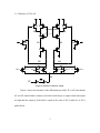

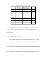
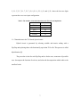
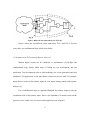
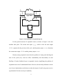
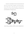
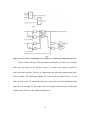
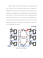


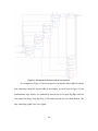
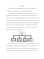


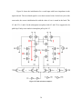

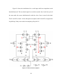

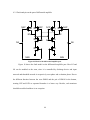

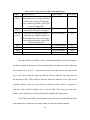
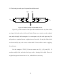
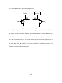

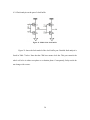
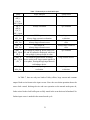
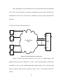


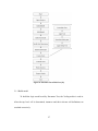

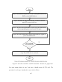
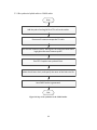


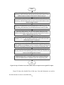


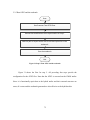
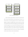


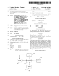


![[Unlocked] SC-2042](http://vs1.manualzilla.com/store/data/005660029_1-1367986a5e7a7fe673239a9957384234-150x150.png)