1
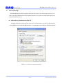
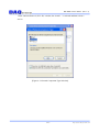
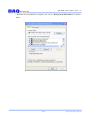
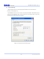
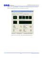
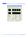
NET-FRM01 Users Manual (Rev 1.2) NET-FRM01 User’s Manual Windows, Windows2000, Windows NT and Windows XP are trademarks of Microsoft. We acknowledge that the trademarks or service names of all other organizations mentioned in this document as their own property. Information furnished by DAQ system is believed to be accurate and reliable. However, no responsibility is assumed by DAQ system for its use, nor for any infringements of patents or other rights of third parties which may result from its use. No license is granted by implication or otherwise under any patent or copyrights of DAQ system. The information in this document is subject to change without notice and no part of this document may be copied or reproduced without the prior written consent. Copyrights 2005 DAQ system, All rights reserved. -1- http://www.daqsystem.com NET-FRM01 Users Manual (Rev 1.2) -- Contents -1. Introduction 2. NET-FRM01 Function 2.1 Block Diagram 2.2 Camera Link 2.3 Camera Link and Connector 2.4 Camera Link and NET-FRM01 3. NET-FRM01 Board Description 3.1 NET-FRM01 Layout 3.2 Functional Blocks 3.3 Connector Pin-out 3.3.1 REF1(RJ45) Connector 3.3.2 J1(MDR26) Connector 3.3.3 J3 Connecter (3Pin Header, 2.54mm) 3.3.4 J7 Connector 3.3.1 SW1 Switch 4. Driver & Network IP Setup 4.1 Filter Driver Installation for Win XP 4.2 Filter Driver Installation for Win 7 4.3 Network IP Setup 5. Sample Program 5.1 Image Frame Function 5.2 UART/Status Function Appendix A.1 General Specification A.2 Physical Dimension Reference -2- http://www.daqsystem.com NET-FRM01 Users Manual (Rev 1.2) 1. Introduction The NET-FRM01 is a board having the function of processing the frame data received from Camera-link camera and transmitting the image frame data to PC through 10/100/1000Mbps Ethenrnet Network. The operation of the board is controlled by program API, figure [1-1] shows connection of the system (usually PC). DAQ system provides a sample program to use the board briefly so you can test the API pr ovided insource form, so the user can be used to modify. Please refer to Chapter 5 for a deta iled description of this sample program. Camera-Link Camera Base NET-FRM01 HUB or Router www.daqsystem.com DAQ system MDR-26 Camera-Link Connecter [Figure 1-1. NET-FRM01 Board Usage] As shown in Figure [1-1], the NET-FRM01 receives Image Frame from camera via Camera-Link Standard Interface. And, the Image Frame data transmit to the PC through the network device like as HUB or Router. -3- http://www.daqsystem.com NET-FRM01 Users Manual (Rev 1.2) [NET-FRM01 Features] Supports Base Configuration Camera Link Camera Fully Plug-and-Play 24/16/8bit Frame Data Acquisition Supports 10/100/1000Mbps (RJ-45 Ethernet Connector) Selectable Board Network Information (IP, etc.) Supports Fixed IP UART(Data 8 bits, 1bit start, 1 stop, No parity, 9600/19200/38400/57600/115200bps) Rx/Tx O.S : Windows XP SP1over, Windows 7 Convenient Windows Application Programming Interface(DLL) [Application] Image Acquisition (Pattern, Particle etc.) Inspection Equipment (Sensor, Semiconductor, Device etc.) Security Solution Medical Image Capture -4- http://www.daqsystem.com NET-FRM01 Users Manual (Rev 1.2) 2. NET-FRM01 Functions 2.1 Block Diagram As shown in the following figure, main control of the board is performed in FPGA Core Logic. The primary functions are receiving the frame data and are transmitting/receiving the UART data. NET-FRM01 DDR2 #1 DDR2 #2 RX0+/M D R I 26 10/100/1000Mbps Ethernet RX1+/RX2+/Camera Control+/Clock Rx/Tx Camera Link Receiver FPGA Core Logic Tranceiver [Figure 2-1. NET-FRM01 Block Diagram] Programming FPGA Core Logic is performed via the JTAG interface. The logic program of the FPGA is saved in a flash ROM, it is located on the board and loaded at the power-up time. -5- http://www.daqsystem.com NET-FRM01 Users Manual (Rev 1.2) 2.2 Camera Link Camera Link is a communication interface for use in a vision application development. In the past, the camera manufacturer and Frame Grabber manufacturers use their own standard connectors and cables. This has caused a lot of confusion and increased costs to users. In order to eliminate this confusion and increase the data rate and data transmission trouble, the specifications of Camera Link interface have been made to the regulations of cable or connector assembly specifications, transfer speed, transfer method at the meeting of camera makers and Frame grabber manufacturers. Currently, many digital video solution use the LVDS (Low Voltage Differential Signal) communication as defined RS-644. LVDS is a way to improve the existing RS-422 that had intractable cable and transmission speed limit. RS-644 LVDS was the Camera Link standard. The LVDS can be transferred the data at high speed using low voltage swing differential signal Differential Signal. This is compared with the existing single-ended signal (Single-ended Signal) using one of the lines, the differential signal transmits the signal using two complementary lines. Such a transfer is characterized by excellent noise immunity, low power consumption, large inphase voltage transmission to refer only to the data transfer on the ground, however Single-ended system is impossible. Camera Link has multiple configuration with depending on the amount of data to be transferred. Base Configuration consists of 28 bits, including a 24-bit pixel data and 3-bit video sync signal lines of the Data Valid, Frame Line Valid, Line Valid, one reserved signal line, and can transmit 2.04Gbit / s (256MB / s). Medium Configuration can be transmitted the 48bit video signal to 4.08Gbit/s(510Mb/s), Full Configuration can be transmitted the 64bit video signal to 5.44Gbit/s(680MB/s). Camera Link requires two cables to transfer more than Medium Specifications. Transmitter part is converted to LVDS data stem’s 4/8/12 from 28/48/64 bit CMOS / TTL data only. Converted signal is transmitted to MDR Cable in accordance with the Transmit Clock signal, the opposite Receiver will be converted into parallel LVDS data of 28/48/64 bits of CMOS / TTL according to the Receive Clock signal from 4/8/12 LVDS data. This Channel Link technology can immediately take advantage of the low cost chip-set because easy to learn and easy to transplant. Camera Link Interface includes Base Configuration, Medium Configuration, Full Configuration. Base Configuration is used 4 RS-644 LVDS pairs for controlling the Transmitter/Receiver and Camera like Figure 2-2, is used for communication between the camera and the frame grabber. Transferred the data from serial 26-Pin MDR Cable, is used to change 28-bit parallel image data at -6- http://www.daqsystem.com NET-FRM01 Users Manual (Rev 1.2) the Receiver part of Frame Grabber. [Figure 2-2. Base Camera Link Block Diagram] -7- http://www.daqsystem.com NET-FRM01 Users Manual (Rev 1.2) 2.3 Camera Link Cable & Connecter The connection between the camera link cameras and NET-FRM01 board uses the 26 Pin Mini MDR (Mini D Ribbon) cable. Camera Link cable consists of twin-axial shielded cable and 2 Mini MDR 26-male plug. The bottom of Figure 2-4 Camera Link cable is typically used. 26-Pin Mini MDR Connecter is located at the end of the cable as like Figure 2-5, Figure 2-6 is 26Pin Mini MDR Connecter, placed at the Camera or Frame Grabber. As shown in the figure, Pin numbers are cross-linked to each other, Transmitter and Receiver of Camera and Frame Grabber signals are connected cross each other. [Figure 2-3. MDR-26 Camera Link Straight Cable] [Figure 2-4. MDR-26 Cable (Male) Pin Map] [Figure 2-5. MDR-26 Connecter (Female) Pin Map] -8- http://www.daqsystem.com NET-FRM01 Users Manual (Rev 1.2) 2.4 Camera Link and NET-FRM01 NET-FRM01 supports Camera Link Base/Medium/Full Configuration. Base Configuration, 24 data bits and four enable signals Frame Valid, Line Valid, Data Valid and a spare, including 28-bit parallel signals serialized four LVDS signal lines and one LVDS signal line to fit the camera and synchronous LVDS signal lines including four CC (Camera Control) signal and full 11 includes two asynchronous serial communication to communicate with the camera LVDS lines, is transmitted through one MDR cable. In order to use the MDR Medium / Full Configuration is used other cable and has a total 64bit wide video path. The transmitted signal is parallelized to 64-bit parallel image signal and Frame Valid, Line Valid, Data Valid, and a spare for each specification from 12 image LVDS serial signal through channel link chip of NET-FRM01. CCx+ Camera Control CCx- Above picture is a Camera Control output circuit from USB3-FRM13 board to Camera for the specific control of the Camera-link Cable. The NET-FRM01 board has four differential digital outputs. Each output is mapped by Digital output. Below picture[Figure 2-6] display that each bit position set. -9- http://www.daqsystem.com NET-FRM01 Users Manual (Rev 1.2) CC1+ CC_D0 CC1CC2+ CC_D1 CC2CC3+ CC_D2 CC3CC4+ CC_D3 CC4[Figure 2-6. Camera Control LVDS Digital Output Circuit] The serial input signal through the Camera-link cable is used for general input circuit from NETFRM01 board. [Figure 2-7. Serial Communication LVDS Digital Output Circuit] -10- http://www.daqsystem.com NET-FRM01 Users Manual (Rev 1.2) 3. NET-FRM01 Board Description In this chapter, the primary functions of the board are described briefly. For more information, refer to the device specification. 3.1 NET-FRM01 Layout NET-FRM01 Board U2 U1 D1 REF1 789 123 A C E G J L N R U3 DAQ REF2 123 A C E G J L N R www.daqsystem.com 789 REF4 system U4 REF5 U5 REF6 J2 D2 D3 D4 D5 D6 U7 U6 J4 J3 J1 SW1 J5 U9 Y1 U8 J7 SW2 [Figure 3-1. NET-FRM01 Layout] The board has 6 LEDs to indicate the operation status. D1 : turns on when power(3.3V) is applied to the board.. D2 ~ D5 : turns on and off when the network configuration is complete. D6 : turns on when power is applied to the board and the initialization ends up. -11- http://www.daqsystem.com NET-FRM01 Users Manual (Rev 1.2) 3.2 Functional Blocks (1) FPGA : U5 All of the functions are controlled by the logic program of the FPGA. (2) DDR Memory : REF1, REF2 After save the data in a frame unit, transfer to PC through FPGA. (3) Oscillator : REF4, Y1 10/100/1000Mbps Ethernet Transceiver provides a 25MHz clock. 50MHz is supplied to the FPGA. (4) Ethernet Module : REF5 10/100/1000Mbps Ethernet Module (RJ-45 Connector) (5) 10/100/1000Mbps Ethernet Transceiver : REF6 The Ethernet Physical Layer of 1000BASE-T is executed. (6) Regulator : U1, U2, The Regulator is for supplying the power (3.3V) to the board. (7) LVDS Channel : U3 It is protected a circuit that the interface of high voltage higher than 3.3V CMOS Logic is exchanged to normal 3.3V Logic Level. -12- http://www.daqsystem.com NET-FRM01 Users Manual (Rev 1.2) 3.3 Connector Pin-out This chapter will be described about the connector and Jumper that NET-FRM01 used. The NET-FRM01 board is equipped with RJ-45 connector REF1 for Network connection and J1 connector for external Image Frame connection(Camera Link Signals). 3.3.1 REF1(RJ-45) Connector When viewed from the front of the cable is connected to PIN of RJ-45 connectors, it is as [Figure 3-2]. 12 3 4 5 6 7 8 [Figure 3-2. RJ-45 Connector(Front View)] [Table 1. RJ-45 Connector] Pin 1000BASE-T Signal ID 1 DA+ 2 DA- 3 DB+ 4 DC+ 5 DC- 6 DB- 7 DD+ 8 DD- Remark -13- http://www.daqsystem.com NET-FRM01 Users Manual (Rev 1.2) 3.3.2 J1(MDR26) Connector Figure [3-3] shows the board’s J4 connector pin-map. All of the pin functions are based on the Camera link standard, so please refer to the Camera link standard document for more description and information. Frame Grabber Inner shield 26 13 Inner shield X0- 25 12 X0+ X1- 24 11 X1+ X2- 23 10 X2+ Xclk- 22 9 Xclk+ X3- 21 8 X3+ SerTC+ 20 7 SerTC- SerTFG- 19 6 SerTFG+ CC1- 18 5 CC1+ 17 4 CC2- 16 3 CC3+ 15 2 CC4- 14 1 Inner shield CC2+ CC3CC4+ Inner shield [Figure 3-3. NET-FRM01 J1 Connector Pin-out] -14- http://www.daqsystem.com NET-FRM01 Users Manual (Rev 1.2) [Table 2. J1 Connector Description] Pin Signal Name 1 Inner Shield 2 CC4- Camera Control output 4- 3 CC3+ Camera Control output 3+ 4 CC2-- Camera Control output 2- 5 CC1+ Camera Control output 1+ 6 SerTFG+ Serial to Frame grabber + 7 SerTC- 8 X3+ Camera link LVDS receive data3 + 9 Xclk+ Camera link LVDS receive clock + 10 X2+ Camera link LVDS receive data2 + 11 X1+ Camera link LVDS receive data1 + 12 X0+ Camera link LVDS receive data0 + 13 Inner Shield 14 Inner Shield 15 CC4+ Camera Control output 4+ 16 CC3- Camera Control output 3- 17 CC2+ Camera Control output 2+ 18 CC1- Camera Control output 1- 19 SerTFG- Serial to Frame grabber- 20 SerTC+ Serial to Camera+ 21 X3- Camera link LVDS receive data3- 22 Xclk- Camera link LVDS receive clock- 23 X2- Camera link LVDS receive data2- 24 X1- Camera link LVDS receive data1- 25 X0- Camera link LVDS receive data0- 26 Inner Shield (Note) Description Remark Cable shield Serial to Camera- For more information, refer to Camera Link Standard Specification. -15- http://www.daqsystem.com NET-FRM01 Users Manual (Rev 1.2) 3.3.3 J3 Connector (3Pin Header, 2.54mm) It is an external RS-232 Debug Port. 1 2 3 [Figure 2-4. J3 Connector (Top View)] [Table 3. J3 PIN-OUT Description] No. Name Description 1 U_SPI_MISO Tx (Transceiver Data) 2 U_SPI_MOSI Rx (Receiver Data) 3 GND Ground 3.3.4 J7 Connector It is an external 12V DC Jack Power Connector of DC-005 (2.0) standard. 12V 1.0A [Figure 2-5. Rated Output] 3.3.5 SW1 Switch Board On/Off Switch. VCC12_WALL SW_T_SPOT GND 1 2 12.0V 3 [Figure 2-6. SW1 Switch] -16- http://www.daqsystem.com NET-FRM01 Users Manual (Rev 1.2) 4. Network Setup The NET-FRM01 don’t need a separate device driver because it uses for network. However, it is used by specifying IP(Internet Protocol) address identifier. It is possible to install and use the service on the network Filter Driver. 4.1 Filter Driver Installation for Win XP Installed a filter driver can reduce the PC resources. The procedure is as follows. "My Network Places local area connection properties" is selected, this comes under the network properties. [Figure 4-1. Network Connection Property] -17- http://www.daqsystem.com NET-FRM01 Users Manual (Rev 1.2) In the “Internet Protocol (TCP / IP)” window, the "install ..." is selected and then selects a service. [Figure 4-2. Network Component Type Selection] -18- http://www.daqsystem.com NET-FRM01 Users Manual (Rev 1.2) Select a "Have Disk…" in the "Select Network Service" and click "Browse (B) ...". You can find a “netsf.ini” file from the provided CD-ROM, and then click OK. -19- http://www.daqsystem.com NET-FRM01 Users Manual (Rev 1.2) “Select Network Service”, and then click the [OK], and requires a check of compatibility. -20- http://www.daqsystem.com NET-FRM01 Users Manual (Rev 1.2) When the driver installation is complete, you can see "DAQ System Filter Driver" as shown below. -21- http://www.daqsystem.com NET-FRM01 Users Manual (Rev 1.2) 4.2 Filter Driver Installation for Win 7 In the case of Win7, you run the program with administrator privileges to depending on the setting of the operating system. You can prevent the execution of the block of DAQ system against firewall program. If you cannot share a computer, and can use a computer in the office, please ask them to contact the administrator user of your PC, you are given administrator rights to your user account. The rest of the process is the same as Win XP. If FrameTest.exe executable file doesn’t not perform as firewall, Press the “Control Panel System and Security Windows Firewall Allows the Program through Window Firewall”. You have to permit as shown below “frametest.exe Home/Company(Private)”. [Figure 4-3. Allows program when shut off the firewall] -22- http://www.daqsystem.com NET-FRM01 Users Manual (Rev 1.2) 4.3 Network IP Setup Before using the board, it uses after specifying the IP address in the “Internet Protocol (TCP/IP)” as shown [Figure 4-1]. The NET-FRM01 board 192.168.33.129 IP is used as the fixed identifier. This identifier does not overlap with the appropriate choice of IP, 255.255.255.0 as the subnet mask set used. The remaining portion of the selection may be omitted. [FIgure 4-4. Internet Protocol(TCP/IP) Property] -23- http://www.daqsystem.com NET-FRM01 Users Manual (Rev 1.2) When you use the NET-FRM01, it is possible not to install the filter driver as section 4.1. However, using the filter driver can be reduced the PC's resources. [Figure 4-5. PC CPU Usage - when did not install the filter driver] -24- http://www.daqsystem.com NET-FRM01 Users Manual (Rev 1.2) [Figure 4-6. PC CPU Usage - When install the filter driver] -25- http://www.daqsystem.com NET-FRM01 Users Manual (Rev 1.2) 5. Sample Program DAQ system provides a sample program to make the user be familiar with the board operation and to make the program development easier. You can find the sample program in the CDROM accompanying with the board. Before using the program, as part of Network Configuration chapter 4 PC Internet TCP / IP address must be set first. [Figure 5-1. When Sample program “FrmTest.exe’ is executed] -26- http://www.daqsystem.com NET-FRM01 Users Manual (Rev 1.2) 5.1 Image Frame Function (1) “Dev. Open” button It starts a selected board device. If it is “0”, it is the normal state. If it is “-1”, the device is not recognized. (2) “Dev. Init” button Press this button to initialize the function of receiving image frame data. It is performed only once after power is applied to the board. (3) Mode Selection It selects a Video Data Mode of 8bit, 16bit, 24bit, 32bit. (4) “Get Res.” button It shows the image resolution. (5) “Start” button It starts the image transfer. It is a Toggle button, press again stop the image transferring. (6) “Once” button When press this button, it displays a freeze-frame. (7) “View” button Start the image transmission. (8) “Data” button Press this button to read the image frame data of the board to your PC(Hex Value). If image frame data is not saved on the board, you must wait until the end of data collection. (9) “Auto” toggle When check this box, it displays a video -27- http://www.daqsystem.com NET-FRM01 Users Manual (Rev 1.2) (10) “Display Skip” toggle When press this button, it displays a freeze-frame. (11) “F/R” Frame rates/sec (12) “Pkt Delay” Selection You can select a next Package Delay 0 ~ 15 after transfer Package. The unit is 5us. (13) “Shift Bits” It is an option for Black/White Camera test, the bits 0-8 of the input frames can be moved to the right. For example, you can view the images(8bit) after shifting 4bit in case of 12bit Black/White camera. 5.2 UART/Status Function (1) “Baud” Selection Select the Baud Rate (9600, 19200, 38400, 57600, 115200 Baud Rate). (2) “Send Serial” button Send the UART data. -28- http://www.daqsystem.com NET-FRM01 Users Manual (Rev 1.2) (3) “Get Serial” button Get the data from UART buffer. (4) ”Auto Get Signal” toggle When check this box, the serial data from Frame Grabber will be displayed in the below box. (5) “Clear Data” button Clear the UART Receiver buffer. (6) “CC Out” button Write CC(Camera Control) Data. (7) “CC Read” button Read CC(Camera Control) Data. . -29- http://www.daqsystem.com NET-FRM01 Users Manual (Rev 1.2) Appendix A.1 General Specification Image Input One Base Camera Link Output 10/100/1000 Mbps Ethernet Interface Serial Interface (Option) 8bit Data, 1 Stop bit, No parity Baud Rates --- 9600, 19200, 38400, 57600, 115200 Power Requirement Voltage : +12V (Max. 1A) Environment Caution) When using internal, Operating Temperature : 0 ℃ ~ 60 ℃ Storage Temperature : -20 ℃ ~ 70 ℃ Relative Humidity : 5% ~ 90%, non-condensing Software OS : 32/64bit Windows XP SP1/Windows 7 SP1 API : Interface with Application through client DLL Sample Software : Test Sample software for evaluat ion -30- http://www.daqsystem.com NET-FRM01 Users Manual (Rev 1.2) A.2 Physical Dimension Dimensions of the board are as follows: 4.5 6.5 3.0 4.5 79.5 47 32 29 21 110 < Top View > 20 13 1.6 5.0 < Right Side View > -31- http://www.daqsystem.com NET-FRM01 Users Manual (Rev 1.2) References 1. AN201 How to build application using API -- DAQ system 2. AN342 NET-FRM01 API ver1.0 -- DAQ system -32- http://www.daqsystem.com