1
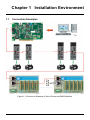
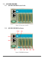
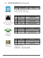
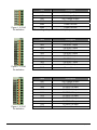
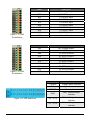
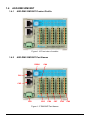
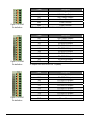
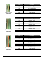
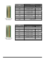
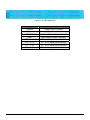
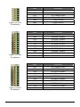
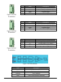
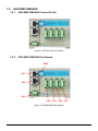
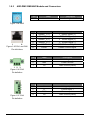
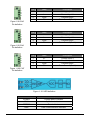
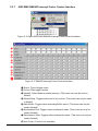
DELTA ELECTRONICS CO., LTD. DMCNET Remote Module Remote Digital I/O Module User Manual Revised: 1.11.1 Revised April, 2012 i About this Manual User Information Please keep this manual in a safe place. This manual is subject to change without notice due to the release of new products, improvements and changes in technologies, and/or modifications to data and forms. This manual may not be copied or reproduced in whole or in part without the express written consent of Delta Electronics Co., Ltd. Trademarks Windows 2000/XP, Visual Studio, Visual C++, and Visual BASIC are all registered trademarks owned by Microsoft. BCB (Borland C++ Builder) is a registered trademark of Borland Corporation. The names of other products are only used for identification purposes. All registered trademarks remain the property of their respective owners. Technical Support and Service If you need any technical support, service, or other information, or should you have any questions in using the products, please visit our website (http://www.delta.com.tw/ia) or contact us directly. We are looking forward to serve your needs and willing to offer our best support and service to you. Our contact details are provided below. Reach us by the following ways. ii ASIA DELTA ELECTRONICS, INC. Taoyuan Plant 1 31-1, XINGBANG ROAD, GUISHAN INDUSTRIAL ZONE, TAOYUAN COUNTY 33370, TAIWAN, R.O.C. TEL: 886-3-362-6301 FAX: 886-3-362-7267 JAPAN DELTA ELECTRONICS (JAPAN), INC. Tokyo Office DELTA SHIBADAIMON BUILDING 2-1-14 SHIBADAIMON, MINATO-KU, TOKYO, 105-0012, JAPAN TEL: 81-3-5733-1111 FAX: 81-3-5733-1211 NORTH/SOUTH AMERICA DELTA PRODUCTS CORPORATION (USA) Raleigh Office P.O. BOX 12173 5101 DAVIS DRIVE, RESEARCH TRIANGLE PARK, NC 27709, U.S.A. TEL: 1-919-767-3813 FAX: 1-919-767-3969 EUROPE DELTRONICS (THE NETHERLANDS) B.V. Eindhoven Office DE WITBOGT 15, 5652 AG EINDHOVEN, THE NETHERLANDS TEL: 31-40-259-2850 FAX: 31-40-259-2851 Revised April, 2012 Table of Contents Chapter 1 Installation Environment----------------------------------------------------------------------------- 1-1 1.1 Connection Examples------------------------------------------------------------------------------ 1-1 1.2 Electrical Specifications --------------------------------------------------------------------------- 1-4 1.3 ASD-DMC-RM32MN ------------------------------------------------------------------------------- 1-6 1.3.1 1.3.2 1.3.3 1.4 1.5 ASD-DMC-RM32NT -------------------------------------------------------------------------------1-10 1.4.1 ASD-DMC-RM32NT Product Profile ----------------------------------------------1-10 1.4.2 1.4.3 ASD-DMC-RM32NT Part Names --------------------------------------------------1-10 ASD-DMC-RM32NT Module and Connectors ----------------------------------1-11 ASD-DMC-RM64MN ------------------------------------------------------------------------------1-14 1.5.1 1.5.2 1.5.3 1.6 ASD-DMC-RM64NT Product Profile ----------------------------------------------1-21 ASD-DMC-RM64NT Part Names --------------------------------------------------1-21 ASD-DMC-RM64NT Module and Connectors ----------------------------------1-22 ASD-DMC-RM04PI --------------------------------------------------------------------------------1-28 1.7.1 1.7.2 1.7.3 1.8 ASD-DMC-RM64MN Product Profile ---------------------------------------------1-14 ASD-DMC-RM64MN Part Names -------------------------------------------------1-14 ASD-DMC-RM64MN Module and Connectors ---------------------------------1-15 ASD-DMC-RM64NT -------------------------------------------------------------------------------1-21 1.6.1 1.6.2 1.6.3 1.7 ASD-DMC-RM32MN Product Profile ---------------------------------------------- 1-6 ASD-DMC-RM32MN Part Names -------------------------------------------------- 1-6 ASD-DMC-RM32MN Module and Connectors ---------------------------------- 1-7 ASD-DMC-RM04PI Product Profile -----------------------------------------------1-28 ASD-DMC-RM04PI Part Names ---------------------------------------------------1-28 ASD-DMC-RM04PI Module and Connectors -----------------------------------1-29 ASD-DMC-RM04DA-------------------------------------------------------------------------------1-35 1.8.1 1.8.2 1.8.3 Revised April, 2012 ASD-DMC-RM04DA Product Profile ----------------------------------------------1-35 ASD-DMC-RM04DA Part Names--------------------------------------------------1-35 ASD-DMC-RM04DA Module and Connectors----------------------------------1-36 iii 1.9 1.10 1.11 ASD-DMC-RM04AD-------------------------------------------------------------------------------1-38 1.9.1 ASD-DMC-RM04AD Product Profile ----------------------------------------------1-38 1.9.2 1.9.3 ASD-DMC-RM04AD Part Names--------------------------------------------------1-38 ASD-DMC-RM04AD Module and Connectors----------------------------------1-39 ASD-DMC-RM32PT -------------------------------------------------------------------------------1-41 1.10.1 ASD-DMC-RM32PT Product Profile ----------------------------------------------1-41 1.10.2 1.10.3 ASD-DMC-RM32PT Part Names --------------------------------------------------1-41 ASD-DMC-RM32PT Module and Connectors ----------------------------------1-42 ASD-DMC-RM64MN1-----------------------------------------------------------------------------1-45 1.11.1 1.11.2 1.11.3 1.12 ASD-DMC-RM64NT1 -----------------------------------------------------------------------------1-49 1.12.1 1.12.2 1.12.3 1.13 ASD-DMC-RM64MN1 Product Profile--------------------------------------------1-45 ASD-DMC-RM64MN1 Part Names------------------------------------------------1-45 ASD-DMC-RM64MN1 Module and Connectors--------------------------------1-46 ASD-DMC-RM64NT1 Product Profile --------------------------------------------1-49 ASD-DMC-RM64NT1 Part Names ------------------------------------------------1-49 ASD-DMC-RM64NT1 Module and Connectors --------------------------------1-50 Wiring Example-------------------------------------------------------------------------------------1-53 1.13.1 1.13.2 1.13.3 1.13.4 1.13.5 1.13.6 1.13.7 1.13.8 1.13.9 Wiring of RM32MN/RM32PT/RM64MN/RM64MN1 Input Points ----------1-53 Wiring of RM32NT/RM32PT/RM64NT/RM64NT1 Output Points ----------1-53 Wiring of RM04PI Input point (MEL, PEL, ORG, SLD) -----------------------1-54 Wiring of RM04PI Output point (CW, CCW, D01, D02) ----------------------1-54 Connecting RM04PI to Stepping Motor Drive ----------------------------------1-55 Connecting RM04PI to Encoder ---------------------------------------------------1-57 Connecting RM64MN to MPG ------------------------------------------------------1-57 Wiring Diagram for RM04DA Output Point --------------------------------------1-58 Wiring Diagram for RM04AD Input Point ----------------------------------------1-58 Chapter 2 Using EzDMC ------------------------------------------------------------------------------------------ 2-1 2.1 Launching the Program---------------------------------------------------------------------------- 2-1 2.2 Connecting to Remote Module ------------------------------------------------------------------ 2-2 2.3 Remote Module Interface ------------------------------------------------------------------------- 2-3 2.3.1 2.3.2 2.3.3 2.3.4 iv ASD-DMC-RM32MN ------------------------------------------------------------------- 2-3 ASD-DMC-RM32NT ------------------------------------------------------------------- 2-3 ASD-DMC-RM64MN(1) --------------------------------------------------------------- 2-4 ASD-DMC-RM64NT(1) ---------------------------------------------------------------- 2-6 Revised April, 2012 2.3.5 2.3.6 2.3.7 2.3.8 2.3.9 2.3.10 2.3.11 ASD-DMC-RM04PI (MODE 1) ------------------------------------------------------ 2-7 ASD-DMC-RM04PI (MODE 2) -----------------------------------------------------2-10 ASD-DMC-RM04PI Interrupt Factor Control Interface------------------------2-13 ASD-DMC-RM04PI Slave Encryption Control Interface----------------------2-14 ASD-DMC-RM04DA ------------------------------------------------------------------2-16 ASD-DMC-RM04AD ------------------------------------------------------------------2-18 ASD-DMC-RM32PT-------------------------------------------------------------------2-20 Appendix A ----------------------------------------------------------------------------------------------------------- A-1 FAQ ----------------------------------------------------------------------------------------------------------- A-1 Revised April, 2012 v Chapter 1 Installation Environment Connection Examples Terminal Resistor 1.1 Figure 1.1 Connection Example of Servo Drives and RM32 Modules Revised April, 2012 1-1 Terminal Resistor Figure 1.2 Connection Example of Servo Drives and RM64 Modules 1-2 Revised April, 2012 Terminal Resistor Figure 1.3 Connection Example of Servo Drives and RM04PI Modules Revised April, 2012 1-3 1.2 Electrical Specifications General RM32 Module (MN/NT/PT) Dimensions: 100mm x 75mm x 43mm RM64 Module (MN/NT) Dimensions: 168mm x 75mm x 43mm RM04PI Module Dimensions: 168mm x 75mm x 40mm RM04DA Module Dimensions: 100mm x 75mm x 43mm RM04AD Module Dimensions: 100mm x 75mm x 43mm Power Supply Voltage: 24 VDC(15% ~ 20%) ESD: 8KV Air Discharge EFT: Power Line-2KV Digital I/O 1KV RS: 80MHz ~ 1GHz, 10V/m Operating Temperature: 0 oC ~ 50 oC Digital Signal Input Point (RM32MN & RM64MN & RM32PT & RM64MN1) Input Circuit Type: Single-end Common Input: Input Signal Type: SINK / SOURCE Input Signal Voltage: 24VDC (5mA) Response Time: 0 ~ 3ms Adjustable Trigger Level (OFF->ON): >16.5VDC Trigger Level (ON->OFF): <8VDC Pulse Interface Input Port (RM04PI Input) Input Circuit Type: Single-end Common Input: Input Signal Type: SINK / SOURCE Input Signal Voltage(Sensor) : 24VDC(5mA) Response Time: 1ms Trigger Level(OFF->ON): >16.5VDC Trigger Level (ON->OFF): <8VDC Input signal is 5VDC and SINK type only: Maximum Switching (Operating) Frequency: QA, QB, QZ: 200KHz (5mA/1 point) DI1, DI2: 1KHz (5mA/1 point) 1-4 Digital Signal Output Point (RM32NT & RM64NT & RM32PT & RM64NT1) Output Circuit Type: Transistor Output Signal Type: SINK Maximum Switching (Operating) Frequency: 1KHz Current Specifications: 0.1A/1 point Voltage Specifications: 24VDC Response Time(OFF->ON): 20us Response Time(ON->OFF): 30us Pulse Interface Output Port (RM04PI Output) Output Circuit Type: Transistor Output Signal Type: SINK Output Signal Voltage: 5~24VDC (30mA/1 point) Maximum Switching (Operating) Frequency: CW, CCW:200KHz (30mA/1 point) DO1, DO2:1KHz (30mA/1 point) Revised April, 2012 Digital to Analog Output Point (RM04DA) Channel: 4 channels /unit Voltage Output Range: -10~10 V / -5~5V / 0~10V / 0~5V Current Output Range: 0~24mA / 0~20mA / 4~20mA Excess Limit (Voltage): 10% Maximum Output Current (Voltage): 24mA Allowable Load Resistance (Current):0~500Ω Digital Data Range: 0~4096 Resolution: 16 bits DC Output Resistance: 0.3Ω Response Time: 1ms Digital Data Format: 16 valid data bits Isolation method: Internal circuit and analog output are isolated using an optical coupler. Protection: Voltage output circuit has short-circuit protection, but extended time short-circuit may damage the internal circuit and open path to current output. Digital to Analog Input Point (RM04AD) Channel: 4 channels /unit Voltage Analog Input Range: -10~10V / -5~5V / 0~10V / 0~5V Current Analog Input Range: 0~20mA Digital Conversion Range: 0~65535 Resolution: 16bits Voltage Input Resistance: 140KΩ Current Input Resistance: 249Ω General Precision: Within ±0.5% (25°C, 77°F) at full scale. Within ±1% (0~55°C, 32~131°F) at full scale Response Time: Minimum of 1ms, maximum of 3ms x number of channels Isolation method: Internal circuit and analog input isolated using optical coupler Current Absolute Input Range:-15 ~ 15 Voltage Absolute Input Range: 32mA Digital Data Format: 16 valid data bits Averaging function: Modes 2.4.8.16.32 provided Revised April, 2012 1-5 1.3 ASD-DMC-RM32MN 1.3.1 ASD-DMC-RM32MN Product Profile Figure 1.4 Front view of module 1.3.2 ASD-DMC-RM32MN Part Names RSW1 CN4 CN1 CN2 CN3 CN5 CN6 CN7 CN8 CN9 Figure 1.5 RM32MN Part Names 1-6 Revised April, 2012 1.3.3 ASD-DMC-RM32MN Module and Connectors Figure 1.6 RSW1 1 8 Figure 1.7 CN1 and CN2 Pin definitions Pin Label Description 1~ 12 Node Number Node ID ※ Invalid when dial is turned to 0, D ~ F ※ Each module takes up one Node ID Pin Label Description 1 RS485T_1 (+) 1st RS485 Signal (+) 2 RS485T_1 (-) 1st RS485 Signal (-) 3 RS485T_2 (+) 2nd RS485 Signal (+) 6 RS485T_2 (-) 2nd RS485 Signal (-) 7 EGND RS485 Ground Signal 8 EGND RS485 Ground Signal Pin Label Description 3 E24V 24V Voltage Input 2 GND Power Ground 1 FG Case Ground (Earth) Pin Label Description 3 E24V 24V Voltage Output 2 COM Common Input Signal 1 GND Power Ground 1 2 3 Figure 1.8 CN3 Pin definition Figure 1.9 CN4 Pin definition Revised April, 2012 ※ This connector is used with the Input signal common point for Pull high or Pull low ※ COM to 24V → Low active (Pull high) ※ COM to GND → High active (Pull low) 1-7 Figure 1.10 CN5 Pin definition Figure 1.11 CN6 Pin definition Figure 1.12 CN7 Pin definition 1-8 Label Description 24V 24V Voltage Output 24V 24V Voltage Output 24V 24V Voltage Output GND Power Ground GND Power Ground GND Power Ground ※ Total voltage Output at 24V is 1.5A (Max) Label Description 24V 24V Voltage Output X00 P0 GPIO 1 Input X01 P0 GPIO 2 Input X02 P0 GPIO 3 Input X03 P0 GPIO 4 Input X04 P0 GPIO 5 Input X05 P0 GPIO 6 Input X06 P0 GPIO 7 Input X07 P0 GPIO 8 Input GND Power Ground Label Description 24V 24V Voltage Output X08 P0 GPIO 9 Input X09 P0 GPIO 10 Input X10 P0 GPIO 11 Input X11 P0 GPIO 12 Input X12 P0 GPIO 13 Input X13 P0 GPIO 14 Input X14 P0 GPIO 15 Input X15 P0 GPIO 16 Input GND Power Ground Revised April, 2012 Figure 1.13 CN8 Pin definition Figure 1.14 CN9 Pin definition Figure 1.15 LED definitions Revised April, 2012 Label Description 24V 24V Voltage Output X00 P1 GPIO 1 Input X01 P1 GPIO 2 Input X02 P1 GPIO 3 Input X03 P1 GPIO 4 Input X04 P1 GPIO 5 Input X05 P1 GPIO 6 Input X06 P1 GPIO 7 Input X07 P1 GPIO 8 Input GND Power Ground Label Description 24V 24V Voltage Output X08 P1 GPIO 9 Input X09 P1 GPIO 10 Input X10 P1 GPIO 11 Input X11 P1 GPIO 12 Input X12 P1 GPIO 13 Input X13 P1 GPIO 14 Input X14 P1 GPIO 15 Input X15 P1 GPIO 16 Input GND Power Ground Label Description POWER Voltage status indicator RUN Operation indicator ERROR Error indicator DMC DMC communication indicator P0 0~15 P0 0~15 signal Input indicator P1 0~15 P1 0~15 signal Input indicator 1-9 1.4 ASD-DMC-RM32NT 1.4.1 ASD-DMC-RM32NT Product Profile Figure 1.16 Front view of module 1.4.2 ASD-DMC-RM32NT Part Names RSW1 CN4 CN1 CN2 CN3 CN5 CN6 CN7 CN8 CN9 Figure 1.17 RM32NT Part Names 1-10 Revised April, 2012 1.4.3 ASD-DMC-RM32NT Module and Connectors Figure 1.18 RSW1 1 8 Figure 1.19 CN1 and CN2 Pin definitions 1 2 3 Figure 1.20 CN3 Pin definition Figure 1.21 CN4 Pin definition Revised April, 2012 Pin Label Description 1~9 A~F Node Number Node ID ※ Invalid when dial is turned to 0, D ~ F ※ Each module takes up one Node ID Pin Label Description 1 RS485T_1 (+) 1st RS485 Signal (+) 2 RS485T_1 (-) 1st RS485 Signal (-) 3 RS485T_2 (+) 2nd RS485 Signal (+) 6 RS485T_2 (-) 2nd RS485 Signal (-) 7 EGND RS485 Ground Signal 8 EGND RS485 Ground Signal Pin Label Description 3 E24V 24V Voltage Input 2 GND Power Ground 1 FG Case Ground (Earth) Label Description 24V 24V Voltage Output N/A Wire to wire connector GND Power Ground 1-11 Figure 1.22 CN5 Pin definition Figure 1.23 CN6 Pin definition Figure 1.24 CN7 Pin definition 1-12 Label Description 24V 24V Voltage Output 24V 24V Voltage Output 24V 24V Voltage Output GND Power Ground GND Power Ground GND Power Ground ※ Total voltage Output at 24V is 1.5A (Max) Label Description 24V 24V Voltage Output Y00 P0 GPIO 1 Output Y01 P0 GPIO 2 Output Y02 P0 GPIO 3 Output Y03 P0 GPIO 4 Output Y04 P0 GPIO 5 Output Y05 P0 GPIO 6 Output Y06 P0 GPIO 7 Output Y07 P0 GPIO 8 Output GND Power Ground ※ Output from one GPIO is 0.1 A(Max) Label Description 24V 24V Voltage Output Y08 P0 GPIO 9 Output Y09 P0 GPIO 10 Output Y10 P0 GPIO 11 Output Y11 P0 GPIO 12 Output Y12 P0 GPIO 13 Output Y13 P0 GPIO 14 Output Y14 P0 GPIO 15 Output Y15 P0 GPIO 16 Output GND Power Ground Revised April, 2012 Figure 1.25 CN8 Pin definition Figure 1.26 CN9 Pin definition Figure 1.27 LED definition Revised April, 2012 Label Description 24V 24V Voltage Output Y00 P1 GPIO 1 Output Y01 P1 GPIO 2 Input Y02 P1 GPIO 3 Output Y03 P1 GPIO 4 Output Y04 P1 GPIO 5 Output Y05 P1 GPIO 6 Output Y06 P1 GPIO 7 Output Y07 P1 GPIO 8 Output GND Power Ground Label Description 24V 24V Voltage Output Y08 P1 GPIO 9 Output Y09 P1 GPIO 10 Output Y10 P1 GPIO 11 Output Y11 P1 GPIO 12 Output Y12 P1 GPIO 13 Output Y13 P1 GPIO 14 Output Y14 P1 GPIO 15 Output Y15 P1 GPIO 16 Output GND Power Ground Label Description POWER Voltage status indicator RUN Operation indicator ERROR Error indicator DMC DMC communication indicator P0 0~15 P0 0~15 signal Output indicator P1 0~15 P1 0~15 signal Output indicator 1-13 1.5 ASD-DMC-RM64MN 1.5.1 ASD-DMC-RM64MN Product Profile Figure 1.28 Front view of module 1.5.2 ASD-DMC-RM64MN Part Names RSW1 CN4 CN10 CN1 CN2 CN3 CN5 CN6 CN7 CN8 CN9 CN11 CN12 CN13 CN14 CN15 Figure 1.29 RM64MN Part Names 1-14 Revised April, 2012 1.5.3 ASD-DMC-RM64MN Module and Connectors Figure 1.30 RSW1 1 8 Figure 1.31 CN1 and CN2 Pin definitions Pin Label Description 1~9 A~F Node Number Node ID ※ Invalid when dial is turned to 0, D ~ F ※ Each module takes up one Node ID Pin Label Description 1 RS485T_1 (+) 1st RS485 Signal (+) 2 RS485T_1 (-) 1st RS485 Signal (-) 3 RS485T_2 (+) 2nd RS485 Signal (+) 6 RS485T_2 (-) 2nd RS485 Signal (-) 7 GND RS485 Ground Signal 8 GND RS485 Ground Signal Pin Label Description 1 FG Case Ground (Earth) 2 GND Power Ground 3 24V 24V Voltage Input 1 2 3 Figure 1.32 CN3 Pin definition Figure 1.33 CN4 Pin definition Revised April, 2012 Label Description 24V 24V Voltage Output COM Common Input Signal GND Power Ground ※ This connector is used with the Input signal common point for Pull high or Pull low ※ COM to 24V → Low active (Pull high) ※ COM to GND → High active (Pull low) ※ Total Input voltage is 3.0A (Max) 1-15 Figure 1.34 CN5 Pin definition Figure 1.35 CN6 Pin definition Figure 1.36 CN7 Pin definition 1-16 Label Description 24V 24V Voltage Output 24V 24V Voltage Output 24V 24V Voltage Output GND Power Ground GND Power Ground GND Power Ground Total voltage Output at 24V is 1.5A (Max) Label Description 24V 24V Voltage Output X00 P0 GPIO 1 Input X01 P0 GPIO 2 Input X02 P0 GPIO 3 Input X03 P0 GPIO 4 Input X04 P0 GPIO 5 Input X05 P0 GPIO 6 Input X06 P0 GPIO 7 Input X07 P0 GPIO 8 Input GND Power Ground Label Description 24V 24V Voltage Output X08 P0 GPIO 9 Input X09 P0 GPIO 10 Input X10 P0 GPIO 11 Input X11 P0 GPIO 12 Input X12 P0 GPIO 13 Input X13 P0 GPIO 14 Input X14 P0 GPIO 15 Input X15 P0 GPIO 16 Input GND Power Ground Revised April, 2012 Figure 1.37 CN8 Pin definition Figure 1.38 CN9 Pin definition Figure 1.39 CN10 Pin definition Revised April, 2012 Label Description 24V 24V Voltage Output X00 P1 GPIO 1 Input X01 P1 GPIO 2 Input X02 P1 GPIO 3 Input X03 P1 GPIO 4 Input X04 P1 GPIO 5 Input X05 P1 GPIO 6 Input X06 P1 GPIO 7 Input X07 P1 GPIO 8 Input GND Power Ground Label Description 24V 24V Voltage Output X08 P1 GPIO 9 Input X09 P1 GPIO 10 Input X10 P1 GPIO 11 Input X11 P1 GPIO 12 Input X12 P1 GPIO 13 Input X13 P1 GPIO 14 Input X14 P1 GPIO 15 Input X15 P1 GPIO 16 Input GND Power Ground Label Description 24V 24V Voltage Output COM Common Input Signal GND Power Ground 1-17 Figure 1.40 CN11 Pin definition Figure 1.41 CN12 Pin definition Figure 1.42 CN13 Pin definition 1-18 Label Description 24V 24V Voltage Output 24V 24V Voltage Output 24V 24V Voltage Output GND Power Ground GND Power Ground GND Power Ground Total voltage Output at 24V is 1.5A (Max) Label Description 24V 24V Voltage Output X00 P2 GPIO 1 Input X01 P2 GPIO 2 Input X02 P2 GPIO 3 Input X03 P2 GPIO 4 Input X04 P2 GPIO 5 Input X05 P2 GPIO 6 Input X06 P2 GPIO 7 Input X07 P2 GPIO 8 Input GND Power Ground ※ When P3H/P3L (GPIO 3) is set to MPG mode, Pin 9 (P2 X00) and Pin 8 (P2 X01) cannot be used. Label Description 24V 24V Voltage Output X08 P2 GPIO 9 Input X09 P2 GPIO 10 Input X10 P2 GPIO 11 Input X11 P2 GPIO 12 Input X12 P2 GPIO 13 Input X13 P2 GPIO 14 Input X14 P2 GPIO 15 Input X15 P2 GPIO 16 Input GND Power Ground Revised April, 2012 Label 24V Figure 1.43 CN14 Pin definition MPG mode 24V Voltage Output P3 GPIO 1 Input X X01 P3 GPIO 2 Input Y X02 P3 GPIO 3 Input Z X03 P3 GPIO 4 Input U X04 P3 GPIO 5 Input x1 X05 P3 GPIO 6 Input x10 X06 P3 GPIO 7 Input x100 X07 P3 GPIO 8 Input EN GND E24V Revised April, 2012 GPIO mode X00 Label Figure 1.44 CN15 Pin definition Description Power Ground Description GPIO mode MPG mode 24V Voltage Output X08 P3 GPIO 9 Input PA X09 P3 GPIO 10 Input PB X10 P3 GPIO 11 Input J1+ X11 P3 GPIO 12 Input J1- X12 P3 GPIO 13 Input J2+ X13 P3 GPIO 14 Input J2- X14 P3 GPIO 15 Input J3+ X15 P3 GPIO 16 Input J3- GND Power Ground 1-19 Figure 1.45 LED definition 1-20 Label Description POWER Voltage status indicator RUN Operation indicator ERROR Error indicator DMC DMC communication indicator P0 0~15 P0 0~15 signal Input indicator P1 0~15 P1 0~15 signal Input indicator P2 0~15 P2 0~15 signal Input indicator P3 0~15 P3 0~15 signal Input indicator Revised April, 2012 1.6 ASD-DMC-RM64NT 1.6.1 ASD-DMC-RM64NT Product Profile Figure 1.46 Front view of module 1.6.2 ASD-DMC-RM64NT Part Names RSW1 CN4 CN10 CN1 CN2 CN3 CN5 CN6 CN7 CN8 CN9 CN11 CN12 CN13 CN14 CN15 Figure 1.47 RM64NT Part Names Revised April, 2012 1-21 1.6.3 ASD-DMC-RM64NT Module and Connectors Figure 1.48 RSW1 Pin Label Description 0~9 A~F Node Number Node ID ※ Invalid when dial is turned to 0, D ~ F ※ Each module takes up one Node ID Label Description RS485T_1 (+) 1st RS485 Signal (+) RS485T_1 (-) 1st RS485 Signal (-) RS485T_2 (+) 2nd RS485 Signal (+) RS485T_2 (-) 2nd RS485 Signal (-) GND RS485 Ground Signal GND RS485 Ground Signal 1 8 Figure 1.49 CN1 and CN2 Pin definitions 1 2 3 Figure 1.50 N3 Pin definition Figure 1.51 CN4 Pin definition 1-22 Pin Label Description 1 FG Case Ground (Earth) 2 GND Power Ground 3 24V 24V Voltage Input Label Description 24V 24V Voltage Output N/A Wire to wire connector GND Power Ground Revised April, 2012 Figure 1.52 CN5 Pin definition Figure 1.53 CN6 Pin definition Figure 1.54 CN7 Pin definition Revised April, 2012 Label Description 24V 24V Voltage Output 24V 24V Voltage Output 24V 24V Voltage Output GND Power Ground GND Power Ground GND Power Ground ※ Total voltage Output at 24V is 1.5A (Max) Label Description 24V 24V Voltage Output Y00 P0 GPIO 1 Output Y01 P0 GPIO 2 Output Y02 P0 GPIO 3 Output Y03 P0 GPIO 4 Output Y04 P0 GPIO 5 Output Y05 P0 GPIO 6 Output Y06 P0 GPIO 7 Output Y07 P0 GPIO 8 Output GND Power Ground Label Description 24V 24V Voltage Output Y08 P0 GPIO 9 Output Y09 P0 GPIO 10 Output Y10 P0 GPIO 11 Output Y11 P0 GPIO 12 Output Y12 P0 GPIO 13 Output Y13 P0 GPIO 14 Output Y14 P0 GPIO 15 Output Y15 P0 GPIO 16 Output GND Power Ground 1-23 Figure 1.55 CN8 Pin definition Figure 1.56 CN9 Pin definition Figure 1.57 CN10 Label Description 24V 24V Voltage Output Y00 P1 GPIO 1 Output Y01 P1 GPIO 2 Output Y02 P1 GPIO 3 Output Y03 P1 GPIO 4 Output Y04 P1 GPIO 5 Output Y05 P1 GPIO 6 Output Y06 P1 GPIO 7 Output Y07 P1 GPIO 8 Output GND Power Ground Label Description 24V 24V Voltage Output Y08 P1 GPIO 9 Output Y09 P1 GPIO 10 Output Y10 P1 GPIO 11 Output Y11 P1 GPIO 12 Output Y12 P1 GPIO 13 Output Y13 P1 GPIO 14 Output Y14 P1 GPIO 15 Output Y15 P1 GPIO 16 Output GND Power Ground Label Description 24V 24V Voltage Output N/A Wire to wire connector GND Power Ground Pin definition 1-24 Revised April, 2012 Figure 1.58 CN11 Pin definition Figure 1.59 CN12 Label Description 24V 24V Voltage Output 24V 24V Voltage Output 24V 24V Voltage Output GND Power Ground GND Power Ground GND Power Ground Total voltage Output at 24V is 1.5A (Max) Label Description 24V 24V Voltage Output Y00 P2 GPIO 1 Output Y01 P2 GPIO 2 Output Y02 P2 GPIO 3 Output Y03 P2 GPIO 4 Output Y04 P2 GPIO 5 Output Y05 P2 GPIO 6 Output Y06 P2 GPIO 7 Output Y07 P2 GPIO 8 Output GND Power Ground Label Description 24V 24V Voltage Output Y08 P2 GPIO 9 Output Y09 P2 GPIO 10 Output Y10 P2 GPIO 11 Output Y11 P2 GPIO 12 Output Y12 P2 GPIO 13 Output Y13 P2 GPIO 14 Output Y14 P2 GPIO 15 Output Y15 P2 GPIO 16 Output GND Power Ground Pin definition Figure 1.60 N13 Pin definition Revised April, 2012 1-25 Figure 1.61 CN14 Pin definition Figure 1.62 CN15 Pin definition 1-26 Label Description 24V 24V Voltage Output Y00 P3 GPIO 1 Output Y01 P3 GPIO 2 Output Y02 P3 GPIO 3 Output Y03 P3 GPIO 4 Output Y04 P3 GPIO 5 Output Y05 P3 GPIO 6 Output Y06 P3 GPIO 7 Output Y07 P3 GPIO 8 Output GND Power Ground Label Description 24V 24V Voltage Output Y08 P3 GPIO 9 Output Y09 P3 GPIO 10 Output Y10 P3 GPIO 11 Output Y11 P3 GPIO 12 Output Y12 P3 GPIO 13 Output Y13 P3 GPIO 14 Output Y14 P3 GPIO 15 Output Y15 P3 GPIO 16 Output GND Power Ground Revised April, 2012 Figure 1.63 LED definition Revised April, 2012 Label Description POWER Voltage status indicator RUN Operation indicator ERROR Error indicator DMC DMC communication indicator P0 0~15 P0 0~15 signal Output indicator P1 0~15 P1 0~15 signal Output indicator P2 0~15 P2 0~15 signal Output indicator P3 0~15 P3 0~15 signal Output indicator 1-27 1.7 ASD-DMC-RM04PI 1.7.1 ASD-DMC-RM04PI Product Profile Figure 1.64 Front view of module 1.7.2 ASD-DMC-RM04PI Part Names RSW1 RSW2 DSW1 DSW2 CN1 CN2 CN3 CN4 CN5 CN6 CN7 CN8 CN10 CN11 CN12 CN9 CN13 Figure 1.65 RM04PI Part Names 1-28 Revised April, 2012 1.7.3 ASD-DMC-RM04PI Module and Connectors Figure 1.66 RSW1 and RSW2 Figure 1.67 DSW1 Pin Label Description 1~ 12 Node Number Starting Node ID (RSW1) 1~ 12 Node Number End Node ID (RSW2) ※ When DSW1 is switched to 1 (mode 1), because RM04PI only takes up one Node at this time, dials RSW1 and RSW2 must be set to the same value. ※ When DSW1 is set to ON (mode 2), because one RM04PI can take up to 4 Nodes (Axis0 to Axis3), the interval between RSW1 and RSW2 must not exceed 3. RSW1 must also be set as the starting Slot and RSW2 set as the end Node. (ex. Change RSW1 to 5, change RSW2 to 8). Pin Label Description 1 MODE_1 Operation mode 1 ON MODE_2 Operation mode 2 ※Adjust the operation mode based on operating requirements Figure 1.68 DSW2 Pin Label Description 1 GND (Reserved) ON E24V SINK type ※Set SINK type for 04PI module based on the type of circuit connection. Pin 1 8 Figure 1.69 CN1 and CN2 Pin definitions Revised April, 2012 Label Description st 1 RS485T_1 (+) 1 RS485 Signal (+) 2 RS485T_1 (-) 1st RS485 Signal (-) 3 RS485T_2 (+) 2nd RS485 Signal (+) 6 RS485T_2 (-) 2nd RS485 Signal (-) 7 EGND RS485 Ground Signal 8 EGND RS485 Ground Signal 1-29 1 2 3 Figure 1.70 CN3 Pin definition 1 2 3 Figure 1.71 CN4 Pin definition Figure 1.72 CN5 Pin definition Figure 1.73 CN6 Pin definition 1-30 Pin Label Description 3 GND Port ground 2 RS232_TX Serial port TX port 1 RS232_RX Serial port RX port ※ DSUB9 female port is used here (cable-side) ※ This port is used for updating the module firmware program Pin Label Description 3 E24V 24V Voltage Input 2 GND Power Ground 1 FG Case Ground (Earth) Label Description QA 0-axis Encoder A phase signal Input QB 0-axis Encoder B phase signal Input QZ 0-axis Encoder Z phase signal Input +5V 5V Voltage Output GND Power Ground MEL 0-axis Negative Limit Signal Input PEL 0-axis Positive Limit Signal Input ORG 0-axis Home Limit Signal Input SLD 0-axis Slow Down Signal Input Label Description GND Power Ground CW 0-axis Motor Clockwise Rotation Signal Input CCW 0-axis Motor CCW Rotation Signal Input +5V 5V Voltage Output GND Power Ground DI1 0-axis Digital Signal Input 1 DI2 0-axis Digital Signal Input 2 DO1 0-axis Digital Signal Output 1 DO2 0-axis Digital Signal Output 2 Revised April, 2012 Figure 1.74 CN7 Pin definition Figure 1.75 CN8 Pin definition Figure 1.76 CN9 Pin definition Revised April, 2012 Label Description QA 1-axis Encoder A phase signal Input QB 1-axis Encoder B phase signal Input QZ 1-axis Encoder Z phase signal Input +5V 5V Voltage Output GND Power Ground MEL 1-axis Negative Limit Signal Input PEL 1-axis Positive Limit Signal Input ORG 1-axis Home Limit Signal Input SLD 1-axis Slow Down Signal Input Label Description GND Power Ground CW 1-axis Motor Clockwise Rotation Signal Input CCW 1-axis Motor CCW Rotation Signal Input +5V 5V Voltage Output GND Power Ground DI1 1-axis Digital Signal Input 1 DI2 1-axis Digital Signal Input 2 DO1 1-axis Digital Signal Output 1 DO2 1-axis Digital Signal Output 2 Label Description 24V 24V Voltage Output 24V 24V Voltage Output 24V 24V Voltage Output 24V 24V Voltage Output ※ Total voltage Output at 24V is 0.75A (Max) 1-31 Figure 1.77 CN10 Pin definition Figure 1.78 CN11 Pin definition 1-32 Label Description QA 2-axis Encoder A phase signal Input QB 2-axis Encoder B phase signal Input QZ 2-axis Encoder Z phase signal Input +5V 5V Voltage Output GND Power Ground MEL 2-axis Negative Limit Signal Input PEL 2-axis Positive Limit Signal Input ORG 2-axis Home Limit Signal Input SLD 2-axis Slow Down Signal Input Label Description GND Power Ground CW 2-axis Motor Clockwise Rotation Signal Input CCW 2-axis Motor CCW Rotation Signal Input +5V 5V Voltage Output GND Power Ground DI1 2-axis Digital Signal Input 1 DI2 2-axis Digital Signal Input 2 DO1 2-axis Digital Signal Output 1 DO2 2-axis Digital Signal Output 2 Revised April, 2012 Figure 1.79 CN12 Pin definition Figure 1.80 CN13 Pin definition Revised April, 2012 Label Description QA 3-axis Encoder A phase signal Input QB 3-axis Encoder B phase signal Input QZ 3-axis Encoder Z phase signal Input +5V 5V Voltage Output GND Power Ground MEL 3-axis Negative Limit Signal Input PEL 3-axis Positive Limit Signal Input ORG 3-axis Home Limit Signal Input SLD 3-axis Slow Down Signal Input Label Description GND Power Ground CW 3-axis Motor Clockwise Rotation Signal Input CCW 3-axis Motor CCW Rotation Signal Input +5V 5V Voltage Output GND Power Ground DI1 3-axis Digital Signal Input 1 DI2 3-axis Digital Signal Input 2 DO1 3-axis Digital Signal Output 1 DO2 3-axis Digital Signal Output 2 1-33 Figure 1.81 LED definition 1-34 Label Description POWER Voltage status indicator RUN Operation indicator ERROR Error indicator DMC DMC communication indicator Axis 0 QA~DO2 0-axis Signal Output Indicator Axis 1 QA~DO2 1-axis Signal Output Indicator Axis 2 QA~DO2 2-axis Signal Output Indicator Axis 3 3-axis Signal Output Indicator QA~DO2 Revised April, 2012 1.8 ASD-DMC-RM04DA 1.8.1 ASD-DMC-RM04DA Product Profile Figure 1.82 Front view of module 1.8.2 ASD-DMC-RM04DA Part Names RSW CN1 CN2 CN3 CN4 CN5 CN6 CN7 Figure 1.83 RM04DA Part Names Revised April, 2012 1-35 1.8.3 ASD-DMC-RM04DA Module and Connectors Pin Label Description 1~ 12 Node Number Starting Node ID Figure 1.84 RSW 1 8 Figure 1.85 CN1 and CN2 Pin definitions Pin Label Description 1 RS485T_1 (+) 1st RS485 Signal (+) 2 RS485T_1 (-) 1st RS485 Signal (-) 3 RS485T_2 (+) 2nd RS485 Signal (+) 6 RS485T_2 (-) 2nd RS485 Signal (-) 7 EGND RS485 Ground Signal 8 EGND RS485 Ground Signal Pin Label Description 3 E24V 24V Voltage Input 2 GND Power Ground 1 FG Case Ground (Earth) Pin Label Description 1 V+ Voltage Output 1 (-10~10V) 2 I+ Current Output 1 (0~24mA) 3 COM Common point 4 FG Case Ground (Earth) 1 2 3 Figure 1.86 CN3 Pin definition 1 2 3 4 Figure 1.87 CN4 Pin definition 1-36 Revised April, 2012 1 2 3 4 Pin Label Description 1 V+ Voltage Output 2 (-10~10V) 2 I+ Current Output 2 (0~24mA) 3 COM Common point 4 FG Case Ground (Earth) Pin Label Description 1 V+ Voltage Output 3 (-10~10V) 2 I+ Current Output 3 (0~24mA) 3 COM Common point 4 FG Case Ground (Earth) Pin Label Description 1 V+ Voltage Output 4 (-10~10V) 2 I+ Current Output 4 (0~24mA) 3 COM Common point 4 FG Case Ground (Earth) Figure 1.88 CN5 Pin definition 1 2 3 4 Figure 1.89 CN6 Pin definition 1 2 3 4 Figure 1.90 CN7 Pin definition Figure 1.91 LED definition Revised April, 2012 Label Description POWER Voltage status indicator RUN Operation indicator ERROR Error indicator DMC DMC communication indicator 1-37 1.9 ASD-DMC-RM04AD 1.9.1 ASD-DMC-RM04AD Product Profile Figure 1.92 Front view of module 1.9.2 ASD-DMC-RM04AD Part Names RSW CN1 CN2 CN3 CN4 CN5 CN6 CN7 Figure 1.93 RM04AD Part Names 1-38 Revised April, 2012 1.9.3 ASD-DMC-RM04AD Module and Connectors Pin Label Description 1~ 12 Node Number Starting Node ID Figure 1.94 RSW 1 8 Figure 1.95 CN1 and CN2 Pin definitions Pin Label Description 1 RS485T_1 (+) 1st RS485 Signal (+) 2 RS485T_1 (-) 1st RS485 Signal (-) 3 RS485T_2 (+) 2nd RS485 Signal (+) 6 RS485T_2 (-) 2nd RS485 Signal (-) 7 EGND RS485 Ground Signal 8 EGND RS485 Ground Signal Pin Label Description 3 E24V 24V Voltage Input 2 GND Power Ground 1 FG Case Ground (Earth) Pin Label Description 1 V+ Voltage Input 1 2 I+ Current Input 1 3 COM Common point 4 FG Case Ground (Earth) 1 2 3 Figure 1.96 CN3 Pin definition 1 2 3 4 Figure 1.97 CN4 Pin definition Revised April, 2012 1-39 1 2 3 4 Pin Label Description 1 V+ Voltage Input 2 2 I+ Current Input 2 3 COM Common point 4 FG Case Ground (Earth) Pin Label Description 1 V+ Voltage Input 3 2 I+ Current Input 3 3 COM Common point 4 FG Case Ground (Earth) Pin Label Description 1 V+ Voltage Input 4 2 I+ Current Input 4 3 COM Common point 4 FG Case Ground (Earth) Figure 1.98 CN5 Pin definition 1 2 3 4 Figure 1.99 CN6 Pin definition 1 2 3 4 Figure 1.100 CN7 Pin definition Figure 1.101 LED definition 1-40 Label Description POWER Voltage status indicator RUN Operation indicator ERROR Error indicator DMC DMC communication indicator Revised April, 2012 1.10 ASD-DMC-RM32PT 1.10.1 ASD-DMC-RM32PT Product Profile Figure 1.102 Front view of module 1.10.2 ASD-DMC-RM32PT Part Names RSW1 CN4 CN1 CN2 CN3 CN5 CN6 CN7 CN8 CN9 Figure 1.103 RM32PT Part Names Revised April, 2012 1-41 1.10.3 ASD-DMC-RM32PT Module and Connectors Figure 1.104 RSW1 1 8 Figure 1.105 CN1 and CN2 Pin definitions 1 2 3 Figure 1.106 CN3 Pin definition Figure 1.107 CN4 Pin definition 1-42 Pin Label Description 1~9 A~F Node Number Node ID ※ Invalid when dial is turned to 0, D ~ F ※ Each module takes up one Node ID Pin Label Description 1 RS485T_1 (+) 1st RS485 Signal (+) 2 RS485T_1 (-) 1st RS485 Signal (-) 3 RS485T_2 (+) 2nd RS485 Signal (+) 6 RS485T_2 (-) 2nd RS485 Signal (-) 7 EGND RS485 Ground Signal 8 EGND RS485 Ground Signal Pin Label Description 3 E24V 24V Voltage Input 2 GND Power Ground 1 FG Case Ground (Earth) Pin Label Description 3 E24V 24V Voltage Output 2 COM Common Input Signal 1 GND Power Ground ※ This connector is used with the Input signal common point for Pull high or Pull low ※ COM to 24V → Low active (Pull high) ※ COM to GND → High active (Pull low) Revised April, 2012 Figure 1.108 CN5 Pin definition Figure 1.109 CN6 Pin definition Figure 1.110 CN7 Pin definition Revised April, 2012 Label Description 24V 24V Voltage Output 24V 24V Voltage Output 24V 24V Voltage Output GND Power Ground GND Power Ground GND Power Ground ※ Total voltage Output at 24V is 1.5A (Max) Label Description 24V 24V Voltage Output X00 P0 GPIO 1 Input X01 P0 GPIO 2 Input X02 P0 GPIO 3 Input X03 P0 GPIO 4 Input X04 P0 GPIO 5 Input X05 P0 GPIO 6 Input X06 P0 GPIO 7 Input X07 P0 GPIO 8 Input GND Power Ground Label Description 24V 24V Voltage Output X08 P0 GPIO 9 Input X09 P0 GPIO 10 Input X10 P0 GPIO 11 Input X11 P0 GPIO 12 Input X12 P0 GPIO 13 Input X13 P0 GPIO 14 Input X14 P0 GPIO 15 Input X15 P0 GPIO 16 Input GND Power Ground 1-43 Figure 1.111 CN6 Pin definition Description 24V 24V Voltage Output Y00 P1 GPIO 1 Output Y01 P1 GPIO 2 Output Y02 P1 GPIO 3 Output Y03 P1 GPIO 4 Output Y04 P1 GPIO 5 Output Y05 P1 GPIO 6 Output Y06 P1 GPIO 7 Output Y07 P1 GPIO 8 Output GND Power Ground ※ Output from one GPIO is 0.1 A(Max) Figure 1.112 CN7 Pin definition Figure 1.113 LED definition 1-44 Label Label Description 24V 24V Voltage Output Y08 P1 GPIO 9 Output Y09 P1 GPIO 10 Output Y10 P1 GPIO 11 Output Y11 P1 GPIO 12 Output Y12 P1 GPIO 13 Output Y13 P1 GPIO 14 Output Y14 P1 GPIO 15 Output Y15 P1 GPIO 16 Output GND Power Ground Label Description POWER Voltage status indicator RUN Operation indicator ERROR Error indicator DMC DMC communication indicator P0 0~15 P1 0~15 P0 0~15 signal Input indicator P1 0~15 signal Input indicator Revised April, 2012 1.11 ASD-DMC-RM64MN1 1.11.1 ASD-DMC-RM64MN1 Product Profile Figure 1.114 Front view of module 1.11.2 ASD-DMC-RM64MN1 Part Names RSW1 CN6 CN7 CN1 CN2 CN3 DSW1 CN29 CN30 Figure 1.115 RM64MN1 Part Names Revised April, 2012 1-45 1.11.3 ASD-DMC-RM64MN1 Module and Connectors Figure 1.116 RSW1 1 8 Figure 1.117 CN1 and CN2 Pin definitions Pin Label Description 1~9 A~F Node Number Node ID ※ Invalid when dial is turned to 0, D ~ F ※ Each module takes up one Node ID Pin Label Description 1 RS485T_1 (+) 1st RS485 Signal (+) 2 RS485T_1 (-) 1st RS485 Signal (-) 3 RS485T_2 (+) 2nd RS485 Signal (+) 6 RS485T_2 (-) 2nd RS485 Signal (-) 7 GND RS485 Ground Signal 8 GND RS485 Ground Signal Pin Label Description 1 FG Case Ground (Earth) 2 GND Power Ground 3 24V 24V Voltage Input 1 2 3 Figure 1.118 CN3 Pin definition Figure 1.119 DSW1 Pin definition 1-46 Label Description 24V 24V Voltage Output COM Common Input Signal GND Power Ground ※ This connector is used with the Input signal common point for Pull high or Pull low ※ COM to 24V (set to position marked as 1) → Low active (Pull high) ※ COM to GND → High active (Pull low) ※ Total Input voltage is 3.0A(Max) Revised April, 2012 ※ This is a metallic fastener used for connecting and securing the customer's own daughter board. Figure 1.120 CN29 & CN30 Figure 1.121 CN6 Pin definition Revised April, 2012 Pin Description Pin Description 01 P0 GPIO 1 Input 02 P0 GPIO 2 Input 03 P0 GPIO 3 Input 04 P0 GPIO 4 Input 05 P0 GPIO 5 Input 06 P0 GPIO 6 Input 07 P0 GPIO 7 Input 08 P0 GPIO 8 Input 08 P0 GPIO 9 Input 10 P0 GPIO 10 Input 11 P0 GPIO 11 Input 12 P0 GPIO 12 Input 13 P0 GPIO 13 Input 14 P0 GPIO 14 Input 15 P0 GPIO 15 Input 16 P0 GPIO 16 Input 17 Power Ground 18 Power Ground 19 24V Voltage Output 20 24V Voltage Output 21 P1 GPIO 1 Input 22 P1 GPIO 2 Input 23 P1 GPIO 3 Input 24 P1 GPIO 4 Input 25 P1 GPIO 5 Input 26 P1 GPIO 6 Input 27 P1 GPIO 7 Input 28 P1 GPIO 8 Input 29 P1 GPIO 9 Input 30 P1 GPIO 10 Input 31 P1 GPIO 11 Input 32 P1 GPIO 12 Input 33 P1 GPIO 13 Input 34 P1 GPIO 14 Input 35 P1 GPIO 15 Input 36 P1 GPIO 16 Input 37 Power Ground 38 Power Ground 39 24V Voltage Output 40 24V Voltage Output 1-47 Figure 1.122 CN7 Pin definition Pin Description Pin Description 01 P2 GPIO 1 Input 02 P2 GPIO 2 Input 03 P2 GPIO 3 Input 04 P2 GPIO 4 Input 05 P2 GPIO 5 Input 06 P2 GPIO 6 Input 07 P2 GPIO 7 Input 08 P2 GPIO 8 Input 08 P2 GPIO 9 Input 10 P2 GPIO 10 Input 11 P2 GPIO 11 Input 12 P2 GPIO 12 Input 13 P2 GPIO 13 Input 14 P2 GPIO 14 Input 15 P2 GPIO 15 Input 16 P2 GPIO 16 Input 17 Power Ground 18 Power Ground 19 24V Voltage Output 20 24V Voltage Output 21 P3 GPIO 1 Input 22 P3 GPIO 2 Input 23 P3 GPIO 3 Input 24 P3 GPIO 4 Input 25 P3 GPIO 5 Input 26 P3 GPIO 6 Input 27 P3 GPIO 7 Input 28 P3 GPIO 8 Input 29 P3 GPIO 9 Input 30 P3 GPIO 10 Input 31 P3 GPIO 11 Input 32 P3 GPIO 12 Input 33 P3 GPIO 13 Input 34 P3 GPIO 14 Input 35 P3 GPIO 15 Input 36 P3 GPIO 16 Input 37 Power Ground 38 Power Ground 39 24V Voltage Output 40 24V Voltage Output Figure 1.123 LED definition 1-48 Label Description POWER Voltage status indicator RUN Operation indicator ERROR Error indicator DMC DMC communication indicator P0 0~15 P0 0~15 signal Input indicator P1 0~15 P1 0~15 signal Input indicator P2 0~15 P2 0~15 signal Input indicator P3 0~15 P3 0~15 signal Input indicator Revised April, 2012 1.12 ASD-DMC-RM64NT1 1.12.1 ASD-DMC-RM64NT1 Product Profile Figure 1.124 Front view of module 1.12.2 ASD-DMC-RM64NT1 Part Names RSW1 CN6 CN7 CN1 CN2 CN3 DSW1 CN29 CN30 Figure 1.125 RM64NT1 Part Names Revised April, 2012 1-49 1.12.3 ASD-DMC-RM64NT1 Module and Connectors Figure 1.126 RSW1 Pin Label Description 0~9 A~F Node Number Node ID ※ Invalid when dial is turned to 0, D ~ F ※ Each module takes up one Node ID Label Description RS485T_1 (+) 1st RS485 Signal (+) RS485T_1 (-) 1st RS485 Signal (-) RS485T_2 (+) 2nd RS485 Signal (+) RS485T_2 (-) 2nd RS485 Signal (-) GND RS485 Ground Signal GND RS485 Ground Signal 1 8 Figure 1.127 CN1 and CN2 Pin definitions Pin Label Description 1 FG Case Ground (Earth) 2 GND Power Ground 3 24V 24V Voltage Input 1 2 3 Figure 1.128 CN3 Pin definition Figure 1.129 DSW1 Pin definition 1-50 Label Description 24V 24V Voltage Output N/A Wire to wire connector GND Power Ground Revised April, 2012 ※ This is a metallic fastener used for connecting and securing the customer's own daughter board. Figure 1.130 CN29 & CN30 Figure 1.131 CN7 Pin definition Revised April, 2012 Pin Description Pin Description 01 P0 GPIO 1 Output 02 P0 GPIO 2 Output 03 P0 GPIO 3 Output 04 P0 GPIO 4 Output 05 P0 GPIO 5 Output 06 P0 GPIO 6 Output 07 P0 GPIO 7 Output 08 P0 GPIO 8 Output 08 P0 GPIO 9 Output 10 P0 GPIO 10 Output 11 P0 GPIO 11 Output 12 P0 GPIO 12 Output 13 P0 GPIO 13 Output 14 P0 GPIO 14 Output 15 P0 GPIO 15 Output 16 P0 GPIO 16 Output 17 Power Ground 18 Power Ground 19 24V Voltage Output 20 24V Voltage Output 21 P1 GPIO 1 Output 22 P1 GPIO 2 Output 23 P1 GPIO 3 Output 24 P1 GPIO 4 Output 25 P1 GPIO 5 Output 26 P1 GPIO 6 Output 27 P1 GPIO 7 Output 28 P1 GPIO 8 Output 29 P1 GPIO 9 Output 30 P1 GPIO 10 Output 31 P1 GPIO 11 Output 32 P1 GPIO 12 Output 33 P1 GPIO 13 Output 34 P1 GPIO 14 Output 35 P1 GPIO 15 Output 36 P1 GPIO 16 Output 37 Power Ground 38 Power Ground 39 24V Voltage Output 40 24V Voltage Output 1-51 Figure 1.132 CN7 Pin definition Pin Description Pin Description 01 P2 GPIO 1 Output 02 P2 GPIO 2 Output 03 P2 GPIO 3 Output 04 P2 GPIO 4 Output 05 P2 GPIO 5 Output 06 P2 GPIO 6 Output 07 P2 GPIO 7 Output 08 P2 GPIO 8 Output 08 P2 GPIO 9 Output 10 P2 GPIO 10 Output 11 P2 GPIO 11 Output 12 P2 GPIO 12 Output 13 P2 GPIO 13 Output 14 P2 GPIO 14 Output 15 P2 GPIO 15 Output 16 P2 GPIO 16 Output 17 Power Ground 18 Power Ground 19 24V Voltage Output 20 24V Voltage Output 21 P3 GPIO 1 Output 22 P3 GPIO 2 Output 23 P3 GPIO 3 Output 24 P3 GPIO 4 Output 25 P3 GPIO 5 Output 26 P3 GPIO 6 Output 27 P3 GPIO 7 Output 28 P3 GPIO 8 Output 29 P3 GPIO 9 Output 30 P3 GPIO 10 Output 31 P3 GPIO 11 Output 32 P3 GPIO 12 Output 33 P3 GPIO 13 Output 34 P3 GPIO 14 Output 35 P3 GPIO 15 Output 36 P3 GPIO 16 Output 37 Power Ground 38 Power Ground 39 24V Voltage Output 40 24V Voltage Output Figure 1.133 LED definition 1-52 Label Description POWER Voltage status indicator RUN Operation indicator ERROR Error indicator DMC DMC communication indicator P0 0~15 P0 0~15 signal output indicator P1 0~15 P1 0~15 signal output indicator P2 0~15 P2 0~15 signal output indicator P3 0~15 P3 0~15 signal output indicator Revised April, 2012 1.13 Wiring Example 1.13.1 Wiring of RM32MN/RM32PT/RM64MN/RM64MN1 Input Points Connection Type Type 1: SINK (Current flows into common point) Type 2: SOURCE (Current flows out of common point) Figure 1.135 Figure 1.134 SINK type wiring Input point loop equivalent circuit SOURCE type wiring Input point loop equivalent circuit Figure 1.136 Figure 1.137 1.13.2 Wiring of RM32NT/RM32PT/RM64NT/RM64NT1 Output Points Connection Type: Transistor T Figure 1.138 Revised April, 2012 1-53 1.13.3 Wiring of RM04PI Input Point (MEL, PEL, ORG, SLD) Connection Type: SINK SINK (Current flows into common point) Figure 1.139 SINK type connection (Input point loop equivalent circuit) Figure 1.140 1.13.4 Wiring of RM04PI Output Point (CW, CCW, D01, D02) Connection Type: Transistor T Figure 1.141 1-54 Revised April, 2012 1.13.5 Connecting RM04PI to Stepping Motor Drive Diagram of connecting to a 5-phase stepping motor drive Twist-pair wire CW pulse signal (Pulse signal) CCW pulse signal (Direction signal) Input Output current (OFF signal) signal Electromagnetic brake (Unlock signal) Excite timing Signal Output Less than 10mA signal Overheat signal Less than 10mA Figure 1.142 Pin RM04PI Signal mark Corresponding Step number Pin RM04PI Signal mark Corresponding Step number 8 CW ② 4 DI1 ⑰ 7 CCW ④ 3 DI2 ⑲ 6 +5V ①,③,⑤,⑨ 2 DO1 ⑥ 5 GND ⑱,⑳ 1 DO2 ⑩ ※ Attention! The table for external power supply and corresponding series resistor is shown below: External power voltage (Vo) External series resistor (R1) 5V External resistor not needed 24V 2.2KΩ/2W ◎ If the wiring environment has more ambient noise or involves longer wiring distances, a 24Vdc external power supply is recommended instead. Revised April, 2012 1-55 Diagram of connecting to a 2-phase stepping motor drive Twist-pair wire CW pulse signal (Pulse signal) CCW pulse signal (Direction signal) Input Output current (OFF signal) signal Electromagnetic drop (Unlock signal) Output Excite timing Signal signal Less than 10mA Figure 1.143 Pin RM04PI Signal mark Corresponding Step number Pin RM04PI Signal mark Corresponding Step number 8 CW ② 4 DI1 ⑪ 7 CCW ④ 3 DI2 6 +5V ①,③,⑤,⑨ 2 DO1 ⑥ 5 GND 1 DO2 ⑩ ※ Attention! The table for external power supply and corresponding series resistor is shown below: External power voltage (Vo) External series resistor (R1) 5V External resistor not needed 24V 2.2KΩ/2W ◎ If the wiring environment has more ambient noise or involves longer wiring distances, a 24Vdc external power supply is recommended instead. 1-56 Revised April, 2012 1.13.6 Connecting RM04PI to Encoder Figure 1.144 1.13.7 Connecting RM64MN to MPG Figure 1.145 Revised April, 2012 1-57 1.13.8 Wiring Diagram for RM04DA Output Point Voltage output Shielding wire *1 Variable-frequency drive, recorder Proportional valve… Current output Variable-frequency drive, recorder Proportional valve……… Shielding wire *1 Figure 1.146 1.13.9 Wiring Diagram for RM04AD Input Point Voltage output Shielding wire *1 Current output Shielding wire *1 Figure 1.147 1-58 Revised April, 2012 Chapter 2 Using EzDMC 2.1 Launching the Program The connected device, Remote module, and motion control card must first be connected using CAT5e networking cables. The Remote module must also be provided with a 24VDC power supply. ※ When the DI module (RM32MN/RM64MN) connected to the Remote is Low-active, please connect the COM port on the DI module to 24V (CN4's Pin2 and Pin3) so that the module will display normally; if the device is High-active, then connect the COM port to GND. Only turn the power on once you have checked that all hardware is connected properly. Wait for the power indicators on the device and module to light up before running the program (EzDMC.exe) on the CD to control the module. Figure 2.1 Launching the EzDMC Program Revised April, 2012 2-1 2.2 Connecting to Remote Module After launching the EzDMC program, click on the "Search Card" button. When the program has found the PCI-DMC-A01 interface on the system, select the icon for the card and then click on the "Scan Slave" button to find the connected Remote module. (For a more detailed description of the EzDMC program interface and operating instructions, please refer to the "User Guide of PCI-DMC-A01/B01 DMCNET Motion Control Card"). Figure 2.2 Finding the connected Remote module (RM32, RM64, RM04PI) 2-2 Revised April, 2012 2.3 Remote Module Interface 2.3.1 ASD-DMC-RM32MN ➋ ➌ ➊ ➍ Figure 2.3 RM32MN Digital Input Signal Display ➊ RM32MN module's firmware version. ➋ RM32MN module information. (In this example, the module is Node 2 connected to Card 0) ➌ RM32MN module's software filter. (In this example it is set to 1ms) ➍ RM32MN module's Input signal display. 2.3.2 ASD-DMC-RM32NT ➋ ➌ ➍ ➊ ➎ Figure 2.4 RM32NT Digital Output Signal Control ➊ RM32NT module's firmware version. ➋ RM32NT module information. (In this example, the module is Node 1 connected to Card 0) ➌ Error Handle option: Choose whether to keep after power off. (Check to keep record) ➍ Active option: Output the selected Output signal to the connected device. ➎ Shows each bit of the RM32NT module's Output signal. Revised April, 2012 2-3 2.3.3 ASD-DMC-RM64MN(1) Figure 2.5 RM64MN Display Interface (includes MPG mode controlled Servo Driver) ⒜ ⒝ ⒞ Figure 2.6 RM64MN Display Interface 2-4 Revised April, 2012 ➋ ➌ ➍ ➊ ➎ Figure 2.7 RM64MN (a) Block Functions ➊ RM64MN module's firmware version. ➋ Checkbox for enabling RM64MN MPG interface. ➌ RM64MN module information. (In this example, the module is Node 12 connected to Card 0) ➍ RM64MN module's software filter. (In this example it is set to 1ms) ➎ RM64MN module's Input signal display. ➊ ➋ ➌ ➍ ➎ Figure 2.8 RM64MN (b) Block Functions ➊ Selects servo drive node to control using RM64MN module's MPG mode. (Max. of 4 sets) ➋ RM64MN MPG enable. ➌ MPG mode operation information (from left to right): - Increase Encoder - Target displacement position for selected axis ID - Output pulse ratio for each click of MPG ➍ Sets ratio (numerator/denominator) of one full MPG turn to pulse Output (motor rotations). (When ratio is set to 1, this means 1 click of MPG is equal to 1/100 of motor rotation). ➎ Sets maximum allowable MPG speed (PPS/sec, Max=1000). Revised April, 2012 2-5 ➊ ➋ ➌ ➍ Figure 2.9 RM64MN (C) Block Functions ➊ Check to enable RM64MN JOG function ➋ Sets JOG operation mode. Mode 0: Each axis corresponds to a JOG. (X➔J1+/J1-, Y➔J2+/J2-, Z➔ J3+/J3-) Mode 1: Select axis (X/Y/Z) to correspond to J1+/J1-. ➌ Maximum velocity used by each axis during motion displacement. ➍ Acceleration/deceleration time used by each axis during motion displacement. 2.3.4 ASD-DMC-RM64NT(1) ➌ ➊ ➍ ➋ ➎ Figure 2.10 RM64NT Interface ➊ RM64NT module's firmware version. ➋ RM64NT module information. (In this example, the module is Node 1 connected to Card 0) ➌ Error Handle option: Choose whether to keep after power off. (Check to keep record) ➍ Active option: Output the selected Output signal to the connected device. ➎ Shows each bit of the RM64NT module's Output signal. (In this example, Port0 bit 0~15 are set to ON) 2-6 Revised April, 2012 2.3.5 ASD-DMC-RM04PI (MODE 1) (e) (a) (f) (b) (h) (g) (c) (d) (j) (i) Figure 2.11 RM04PI MODE 1 Interface (a) Displays the status values, excite, and reset of each axis during motion displacement. (b) Displays the status indicators of each IO port on RM04PI. (c) Sets CANopen command. User can control the module by using this to read/send CANopen commands. (d) Sets the motion and software limit settings for motion displacement. (e) Motion displacement parameter settings. (Parameters will vary depending on the mode selected in block F) (f) Axis selection and motion displacement operation mode. (g) Opens Slave Encryption interface. (Please see section 2.3.7) (h) Executes motion commands such as clockwise rotation, CCW rotation and stop. (Includes velocity cross-section selection, reference coordinates selection, and repeat option) (i) Error return value and the firmware version of the connected RM04PI module. (j) Sets SLD port functions. Revised April, 2012 2-7 Blocks (a) and (d) are described in greater detail below ➊ ➍ ➎ ➋ ➏ ➌ ➐ ➑ Figure 2.12 RM04PI MODE 1(a) Block Functions ➊ Displays the motion displacement commands for each axis and other information. ➋ Clears all current motion displacement commands. ➌ Sets module's Output level when "SVON" button is pressed. Select "H" for High active. Select "L" to set Output as Low active. ➍ Displays current motion displacement status. ➎ Buffer Length counter. If more data is being added when buffer is full, the value "299" is displayed. ➏ Sets the module's Input/Output phase. The phase can be changed according to user requirements. (AB phase: Velocity must not be set higher than 500Kpps; CW phase: Velocity must not be set higher than 200Kpps) ➐ Resets IO error on module. ➑ Controls the second set of Digital Outputs. 2-8 Revised April, 2012 ➊ ➋ ➌ ➍ ❺ Figure 2.13 RM04PI MODE 1(d) Block Functions ➊ Sets software limit. First, set the positive limit (PLimit) and negative limit (NLimit), and then click on the "SoftLimit" button to set the software limits. ➋ "Gear" functions like electronic gear ratios. New motion displacement distance - original motion displacement distance x numerator value/denominator value. ➌ This function is used to set the new velocity value (NewSpeed) and the new acceleration/deceleration time (sec). Click on "V Change" button to change to the new velocity displacement settings. ➍ This changes the displacement position. First, set the new position (NewPos), and then click on "P Change" to apply the new setting. ➎ Sets the SLD. First, select emg stop or sd stop mode, and then set the Logic. 0 is always on (Normal high) and 1 is always off (Normal low). Revised April, 2012 2-9 2.3.6 ASD-DMC-RM04PI (MODE 2) 1-Axis Control Interface ➊ ➐ ➋ ➌ ➍ ➑ ➒ ➎ ➓ ➏ Figure 2.14 RM04PI MODE 2 1-Axis Control Interface ➊ Displays the counter values for motion displacement. These include position, velocity, torque, number of buffered commands, position reset, and sync motion (this function matches the values of Command and Feedback). ➋ Sets the motion command. This includes motion distance, starting velocity, maximum velocity, and acceleration/deceleration time. ➌ Selects the operate mode for motion displacement. ➍ Executes motion commands such as clockwise rotation, CCW rotation and stop. (Includes velocity cross-section selection, reference coordinates selection, and repeat option) ➎ Firmware version of connected RM04PI. ➏ Sets CANopen command. User can control the module by using this to read/send CANopen commands. ➐ Displays the status indicators of the IO port for that axis on RM04PI. ➑ Sets the excite, reset alarm, and motion displacement status functions for that axis. (Instructions are the same as those for section 2.3.5 block a) ➒ Sets the Homing mode and offset value. ➓ Displays error indicator. (See following table) Opens Slave Encryption interface. (Please see section 2.3.7) 2-10 Revised April, 2012 Description How to clear the indicator 0 Normal None (Indicator does not come ON) 9 Velocity limit exceeded Reset the velocity 13 14 Indicator Indicator Description How to clear the indicator 15 Collision with machine positive limit Move away from the positive limit 283 Collision with software positive limit Move away from the software positive limit EMG Press the "RALM" button 285 Collision with software negative limit Move away from the software negative limit Collision with the machine negative limit Move away from the negative limit 299 Invalid operation Press the "RALM" button Revised April, 2012 2-11 Multi-axis Control Interface (up to 3 axes can currently be controlled simultaneously) (Please see section 3.7 of the User Manual for instructions on switching from 1-axis to multi-axis control interface) ➋ ➊ ➌ ➍ Figure 2.15 RM04PI MODE 2 Multi-axis Control Interface ➊ Selects the operating axis, displays motion displacement counter values, excite function, position reset and the status indicators for that axis' IO port. ➋ Motion displacement parameter settings. (The selection mode in Block ➌ will change the parameters displayed) ➌ Selects the operate mode for motion displacement. ➍ Executes motion commands such as clockwise rotation, CCW rotation and stop. (Includes velocity cross-section selection, reference coordinates selection, and repeat option) Checking "Repeat" will continue to move forward and back displacement along the set Distance. Checking "S Curve" will use the S Curve velocity cross-section during acceleration/deceleration. The T Curve velocity cross-section is used otherwise. Checking "Abs" means motion displacement commands will use absolute coordinates. Relative coordinates will be used otherwise. 2-12 Revised April, 2012 2.3.7 ASD-DMC-RM04PI Interrupt Factor Control Interface Figure 2.16 Open ASD-DMC-RM04PI Interrupt Factor Control Interface ➊ ➋ ➌ ➍ ➎ ➏ ➐ ➑ ➒ ➓ Figure 2.17 RM04PI Interrupt Factor Control Interface ❶ Event: Type of trigger event. ➋ Count: Event rigger counter. ❸ NodeID: Select Node to enable Interrupt. (This event can only be used in Mode2) ➍ Normal Stop: Triggers at the end of any motion. (This event can only be used in Mode2) ➎ Next Buffer: Triggers when executing Buffer action. (This event can only be used in Mode2) ➏ Acceleration End: Triggers when acceleration ends. (This event can only be used in Mode2) ➐ Deceleration Start: Triggers when deceleration starts. (This event can only be used in Mode2) ➑ Sdo Finish: (Function not available) Revised April, 2012 2-13 ➒ DMC Cycle Start: Triggers when DMC Cycle starts. ➓ RM04PI-FIFO: Triggers when 04PI FIFO starts (This event can only be used in Mode1) User defined: (Function not available) 2.3.8 ASD-DMC-RM04PI Slave Encryption Control Interface ➊ ➋ ➌ Figure 2.18 RM04PI Slave Encryption User Login Interface Input fields in Blocks ❶,➌,➍,➎ are all 1 to 8 bits and take hexadecimal values between 0 and F. ➊ User login and status display field. Default password Password1 abcd Password2 abcd (If login is successful, status will display "Pass" and grant access to the functions in 2.19 Blocks ➍,➎; If login fails then "Error!" is displayed. User must attempt to login again) ※ If password is incorrect, the correct password must be entered twice to login. ※ After logging in, user must change password or change verify key before they can leave this page. 2-14 Revised April, 2012 ❷"Data read": Select Page then click on "Read" to read data. "Data write": Select Page to write to, Input data, click on "Write" to write to buffer then click on "Save" to save data to the 04PI module. ❸ Verify key confirmation field and status display. Enter the 4 sets of Verify Key values in Fig. 2.19 block ➎ into the 4 fields of Check Verify Key and then click on "Check Verify Key". (If verification is successful, then "Pass" is displayed on the status bar below". "Lock!" is displayed otherwise. ) ➍ ➊ ➋ ➎ Figure 2.19 RM04PI Slave Encryption User Post-Login Interface ➊ User login and status display field. ➋ "Data read": Select Page then click on "Read" to read data. "Data write": Select Page to write to, Input data, click on "Write" to write to buffer then click on "Save" to save data to the 04PI module. ➍ Change password field. Step 1: Enter two new passwords in the "Password" field. Each is 1 to 8 bits in length and take hexadecimal values between 0 and F. Step 2: Enter the same password from "Password" in "Confirmation" again for verification. Revised April, 2012 2-15 Step 3: If the two passwords in "Password" and "Confirmation" match, clicking on "Write" will change the password. If the passwords do not match, then block ➊'s status will show the error message "Confirmation Error". The change password procedure must now be repeated again. ➎ Generate verify key. Step 1: Click on "Read SerialNO." button read the product serial number. This gives two sets of 1 to 8 bit values made up of hexadecimal values between 0 and F. Step 2: User enters a custom User Key then click on "Make Verify Key" to generate a verify key. (Input and Output will be 1-8 bit hexadecimal values between 0 ~ F) Step 3: Click on "Write Verify Key" to write the generated Verify Key to the module. (If write is successful, block ➊'s status will display "Done". "Failed" is displayed otherwise) 2.3.9 ASD-DMC-RM04DA ➋ ➊ ➌ ➍ Figure 2.20 RM04DA Interface 2-16 Revised April, 2012 ➊ The voltage/current return values and Output mode percentage settings for each Channel. Appro: Approximate Output voltage/current based on the percentage setting. Read: Actual Output voltage/current. Must click on "Apply" button to sync with Appro. (The values will differ slightly) ➋ The settings and returned status for each Channel. (A detailed description is provided on the next page) ❸ Offset: Offset setting (-128~127); Clear Error: Clear error status (When an error occurs, set Offset to 0 then click on "Clear Error" to clear the error.) ➍ RM04DA module information. Below is a more detailed description of block ➋ in Fig. 2.20 (1) (5) (2) (4) (3) Figure 2.21 RM04DA Block ➋ Functions (1) "Mode": Set voltage/current Output mode. (2) "OverRange": Increase the maximum value by 10% based on Output mode. (3) Display field for returned status. (4) "Error Handle": Choose whether to keep after power off. (Click to keep record) (5) "Apply": Change actual voltage/current Output to Appro value. Revised April, 2012 2-17 2.3.10 ASD-DMC-RM04AD ➌ ➊ ➍ ➋ ➎ ➐ ➏ Figure 2.22 RM04AD Control Interface ➊ RM04AD module information. ➋ Display current voltage. "Clear All": Clear the voltage display. "Pause": Pause to get the current voltage using a coordinate position. Figure 2.23 RM04AD Pause and Measurement Interface ❸ Sets AD conversion time. ➍ Function settings. (A detailed description is provided on the next page) ➎ Zero calibration "Zero": Zero calibration. (Only the selected Channel will be calibrated) "Full": Full scale calibration. (Only the selected Channel will be calibrated) ➏ Sets the display time for each click of X-axis. ➐ Sets the voltage difference for each click of the Y-axis. 2-18 Revised April, 2012 Below is a more detailed description of block ➍ in Fig. 2.26 Figure Description Select the Channel to display and check to enable Channel Input. Input is disabled otherwise. "Total": Checks all Channels. Figure 2.24 RM04AD Channel Select Control Interface Sets the average mode. "Total": Sets all channels. Figure 2.25 RM04AD Avg Control Interface Displays current voltage Figure 2.26 RM04AD Data (Read Value) Display Interface Sets AD voltage read range Figure 2.27 RM04AD Mode Control Interface Revised April, 2012 2-19 2.3.11 ASD-DMC-RM32PT ➊ ➋ ➌ ➍ ➎ Figure 2.28 RM32PT Digital Input Signal Display ➊ RM32PT module information. (In this example, the module is Node 1 connected to Card 0) ➋ RM32PT module's firmware version. ➌ Error Handle option: Choose whether to keep after power off. (Check to keep record) Active option: Output the selected Output signal to the connected device. ➍ RM32PT module's Input signal display. ➎ Each bit of the RM32PT module's Output signal. 2-20 Revised April, 2012 Appendix A FAQ Q1 Why can't I find a Remote module after changing its Node ID or mode when I use the "Search Slave" function of EzDMC again? If the Node ID or mode of a Remote module (RM32/64/04PI) is changed, please turn off the power before making the changes, and then use the search slave function after turning on the power again. Q2 Why do other connected servers stop working when power to a RM04PI module is cut? If servers and RM04PI modules are connected as slaves and power is cut to one module, then other slave modules will be unable to continue performing motion displacement commands. Q3 Why does a motion displacement command currently being executed disappear when I open another EzDMC window? You must open all control (viewing) windows before executing any motion commands for 1-axis or multi-axis. Performing any other actions (opening another window) while motion commands are being executed may lead to the loss of all command values. I have set and executed the motion commands for RM04PI module in EzDMC Q4 but instead of executing the motion displacement, it stops and generates the alarm indicator "9". Why? Please stop the execution of the motion command and then check the settings for starting velocity and maximum velocity. When Output phase is in AB mode, please set velocity to less than 500Kpps; when Output phase is CW, please set velocity to less than 200Kpps. If the initial settings exceed the above limits, then current motion will be stopped. The Driver Error light will light up and the alarm indicator "9" will be shown. Revised April, 2012 A-1 Q5 Why is the current velocity for each axis the same even though they have different distance displacement settings during multi-axis linear interpolation? In EzDMC, the velocity displayed for each axis is the component velocity. During this multi-axis "linear interpolation" motion, the actual velocity will be less than or equal to the displayed velocity depending on the distance set for each axis. During "arc interpolation" or "spiral interpolation" motions, however, the displayed velocity will be the actual velocity of that axis. Why is it that only the Command value moves, while Feedback fluctuates in Q6 single digits after setting and executing motion displacement commands for RM04PI through EzDMC? Please cancel the current motion command and then check the fields of the Output and Input modes (AB phase, CW/CCW) to ensure that they have been properly selected. Next, check to see if wires QA and QB are properly connected. Why does the current motion command being executed stop when the motion Q7 mode is changed in the EzDMC 1-axis control window (i.e., driver and MODE2 of RM04PI)? This is a normal occurrence. Manually changing the motion mode will interrupt the current motion command. Q8 Why does the error light and IO status light in the control window blink when using EzDMC to control the RM04PI module? This indicates a signal anomaly in the connected Slave module. Please disconnect the power source and then check the CAT5e cable connection for the Slave device. Make sure that the module (server) at the last stop (node) has a terminal resistor attached to the RJ45 port. Q9 If the SLD port is enabled on RM04PI module with EzDMC, why does SLD enable stop working if soft limit is enabled during motion displacement? To use the soft limit function, please set and enable the soft limit function before executing any motion commands. There is no restriction on whether SLD port is enabled or not during operation. A-2 Revised April, 2012 If the SLD port is enabled on the RM04PI module with EzDMC during Q10 multi-axis motion displacement, why is it that one axis cannot move backwards when it comes into contact with the SLD port signal? When encountering this situation, use the "Line" motion mode to back away from the SLD port signal. However, please be sure to first check the direction. (This can be confirmed using the N/A light) Q11 Why does an error occur with the Gear function when using EzDMC to control the RM04PI module? Gear calculates original Position* numerator/denominator. The result is the final target position. In other words, the value of the "P Change" field in EzDMC is the original Position value. The new position will be the calculated target position. Even if the distance of the final position is longer than the original distance, it must still be completed in the same amount of time. Motion velocity will be automatically increased but if this exceeds the module limit (AB:500Kpps, CW:200Kpps) an error will occur. The above limitations must be taken into account when setting motion parameters to avoid errors. ※ When Gear is changed from enabled to disabled, make sure that the value of Position is Reset to zero as well. Q12 Why do _DMC_01_set_command API functions sometimes not work, and return error messages like “Alarm 9” and “Driver Error”? If this function is not working properly, please check to ensure that the Position value is correct. If it is not in the right position, please use the _DMC_01_set_position function to adjust the position before using the _DMC_01_set_command function again. Revised April, 2012 A-3 (This page intentionally left blank) A-4 Revised April, 2012