1
2.
7.
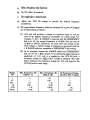
TEST INSTRUMENT SAFETY
WARNING
Normal use of test equipment exposesyou to a certain amount of danger from electrical shock
becausetesting must often be performed where exposedvoltage is present. An electrical shock
causing 10miliamps of current to pass through the heart will stop most human heartbeats. Voltage
as low as 35volts dc or ac rms should be considereddangerousand hazardous sinceit can produce
a lethal current under certain conditions. Higher voltagespose an evengreater threat becausesuch
voltage can more easilyproduce a lethal current. Your normal work habitis should include all accepted practices that will prevent contact with exposed high voltage. and that will steer current
away from your heart is case of accidental contact with a high voltage. You will significantly
reduce the risk factor is you know and observe the following safety precautions:
Don't expose high voltage needlessly. Remove housings and covers only when necessary.
Turn off equipment while making test connections in high-voltage circuits. Discharge highvoltage capacitors after removing power.
Use an insulated floor material or a large, insulated floor mat to stand on, and an insulated
work surface on which to place equipment; and make certain-such surfacesare not damp or
wet. Where insulated floor surface is not available, wear heavy gloves.
3. Use the time-proven "one hand in the pocket" technique while handling an instrument
probe. Be particularly careful to avoid contacting a nearby metal object that could provide a
good ground return path.
Always use an isolation transformer to power transformerless "hot chassis" equipment,
whereone side of the ac power line is connected directly to the chassis.This includes most recent television sets and audio equipment. Without an isolation transformer, the chassisof
such equipment may be floating at line voltage (120 VAC, 60 Hz in USA), depending upon
which way the 2-wire ac power plug is inserted. Not only does this presenta dangerousshock
hazard if the chassisis touched, but damageto test instruments or the equipment under test
may result from connecting the ground lead of some test instrumentsto a "hot" chassis.The
ground lead of this function generator and most other test instruments with 3-wire power
plugs is at earth ground.
S. On test instruments or any equipment with a 3-wire ac power plug, use only a 3-wire outlet.
This is a safety feature to keep the housing or other exposed elementsat earth ground.
6. If possible, familiarize yourself with the equipment being tested and the location of its high
votage points. However, remember that high voltage may appear at unexpected points in
defective equipment.
Also remember that acline voltage is presenton some power input current points suchas on.
off switches, fuses, power transformers, etc., even when the equipment is turned off.
8. Never work alone. Someoneshould be nearby to render aid if necessary.Training on CPR
(cardo-pulmonary resuscitation) first aid is highly recommended.
FOR
.' .6460
W. Cortland
Street
Chicago, Illinois 60635
TABLE OF CONTENTS
PAGE
PANEL
OPERATING
SPECIFICATIONS.
INTRODUCTION
CONTROLS
INSTRUCTIONS
AND
3
FEATURES.
3
5
A.
APPliCATIONS
Frequency
B.C.D.TTLOutput
DC
Voltage-Controlled
and
Waveform
Selection,
Output.
Manual
8
9
10
Operation
Operation.
12
.C.
THEORY
B.
A.D.
Tone
Amplifier
G.
H.
I.
J.
K.AdditionalApplications
F.AMReceiverAlignment Using
E.SpeakerSystemTesting
Digital
Communications
Preset
Control
OF
the
Performance
Overload
Frequency
Frequency
FrequencyOPERATION
Test.
Characteristic. Response.
3010
As
Receiver
Selection.
Selection.
A
Bias
Evaluation
Using
and Alignment.
Signal
Square
Waves
13
13
13
16
18
Source.
18
2021
22
23
23
MAINTENANCE
Detailed
GeneralCircuitDescription
Circuit
Description.
AND
CALIBRATION
25
27
ONE-YEAR
WARRANTY
Removal
Calibration
LineVoltageConversion
liMITED
of
SERVICE
Procedure
Rear
Case
WARRANTY.
INSTRUCTIONS.
31
32
36
3738
'-
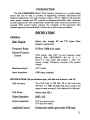
INTRODUCTION
The B & K-PRECISIONModel 3010 Function Generatoris a versatilesignal
source that can be used in a variety of engineering,industrial, educationaland
hobbyist applications.The wide frequencyrange(.1 Hz to 1 MHz) for all functions
(sine, square,triangle and TTL output) encompassessubaudible,
audio,ultrasonic
and RF applications.The continuouslyvariableDC offset control and provisionfor
external VCO control further enhancethe versatility of this instrument. The
human-engineered
caselendsitself to benchuseas well aseasyportability.
SPECIFICA
nONS
GENERAL
BasicOutputs
Square, sine, triangle, DC and TTL Square Wave
(separateoutputjack).
FrequencyRange
OJ Hz to 1 MHz in six ranges.
External Frequency
Control
VCO; greater than 100: 1 on any frequency range
(linear). With FREQUENCY dial set at .1, a
0-to-5.5 V ramp input will produce a 100:1 frequency change. Frequency increases with positive
voltage.
MaximumInput
:!:20V peak.
Input Impedance
1000ohms,nominal.
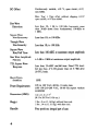
SPECIFICAnONS (AU specifications apply with dial scale between 1 and 10)
Dial Accuracy
5% of full scale to 500 kHz, 8% of full scale from
500 kHz to 1 MHz (includes dial scale accuracy and
range-to-rangeaccuracy). Unit calibrated at full scale.
Dial Range
Greater than 100: 1,
Output Impedance
600.Q, :1:5%.
Output Amplitude
20 V pop open circuit;
10 V popinto 600il.
Amplitude Control
Continuouslyvariable,greaterthan 30 dB range.
3
Max.
DC Offset
Continuously variable, :tIO V, open circuit; :tS V,
into 600Q.
V AC + Voc offset without clipping, :1:10V
open circuit; :1:5V into 600il.
SineWave
Distortion
Less than 1%, 1 Hz to 100 kHz; hannonics more
than 30 dB down from fundamental, 100KHz to
1 MHz.
SquareWave
Non-Symmetry
Lessthan 1%,to 100KHz.
TriangleWave
Non-linearity
Lessthan 1%,to 100KHz.
SquareWave
Rise/FallTime
less than 100nSEC at maximum output amplitude.
SineWaveAmplitude
flatness
:1:.3dB to 1 MHz at maximum output amplitude.
TTL Square Wave
Response
Short-Term
Stability
Less than 25 nSEC rise/fall time. Fixed TTL level:
LO less than .4 V; III greaterthan 2.4 V. Will drive
20 TTL loads.
.05%
PowerRequirements
105 to 130 VAC, 60 Hz. 8 watts max.
(105-130/210-260VAC, 50/60 Hz export version
available)
Dimensions(HWD)
3.2 x 11.3 x 7.7
(8.13x28.70x 19.56 cm.)
Weight
21bs.,9 oz. (1.16 Kg.) without line cord.
21bs., 14 oz.(1.31 Kg.) with line cord.
Handle
Four positions: integralpart of case.
4
"
2.
3.
4.
6.
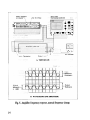
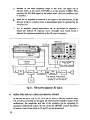
PANEL CONTROLS AND FEATURES
(SeeFig. 1)
1. POWERon-off switch. Depressingthis button turns the 3010on. To turn off,
pushagainand release.
RANGE selectors.Decadefrequencytype. Multiplying the rangeselectedtimes
the FREQUENCYdial (6) indication givesthe output frequency,whichapplies
for all functions. For example,if the 100K RANGE button is depressed
and
the FREQUENCYdial is at 10,the output frequencyis 1 MHz.
FUNCTION selectors.Select square (IUU), sine ("",,),
or triangle ("""")
output waveformwhich appearsat 600n OUTPUTjack (9).
AMPliTUDE control. Controls the amplitude of the output signal, which
appearsat 600n jack (9). This control does not apply to the DC OFFSET
voltageor to the TTL output.
S. DC OFFSET control. Adds positive or negativeDC componentto the signal
appearing at 600n OUTPUT jack (9). Continuously variable for :!:SV
(600 ohms) or :!:10V (open circuit). The DC componentaddedby this control
is dependentof the adjustmentof AMPLITUDE control (4).
FREQUENCYdial. Multiplying the setting of this dial times the frequencyof
the RANGE switch (2) selectedgivesthe output frequencyof the waveformsat
the 600n OUTPUTjack (9) and TTL jack (7).
7. TI'L jack. A TI'L square wave is available at this jack. The frequency is
determinedby the RANGE selectedand the settingof the FREQUENCYdial.
This output is independentof the AMPliTUDE and DC OFFSETcontrols.
8. -=b(Ground)jack. Commonreferencefor the 1TL and 600n OUTPUTsignals.
9. 600Q OUTPUTjack. Waveformsselectedby FUNCTIONswitchesaswell as
the superimposed
DC OFFSETvoltageareavailableat this jack.
10. HANDLE. Multiple-position design permits use as a tilt stand or carrying
handle.
6
CX)
r
CD,
L!'),
~'
(V)
N
.
+
~"
,~,,';~
"""I'i
--~
0')
-
jj:~:B
¥~:.'
""'."'."""";
~
:D::::~::::
1119,11
'
-
0,
~;
rn
u
E
=
~
~
fn
=
=
"0
(.)
0
=
~
[
=0
ch
~
-
~
11. VCO INPUT jack (rear panel). An externalvoltageinput will vary the output
frequency. The changein frequencyis directly proportional to input voltage;
therefore,the rate of changeof frequencyis proportional to that of the input
voltage.
12. LINE CORD RECEPTACLE (rear panel). This receptacle accepts the
detachableline cord. (Fixed power cord on 105-130/210-260VAC, 50/60
Hz export version.)
11
12
Fig.2. Rearpanel.
7
A.
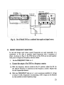
OPERATINGINSTRucnONS
FREQUENCYAND WAVEFORMSELECTION,MANUAL OPERAnON
With the unit pluggedinto a powersource,depressthe POWERbutton (1).
2.
Selectthe frequencyrangedesiredby depressingthe appropriateRANGE
switch. The frequency range obtained as the FREQUENCYdial (6) is
varied will be from one-tenththe indicatedRANGEvalueto 10timesthis
value. For example,selectthe 10 K range.Whenthe FREQUENCYdial is
at .1, the output frequencyis 1 KHz; whenat 1, it is 10KHz and whenat
10 the frequencyis 100KHz. The frequencyobtainedappliesto the signal
at the lTL jack as well asthe 60012OUTPUTjack.
3.
Select the waveform desired by depressing the appropriate FUNCTION
button. The phase relationships of the waveforms available are shown in
Fig. 3.
4.
The amplitude of the selected output signal at the 6001"2OUTPUT jack is
adjusted by AMPLITUDE control (4). The TTL output is not affected by
the AMPLITUDE control.
5,
A DC component can be added to the signal at the 600n OUTPUT jack by
use of the DC OFFSET control. The DC component introduced is
independent of the AMPLITUDE control and does not apply to the TTL
output. The level of DC can be varied :tIO volts open circuited or :tS volts
across 600 ohms.
Fig. 3. Output waveform and phase relationships.
8
7.
A. ZERO DC OFFSET
WITH MAXIMUM
SIGNAL.
B. OFFSET LIMITS
WITHOUT CLIPPING
C. EXCESSIVEOFFSET,
-5V
.-POSITIVE
DC OFFSET
NEGATIVE
DC OFFSET
Fig. 4. Useof DC OFFSETcontrol.
6.
Remember that the output signal swing of the generator is limited to :1:10
volts (open circuit) or :1:5volts into 600 ohms. This applies to the
combined signal and DC offset. Clipping occurs slightly above these levels.
Fig. 4 illustrates the various operating conditions encountered, when using
the DC offset. If the desired output signal is large or if a large DC offset is
used, an oscilloscopeshould be used to make sure that the desired
combination is obtained without undesirable clipping.
Whenusingthe higher output frequenciesand whenusingthe squarewave
and TTL outputs, terminate the cable in 600 ohmsto minimize ringing.
Keepthe cablesas shortaspossible.
B.
DC OUTPUT
The DC OFFSETfeature canbe usedto convertthe Model 3010 to a bipolar
DC power supplywith an internalimpedanceof about 600 ohms.
Depress the FUNCTION switches slightly so that all switches are released
(all buttons out). This removes all signal components from the output.
2. The output now consists of a DC voltage which can be varied continuously
from -10 volts to +1 0 volts (open circuit) by use of the DC OFFSET
control.
9
2.
A decoupling capacitor (20 mfd or more) can be connected across the
60012 OUTPUT and ground (-=:!::-)
terminals to reduce the AC impedance
of the output. Always observe polarity when using polarized capacitors.
c.
VOLTAGE-CONTROLLEDOPERAnON
The 3010 can be operatedas a voltage-controlledoscillator(VCO) by usingan
external control voltageapplied to the VCO IN jack at the rearof the unit. A
male phono plug is provided for this purpose.The externallyappliedvoltage
will vary the frequencywhich is preselectedby the RANGE switchesand the
FREQUENCYdial. A positive-goingvoltage will increasethe frequencyand a
negative-goingvoltage will decreasethe frequency. Pleasenote that the
frequency does not change without limit as the input control voltage is
increased.The upper dial frequencycan be exceededby about 10 percent. If
the control voltagereducesthe lowest frequencyavailablebelowthe frequency
correspondingto the low end of the frequencydial (.1), erratic operation
results.
The desired frequency, output waveforms, DC offset, and the output
amplitud& adjustment are selected as for manual operation. The maximum
voltage-controlledsweepis overa 100:1 range.
SWEEPFREQUENCYOPERAnON
a.
Selectfrequencyrangeand function.
b. SetDC offset, if required.
c. Setamplitudeto desiredlevel.
d. To obtain maximum sweep, set the FREQUENCYdial to either
extreme. For this example,set at low end(.1 on FREQUENCYdial).
e. Connecta positive-goingvoltageto the VCO IN jack. A 0 to +5.5 volt
ramp will provide a frequency increasecorrespondingto a FREQUENCY dial setting of 10. This is a 100:1 ratio. The frequency
variesin direct proportion to the appliedinput voltage.
FREQUENCYMODULATION
If an alternatingvoltage with no DC componentis appliedto the VCO IN
jack, the preset frequency will vary aboveand b~low the frequencythat
was preset by the RANGE switch and FREQUENCY dial. The DC
component of such an input signal can be removedby transformeror
capacitivecoupling.
10
Min. M
Max.
K
KKK
KK
a.
Selectfrequencyand function.
b. SetDC offset, if required.
c. Setamplitudeto desiredlevel.
d. Adjust the VCO IN voltage to provide the desired frequency
modulation.
e. The approximatefrequencydeviationobtainedfor a givenVCOsignal
canbe determinedasfollows:
(1) .055 volt will produce a changein frequencyequal to one per
cent of the highest frequencyobtainable on a givenrange.For
example,if the 1 K RANGE is selectedand the FREQUENCY
dial is at 10, the output frequencyis 10KHz. One per cent of
10 KHz is 100Hz. Therefore,for each .055 volt changein the
VCO voltage,a 100Hz changein frequencyis producedwith the
1 K RANGE selected,regardlessof FREQUENCYdial setting.
(2) As an example,assumethe RANGE switch and FREQUENCY
dial are set for 5 KHz output. If an alternatingsignalhavingan
amplitude of :t.55 volt is is applied to the VCO IN jack, a
frequencyswing of :t (:ih) 100 = :tl KHz is obtained.The table
below indicatesthe frequencychangeper .055 volt input to the
VCO IN jack for eachrange.
Range,
Hz
1
10
100
1:
10 K
100 K
Frequency,Hz
(Dial at .1)
.1
1
10
100
1
10
Frequency, Hz
(Dial at 10)
1%FrequencyChange,
Hz (For .055 V input)
10
100
1
10
100
1
10
100
lK
lOK
3.
D. lTL OUTPUT
This is a fast rise time square wave output, available at the front panel. Because
of the fast transition times of this output, cabie termination should be
provided to minimize ringing. The output is always positive with respect to
ground. This signal can be'used as an external sync pulse for oscilloscopes when
using the other generator outputs. It also can be used as a variable frequency
signal source for exercising logic circuits.
1. Selectdesiredfrequency(repetition rate).
2. Connectto TTL output.
The AMPliTUDE and DC OFFSETcontrolshaveno effect on the TTL
output signal.
12
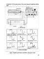
AMPUFffiR FREQUENCYRESPONSE
(SeeFig. 5)
1. Interconnect equipment as indicated Fig. SA. This use of either the oscilloscope or the AC voltmeter to measure output voltage is adequate. The
advantage of the oscilloscope is that waveform distortion can be
simultaneously monitored, particularly if a power responsecurve is being
run. The AC voltmeter, provided with decibel scales,is convenient for
converting the observed output variations into standard units of measurement (dB). The amplifier under test may be anything from a single stage
transistor amplifier to a higi1 fidelity component type. The dual trace
oscilloscope is convenient for this application because the -input to the
amplifier as well as the output c~ be monitored simultaneously.
Vary the frequency of the 3010 as required, maintaining a constant
amplitude as observedon the oscilloscope.The amplifier input and output
waveformscan be monitored simultaneouslyasindicatedin Fig. Sb.Using
two centimetersfor amplitudereferencesprovidesa convenientmethod of
determiningpercentof changein amplitude.
The resultsof responsetestscan be plotted on semi-logpaperasindicated
in Fig. 6.
TONE CONTROLTEST
If the amplifier under test is provided with baseand treble controls, the effects
of these controls on overall responsecan be determined by running consecutive
response curves with the controls at both extremes of adjustment. The results
can be plotted on semi-log graph paper, as indicated in Fig. 7.
C. AMPliFIER OVERLOADCHARACTERISTIC
1.
A.
APPLICATIONS
3.
B.
2.
The overload point for some. amplifiers is difficult to determine exactly
because of the gradual overload characteristic. The exact point of which
signal compression begins is difficult to determine using sine-wave input.
The triangle wave form is ideal for this type of test becauseany departure
from absolute linearity is readily detectable.
Using the test set-upof Fig. SA and using the triangle output, the peak
overload condition for an amplifier can be readily determined. This
overloadcondition is shownin Fig. 8.
13
..
D-1
.0
Select waveform
as required
\
Dual Trace
Oscilloscope
No DC Offset
preferred
; .C8)-1
I
~II DDDDD"DDDDD
0"0
.[[]. [[].111...~
I-u=J
Amplifier
-u
;r;::'1
under test
-0
--+--i
..
Termination
AC Voltmeter
Output
A. TESTSET-UP.
B. WAVE SHAPEAND AMPUTUDE.
Fig. 5. Amplifier frequencyresponse,
manualfrequencychange.
14
..20"
In +...
-a
W
(/)
+5
~
(/)
w
~
0
w
>
'
~
I
~ -10
-20.1
FREQUENCY. Hz
Fig. 6. Plot of amplifier frequency response.
+201
~ ..101
.
L1J
II)
1
Z
+51
ffi
0
0
Do
a:
L1J
>
I
-5
-'ij
L1J -10
a:
FREQUENCY,
Hz
Fig. 7. Tone control effectiveness.
15
2.
4.
Input
Waveform
Output
Waveform
Fig. 8. Amplifier overloadcharacteristics.
D. AMPliFIER PERFORMANCEEVALUAnON USING SQUAREWAYES
The standard sine-wavefrequencyresponsecurves,suchas thoseobtained in
Par. A, do not give a full evaluationof the amplifier transientresponse.The
square wave,becauseof the high harmonic content, yields much information
regarding amplifier performance,when used in conjunction with an oscilloscope.
Usethe test set.upof Fig. 9A. This is similarto that usedin Fig. SA except
that a terminationis specifiedat the; !mplifier input. This is essentialwhen
using squarewavesto eliminate the ringing effects generatedby the fast
risetimes.
Using the triangle output of the 3010, set the AMPliTUDE control so
that there is no signalclipping overthe rangeof frequenciesto be used.
Selectthe squarewave output and adjustthe frequencyto severalcheck
points within the passbandof the amplifier, such as 20 Hz, 1000Hz and
10KHz.
At each frequency check point the wave form obtained at the amplifier
output providesinformation regardingamplifierperformancewith respect
to the frequencyof the squarewaveinput. Fig. 9B indicatesthe possible
waveforms obtainedat the amplifier output and the causes.
Square wave evaluation is not practical for narrow band amplifiers. The
restricted band width of the amplifier cannot reproduce all frequency
16
componentsof the squarewave in the proper phaseand amplitude relation-
ships.
Dual Trace
Oscilloscope
rNo DC Offset
preferred
"'°1111
8
88-
'-Square wave
selected
.~
\;:~m.rn.-~ ~ .~
I
Amplifier
under test
-<>
0-1
-t
-0
Termination
Output
I
A. TEST SET-UP.
B. TESTWAVEFORMS.
Fig. 9. Amplifier performanceevaluation,usingsquarewaves.
1'7
2.
4.
E.
SPEAKERSYSTEMTESnNG
The 3010 canbe usedto provideinformation regardingthe input impedanceof
speakersystemsvs. frequency.In addition,the low-frequencyresonanceof the
system can be determined. Becausethe Model 3010 output impedanceis
600 ohms, which is much higher than the impedanceof conventionalspeaker
systems,the 3010 can be used as a variable.frequency current source to
evaluatethe input impedanceof.the speakersystem.This is shownin Fig. lOB.
1
Use the test set-upFig. lOA. An oscilloscopecould be usedin this set-up
to verify that the 3010is not beingoperatedin a clipping condition.
Vary the frequencyof the 3010 over the full rangeof interestandlog the
voltagemeasuredat the speakerterminalsvs. frequency.The dB scalesof
the AC voltmeter are convenient for converting this information to
standardresponseunits.
3. It will be observedthat at somelow frequency,a pronouncedincreasein
voltage will occur. This is th~ resonancefrequencyof the low-frequency
driver in the speakersystem.This test set-upis convenientwhendesigning
speakerenclosures.It can help the designerto determinethe effect on
systemresonanceof varying port sizes,dampingmaterialsand otherbasic
enclosurefactors.
The measurements
obtained in the abovetestscan be plotted on semi-log
graphpaperasindicatedin Fig. IOC.
F-
AM RECEIVER AUGNMENT
1
Use the test set-upof Fig. 11. Becauseof the linear relationshipbetween
sweep voltage and frequency of the Model 3010, a linear frequency
presentationis obtained on the oscilloscope,regardlessof whether the
sweepvoltageis a triangle,sinewaveor a ramp.
2. To minimizethe numberof set-upadjustmentsrequired,the sweepvoltage
to the VCO IN jack of the 3010 should not havea DC component.This
canbe removedby capacitorcoupling.
3. If a precise center frequencyis required,a frequencycountershould be
used when setting the output frequencyof the 3010. This is done without
sweepvoltageinput.
The sweepvoltageto the oscilloscopecanbe suppliedeitherto anexternal
horizontal input jack or, if the oscilloscopehas front panelX-Y capability,
it canbe appliedto one of the two vertical input jacks.
Fig. 10. Speakersystemtests.
IQ
5.
Becauseof the wide frequency range of the 3010, the signal can be
injected either at the mixer (455 KHz) or at the antenna(1 MHz). When
injecting the 455 KHz signal at the mixer input, the local oscillator must
be disabled.
6.
When the IF response is observed at the input to the AM detector, an RF
detector probe is required unless a demodulated point is specified by the
manufacturer.
7.
The IF amplifier tuning adjustments can be performed as required to
obtain the desired IF response curve. Normally each tuned circuit is
adjusted for maximum amplitude at the IF center frequency.
Fig. 11. AM receiveralignment,RF and IF.
G.
USING mE 3010 AS A BIAS AND SIGNAL SOURCE
In the test set-upof Fig. 12 the 3010 can be usedto biasthe transistorunder
test as well asto furnish an AC signal.By observingthe amplifier output on the
oscilloscope,the amplitude and bias of the transistorcan be optimized for
maximumundistorted output. By useof the DC OFFSETcontrol, the effects
of varioustypes of bias(classA, B, and C) canbe determined.
20
2.
3.
21
Dual Trace
DC
Offset
~\
Oscilloscope
as required
Scope Sync
if required
preferred
~1.=...:;m~]]-~-~
A+
:
waveseIec~ I
u
o4oj
Fig. 12. Useof Model 3010 asa combinedbias'supplyand signalsource.
H. PRESETFREQUENCYSELEcrION
In test and design work where severalfrequenciesare used repeatedly,it is
convenient to be able to preselectthese frequencieswith a minimum of
effort. As shownin Fig. 13, the VCO featureof the 3010canbe usedtogether
with presetvoltagesand frequencyselectorswitch.
1. Setthe FREQUENCYDIAL to .1.
Connectthe output of the 3010to a frequencycounter.
With the frequency selectorswitch in the Fl position, adjustthe Rl for
the desiredfrequencyas observedon the frequencycounter. Repeatthis
for the frequenciesdesired.
4. With the FREQUENCYdial set at .1, anda maximumavailableA+ voltage
of about 6 volts, frequenciesencompassing
a 100:1 rangecanbe obtained
by this method on eachfrequencyrange.
Fig. 13. Presetfrequencyselection.
I. DIGITAL FREQUENCYSELECTION
Frequenciescan be switched electronically by using the set-up shown in
Fig. 14. The presetvoltagescanbe digitally selectedand appliedto the VCO IN
jack on the Model3010. Although provisionsfor two frequenciesare shown,
additional frequencies can be added using redundant circuits. This is
convenientin frequencyshift keying (FSK) systems.
+6V
Fig. 14. Digitally programmedfrequencyselection
22
J. COMMUNICAnONSRECEIVERAUGNMENT
The test set-upof Fig. 15 canbe usedfor alignmentof communicationreceiver
IF's arid discriminators using the 455 KHz IF frequency. For accurate
frequency adjustments,a 455 KHz crystal control marker sourceshould be
used.
The sweepvoltagesourceis applied to the 3010 VCO IN jack and to the
oscilloscopeX-axisinput.
2.
the IF response curve is indicated. In some receivers the IF selectivity is
"packaged" which means all adjustments are preset. In this case the
receiver alignment can only be evaluated and verified without adjustment.
Where the tuned circuits are adjustable, the manufacturer's procedure
must be followed to insure that the proper overall responseis obtained.
K. ADDInONAL APPliCATIONS
The triangle output of the 3010 can be used at its lowest frequencies to
simulate a slowly varying DC source. This can be used to check threshold levels
of TfL and CMOS logic as well as voltage comparators. Chart recorders can be
checked by this method. Analog meter movements can be exercised from zero
to fu" scale to observe defects, such as sticky meter movements.
23
Jj
~ ~
-\j
FM Receiver
A.
A
\j
435
E
455
Fig. 1S. Alignmentof communicationsIF's and discriminators.
24
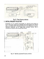
THEORY OF OPERATION
GENERAL CIRCUIT DESCRIPTION (See Block Diagram and Schematic)
The basic waveformgeneratedin the Model 3010 is the trianglewave.This is
accomplishedby charging and then discharginga capacitorby equal magnitude
currents. A dual comparatorand flip flop determinewhetherthe capacitoris being
chargedor discharged.Whenthe voltageon the capacitorreachesthe positivelimit,
the charging current is switched off and the capacitordischargesuntil the lower
limit is reachedat which time the chargingcurrentis thenreapplied.The output of
the dual comparatoris a squarewave.
To produce a sine wave,the triangle wave is shapedby a specialamplifier.
Rangeswitchingis accomplishedby changingthe magnitudeof the currentsources
and the timing capacitor.Dial frequencytuning is doneby changingthe magnitude
of the current sources.A frequencychangeof over a 100:1 is possiblewith the
frequencydial. Belowis a table of the capacitorsand currents.used.
RANGE (100:1)
Hz
1Hz
10Hz
100 Hz
CAPACITOR
-10Hz
3.31J.F(CI5)
-100Hz
3.3 pF (CIS)
-1
-10
KHz -100
10 KHz -1
KHz
KHz
KHz
MHz
033 .uF (C16)
033 JJ.F(C16)
325 pF(CI7, 18)
300 pF (C18)
CURRENT
1.65 IlA -165 IlA
16.5,uA
-1.65
65 JlA -165
16.5.uA
mA
JlA
-1.65
mA
.65 .uA -165
.uA
16.5 IlA
-
65mA
The peak-to-peakvoltage of the triangle wave generatedis 2.5 V. The
frequencyof operationis determinedby the currents,the capacitorvalueand the
peak-to-peakvoltageof the trianglewave.
25
26
Tuning
B.
D.
.
f = (2)-ccr
"-(Vpp)
Thus for I = 1.65 mA, C = 3.3 jJ.Fand Vpp = 2.5 V
1.65xx110-3
f = (2) (3.3
0~6) (2.5)
f= 100 Hz
DETAILED CIRCUIT DESCRIPTION
A. FrequencyControl VoltageReference(IC4B)
The Frequency Control Voltage Reference is composed of three trimpots
(Rll, 12, 13), two resistors and IC4B, which divide the +15 volts supply and
provide a reference voltage of approximately + 12 volts to the Frequency
Control Potentiometer. Each trimpot is adjusted to compensate for the
tolerance variations of the timing capacitors.
Amplifier (IC4A)
The tuning amplifier is provided to buffer the output of the Frequency Control
Pot. This assures that this voltage will be as linear as the frequency pot RIOI
itself. If not, Rl7 would be in parallel with frequency pot RIO1 and the action
of the frequency pot would be non-linear.
c.
CurrentSummingAmplifier (IC4D, Q3)
The current Summing Amplifier sums the current from the tuning amp and the
VCO input. The current from the tuning amp is simply the voltage at its output
divided by the value of R17 (2Kil), The current from the VCO input is
normail.y zero. When a voltage is applied, the current into the summer is the
voltage divided by R18 (lKil).
For a 100:1 sweep, the voltage has to be
approximately +5.5V. The output current (collector of Q3) creates a voltage
across R19 (1 K) that tracks the voltage of the tuning amplifier by a factor of
-%.
Current Source Driver (IC3D, Q4)
IC3D is an operational amplifier and. Q4 is an emitter follower used in
27
E.
F.
28
conjunction with the operational amplifier. IC3D and Q4 are connected as a
voltage follower with a closed loop gain of + 1. The voltage of the emitter of Q4
follows the input voltage of pin 12. The voltage at the collector of Q4 tracks
the voltage at the emitter but is of opposite polarity. In tflis way the current
source driver provides both current sources with equal voltages.
Positive& NegativeCurrentSources(IC3A, IC4C,Q5, Q6)
TIle current sources provide two switchable sets of currents,. IC3A and Q6 are
connected as a voltage follower. The voltage at the emitter of Q6 is equal to
the voltage at the input to IC3A (pin 3). The current, produced, -I, is equal to
the -15 volt supply minus the voltage at the emitter of Q6, divided by the total
resistance RTI (which equais R22 + R23). The current -101 is produced by the
same voltage but R24 has been switched in paraUeito the sum of R22 + R23
and the total resistance is now the parallel combination RT 10 (R24 in parallel
with the sum of R22 + R23).
The voltage across R21 is equal and opposite to the voltage acrossR20. IC4C
and Q5 are connected as a voltage follower similar to IC3A and Q6. The
voltage at the emitter of Q5 is equal to the voltage at the input to IC4C (pin
10). The current produced is equal to the + 15 volt supply minus the voltage at
the emitter of Q5 divided by the total resistance RT2 (which equals R25 +
R26). The value of RT2 is half the value of RT l' therefore the current is 21.
Similarly, when the combination, R27 + R28, is switched in parallel to the
combination R25 + R26, the total resistance is RT20, which equals R25 +
R26, in parallel with R27 + R28. The total current with RT20 is 201.
Diode Gates (05, 06)
The diode gates are silicon diodes D5 andD6. In the 1.100 and 10K range,the
positive current source puts out 21 and the negative current source sinks -I
current. The purpose of the gates is to either switch the output of the positive
current source to the capacitors to charge them, or to shunt the current so that
the negative current source can discharge the capacitors. The gates work as
follows:
If the signal from the level detector is high-level TTL, +5 V, it
reverse-biases diode D6 and cuts it off. Diode D5 now becomes
forward-biased and all the current (21) flows through D5. Since the
negative current source can only sink -I current, a net positive current, I,
is seen by the capacitors and they are linearly charged to produce a
positive ramp.
If the signalfrom the level detectoris low-levelTTt, 0 V, it forward-biases
diode D6 and the level detectorsinks all the current (21),from the positive
current source. Diode DS now becomesreverse-biased
and no current
flows thru it. The capacitors now see only the negative current source with
-1 current and are linearly discharged to produce a negative ramp. In the
10, lK, and lOOK ranges the gates work exactly the same except that the
currents are now 10 times greater.
G. CT (CIS, 16,17,18)
The timing capacitorsCT are chosenfor suchhighly desirablequalitiesas:
Low dissipationfactor.
Low temperature coefficient.
3. Long-termcapacitancestability.
H. TriangleBuffer (Q7, Q8)
The triangle buffer hasa veryhigh impedanceto minimizeleakagecurrentsand
preventloading of the timing capacitors.Q7is a dual FET; onehalf is the high
impedancebuffer to the capacitorswhile the other half providestemperature
compensationto the first half. Q8 is an emitter follower and is usedto provide
the necessarycurrent to drive the level detector,sine shaper,etc. The three
silicon diodes along with the base-emitterjunction of Q8 shifts the triangle
waveform seenat the emitter of Q8 up to four diode drops (about 2.6V) so
that the diode datescan switch properly with a TTL levelsignalfrom the level
detector.
Dual LevelDetector& Flip-Flop (ICS)
The level detector senses the level of the ramp input (either positive or
negative) and switches output states when the input reachesanyone of two
voltage limit references. The device (75107) has a dual differential input
comparator stage and a dual three-input nand gate output stage connected as
an R-S flip-flop. The input limit voltage references are set by two voltage
dividers on the tracking + 15 V and -15 V supplies. Resistors R32 and R33 set
+ 1.25 V for the minus input of one comparator. Resistors R34 and R35 set
-1.25 V for the plus input of the other comparator. C22 couples a small positive feedback from one output of the iine receiver (pins 5 & 9) to the inputs
(pins 2 & 12) to speed up the switching.
J. TTL Buffer (IC6B, IC6C)
IC6B and 6C are half of a quad nand gate package. They are connected in
p'.frallel and provide a fan-out of 20 for the TTL square wave. This avoids any
loading on the level detector.
29
M.
N.
K. Square Wave Level Shifter (IC6A, IC6D)
The squarewave level shifter shifts the DC levelof the lTL output of the level
detectorso that it is approximatelysymmetricalaboutzero.IC 6A and6D are
connectedin parallel.One setof inputs (pins 2 and 12)areswitchedso that the
level shifter operates only when the square function button is pushedon.
Trimpot R42 providesanamplitude adjustmentfor the squarewave.
L. SineWaveShaper (IC7)
The sine wave shaper takes a triangle wave input and non-linearly shapesit to
produce a sine wave. Tfie shaper utilizes the non-linear relationship of a
differential pair of transistors. The output is taken from one collector of the
pair and buffered and level-shifted by the two other transistors in the package
IC7. Trimpot R52 adjusts the amplitude of the sine wave and R59 adjusts its
DC level at the output. Trimpots R50 and R55 are adjusted to provide the
lowest distortion of the sine wave.
Output Amplifier (Q9, 10, 11, 12, 13)
The Output Amplifier consistsof .a differential input stage(Q9 and Q10)
followed by a common emitter transistor, Q11. The output from Q11 is
applied to a push-pulloutput stage(Q12 and Q13). Feedbackis appliedfrom
the output to the base of Q10 by R70 and R69. The closed loop gain is
approximately10. DC offset is obtained by applying the offset voltageto the
baseof Q10 also.
PowerSupply (IC1, IC2, IC3B, IC3C, Ql, Q2, 01,2,3,4)
Power transformer Tl, bridges diodes Dl, 2, 3, 4 and fIlter capacitors Cl and
C3 generate +22 V and -22 V unregulated. The +22 V is applied to ICl, a
78L15A voltage regulator, which generatesthe + 15 V supply. The +22 V is also
applied through R5 to IC2, a 78LO5A regulator, which generates the +5 V.
IC3C and Ql comprise a -15 V regulator which is referenced to the +15 V via
Rl and R2. In a similar manner, IC3B and Q2 comprise a -5 V regulator which
is referenced to the +5 V supply via R7 and R8.
30
MAINTENANCE AND CALIBRATION
The following instructionsare for use by qualified personnelonly. To
avoid electric shock,de not performservicingotherthan containedin
the operatingirtstructionsunlessyou arequaIifiedto do so.
2. A shockhazardis presentwhenthe caseis removedoncethe line cord
is pluggedinto an AC outlet. Avoid touching the fuse or bottom of
ilie circuit board in the area of the fuse or powertransformer.The
fusehas 120 VAC (240 VAC on export models)on it evenwhenthe
POWERswitchis off.
Your B & K-PRECISION Model 3010 Function Generator was carefully
checked and calibrated at the factory prior to shipment. Calibration of this
instrument should not be attempted unless you are experienced and qualified in the
use of precision laboratory equipment. Should any difficulty occur during repair or
calibration, refer to the warranty service instructions at the rear of this manual for
information or technical assistance.
Screw
Fig. 17. Removalof rearcase.
31
4.
B.
2.
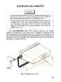
REMOVALOF REAR CASE
To remove the rear case from the generator, proceed as follows:
Usea coin (a quarter works best)to removethe two screwsthat hold the
handle to the case.Use caution to avoid losing the springsbeneaththe
screwsthat hold the handle on the case.Removethe handle.The handle
maybe reversedif the userdesires;referto Fig. 17.
2.
Remove the two Phillips head screwsfrom the rear case.
3.
Slidethe rearcasefrom.the generator.
To re-install the rear case on the generator, follow the above procedure in
reverse. When re-installing the rear case,be sure the printed circuit board
properly engagesthe slots inside the case.
CALIBRAnON PROCEDURE
A. EquipmentRequired:
Tektronix Model465 Oscilloscope.
2. Hewlett-PackardModel 333A Distortion Analyzer.
3. B & K-PRECISION Model 1820 Universal Frequency Counter.
600[2 Tenninating Resistor.
Procedure:
Remove3010 rearcaseReferto Fig. 17.
Place the 3010 on an insulated surface. Plug the line cord into the
receptacle on the 3010 rear bracket, then plug the other end into a
120 VAC outlet.
3.
Set
up
POWER.
RANGE
the
3010
controls
as
follows:
.
ON
100
DC
AMPLITUDE
FREQUENCY
FUNCTION
OFFSET
TRIANGLE
Centered
Fully Counterclockwise
10
Referto Fig. 18 for trimpot location and Table for trimpot function.
32
~R52
~F1
~R55
iR50
~R59
Fig. 18. Trimpot location.
Trimpot No.
Function
R26
R28
R42
R50
R55
1 KHz Symmetry
10 KHz Symmetry
Square Wave Amplitude
Sine Distortion 1
Sine Distortion 2
R52
Sine WaveAmplitude
Sine WaveDC Level
10 K Range Frequency
1 K & 100 Range Frequency
10 & 1 Range Frequency
R59
R13
R12
Rll
TableI. Trimpot Function
33
4. Symmetry Adjustments (Refer to Fig. 18 for location of Trimpots R26
and R28).
Terminate the 30 I 0 TTL OUTPUT with 6O0n an~ connect both channel
I and channel 2 scope probes to it. Set the scope controls asfollows:
CH 1 VOLTS/DIV
CH 1 COUPLING
CH 2 VOLTS/DIY
CH 2 COUPLING
CH 2 INVERT. .
VERT MODE ...
A TIME BASE..
IV
DC
IV
DC
INVERT
ALT
.1 mS/DIV
{LOCK
HORIZ DISPLAY
A TRIG
MODE.
A COUPliNG.
A TRIGGER
SOURCE
B COUPLING.
A
..
...
SCOPE
...
BSOURCE
KNOBS
AUTO
DC
NORM (Important)
+
DC
STARTSAFTER DELAY
Adjust CH 1 and CH'2 positioncontrolsto centereachtraceand adjustA
TRIGGER level for a stabletrigger. The displayshould appearto be two
squaresin phasebut sinceCH 2 is invertedand NORMsourcetriggeringis
used,what appearsto be falling edgeof CH 2 is actually the leadingedge
of the TTL OUTPUT.
Change HORIZ DISPLAY to A INTEN.
Use the B TIME/DIY KNOB (pull to unlock) and the DELAY TIME
POSITION CONTROL to center the intensified trace to the trailing edges
of the square waves. Continue until the B TIME/DIY setting is IllS/DIY.
Now change HORIZ DISPLAY TO B DLY'D and the display should show
an expanded view of the falling edgesof the square waves.
Adjust Trimpot R26so that the edgescoincide.
Change the 3010 RANGE setting to 1 K and repeat the above procedure
but change A TIME/DIY to 10 pS/DIY and B TIME/DIY to .1 pS/DIY
and adjust Trimpot R28 sO that the trailing edgesof the two square waves
coincide.
34
7.
Amplitude Correlation and Sine Distortion Adjustments.Terminatethe
3010 600Q OUTPUTwith 600Q and connectchannell scopeprobeto it.
Changethe scopecontrolsto the newsettingsasfollows:
CH
1 VOLTS/DIY
.
CH
1 COUPLING.
.
TIME
VERT
BASE.
MODE.
2V
GND
CHI
1 mS/DIV
HORIZ DISPLAY.
LOCK
A KNOBS
Adjust CH 1 POSITIONcontrol to centerthe trace on the scopegrid. Flip
CH 1 COUPLINGto AC. Pushin the 3010100 RANGE button and rotate
the 3010AMPLITUDE knob clockwiseuntil the trianglewavejust touches
the 0 and 100 dotted lines on the scopegrid. Flip CH 1 COUPLINGto
DC. Rotate the 3010 DC OFFSET knob until the triangle wave just
touchesthe 0 to 100dotted lines on the scopegrid.
Pushin the 3010 SQUAREFUNCTIONbutton. Flip CH 1 COUPLINGto
AC. Adjust Trimpot R42 until the squarewavejust touchesthe 0 and 100
dottedlines on the scopegrid.
6.
Push in the 3010 SINE FUNCTION button. Connect the distortion
analyzerto the 3010 600Q OUTPUT. Manipulatethe distortion analyzer
for a minimum distortionreading.Adjust Trimpot R50 first, then Trimpot
R55, for a minimum distortion reading.Readjustboth Trimpots R50and
R55 for a minimum distortion reading (must be less than or equal to
0.5%).Disconnectthe distortionanalyzer.
Adjust Trimpot R52 until the sinewavejust touchesthe 0 and 100dotted
lines on the scopegrid. Flip CH 1COUPliNG to DC. Adjust Trimpot R59
until the sine wavejust touchesthe 0 and 100 dotted lines on the scope
grid.
FrequencyAdjustments.
Connect the counter to the 3010 600il OUTPUT. Set the counter to
PERIOD FUNCTION. Pushin the 301010 K RANGE button and be sure
that the 3010 FREQUENCYdial is set to 10. Adjust Trirnpot R13 for a
counterreadingof 10.000p.S.OK if counterreadingis between9.980p.S
and 10.020p.S:
Push in the 3010 100 RANGE button. Adjust Trimpot R12 for a counter
reading of 1000.00 JlS. OK if counter reading is between 998.000 JlSand
1002.00 JlS.
35
8.
,~
4.
Push in the 3010 10 RANGE button. Adjust Trimpot R11 for a counter
readingof 10.0000mS.OK if counter readingis between9980.00.uSand
10.0200mS.
Disconnectthe scopeprobe and counter from the 3010 600n OUTPUT.
Carefullyre-installthe rearcase(referto Fig. 17)
LINE VOLTAGE CONVERSION
The 105-130volt, 60 Hz power transformer (065-137-9-001)
used in the standard 3010 is replaced by a 105-130/210-260volt, 50/60 Hz power transformer
(065-137-9-002)in the export version. The line cord in the export version uses
standard DIN color codes. The power transformer is normally prewired to
match the power source used in the country of original sale. The instrument
may be easily coverted to the alternate line voltage. To convert from 210-260
volt operation to 105-130volt operation, or vice versa,usethe following pro-
cedure:
Remove case(Fig. 17).
2. Rewire power tansformer for desired line voltage (Fig. 19).
3,
Change fuse Fl (seeFig. 18 for location). Use 'I. A, 3AG slow blow for
105-130volt operation, or ~6 A, 3AG slow blow for 210-260volt opera-
tion.
Change line voltage label.
210-260 V AC
105-130 VAG
Fig. 19. Transformer wiring, export version.
36
WARRANTY SERVICE INSTRUCTIONS
.Refer to the MAINTENANCE section of your B & K-Precision instruction
manual for adjustments that may be applicable.
2. If the above-mentioned procedures do not correct the problem you are
experiencing with your unit, pack it securely (preferably in the original cart()n or
double-packed). Enclose a letter describing the problem-and include your name
and address. Deliver to, or ship PREPAID (UPS preferred) to the nearest
B & K-Precision authorized service agency(see list enclosed with unit).
If your list of authorized B & K-Precision service agencies has been misplaced,
contact your local diskibutor for the name of your nearestservice agency, or write
to:
Service Department
B & K-Precision Product Group
DYNASCANCORPORATION
2815 West Irving Park Road
Chicago, Illinois 60618
37
LIMITED ONE-YEAR WARRANTY
DYNASCAN CORPORATION wanants to the original purchaser that its B & KPRECISION product, and the component parts thereof, will be free from defects in
workmanship and materials for a period of one year from the date of purchase.
DYNASCAN will, without charge, repair or replace, at its option, defective product or
component parts upon delivery to an authorized B & K-PRECISION service contractor or the
factory service department, accompanied by proof of the date of purchasein the form of a sales
receipt.
To obtain warranty coverage, this product must be registered by completing and mailing the
enclosed warranty registration card to DYNASCAN, B & K-PRECISION, 6460 West Cortland
Street, Chicago, Illinois 60635 within fifteen (15) days from the date of purchase.
Exclusions: This wananty does not apply in the event of misuseor abuse of the product or
as a result of unauthorized alterations or repairs. It is void if the serial number is altered,
defaced or removed.
DYNASCAN shall not be liable for any consequential damages,including without limitation
damages resulting from loss of use. Some states do not allow limitation of incidental or
consequential damages,so the above limitation or exclusion may not apply to you.
This warrantygivesyou specificrights and you mayalsohaveotherrights whichvary from
stateto state.
For your convenience we suggest you contact your B & K-PRECISION distributor, who may be
authorized to make repairs or can refer you t~ the nearest service contactor. If warranty service
cannot be obtained locally, please send the unit to B & K-PRECISION Service Department, 2815
West Irving Park Road, Chicago, Illinois 60618, properly packaged to avoid damage in shipment.
38
c~~ ~.T.T~aJ["'T.T'~A
..Jll('fr-JI.11J'. DYNASCAN
CORPORATION
6460 W. Cortland Street
Chicago, Illinois 60635
@ 1981 .DYNASCAN CORP.
480-225-9-001
C
PRINTED IN U.S.A.
\Y