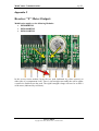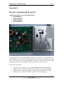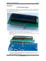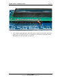
1
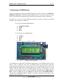
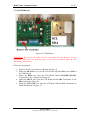
MobiComm© Communications
Page 1
ATV LCD KIT
BlueBoard
User Manual & Technical Reference
May 2009
Version 2.5
MobiComm© Communications
http://www.mobicomm.net/
E-Mail: [email protected]
Tel: +31-70-4041060
The Hague: Forellendaal 245, 2553 JJ, The Hague, Netherlands
Copyright 2005 - 2006, MobiComm© Communications
ATV LCD KIT
Copyright 2005-2009, MobiComm© Communications
MobiComm© Communications
Page 2
Disclaimer
The information contained in this document is believed to be correct and complete.
MobiComm© Communications reserves the right to modify any of the documentation at any
time and without notice. MobiComm© Communications assumes no responsibility for any
infringements of patents or other rights of third parties that may result from the use of any
product or documentation of MobiComm© Communications.
Trademarks
MobiComm and DFM are trademarks of MobiComm© Communications. All other company
and product names are trademark of their respective holders.
Copyright
This document is copyrighted. All rights are reserved.
Copyright © 2005 - 2009 MobiComm© Communications The Hague, Netherlands.
ATV LCD KIT
Copyright 2005-2009, MobiComm© Communications
MobiComm© Communications
Page 3
Table of Contents
INTRODUCTION .........................................................................................................................................5
WELCOME ........................................................................................................................ 5
THE COMPANY ................................................................................................................. 5
1. KIT OVERVIEW ......................................................................................................................................6
OPERATION ...................................................................................................................... 7
1.1 FIRMWARE ................................................................................................................. 8
1.2 PCB ........................................................................................................................... 8
1.3 COMPONENTS ............................................................................................................ 9
2 CONSTRUCTION ...................................................................................................................................10
2.1 LCD DISPLAY.......................................................................................................... 10
2.2 PUTTING THE PCB TOGETHER. ................................................................................ 11
2.2.1 Micro switches ................................................................................................. 11
2.2.2 Capacitors........................................................................................................ 11
2.2.3 Potentiometer................................................................................................... 12
2.2.4 DC Power circuitry.......................................................................................... 12
2.2.5 PIC16F688....................................................................................................... 13
2.2.6 LCD display ..................................................................................................... 13
2.2.7 Contrast adjustment ......................................................................................... 14
3 CONFIGURATION .................................................................................................................................14
3.1 STARTUP SCREEN..................................................................................................... 14
3.2 CONFIGURATION MENU ........................................................................................... 14
3.3 RECEIVER SELECTION .............................................................................................. 15
3.4 TRANSMITTER SELECTION ....................................................................................... 15
3.5 SAVING THE SETTINGS ............................................................................................. 16
3.6 NORMAL OPERATION ............................................................................................... 16
4 NORMAL OPERATION.........................................................................................................................17
4.1 CHANGING THE RECEIVER FREQUENCY ................................................................... 17
4.2 CHANGING THE TRANSMITTER FREQUENCY ............................................................ 18
4.3 RECEIVER SCANNING MODE .................................................................................... 18
5 MENU MODE ..........................................................................................................................................19
5.1 CHANGING THE RECEIVER IF FREQUENCY............................................................... 19
6 CONFIGURATION MODE....................................................................................................................20
7 INTERFACING TO DFM BOARDS .....................................................................................................21
7.1 ALL TSIM BOARDS ................................................................................................. 22
7.2 DFM900TSIM1W & DFM900TSIM2W AND DFM1200TSIM1W(UK) BOARD . 23
7.3 DFM900RTIM & DFM1200RTIM AND DFM1394RTIM BOARD ........................ 24
ATV LCD KIT
Copyright 2005-2009, MobiComm© Communications
MobiComm© Communications
Page 4
7.4 DFM2400RTIM BOARD ......................................................................................... 25
7.5 DFM23500TSIMP BOARD ..................................................................................... 26
APPENDIX A ..............................................................................................................................................27
APPENDIX B...............................................................................................................................................28
APPENDIX C ..............................................................................................................................................29
APPENDIX D ..............................................................................................................................................30
APPENDIX E...............................................................................................................................................31
APPENDIX F...............................................................................................................................................32
ATV LCD KIT
Copyright 2005-2009, MobiComm© Communications
MobiComm© Communications
Page 5
Introduction
Welcome
Congratulations with buying the ATV LCD KIT, we hope you will enjoy building it
and that the LCD KIT will work up to your expectations. We would like to thank you
for buying the product from us, we also would like to ask you to have a look at all our
other products: http://www.mobicomm.net. We have put the most care in putting
this document and KIT together, but if you have problems or a complain regardless of
our efforts you can always contact us direct for assistance and help: e-mail
[email protected]. If you send us an e-mail you should tell in a few clear lines
the kind of problem or complain you have.
The Company
The MobiComm® Communications is a young and dynamic company, founded 1st
June 1999 in The Hague, Netherlands. The company is specialized in the research &
development, production and promotion of innovative mobile communication
technologies in particular but not exclusively for professional mission-critical use.
The company is primarily selling to governmental organizations, defense agencies,
embassies, international relief organizations and international businesses.
ATV LCD KIT
Copyright 2005-2009, MobiComm© Communications
MobiComm© Communications
Page 6
1. KIT Overview
The MobiComm® Communications ATV LCD KIT has been designed with the
greatest care. There are two type of ATV LCD KIT’s a low cost KIT which is
containing only the PCB and a pre-programmed PIC16F688 and the complete KIT.
This KIT is complete and comes with backlight 2 * 16 LCD display, a preprogrammed PIC16F688 high performance 5 MIPS @ 20 MHz 8 bits RISC
microcontroller which is running the embedded universal firmware developed by
MobiComm® Communications. Since the microcontroller is pre-programmed it takes
a lot of complex work out of your hands, making the construction of the LCD KIT
easy and fail proof. For the technical people here some technical features about the
microcontroller and firmware.
•
•
•
•
•
•
•
Firmware written in: Assembler.
Firmware binary code size: 3436 Bytes.
Firmware saves user selected settings and backup copy.
Microcontroller speed: 2 MIPS @ 8 MHz.
PIC16F688 High performance 8 bits RISC.
10 Bits A/D converter.
256 Bytes EEPROM.
ATV LCD Controller for Comtech Modules
This Product will allow the control of Comtech transmit and receiver modules,
it may also control modules from other manufacturers which use the
TSA5055 or SP5055 PLL I/Cs.
Features
•
Smart up/down tuning
•
Receiver Scan Mode (Up/Down or Sweep Scanning)
•
250 KHz channel spacing
•
Bar graph "S" meter
•
PTT with on-board transmit 2A power switch
•
13, 23 and 33 cm operation with the same software*
•
Receiver or Transmitter only function*
* By configuration menu selection
ATV LCD KIT
Copyright 2005-2009, MobiComm© Communications
MobiComm© Communications
Page 7
Operation
This unit's functionality can be best appreciated from a description of its operation.
Normally only the receive frequency including the S-Meter is displayed, a "*" symbol
in the right hand column points to the line which can currently be controlled by the
UP/DOWN keys. Receive frequency and IF frequency is display on the top line
transmit on bottom, there are 5 press buttons which function as follows:
UP
Pressing the UP button will increase the frequency displayed and market by the “*”
symbol. Normally the frequency increments are 250 KHz but if you press the key
continuously the frequency increments will slowly increase to 2 MHz, resulting in a
tuning speed of 10 MHz/sec. Pressing the UP and DOWN buttons at the same time for
a prolonged period will activate the Receiver Scan Mode, pressing the SELECT
button will deactivate this mode. The mode is automatically ended when a Station is
detected.
DOWN
Pressing the DOWN button will decrease the frequency displayed and market by the
“*” symbol. Normally the frequency decrements are 250 KHz but if you press the key
continuously the frequency decrements will slowly increase to 2 MHz, resulting in a
tuning speed of 10 MHz/sec. Pressing the UP and DOWN buttons at the same time for
a prolonged period will activate the Receiver Scan Mode, pressing the SELECT
button will deactivate this mode. The mode is automatically ended when a Station is
detected.
SELECT
Pressing the SELECT button will enable you to select between the top and bottom
line of the LCD display, making it possible to either change receive or transmit
frequency. Pressing the SELECT button for a prolonged period will enable you
change the IF frequency setting of the receiver.
MEM
Pressing the MEM button will directly save all changed settings indicated by an “!”
symbol.
ON/OFF
Pressing the ON/OFF button will switch the 12Volt transmitter power supply ON or
OFF, the LED will indicate if the transmitter is activated.
ATV LCD KIT
Copyright 2005-2009, MobiComm© Communications
MobiComm© Communications
Page 8
1.1 Firmware
The universal firmware has been designed especially for the LCD KIT and can be
used for our entire DFM transmitter and receiver board product range, the user can
select during the configuration phase the type of board and the board combination.
The user selects any transmitter and receiver board combination without any
restrictions on the frequency bands. The user also has to understand that it’s NOT
possible to select two transmitters or two receivers, only a combination of one
transmitter and one receiver.
The selected transmitter and receiver combination can always be changed at a later
moment; there is no restriction1 on the number of times the configuration phase is
started. The firmware uses an intelligent programming algorithm whereby only
modified bytes in EEPROM are programmed, extending EEPROM life span. The
firmware not only saves the selected user settings together with the user selected
transmitter and receiver frequencies but also a backup copy for system crashes that is
detected during boot time.
The backup copy is used to remember the board type combination that was selected
during the configuration. The backup copy will be silently used during boot time
when the 16 bits CRC (Cyclic Redundancy Check) is done on the user EEPROM
settings and failed. The backup copy does not hold the latest user frequency setting
but only the board combination settings that are used to recreate the user EEPROM
settings. A 16 bits CRC is protecting the backup copy when this CRC fails the
firmware will automatically start the configuration phase.
1.2 PCB
The high quality 60 mil flame retardant FR4 based professional PCB with an εr of 4.5
has been produced and designed with the latest technology. The PCB is protected
with an UV protecting anti-solder layer while the solder pad’s are covered with a so
called HAL layer for better soldering capabilities. The PCB has been electrically
tested during production by a nail table; this is a fully automated robot with long thin
contacts that is testing the PCB traces for shorts and interruptions, all PCB’s passed
this test successfully. Figure 1 is giving an overview of the Top and Bottom layer of
the PCB, the user can see that T1 and U2 can be mounted on top or on the bottom of
the PCB to make your life as easy as possible.
1
The only restriction is on the number of times the EEPROM memory can be written, the datasheet is
giving a guaranteed write cycles number of 1,000,000 times.
ATV LCD KIT
Copyright 2005-2009, MobiComm© Communications
MobiComm© Communications
Page 9
Figure 1: Top and Bottom Layer of PCB
1.3 Components
The complete KIT is delivered with all components including the backlight 2 * 16
LCD display, a pre-programmed PIC16F688 high performance RISC microcontroller
which is running the embedded universal firmware developed by MobiComm®
Communications and high quality components including a PCB board. Figure 2 is
giving an overview of all components that are included in the KIT, before you
continue we advice you to check if you can identify all components by using the
component list and Figure 2.
Figure 2: All components
Some Components have changed please check the Component List on Page 10 !.
ATV LCD KIT
Copyright 2005-2009, MobiComm© Communications
MobiComm© Communications
Page 10
Component List 2009:
•
•
•
•
•
•
•
•
•
•
•
•
•
•
•
•
•
•
•
•
•
•
U1
U2
R1
R5
R2
R2
R4 & R6
R7 & R8:
R9
C1 – C3:
C4
J1
J2
J3
J4
J5
J6
S1 – S5
D1
D2 – D5
T1
T2
: PIC16F688 + 14pin socket.
: UA7805
: 3K3
: 330 Ohm
: 4.7 Ohm. (Delivered with Green-Yellow LCD display)
: 10 Ohm (Delivered with Blue-White LCD display)
: 10K potentiometer.
: 33K.
: 10K.
: 100nF.
: 220uF/25 V Capacitor.
: 4pin header.
: Optional header for external LCD display (not included)
: 2 * 16 LCD Display + 16pin header.
: Optional 5pin header for external KeyBoard (not included).
: DC Power Jack 2.5mm.
: 4pin header.
: Micro Switches.
: Red 3 mm LED.
: 3K3 1/8w (Signal Diodes have been replaced with 3K3).
: IRF 9610 (Power P-MOSFET 2A/200V).
: BC547C or 2N3904 (Signal NPN Transistor).
2 Construction
You should start by placing all components in front of you and make sure you can
identify them from the above list and Figure 2. You need the following tools to
complete the construction of the LCD KIT in a proper and fast manner.
•
•
•
•
Soldering ion (15 – 40 Watts).
Wire stripper.
Wire cutter.
Solder wire.
2.1 LCD Display
We will start by putting the LCD display and 16 pin header together; the short pins
should be connected to the display side as can be seen in Figure 3.
PLEASE CHECK APPENDIX F FOR THE DISPLAY !.
Figure 3: Display connected to 16 pin header.
ATV LCD KIT
Copyright 2005-2009, MobiComm© Communications
MobiComm© Communications
Page 11
2.2 Putting the PCB together.
Best is to place first the normal resistors on the PCB board, R1, R2, R3, R5, R7 up-to
R9 can clearly be identified on the PCB. Use the component list from Page 10 to
check which resistor value should be put on the PCB. After the resistors have been
placed on the PCB you should solder them and remove the long wires using the wire
cutter tool. The resistors D2 up-to D5 should be placed; they are 3K3 and 1/8w type
(small type). They use to be small signal diodes but have been replaced with 3K3, on
the photo’s you can still clearly see the signal diodes. NOTE: Do not use signal
diodes since the software is expecting resistors!.
2.2.1 Micro switches
The next step is placing the 5 micro switches, be careful when you do this since you
don’t want to hurt yourself. Best is to place the micro switches in their position and by
using both thumbs to press them through the PCB board. After the micro switches
have been placed and soldered you can place the 14 pin IC socket, look carefully for
the position of U2 and the notch on the IC socket and the place of the notch on the
PCB board.
2.2.2 Capacitors
Now its time for placing the 100nF capacitors, C1..C3, the capacitors should be
placed at the printed side of the PCB. Place the capacitors Figure 4, as close as
possible to the PCB since the LCD display will be mounted on top of the capacitors.
Figure 4: 100nF Capacitor.
The Electrolytic capacitor C4 the 220uF /25 V, Figure 5 should be placed now; check
the negative marking on the capacitor and the long wire is positive. This should match
the (+) plus sign marking on the PCB.
Figure 5: 220uF Electrolytic capacitor.
ATV LCD KIT
Copyright 2005-2009, MobiComm© Communications
Page 12
MobiComm© Communications
2.2.3 Potentiometer
The next step is to place the remaining components on the PCB board; we start with
R4 and R6 the 10K potentiometers. The R4 potentiometer is used to control the
contrast on the LCD display. While the R5 potentiometer can be used to control the
output voltage of the 2A power MOSFET switch. This is handy if you want to control
output power of a PA.
2.2.4 DC Power circuitry
We need to place the voltage regulator U2, market as UA7805, look at Figure 6 to see
how the regulator U2 should be placed.
Figure 6: Position of U2 and T1.
The PCB is ready to have the U2 placed at the top or at the bottom of the PCB, if you
place the LCD display on the top of the PCB you will have to place U2 and T1 at the
bottom. Bend the pins and make sure it can be mounted with the M3 nut and bold
supplied. The power MOSFET T1 needs to be placed on the same side, as the voltage
regulator U2 is careful since this component is static sensitive.
Bend the pins and make sure it can be mounted with the M3 nut and bold supplied.
Don’t forget to place the transistor T2.
The DC Power Jack J5 connector should be place next to capacitor C4; it does not
need an explanation how this should be placed since it can only be placed in one way.
The external connections with the receiver or transmitter boards can be done through
J1 (receiver) and J6 (transmitter). We have supplied connection pins for this but if you
want to connect wires directly on the board its also fine.
ATV LCD KIT
Copyright 2005-2009, MobiComm© Communications
Page 13
MobiComm© Communications
The last component we need to place is the red 3mm LED, the LED has a long and a
short pin. The short pin should go through the hole in the PCB closest to the LCD
display, the long pin (+) should go in the opposite hole that is closest to the marker R7
on the PCB.
2.2.5 PIC16F688
We now need to place the brains, in our case the pre-programmed PIC16F688, in the
IC socket that you have placed before. Look carefully for the notch in the PIC16F688
enclosure and bend the pins if needed to put it gently in the 14 pin IC socket. The
notch in the enclosure should match with the notch in the IC socket. Do this with care
and don’t rush things. Keep in mind that the chip is sensitive to static electricity and
that a good working bench is required to do things properly.
2.2.6 LCD display
To complete the construction process you need to place the LCD display with the 16pin header that we soldered before. After you have placed the LCD display and
soldered it you should use a wire cutter to remove any excess of pin length from the
header.
You’re now done and the PCB should now look like the picture in Figure 7. If you
have a different result you should re-check all the steps and correct the error.
Figure 7: The completed PCB Board.
Some Components have changed please check the Component List on Page 10 !.
ATV LCD KIT
Copyright 2005-2009, MobiComm© Communications
Page 14
MobiComm© Communications
2.2.7 Contrast adjustment
Before we connect the board to a regulated 12 Volt power supply with a center pin +
signal we have to set R4, the LCD contrast control correct. The best is to put the
contrast control potentiometer R4 in the same position as can be seen in Figure 7.
This is close to the 4 O’clock setting if the board has the same orientation as in Figure
7.
3 Configuration
3.1 Startup Screen
Connect the board to a regulated 12 Volt power supply with a center pin +, the power
supply should be able to deliver some 500mA – 1000mA depending on the type of
boards you would like to control. The LCD board has a current consumption of about
120mA @ 12 Volt.
Figure 8: Startup Screen.
The startup screen will always be visible during the first couple of seconds after
power is applied to the board. During this time the firmware is checking if the stored
information in EEPROM is having a valid CRC and preparing for loading them in
SRAM for later use. The firmware also checks if the configuration menu or normal
operation mode should be started.
3.2 Configuration Menu
When power is applied for the first time after you completed the KIT the firmware
will always start the configuration menu. The configuration menu will look like the
picture in Figure 9.
Figure 9: Configuration Menu.
ATV LCD KIT
Copyright 2005-2009, MobiComm© Communications
Page 15
MobiComm© Communications
The “*” market behind the text line is indicating on which line the UP/DOWN keys
have an effect. At startup this will always be the Receiver list. With the UP/DOWN
keys we now can select the Receiver board you would like to control form the list, if
no receiver will be attached you should always select the NONE setting.
3.3 Receiver Selection
In our example, see Figure 10, we selected the DFM2400RTIM receiver board; this
board can receive from 2300 up-to 2600 MHz as can be seen from Appendix A.
Figure 10: Receiver Board Selection.
With the SELECT key you can switch between the Receiver and Transmitter board
list, you will see that the “*” market behind the text line will also change accordingly
as can be seen in Figure 11.
Figure 11: Transmitter Board List.
3.4 Transmitter Selection
In our example, see Figure 12, we will select the DFM1200TSIM 70mW transmitter
from the list, this transmitter has an frequency range of 1100 up-to 1600 MHz as can
be seen from Appendix A.
Figure 12: Transmitter Board Selection.
ATV LCD KIT
Copyright 2005-2009, MobiComm© Communications
Page 16
MobiComm© Communications
3.5 Saving the Settings
If you have changed the Receiver and or Transmitter board you will see an “!”
exclamation market at the end of the line indicating that the new settings have not
been saved to EEPROM memory. When you are happy with the selected boards you
should always save the settings by pressing the MEM key, almost directly you will
see the exclamation markers disappear, see Figure 13. This is an indication that the
selected settings have been saved in EEPROM memory and that a backup copy has
been made and saved in case of system crashes.
Figure 13: Settings saved in EEPROM memory.
If you’re not happy with the settings you can still change them and save them again
and again, there is no limitation on the number of times they are changed and/or
saved. Even in a later stage when you purchased a receiver or transmitter you can still
add the receiver or transmitter control to your settings.
3.6 Normal Operation
If you’re done you can remove the power from the board and re-connect the power to
reset the boards Firmware. The startup screen will first be visible but soon after that
the normal mode screen will be visible as can be seen from Figure 14.
Figure 14: Receiver Mode.
If you selected only a Transmitter board and Receiver board was set at NONE the
startup screen will look a little bit different but you will recognize it clearly. Since we
selected both a Transmitter and Receiver board we will have this startup screen, other
Receiver and or Transmitter board combinations will give different results.
ATV LCD KIT
Copyright 2005-2009, MobiComm© Communications
Page 17
MobiComm© Communications
Figure 15: Transmitter Mode.
With the SELECT key you can switch between the Receiver and Transmitter boards
just like during the configuration, you will again see that the “*” market behind the
text line will also change accordingly as can be seen in Figure 15.
The UP/DOWN keys can be used to change the Frequency of the Receiver and/or
Transmitter depending on which line the “*” marker is displayed. Saving the changed
frequency settings can again be done by the MEM key.
4 Normal Operation
4.1 Changing the Receiver Frequency
The Receiver frequency can be changed by pressing the UP/DOWN keys while the
“*” marker is displayed on the top line of the display, as can be seen from Figure 16.
Figure 16: Receiver Mode.
The bar below the receiver frequency is the S-Meter or also known as Signal strength
meter. If you connected the S-Meter input of the board to your Receiver S-Meter
output you can see a bar like this one, depending on the fact if a strong signal is
received or not.
If you have changed the frequency you will see an “!” exclamation marker at the end
of the line indicating that the new settings have not been saved to EEPROM memory.
If you want the next time you power up the board it comes back to this frequency you
should press the MEM key, almost directly you will see the exclamation marker(s)
disappear, and the settings are saved in EEPROM..
ATV LCD KIT
Copyright 2005-2009, MobiComm© Communications
Page 18
MobiComm© Communications
4.2 Changing the Transmitter Frequency
Just as with the Receiver frequency can you change the Transmitter frequency by
pressing the UP/DOWN keys while the “*” marker is displayed on the bottom line of
the display, as can be seen from Figure 17.
Figure 17: Transmitter Mode.
With the SELECT key you can switch between the Receiver and Transmitter boards
just like during the configuration, you will again see that the “*” market behind the
text line will also change accordingly as can be seen in Figure 17.
If you have changed the frequency you will see an “!” exclamation market at the end
of the line indicating that the new settings have not been saved to EEPROM memory.
If you want the next time you power up the board it comes back to this frequency you
should press the MEM key, almost directly you will see the exclamation marker(s)
disappear, and the settings are saved in EEPROM..
Its important to realize that by pressing the MEM key, not only the changes made to
the line the “*” marker is saved but all changes made are saved.
4.3 Receiver Scanning Mode
The Receiver Scanning Mode can be activated by pressing the UP and DOWN keys
at the same time for a prolonged period while the “*” marker is displayed on the top
line of the display, as can be seen from Figure 16. The Scanning Mode will now start
to search for an RF signal, scanning is not based on signal level but on the presents of
a carrier that will be captured by the Video Demodulation PLL chip inside the Tuner
Module.
When the Receiver Scanning Mode is activated with UP/DOWN key press the Sweep
Scanning Mode is activated. The Frequency increases or decreases based on the last
direction pressed before the Scan Mode was activated, at the end of the band the
Scanning changes direction and continues until a carrier is detected. The scanning
direction can be changed during this mode by simply pressing UP or DOWN keys,
this will also switch the Sweep Scanning Mode into Normal Scanning Mode.
Receiver Scanning Mode is deactivate by pressing the SELECT key or if the presents
of a carrier is detected.
ATV LCD KIT
Copyright 2005-2009, MobiComm© Communications
Page 19
MobiComm© Communications
5 Menu Mode
The Menu Mode is activated by pressing the SELECT key for more than 2 seconds,
when you do this the screen from Figure 18 will be displayed.
Figure 18: Menu Mode.
5.1 Changing the Receiver IF Frequency
Normally this is not needed but if you like your receiver to be 100% correctly
indicating the Receiver frequency you need to be able to change the IF frequency. The
Receiver IF frequency is about 479.50 MHz, I say “about” with a very good reason.
The IF frequency of the tuner module is determined by a SAW filter, the exact
frequency can be different from the 479.50 MHz, the frequency error can be as much
as 2 MHz which is small compared to the receiver bandwidth of 18 or 27 MHz, but
still there is an error that should be compensated for to make sure the displayed
frequency matches the one transmitted by the transmitting station. For this reason you
can change and save the Receiver IF frequency in the Menu Mode, see Figure 18. The
IF frequency can be changed by pressing the UP or DOWN keys while the “*”
marker is displayed on the top line of the display. Changing the IF frequency does not
really change the IF frequency since it is determined by the SAW filter but the
frequency error on the display is corrected. By pressing the MEM key the changed IF
frequency can be saved. You can exit the Menu Mode by pressing the SELECT key
for more than two seconds.
ATV LCD KIT
Copyright 2005-2009, MobiComm© Communications
Page 20
MobiComm© Communications
6 Configuration Mode
When power was applied for the first time after you completed the KIT the firmware
started the configuration menu automatically, but what if you want to change
something at a later moment and you need to get access again to the configuration
menu?. The following procedure should be followed to start the configuration menu.
WARNING: All previously saved settings will be lost including the Receiver IF
frequency setting. If needed you should write the settings down on a paper before
continuing the configuration mode.
1.
2.
3.
4.
Remove power from the LCD board.
Press the UP and DOWN key at the same time.
Re-apply the power back to the LCD board while pressing all the keys from 2.
Wait until you see the startup screen from Figure 19, you can now stop pressing the
keys.
Figure 19: Startup Screen.
After a few seconds you will see the configuration menu like in Figure 20.
Figure 20: Configuration Menu.
A detailed explanation on how to configure the LCD board can be found in chapter 3
Configuration
ATV LCD KIT
Copyright 2005-2009, MobiComm© Communications
Page 21
MobiComm© Communications
7 Interfacing to DFM Boards
Before you continue interfacing the DFM board(s) to your LCD board you NEED TO
REMOVE THE PIC controller from the DFM board. If you don’t it will not work
and it’s possible that you harm the PIC16F688 microcontroller on the LCD Board.
In Figure 21 you can see all the different interfaces you have to make to the DFM
board(s). The interfaces are labeled:
J6: For the Transmitter DFM Board:
1.
2.
3.
4.
POWER SUPPLY
GND
SCL
SDA
J1: For the Receiver DFM Board:
1.
2.
3.
4.
S-Meter
GND
SDA
SCL
Figure 21: LCD Board.
You should now connect the LCD Board connections to your DFM board(s) of your
choice. This is relatively easy since all DFM boards are listed below with the
interfaces labeled that need to be connected to the corresponding labels on the LCD
Board. Read the instructions carefully and take your time for the work. Use good
quality electrical cable between the DFM board(s) and the LCD Board, its good
practice to use different colors to avoid confusion. Use BLACK for GND, Blue for
SDA, Yellow for SCL, Green for S-Meter and finally Red for POWER SUPPLY.
The Receiver POWER SUPPLY should be directly connected to the same power
supply as the LCD Board.
ATV LCD KIT
Copyright 2005-2009, MobiComm© Communications
Page 22
MobiComm© Communications
7.1 All TSIM Boards
Figure 22: TSIM Board.
WARNING: Do not use the SDA & SCL connections for the Receiver for the
Transmitter since they are different, that is why they are labeled SDA & SCL
Transmitter and Receiver.
Follow the instructions:
1. Remove the PIC Controller as indicated in Figure 22.
2. Solder the BLACK wire from the LCD Board labeled GND to the GND of
the TSIM Board.
3. Solder the RED wire from the LCD Board labeled POWER SUPPLY
Transmitter to the + indicated in Figure 22.
4. Solder the BLUE wire from the LCD Board labeled SDA Transmitter to the
SDA indicated in Figure 22.
5. Solder the YELLOW wire from the LCD Board labeled SCL Transmitter to
the SCL indicated in Figure 22.
ATV LCD KIT
Copyright 2005-2009, MobiComm© Communications
Page 23
MobiComm© Communications
7.2 DFM900TSIM1W & DFM900TSIM2W and DFM1200TSIM1W(UK) Board
Figure 23: DFM1200TSIM1W Board.
Figure 24: Detailed view DFM1200TSIM1W Board.
WARNING: Do not use the SDA & SCL connections for the Receiver for the
Transmitter since they are different, that is why they are labeled SDA & SCL
Transmitter and Receiver.
Follow the instructions:
1. Remove the PIC Controller as indicated in Figure 24.
2. Solder the BLACK wire from the LCD Board labeled GND to the GND of
the TSIM1W Board, indicated in Figure 23.
3. Solder the RED wire from the LCD Board labeled POWER SUPPLY
Transmitter to the + indicated in Figure 23.
4. Solder the BLUE wire from the LCD Board labeled SDA Transmitter to the
SDA indicated in Figure 24.
5. Solder the YELLOW wire from the LCD Board labeled SCL Transmitter to
the SCL indicated in Figure 24.
NOTE: The wire color can change, please check the position of the wire !.
ATV LCD KIT
Copyright 2005-2009, MobiComm© Communications
Page 24
MobiComm© Communications
7.3 DFM900RTIM & DFM1200RTIM and DFM1394RTIM Board
Figure 25: 900, 1200 and 1394RTIM Board.
WARNING: Do not use the SDA & SCL connections for the Transmitter for the
Receiver since they are different, that is why they are labeled SDA & SCL
Transmitter and Receiver.
The Receiver POWER SUPPLY should be directly connected to the same power
supply as the LCD Board.
Follow the instructions:
1. Remove the PIC Controller as indicated in Figure 25.
2. Solder the BLACK wire from the LCD Board labeled GND to the GND of
the RTIM Board, indicated in Figure 25.
3. Solder the RED wire from the LCD Board labeled POWER SUPPLY
Receiver to the + indicated in Figure 25.
4. Solder the BLUE wire from the LCD Board labeled SDA Receiver to the SDA
indicated in Figure 25.
5. Solder the YELLOW wire from the LCD Board labeled SCL Receiver to the
SCL indicated in Figure 25.
6. Solder the GREEN wire from the LCD Board labeled S-Meter Receiver to
the S-Meter indicated in Figure 25. See also the NOTE below.
NOTE: Before you can use the S-Meter on the DFM900, 1200 or 1394RTIM Boards
you need to make the modification explained in Appendix C of this document.
NOTE: Before you can use the Scanning Mode on the DFM900, 1200 or 1394RTIM
Boards you need to make the connections and modification explained in Appendix D
and E of this document.
ATV LCD KIT
Copyright 2005-2009, MobiComm© Communications
Page 25
MobiComm© Communications
7.4 DFM2400RTIM Board
Figure 26: DFM2400RTIM Board.
WARNING: Do not use the SDA & SCL connections for the Transmitter for the
Receiver since they are different, that is why they are labeled SDA & SCL
Transmitter and Receiver.
The Receiver POWER SUPPLY should be directly connected to the same power
supply as the LCD Board
Follow the instructions:
1. Remove the PIC Controller as indicated in Figure 26.
2. Solder the BLACK wire from the LCD Board labeled GND to the GND of
the RTIM Board, indicated in Figure 26.
3. Solder the RED wire from the LCD Board labeled POWER SUPPLY
Receiver to the + indicated in Figure 26.
4. Solder the BLUE wire from the LCD Board labeled SDA Receiver to the SDA
indicated in Figure 26.
5. Solder the YELLOW wire from the LCD Board labeled SCL Receiver to the
SCL indicated in Figure 26.
6. Solder the GREEN wire from the LCD Board labeled S-Meter Receiver to
the S-Meter indicated in Figure 26.
NOTE: Before you can use the Scanning Mode on the DFM2400RTIM Board you
need to make the connections explained in Appendix D of this document.
ATV LCD KIT
Copyright 2005-2009, MobiComm© Communications
Page 26
MobiComm© Communications
7.5 DFM23500TSIMP Board
Figure 27: DFM24350TSIMP Board.
WARNING: Do not use the SDA & SCL connections for the Receiver for the
Transmitter since they are different, that is why they are labeled SDA & SCL
Transmitter and Receiver.
The Transmitter POWER SUPPLY should be directly connected to the same power
supply as the LCD Board
Follow the instructions:
1. Remove the PIC Controller as indicated in Figure 27.
2. Solder the BLACK wire from the LCD Board labeled GND to the GND of
the TSIM1W Board, indicated in Figure 27.
3. Solder the RED wire from the LCD Board labeled POWER SUPPLY
Transmitter to the + indicated in Figure 27.
4. Solder the BLUE wire from the LCD Board labeled SDA Transmitter to the
SDA indicated in Figure 27 (Pin 1 PIC).
5. Solder the YELLOW wire from the LCD Board labeled SCL Transmitter to
the SCL indicated in Figure 27 (Pin 2 PIC).
ATV LCD KIT
Copyright 2005-2009, MobiComm© Communications
Page 27
MobiComm© Communications
Appendix A
Technical specifications:
DFM900TSIM
DFM900TSIM1W
DFM900TSIM2W
DFM1080TSIM1W
DFM1200TSIM
DFM1200TSIM1W
DFM1200TSIM1WUK
DFM1394TSIM
DFM2350TSIMP
DFM2400TSIM
DFM2400TSIMP
850 - 1000 MHz
900 - 1000 MHz
900 - 1000 MHz
1100 - 1300 MHz
1100 - 1600 MHz
1100 - 1300 MHz
1100 - 1325 MHz
1150 - 1600 MHz
2300 - 2600 MHz
2300 - 2600 MHz
2300 - 2600 MHz
DFM900RTIM
DFM1200RTIM
DFM1394RTIM
DFM2400RTIM
850 - 1000 MHz
1100 - 1800 MHz
1150 - 1800 MHz
2300 - 2600 MHz
Signal Strength Meter
Tuning Step (Normal)
Tuning Step (Fast)
Tuning Speed (Normal)
Tuning Speed (Fast)
:
:
:
:
:
Yes
250 KHz
2 MHz
2 MHz/s
10 MHz/s
ATV LCD KIT
Copyright 2005-2009, MobiComm© Communications
Page 28
MobiComm© Communications
Appendix B
ATV LCD KIT
Copyright 2005-2009, MobiComm© Communications
Page 29
MobiComm© Communications
Appendix C
Receiver "S" Meter Output:
Modification applies to the following Modules:
• DFM900RTIM
• DFM1200RTIM
• DFM1394RTIM
In the receiver tuner module, locate the two pads (indicated by yellow arrows) on
either side of a compartment 'wall'. There is just enough room under the wall to solder
a small wire link between the pads. The signal strength voltage will now be on PIN 9
of the tuner (indicated by red arrow).
ATV LCD KIT
Copyright 2005-2009, MobiComm© Communications
Page 30
MobiComm© Communications
Appendix D
Receiver Scanning Mode mod 1:
Modification applies to the following Modules:
• DFM900RTIM
• DFM1200RTIM
• DFM1394RTIM
• DFM2400RTIM
To make the Receiver Scanning Mode work two wires have to be connected to the
Tuner Module. For All types of Tuner Modules the wires are connected to the same
pins !. The Purple wire on the Photograph is connected to PIN 9, the signal strength
voltage output on the Tuner Module, and serves here as a reference point..
Follow the instructions:
1.
2.
3.
4.
Take two wires of about 3 cm (1.2 Inch) length and strip and solder them.
Solder one wire to the PIN 8 and one wire to PIN 10 on the Tuner Module.
Solder the wire connected to PIN 8 to PIN 13 next to the SDA/SCL PINS.
Solder the wire connected to PIN 13 to PIN 5 next to the big gap.
ATV LCD KIT
Copyright 2005-2009, MobiComm© Communications
Page 31
MobiComm© Communications
Appendix E
Receiver Scanning Mode mod 2:
Modification applies to the following Modules:
•
•
DFM900RTIM
DFM1200RTIM
• DFM1394RTIM
In the receiver tuner module, locate the two pads (indicated by yellow arrow) next to
the TA8804F Video Demodulator. There is just enough room to solder a small wire
link or SMD 0603 resistor of 100 Ohm between the pads. The ATF signal voltage will
now be on pin 5 of the tuner.
ATV LCD KIT
Copyright 2005-2009, MobiComm© Communications
Page 32
MobiComm© Communications
Appendix F
LCD Backlight Display
The new high quality display we are now using does have PIN 15 and PIN 16
reversed with what we are expecting, that is why two small wires are needed to make
the backlight work as expected.
1. Solder the header onto the display and leave PIN 15 and PIN 16 open, pin
numbering is visible on the back of the LCD display board !.
2. Solder two wires of about 2 cm (0.8 Inch) on PIN 15 and PIN 16 as in the
above picture.
3. Place the LCD Display like on the above picture and solder the two wires. Do
this only after all other components have been placed. In the picture we did
not do this to make it more clear.
ATV LCD KIT
Copyright 2005-2009, MobiComm© Communications
Page 33
MobiComm© Communications
4. Now turn the board and place the header above the holes and solder the header
to the ATV LCD KIT PCB. PIN 15 and PIN 16 will now be swapped and the
Backlight will work normally as expected.
ATV LCD KIT
Copyright 2005-2009, MobiComm© Communications