1
UM1553
User manual
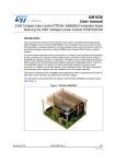
STEVAL-IHM034V2 dual motor control and PFC demonstration
board featuring the STM32F103RC and STGIPS20C60
Introduction
The STEVAL-IHM034V2 is a complete motor control kit solution, for the evaluation of
STMicroelectronics wide product portfolio targeted at applications where it is necessary to
simultaneously drive two motors in sensorless field oriented control (FOC) and perform
active power factor correction (PFC) through digital control of a single-stage boost DC-DC
converter. Typical application is in room air conditioners (RACs), where this solution can
drive the compressor, the outdoor fan, and the PFC.
The microcontroller unit is the STMicroelectronics ARM™ Cortex-M3 core-based
STM32F103RC, which is able to simultaneously carry out all the above mentioned tasks.
The board is compatible for use with the STM32F2 series, and with the ARM™ Cortex-M4
core-based STM32F4 series.
Motor 1 is powered by the onboard SLLIMM™ (small low-loss intelligent molded module)
STGIPS20C60; motor 2 can be powered by an external STMicroelectronics power stage,
such as those that can be evaluated by means of the STEVAL-IHM021V2, STEVALIHM024V1, STEVAL-IHM032V1, or STEVAL-IHM035V2.
Simultaneously, the same microcontroller unit drives the onboard boost PFC stage,
designed with the STGW35HF60W ultrafast IGBT and the STTH15R06 Turbo2 ultrafast
diode.
The STEVAL-IHM034V2 can be used together with the STM32 permanent magnet
synchronous motors (PMSM) single/dual FOC software development kit (SDK) v3.2, and
successive versions, and its compatible PFC firmware v1.0 plug-in, and successive
versions. This user manual provides information on using the STEVAL-IHM034V2 board
and its hardware features.
Figure 1. Image
December 2013
DocID023347 Rev 2
1/52
www.st.com
Contents
UM1553
Contents
1
System introduction . . . . . . . . . . . . . . . . . . . . . . . . . . . . . . . . . . . . . . . . . 4
1.1
2
3
Target application . . . . . . . . . . . . . . . . . . . . . . . . . . . . . . . . . . . . . . . . . . . . 4
Safety and operating instructions . . . . . . . . . . . . . . . . . . . . . . . . . . . . . . 5
2.1
Demonstration board intended use . . . . . . . . . . . . . . . . . . . . . . . . . . . . . . 5
2.2
Demonstration board installation . . . . . . . . . . . . . . . . . . . . . . . . . . . . . . . . 5
2.3
Electrical connections . . . . . . . . . . . . . . . . . . . . . . . . . . . . . . . . . . . . . . . . . 6
2.4
Microcontroller programming . . . . . . . . . . . . . . . . . . . . . . . . . . . . . . . . . . . 6
Board description . . . . . . . . . . . . . . . . . . . . . . . . . . . . . . . . . . . . . . . . . . . 7
3.1
System architecture . . . . . . . . . . . . . . . . . . . . . . . . . . . . . . . . . . . . . . . . . . 7
3.2
Board schematic . . . . . . . . . . . . . . . . . . . . . . . . . . . . . . . . . . . . . . . . . . . . . 8
4
Connector placement . . . . . . . . . . . . . . . . . . . . . . . . . . . . . . . . . . . . . . . 17
5
Description of jumpers, test pins and connectors . . . . . . . . . . . . . . . . 18
6
STM32 pinout . . . . . . . . . . . . . . . . . . . . . . . . . . . . . . . . . . . . . . . . . . . . . . 21
6.1
7
Configuration for STM32F2 and STM32F4 series . . . . . . . . . . . . . . . . . . 22
Hardware settings / configuration . . . . . . . . . . . . . . . . . . . . . . . . . . . . . 23
7.1
Motor 1, phase current amplification network . . . . . . . . . . . . . . . . . . . . . . 23
7.2
Motor 1, overcurrent protection network . . . . . . . . . . . . . . . . . . . . . . . . . . 25
7.3
PFC stage, mains current amplification network . . . . . . . . . . . . . . . . . . . 25
7.4
PFC stage, overcurrent protection . . . . . . . . . . . . . . . . . . . . . . . . . . . . . . 27
7.5
Single motor configuration . . . . . . . . . . . . . . . . . . . . . . . . . . . . . . . . . . . . 28
7.6
Dual motor configuration . . . . . . . . . . . . . . . . . . . . . . . . . . . . . . . . . . . . . 28
7.7
Dual motor and PFC configuration . . . . . . . . . . . . . . . . . . . . . . . . . . . . . . 29
7.8
PFC configuration . . . . . . . . . . . . . . . . . . . . . . . . . . . . . . . . . . . . . . . . . . . 31
8
Firmware configuration for STM32 PMSM FOC SDK . . . . . . . . . . . . . . 32
9
References . . . . . . . . . . . . . . . . . . . . . . . . . . . . . . . . . . . . . . . . . . . . . . . . 50
2/52
DocID023347 Rev 2
UM1553
10
Contents
Revision history . . . . . . . . . . . . . . . . . . . . . . . . . . . . . . . . . . . . . . . . . . . 51
DocID023347 Rev 2
3/52
52
List of figures
UM1553
List of figures
Figure 1.
Figure 2.
Figure 3.
Figure 4.
Figure 5.
Figure 6.
Figure 7.
Figure 8.
Figure 9.
Figure 10.
Figure 11.
Figure 12.
Figure 13.
Figure 14.
Figure 15.
Figure 16.
Figure 17.
Figure 18.
4/52
Image . . . . . . . . . . . . . . . . . . . . . . . . . . . . . . . . . . . . . . . . . . . . . . . . . . . . . . . . . . . . . . . . . . 1
Board architecture . . . . . . . . . . . . . . . . . . . . . . . . . . . . . . . . . . . . . . . . . . . . . . . . . . . . . . . . 8
Schematic (1 of 9). . . . . . . . . . . . . . . . . . . . . . . . . . . . . . . . . . . . . . . . . . . . . . . . . . . . . . . . . 9
Schematic (2 of 9). . . . . . . . . . . . . . . . . . . . . . . . . . . . . . . . . . . . . . . . . . . . . . . . . . . . . . . . 10
Schematic (3 of 9). . . . . . . . . . . . . . . . . . . . . . . . . . . . . . . . . . . . . . . . . . . . . . . . . . . . . . . . 11
Schematic (4 of 9). . . . . . . . . . . . . . . . . . . . . . . . . . . . . . . . . . . . . . . . . . . . . . . . . . . . . . . . 12
Schematic (5 of 9). . . . . . . . . . . . . . . . . . . . . . . . . . . . . . . . . . . . . . . . . . . . . . . . . . . . . . . . 13
Schematic (6 of 9). . . . . . . . . . . . . . . . . . . . . . . . . . . . . . . . . . . . . . . . . . . . . . . . . . . . . . . . 14
Schematic (7 of 9). . . . . . . . . . . . . . . . . . . . . . . . . . . . . . . . . . . . . . . . . . . . . . . . . . . . . . . . 15
Schematic (8 of 9). . . . . . . . . . . . . . . . . . . . . . . . . . . . . . . . . . . . . . . . . . . . . . . . . . . . . . . . 16
Schematic (9 of 9). . . . . . . . . . . . . . . . . . . . . . . . . . . . . . . . . . . . . . . . . . . . . . . . . . . . . . . . 17
Connector placement . . . . . . . . . . . . . . . . . . . . . . . . . . . . . . . . . . . . . . . . . . . . . . . . . . . . . 18
Motor current measurement, amplification network . . . . . . . . . . . . . . . . . . . . . . . . . . . . . . 24
Motor 1 overcurrent protection network . . . . . . . . . . . . . . . . . . . . . . . . . . . . . . . . . . . . . . . 26
PFC current measurement amplification network . . . . . . . . . . . . . . . . . . . . . . . . . . . . . . . . 27
PFC overcurrent protection network . . . . . . . . . . . . . . . . . . . . . . . . . . . . . . . . . . . . . . . . . . 28
Technical sheet of PFC inductor (page 1 of 2) . . . . . . . . . . . . . . . . . . . . . . . . . . . . . . . . . . 48
Technical sheet of PFC inductor (page 2 of 2) . . . . . . . . . . . . . . . . . . . . . . . . . . . . . . . . . . 49
DocID023347 Rev 2
UM1553
1
System introduction
System introduction
Nominal power: 1300 W, max. power 1700 W
Digital PFC section:
–
Single-stage boost converter
–
STGW35HF60WD ultrafast IGBT in TO-247 package; it may be replaced with an
STGW35HF60W if a free-wheeling diode (like the STTH2L06) is soldered on
between its collector and emitter
–
Turbo2 ultrafast diode STTH15R06D in TO-220AC package
–
AC mains current sensing (shunt resistor and amplification, using rail-to-rail
input/output 8 MHz TSV914)
–
DC bus voltage sensing
–
Hardware overcurrent protection
–
Hardware overvoltage protection
–
AC mains voltage zero crossing detection
–
Rectified AC mains voltage sensing
–
External boost inductor
Inverter section (motor 1 drive):
–
IGBT intelligent power module STGIPS20C60 in SDIP 25L molded package
–
3-shunt or DC link motor current sensing (shunt resistor and amplification, using
rail-to-rail input/output 8 MHz TSV914)
–
Hardware overcurrent protection
–
Heatsink temperature measurement
–
Overcurrent protection disabling network
Control section:
–
Centralized dual motor control and PFC drive, using STM32F103RCT6
–
MC connector to drive the second motor power stage (a compatible power board,
such as STEVAL-IHM021V2, STEVAL-IHM024V1, or STEVAL-IHM032V1, can be
plugged here)
–
SWD programming and debugging
–
JTAG programming (DC +5 V supply only, see Section 2.4)
–
USART communication using ST3232C, insulated with optocouplers;
–
Other functions: user key, reset, potentiometer, user LED, NTC relay, test points
Power supply:
–
1.1
+15 V, +3.3 V power supply based on VIPER16, L78L33AC, LD1117S33TR.
Target application
Air conditioning motor drive (compressor, outdoor fan) and PFC.
DocID023347 Rev 2
5/52
52
Safety and operating instructions
2
UM1553
Safety and operating instructions
Warning:
During assembly, testing, and normal operation, the
demonstration board poses several inherent hazards,
including bare wires, moving or rotating parts, and hot
surfaces. There is a danger of serious personal injury and
damage to property if the kit or components are improperly
used or installed incorrectly. The kit is not electrically
isolated from the AC/DC input. The demonstration board is
directly linked to the mains voltage. No insulation is ensured
between the accessible parts and the high voltage. All
measuring equipment must be isolated from the mains
before powering the board. When using an oscilloscope with
the demo, it must be isolated from the AC line. This prevents
shock from occurring as a result of touching any single point
in the circuit, but does NOT prevent shock when touching
two or more points in the circuit. Do not touch the
demonstration board after disconnection from the voltage
supply; several parts and power terminals, which contain
energized capacitors, must be allowed to discharge.
All operations involving transportation, installation and use, as well as maintenance, are to
be carried out by skilled technical personnel (national accident prevention rules must be
observed). For the purpose of these basic safety instructions, “skilled technical personnel”
are considered as suitably qualified people who are familiar with the installation, use, and
maintenance of power electronic systems.
2.1
Demonstration board intended use
The STEVAL-IHM034V2 demonstration board is designed for demonstration purposes only
and must not be used in final applications. The technical data, as well as information
concerning the power supply conditions, must only be taken from the relevant
documentation and must be strictly observed.
2.2
Demonstration board installation
The installation and cooling of the demonstration board must be done in accordance with
the specifications and the targeted application.
6/52
The motor drive converters are protected against excessive strain. In particular, no
components are to be bent or isolating distances altered during the course of
transportation or handling.
No contact must be made with other electronic components and contacts.
The boards contain electrostatically sensitive components that are prone to damage
through improper use. Electrical components must not be mechanically damaged or
destroyed.
DocID023347 Rev 2
UM1553
2.3
Safety and operating instructions
Electrical connections
Applicable national accident prevention rules must be followed when working on the main
power supply. The electrical installation must be carried out in accordance with the
appropriate requirements.
A system architecture which supplies power to the demonstration board must be equipped
with additional control and protective devices in accordance with the applicable safety
requirements (e.g. compliance with technical equipment and accident prevention rules).
2.4
Microcontroller programming
Only when an opto-isolated SWD dongle (such as the ST-LINK/V2-ISOL) or an isolated
laptop is available, can the application be programmed and debugged in SWD mode being
powered by the AC mains.
On the contrary, it can be programmed in SWD or JTAG mode while J14 is being supplied
from an external +5 V DC source. The external +5 V DC source must always be removed
before plugging AC mains terminals.
It is recommended that the firmware takes over heatsink temperature measurement and
related actions when the heatsink is overheating, and to close, after a certain time, the inrush current limiter.
DocID023347 Rev 2
7/52
52
Board description
UM1553
3
Board description
3.1
System architecture
Figure 2 shows the board architecture. It is made up of:
Converter stage: single phase AC-DC rectifier, microcontroller-driven DC-DC boost for
power factor correction functionality and related protection, signals and conditioning
Inverter stage: microcontroller-driven DC-AC three-phase inverter and related
protection, signals and conditioning
Power supply: provides +15 V, +3.3 V
Control: the onboard programmable microcontroller is able to receive commands and
send measurements using an opto-isolated RS232 channel. It controls power devices
(inverter, PFC, optional second motor power stage) and senses signals related to
motor currents, mains current, bus voltage, heatsink temperature, and mains
frequency.
Figure 2. Board architecture
H[WHUQDOLQGXFWRU
FRQQHFWRU
$&VLQJOHSKDVH
)LOWHULQJ
5HFWLILFDWLRQ
'&%XV
9
9
56
FRPPXQLFDWLRQ
3&FRQWURO
WXQLQJ
7UDQVFHLYHU
2SWRLVRODWRUV
02725FRPSUHVVRU
IHHGFRQQHFWRU
&XUUHQWVHQVLQJVKXQW
'&9ROWDJHVHQVLQJ
3:0FRPPDQG
$&YROWDJHVHQVLQJ
IUHTXHQF\DPSOLWXGH]HUR
0LFUR
&RQWUROOHU
6:'FRQQHFWRU
SURJUDPPLQJ
GHEXJJLQJ
-
SKDVH,30LQYHUWHU
%RRVW3)&
$&0$,16,1387
3RZHU
6XSSO\
-
&XUUHQWVHQVLQJVKXQWV
3:0FRPPDQGV
+HDWVLQNWHPSHUDWXUHVHQVLQJ
&XUUHQWVHQVLQJVKXQWVKXQWV
3:0FRPPDQGV
+HDWVLQNWHPSHUDWXUHVHQVLQJ
-
0&&RQQHFWRUWRSRZHUVWDJHPRWRU
'&%XVRXWSXW
$0Y
8/52
DocID023347 Rev 2
3)&B3:0
DocID023347 Rev 2
9
9$&B
9$&B
FRP
63,B0,62
*1'
63,B6&.
63,B026,
86$57B7;,&B6&/
86$57B5;,&B6'$
&20081,&$7,21
FRQY
*1'
5HOD\
*1'
FQWUO0&
9$&D
0B6+817B9D
0B6+817B9D
86$57B5;,&B6'$
0B6+817B:D
86$57B7;,&B6&/
0B6'G
63,B026,
9B%86D
63,B6&.
3)&B,D
*1'
3)&B=G
63,B0,62
3)&B6'G
9$&D
3)&B6'G
3)&B=G
3)&B,D
9B%86D
0B6'G
0B6+817B:D
0B6+8178D
9$&B
9$&B
*1'
9
9
93)&
0B6+8178D
5HOD\
9
3)&B3:0
3)&B6+817
3)&B6'
2&3RII
9
3)&B,D
2&3RII
0B/B:
0B+($7D
0B+B:
0B+B:
0B/B:
0B/B9
0B+($7D
0B+B9
0B+B9
0B/B8
0B+B8
*1'
0B/B9
0B/B8
0B+B8
9
9'&
93)&
*1'
9
&21752/
9$&UHFW
&219(57(5
SRZ
9
9
9'&
9
93)&
6,*1$/
VLJQ
3)&B6'
3)&B6+817
9$&UHFW
0B6+817
0B6+817B8
0B6+817B9
0B6+817B:
0B6'
LQY
0B6'
0B6+817B:
0B6+817B9
0B6+817B8
0B6+817
,19(57(5
3.2
32:(56833/<
9
UM1553
Board description
Board schematic
Figure 3. Schematic (1 of 9)
$0Y
9/52
52
10/52
DocID023347 Rev 2
86$57B7;,&B6&/
6)+7
56
8
9
N
5
9B,62/
63,B0,62
9
,
&
Q)
&
Q)
2
8
//$&875
9
&
Q)
8
5
N
&
Q)
9B,62/
9
6)+7
56
86$57B5;,&B6'$
7[B,QVXODWHG
&
X)
9
5
5
+($'(5
-
'
//
'
//
5
63,B6&.
63,B026,
9
'75
576
*1'
9
*1'
9
9
9B,62/
5
5[B,QVXODWHG
9&&
*1'
7287
5,1
5287
7,1
7,1
5287
9
67&75
&
9
&
&
&
9
7287
5,1
8
&
Q)
'75
576
9
9
&
Q)
9B,62/
4(
%53
3%
354
5%
3
'%)HPDOH
Board description
UM1553
Figure 4. Schematic (2 of 9)
$0Y
&
Q)
QHDUWRPLFUR
0B6'G
5
N
9
0B+B8
0B/B8
0B+B9
0B/B9
0B+B:
0B/B:
DocID023347 Rev 2
5
.
9
0B6+817B8D
0B6+8179D
0B6+817B:D
&
1&
1& 5
327
-3
/('B5('
-
0B0&B&211(&725
'
UHG
&
Q)
1& 5
9
&
Q)9
.(<
-3
*1'
9
1&
5
0B+($7D
9
9
5
%
86(5
5
N
Q)
&
UM1553
Board description
Figure 5. Schematic (3 of 9)
$0Y
11/52
52
3)&B3:0
0B/B:
0B/B9
0B/B8
73
73
73
73
DocID023347 Rev 2
5(6(7
63,B026,
0B/B8
327
0B6'G
0B+($7D
63,B0,62
63,B6&.
73
73
9
&
Q)
0B+($7D
9B%86D
&
Q)
9$&D
0B6+817B8D
0B6+8179D
0B6+817B:D
5
3&
3%
.(<
3%
/('B5('
7LWOH
&
3$
Q)
5
9
&
Q)
0B+B:
0B+B9
0B+B8
0B/B:
0B/B9
0B/B8
0B6'G
0B+B:
0B+B9
0B+B8
6:',2
-7',
86$57B7;,&B6&/
86$57B5;,&B6'$
6:&/.
9''B
966B
3$
3$
3$
3$
3$
3$
3&
3&
3&
3&
3%
3%
3%
3%
3%
N
5
5(6(7
%
&
X)
5
9%$7
3&7$0357&
3&
3&
3'26&,1
3'26&287
1567
3&
3&
3&
3&
670B/4)3
966$
9''$
3$:.83
3$
3$
8
3%
3%
9''B
966B
3%
3%
3%
3%
3%
3&
3&
3$
3$
3$
3$
9''B
966B
3$
&
Q)
/
%($'
& 9
S)
3&
3&
3&
5HOD\
3%
5
N
5 1&
3)&B6'G
6:2
3)&B=G
3$
3$
3&
3&
3&
3'
3%
3%
3%
3%
3%
%227
3%
3%
966B
9''B
0B6+8178D
0B6+817B9D
0B6+817B:D
3)&B,D
0+]ZLWKVRFNHWDVFORVHDVSRVVLEOHWRX&SLQV
&
;
S)
0B6+817B9D
0B6+8178D
0B6+817B:D
3)&B,D
9B%86D
3)&B=G
3)&B6'G
0B6'G
73
73
73
73
73
73
73
73
73
&
Q)
9
3)&B3:0
5(6(7
12/52
*1'
9
9
X)
&
3&
3$
3$
6:2
5(6(7
-7',
6:',2
6:&/.
2&3RII
&
Q)
9
5
6:'
-
&
Q)
9
Board description
UM1553
Figure 6. Schematic (4 of 9)
0B/B:
0B/B9
$0Y
DocID023347 Rev 2
%
5
N
5
N
(
&
RKP
4
%&
'
//
5
5(/$<B$
9
)XVH$
17&
5(/$<B%
5(/$<B$
&
Q)<
-
&
Q)
9
3)&B3:0
3)&B6+817
9$&UHFW
3)&%2267,1'8&725
&
X)
9
3)&B6'
9$&B
$9
'
9$&B
&
Q)<
),1'(5
/6
5(/$<B%
5HOD\
&
Q)
)
6LQJOHJURXQG
SRLQWRQWKH
ERDUG
*1'
9
9
1
/
/,1
%227
6'2' +9*
+,1
287
9&&
1&
'7
/9*
1&
&3
*1'
&3
8
5 :
5 :
4
67*:+):'
677+5'
'
&
X)
9
&
5
5
'
//
6LQJOHJURXQGSRLQWRQWKHERDUG
&
X)
9
X)56
$&0$,16
-
9
9
'
9
5
N
5
N
9'&
&
Q)
&
X)
9
3)&B,D
'
*)0
-
3)&B287
93)&
UM1553
Board description
Figure 7. Schematic (5 of 9)
$0Y
13/52
52
14/52
DocID023347 Rev 2
0B+B8
N
5
8B+
0B+B9
&
S
&
S
N
N
5
9B+
&
S
&
S
0B+B:
0B/B:
N
N
&
S
&
S
:B+
5
5
5
: 5
5
5
1&
0B6+817B9
0B6+817B:
5
:
5
:
5 1&
N
0B/B9
&
Q
1:
:
3
19
9
3
1&
5
:B/
'
%$7=),/0
8
3
18
67*,36&
2878
9%2278
/,18
+,18
9&&
2879
9%2279
*1'
/,19
+,19
287:
9%227:
/,1:
+,1:
6'2'
&,1
8
0B6+817B8
93)&
0B6+817
: 5
0B/B8
9B/
5
1&
&
X)
-
&21
5 1&
8B/
N
:B/
:B+
0B6'
9B/
9B+
8B/
8B+
56 PRGHO &
3ODFHG RQ WKH ,30 KHDWVLQN
2&3RII
&
X)
&
X)
93)&
5
17&N
5
&
Q)
&
X)
&
X)
X)9
&
9
9
93)&
17&
&
X)
&
Q)
9
9
9
0B+($7D
*1'
9
02725
-
Board description
UM1553
Figure 8. Schematic (6 of 9)
1& 5
$0Y
9'&
&203
)%
/,0
9''
1$
1&B
*1'B
*1'B
9,3(5/'
'5$,1B
'5$,1B
'5$,1B
'5$,1B
1&B
1&B
1&B
1&B
8
5
N
&
Q)
9
DocID023347 Rev 2
*1'
9
9
7
9'&
P+
'
677+/$
9
&
Q)
9
9
5
N
5
N
'
677+/$
9'&BB(;7
'
677+/$
&
X)
9
5
N
'
1:7
-
9'&
X)
9
&
9LQ
8
5
N
X)
9
&
'
60$-$75
5
9
/' 675
9RXW
*1'
&
X)
9
5
9
'
*5((1/('60'
5
UM1553
Board description
Figure 9. Schematic (7 of 9)
$0Y
15/52
52
0B6+817
0B6+817B8
3)&B6+817
-3
-3
Q)
5
N
&
S)
&
5
N
5
N
N
5
S)
&
5
5
N
5
N
9
8$
769
N 5
5
N
5
1&
9
8'
769
9
5
N
&
1&
5
N
5
N
5
N
9
SODFH
ILOWHU
FORVHWR
PLFUR
5 N
Q)
&
X)9
&
&
1&
DocID023347 Rev 2
&
Q)
&
1&
*1'
5
N
5
9
0B6+817
0B6+817B:
0B6+817
N
5
N
5
&
Q)
N
5
S)
N
5
S)
&
&
9
8&
8%
769
N
5
1&
&
5 N
1&
&
5 N
4
7/9&'%=5
769
5
N
5
N
9
&
Q)
&
X)9
5
N
9
9B%86B293
&
Q)
N
N
0B6+817B9
9B%86D
9
&
S
0B6+8178D
SODFH
& ILOWHU
S FORVHWR
PLFUR
3)&B,D
'
%$7=
5
16/52
93)&
5
N
5
N
SODFH
ILOWHU
FORVHWR
PLFUR
&
S
0B6+817B:D
SODFH
ILOWHU
FORVHWR
PLFUR
&
S
0B6+817B9D
5
9
Board description
UM1553
Figure 10. Schematic (8 of 9)
$0Y
DocID023347 Rev 2
9$&B
9$&B
9B%86B293
5
N
5
N
5
N
5
N
5
5
N
5
&
Q)
&
Q)
9
9
Q)
&
'
//
'
//
&
Q)
N 5
9
5
N
Q)
&
/062
8%
&
Q)
0B6'
3)&B6'
9
-3
-3
5
N
X)9
&
/062
8$
9
&
Q)
&
Q)
9
3)&B=G
5
N
5
N
9
0B6'G
9$&UHFW
3)&B6'G
5
N
5
N
5
N
5
N
*1'
9
9
N
9
9
5
'
%$7=
&
Q)
9
9$&D
UM1553
Board description
Figure 11. Schematic (9 of 9)
$0Y
17/52
52
Connector placement
4
UM1553
Connector placement
A basic description of the placement of the most important connectors and jumpers on the
board is represented in Figure 12.
Figure 12. Connector placement
J11: PFC
DC bus output
J15: PFC-IPM link
J9: PFC inductor
J14: +5V DC input
(AC MAINS J10
unplugged!)
J12: motor1,
phases U,V,W
J10: AC MAINS
JP1, JP2:
3shunt (default) /
1shunt selector
JP6,JP7:
HW overvoltage
protection selector
Key, Led,
Potentiometer,
mcu Reset
P1: RS232 serial
J13: SWD
programmer/debugger
J2: 2nd MC power stage
AM12461v1
18/52
DocID023347 Rev 2
UM1553
5
Description of jumpers, test pins and connectors
Description of jumpers, test pins and connectors
Table 1, 2 and 3 give a detailed description of the jumpers, test pins, and pinout of the
connectors used.
Table 1. Jumper description
Jumper
Selection
Description
JP1 and JP2 both default
position (as silk screen)
3-shunt current sensing
JP1 and JP2 both contrary
position (as silk screen)
1-shunt (DC bus link) current sensing
JP5 present (default)
+3.3 V linked with 2nd motor power stage (if present)
JP5 NOT present
+3.3 V NOT linked with 2nd motor power stage (if present)
JP6 present (default)
Hardware overvoltage protection (and PFC overcurrent
protection, according to JP7) OR-ed with motor overcurrent
protection, therefore acting at the same time on the STM32
BKIN pin and STGIPS20C60 !SD/OD pin
JP6 NOT present
Hardware overvoltage protection (and PFC overcurrent
protection, according to JP7) NOT OR-ed with motor
overcurrent protection
JP7 present (default)
Hardware overvoltage protection OR-ed with PFC
overcurrent protection, therefore acting at the same time on
the STM32 TIM3_ETR pin and L6391 !SD/OD pin
JP7 NOT present
Hardware overvoltage protection NOT OR-ed with PFC
overcurrent protection (not recommended)
JP6 and JP7 present
Hardware overvoltage protection, motor overcurrent
protection and PFC overcurrent protection OR-ed and
acting at the same time on the STM32 TIM3_ETR, BKIN
pins, L6391 !SD/OD pin, STGIPS20C60 !SD/OD pin
JP6 and JP7 NOT present
Overvoltage protection disabled (not recommended)
JP8 present (default)
Heatsink temperature from motor 2 power stage can be
measured by STM32 through pin PA5; DAC peripheral
should be disabled
JP8 NOT present
Heatsink temperature from motor 2 power stage cannot be
measured by STM32 through pin PA5, DAC peripheral may
be enabled if, at the same time, R14 is NC (see below)
0 Ohm
The onboard potentiometer R15 can be measured by
STM32 through pin PA4, DAC peripheral should be
disabled
NC (default)
The onboard potentiometer R15 cannot be measured by
STM32 through pin PA4; DAC peripheral may be enabled if,
at the same time, JP8 is removed (see above).
NC (default)
Motor 1 overcurrent protection disabling can’t be performed
0 Ohm
Motor 1 overcurrent protection disabling may be done by
STM32 through pin PC9
JP1, JP2
JP5
JP6
JP7
JP6 & JP7
JP8
R14
R99
DocID023347 Rev 2
19/52
52
Description of jumpers, test pins and connectors
UM1553
Table 1. Jumper description (continued)
Jumper
Selection
Description
J15 present (default)
PFC stage linked with IPM DC power inputs. This jumper
can be conveniently used to measure (with an isolated
probe) PFC current output, so as to assess PFC efficiency
J16 not present
PFC stage not linked with IPM DC power inputs. In this
condition, the PFC load is only that supplied from connector
J11
J15
Table 2. Connector description
Name
Description
J9
PFC inductor connector; if PFC stage is not used, a short jumper (able to bear DC bus
capacitor charge currents) should be connected here, otherwise the rectified AC mains is
not used (power supply, inverter, microcontroller not fed)
J10
AC mains connector.
J11
DC bus output connector, polarity to respect board silkscreen; if the system is to be
configured for dual motor control, motor 2 power stage is to be fed with DC voltage from
here. On the contrary, the connector can remain unused.
J12
Motor 1 connector:
U: phase U
V: phase V
W: phase W
STM32 SWD programming and debugging
J13
STM32 JTAG programming, only if AC mains is disconnected and board supplied
through J14.
J14
+5 V DC power supply for offline (power stage OFF) STM32 programming or debugging.
The board should never be supplied from both J10 and J14. When STM32 is
supplied from J14, it can be programmed / debugged through the JTAG channel
2ND_MC (J2 in
schematics)
Motor control connector for second motor power stage, if the system is to be configured
for dual motor control.
P1
RS232 serial communication port
Table 3. Test point description
Number
Description
3-shunt configuration (refer to JP1/JP2): motor current phase V - amplified measurement
of voltage drop on shunt R32
TP1
1-shunt configuration (refer to JP1/JP2): motor currents (DC link method) - amplified
measurement of voltage drop on shunt R40
TP2
20/52
3-shunt configuration (refer to JP1/JP2): motor current phase U - amplified measurement
of voltage drop on shunt R35
DocID023347 Rev 2
UM1553
Description of jumpers, test pins and connectors
Table 3. Test point description (continued)
Number
Description
TP3
3-shunt configuration (refer to JP1/JP2): motor current phase W - amplified measurement
of voltage drop on shunt R30
TP5
DC bus partition as sent to the microcontroller, partitioning ratio is 139
TP6
PFC overcurrent protection signal (active low)
TP7
AC mains, voltage zero crossing detection signal
TP8
Motor 1, overcurrent protection signal (active low)
TP9
GND
TP10
PWM signal sent from microcontroller to PFC driver
TP11
PWM signal, phase U, low-side, sent from microcontroller to IPM inverter
TP12
PWM signal, phase V, low-side, sent from microcontroller to IPM inverter
TP13
PWM signal, phase V, low-side, sent from microcontroller to IPM inverter
TP14
DAC peripheral, output 1
TP15
DAC peripheral, output 2
DocID023347 Rev 2
21/52
52
STM32 pinout
6
UM1553
STM32 pinout
Table 4 summarizes the STM32 pinout assignment on this STEVAL-IHM034V2.
Table 4. STM32 pin assignment
Functionality
Motor 1
STM32 peripheral
Port / pin
Connected to
TIM1,ch1N
PB13
!LIN U
TIM1, ch2N
PB14
!LIN V
TIM1, ch3N
PB15
!LIN W
TIM1, ch1
PA8
TIM1, ch2
PA9
HIN V
TIM1, ch3
PA10
HIN W
TIM1, BKIN
PB12
!SD/OD
No remap
STGIPS20C60
1-shunt: DC link current
measurement
3-shunt: phase U current
measurement
ADC123, ch 10
PC0
ADC123, ch 11
PC1
3-shunt: phase V current
measurement
ADC123, ch 12
PC2
3-shunt: phase W current
measurement
TIM8,ch1N
PA7
2ND_MC connector, pin 5
TIM8, ch2N
PB0
2ND_MC connector, pin 9
TIM8, ch3N
PB1
2ND_MC connector, pin 13
TIM8, ch1
PC6
2ND_MC connector, pin 3
TIM8, ch2
PC7
2ND_MC connector, pin 7
TIM8, ch3
PC8
2ND_MC connector, pin 11
TIM8, BKIN
PA6
2ND_MC connector, pin 1
ADC12, ch 5
PA5 (through jumper
JP8)
2ND_MC connector, pin 26; heatsink
temperature
ADC123, ch 1
PA1
2ND_MC connector, pin 17; 1-shunt: DC link
current measurement network; 3-shunt: phase
V current measurement
ADC123, ch 0
PA0
2ND_MC connector, pin 15; 3-shunt: phase U
current measurement
ADC123, ch 2
PA2
2ND_MC connector, pin 19; 3-shunt: phase W
current measurement
TSV914
Motor 2
TIM3, ch1
PB4
PFC
TIM3, ch2
22/52
HIN U
PB5
Partial
remap
DocID023347 Rev 2
L6391
PWM !LIN
LM193
AC mains zero crossing
voltage detector
UM1553
STM32 pinout
Table 4. STM32 pin assignment (continued)
Functionality
PFC
STM32 peripheral
Port / pin
TIM3, ETR
PD2
L6391
Overcurrent protection
!SD/OD
ADC123, ch 13
PC3
TSV914
PFC current measurement
ADC123, ch3
PA3
AC mains rectified, partitioned voltage,
sampled before PFC stage
R1OUT
RS232
communication
USART3, RX
DC bus voltage
ADC12, ch14
PC4
DC bus partitioned voltage
Heatsink
temperature
ADC12, ch15
PC5
Voltage from NTC2 network
User key
LED
Potentiometer
GPIO
GPIO
ADC12, ch4
PB10
PB11
PA4
B1, through R17
D3, through R16
R15, through R14 not mounted
In-rush current
limiter relay
GPIO
PB9
Relay LS1 driving network
Overcurrent
disabling network
GPIO
PC9
D18, through R99 not mounted
6.1
USART3, TX
PC11
Connected to
Partial
remap
PC10
ST3232CTR
T1IN
Configuration for STM32F2 and STM32F4 series
This board is able to host a microcontroller from the STMicroelectronics STM32F2 and
STM32F4 series, please contact your nearest ST sales office or support team to request
samples.
These parts have a close compatibility with the STM32F103 family, all functional pins are
pin-to-pin compatible, therefore Table 4 continues to be valid.
On the other hand, some power pins are different (see relevant datasheets) but this board through few resistors - allows the modifications needed to be implemented, summarized in
Table 5.
Table 5. STM32F2 and STM32F4 configuration
STM32 part onboard
Board configuration
STM32F103
R80 = 0 ; R76 = 0
STM32F2 or STM32F4
R80 = not present; R76 = not present
DocID023347 Rev 2
23/52
52
Hardware settings / configuration
UM1553
7
Hardware settings / configuration
7.1
Motor 1, phase current amplification network
Motor 1 phase current measurements are performed using shunt resistors (single or 3-shunt
topology, according to jumpers JP1 and JP2) and the differential amplification network
shown in Figure 13 for phase V; phase U, W and DC link have the same topology, Table 5
summarizes - for each of them - the components used.
Figure 13. Motor current measurement, amplification network
KLJKVLGH
02725:,1',1*
3+$6(9
ORZVLGH
9
Q)
N 5D
,LQ
5F
N
!
5VKXQW
S)
&E
&D
769
5H N
0B6+817B9D
&F
S
9RXW
N 5E
5G
N
$0Y
Maximum current that can be read - compatibly with IPM capability - is set to be 17.6 A 0-topk, 12.45 A RMS.
A 0.033 shunt resistor is chosen, whose power rate should be greater than:
Equation 1
The amplification network must allow bidirectional current sensing, so that an output offset
Vo = +1.65 V represents a zero current.
Therefore, the maximum measurable phase current, considering that the output swings
from +1,65 V to +3.3 V for positive currents and from +1.65 V to 0 for negative going
currents, is:
24/52
DocID023347 Rev 2
UM1553
Hardware settings / configuration
Equation 2
The overall trans-resistance of the two-port network - represented by the orange block - is:
Equation 3
Finally, choosing Ra = Rb and Rc = Rd, the differential gain of the circuit is:
Equation 4
The RC filter is designed so as to have a time constant that matches noise parameters in
the range of 1.5 µs:
Equation 5
Table 6. Amplifying networks
Amplifying network
RC filter
Ra
Rb
Rc
Rd
Re
Cc
Phase U or DC link
R67
R71
R65
R74
R69
C107
Phase V
R56
R59
R54
R62
R58
C105
Phase W
R64
R68
R63
R70
R66
C106
DocID023347 Rev 2
25/52
52
Hardware settings / configuration
7.2
UM1553
Motor 1, overcurrent protection network
The motor 1 overcurrent protection schematic is shown in Figure 14.
Figure 14. Motor 1 overcurrent protection network
KLJKVLGH
02725:,1',1*
3+$6(8
ORZVLGH
KLJKV LGH
02725:,1',1*
3+$6(9
ORZVLGH
KLJKVLGH
02725:,1',1*
3+$6(:
ORZVLGH
67*,36.
VPDUWVKXWGRZQLQWHUQDOFRPSDUDWRU
6' 2'
5 5VKXQW
5
1&
&
Q
9
287
$0Y
Considering the trans-resistance of the two-port network represented by the orange block:
Equation 6
and the STGIPS20C60 + 0.58 V internal comparator max. reference voltage (typical 0.54 V,
minimum 0.5 V), the overcurrent protection, carried out by the STGIPS20C60 smart
shutdown function, is set to occur at:
Equation 7
The RC filter is designed so as to have a time constant that matches the 5 µs
STGIPS20C60 short-circuit withstand time:
Equation 8
26/52
DocID023347 Rev 2
UM1553
7.3
Hardware settings / configuration
PFC stage, mains current amplification network
Mains current measurement for PFC stage control is performed using a shunt resistor and
the differential amplification network shown in Figure 14.
Figure 15. PFC current measurement amplification network
9
Q)
N 5D
5F
N !
,LQ
5VKXQW
S)
&E
&D
769
5H N
3)&B,D
&F
S
9RXW
N 5E
5G
N $0Y
Board maximum input current is 8.69 A RMS, drawn by a 1.7 kW load at minimum AC
voltage 195 V RMS. Maximum peak current is set to be 15 A 0-to-pk, to accommodate for
up to 44% current ripple.
A 0.0165 shunt resistor is chosen, whose power rate should be greater than:
Equation 9
An offset Vo = +0.1 V is added so as to minimize the linearity error / saturation recovery for
low current values.
Equation 10
The overall trans-resistance of the two-port network - represented by the orange block - is:
Equation 11
Therefore:
DocID023347 Rev 2
27/52
52
Hardware settings / configuration
UM1553
Equation 12
Finally, choosing Ra = Rb and Rc = Rd, the differential gain of the circuit is:
Equation 13
The RC filter is designed so as to have a time constant that matches a typical 20 kHz PWM
frequency.
7.4
PFC stage, overcurrent protection
The overcurrent protection network of the PFC stage is shown in Figure 15.
Figure 16. PFC overcurrent protection network
9
Q)
N 5D
5F
N !
,LQ
5VKXQW
S)
&E
&D
769
5H N
3)&B,D
&F
S
9RXW
N 5E
5G
N $0Y
Considering the trans-resistance of the mains current sensing network, the 0.1 V offset and
the +3 V threshold fixed at L6391 CP- comparator input by the voltage divider R24 and R26,
the overcurrent protection, carried out by the L6391 smart shutdown function, is set to occur
at:
Equation 14
28/52
DocID023347 Rev 2
UM1553
7.5
Hardware settings / configuration
Single motor configuration
This section describes the basic steps to configure the hardware to drive a single motor
application (without PFC). Nonetheless, a thorough reading of all the sections of this user
manual is recommended, Section 2 in particular.
A jumper should be placed in the connector J9 (the wire should be able to bear the
repetitive DC bus capacitor charge currents)
A jumper should be placed in the connector J15 (the wire should be able to bear IPM
input current)
Single shunt or 3-shunt current measurement topology to be selected through jumper
JP1 and JP2
Motor windings to abut connector J10
Overvoltage protection to be optionally enabled (JP6)
+5 V DC power supply to be provided through connector J14
JTAG or SWD programmer connected through J13 can now flash the customized
firmware
+5 V DC power supply to be removed from connector J14
JTAG or SWD programmer to be removed from connector J13
It is now possible to plug AC mains terminals to connector J10.
The application can now be controlled by means of the opto-isolated RS232 serial
communication channel, if the firmware provides for its handling. The STM32 PMSM FOC
SDK v3.2 and successive versions, used in conjunction with STMCWB v2.0, and
successive versions, allows a PC to send commands / receive status information about the
running motor.
Only in a case where an opto-isolated SWD dongle (such as the ST-LINK/V2-ISOL) or an
isolated laptop is available, can the application be programmed and debugged in SWD
mode being powered by the AC mains.
On the contrary, it can be programmed in SWD or JTAG mode while J14 is being supplied
from an external +5 V DC source. The external source must be removed before plugging AC
mains terminals.
7.6
Dual motor configuration
This section describes the basic steps to configure the hardware to drive two motors, the
first one powered by the onboard IPM inverter, the second by an external ST power stage.
Nonetheless, a thorough reading of all the sections of this user manual is recommended,
Section 2 in particular.
A jumper should be placed in the connector J9 (the wire should be able to bear the
repetitive DC bus capacitor charge currents)
A jumper should be placed in the connector J15 (the wire should be able to bear IPM
input current)
Single shunt or 3-shunt current measurement topology to be selected through jumper
JP1 and JP2
Motor windings to abut connector J10
DocID023347 Rev 2
29/52
52
Hardware settings / configuration
UM1553
Overvoltage protection to be optionally enabled (JP6)
Second motor power stage MC connector linked to 2ND_MC (J2) connector with the
provided short ribbon cable
Second power stage is to be fed with DC voltage from DC bus output connector J11,
polarity to respect board silkscreen; if the power stage hasn't got a dedicated DC power
input connector, it's recommended not to feed from its rectifier input but directly across
the DC bus
Second power stage bulk capacitor(s) must be removed, filtering capacitors to be
added if not present
Motor 2 windings to abut dedicated connector on second power stage
JTAG or SWD programmer connected through J13 can now flash the customized
firmware
+5 V DC power supply to be removed from connector J14
JTAG or SWD programmer to be removed from connector J13
It's now possible to plug AC mains terminals to connector J10.
The application can now be controlled by means of the opto-isolated RS232 serial
communication channel, if the firmware provides for its handling. The STM32 PMSM FOC
SDK v3.2, and successive versions, used in conjunction with STMCWB v2.0, and
successive versions, allows a PC to send commands / receive status information about the
running dual motor control.
Only in a case where an opto-isolated SWD dongle (such as the ST-LINK/V2-ISOL) or an
isolated laptop is available, can the application be programmed and debugged in SWD
mode being powered by the AC mains.
On the contrary, it can be programmed in SWD or JTAG mode while J14 is being supplied
from an external +5 V DC source. The external source must be removed before plugging AC
mains terminals.
7.7
Dual motor and PFC configuration
This section describes the basic steps to configure the hardware to drive two motors and
PFC, the first one powered by the onboard IPM inverter, the second by an external ST
30/52
DocID023347 Rev 2
UM1553
Hardware settings / configuration
power stage. Nonetheless, a thorough reading of all the sections of this user manual is
recommended, Section 2 in particular.
A proper inductor for PFC operation, or the one included in the kit (whose datasheet is
reported in Figure 17 and 18), should be placed in the connector J9
A jumper should be placed in the connector J15 (the wire should be able to bear IPM
input current)
Single shunt or 3-shunt current measurement topology to be selected through jumper
JP1 and JP2
Motor 1 windings to abut connector J10
PFC overvoltage protection to be enabled (JP7)
Overvoltage protection OR-ing with IPM overcurrent protection (JP6) enabled
(recommended)
Second motor power stage MC connector linked to 2ND_MC (J2) connector with the
provided short ribbon cable
Second power stage is to be fed with DC voltage from DC bus output connector J11,
polarity to respect board silkscreen; if the power stage hasn't got a dedicated DC power
input connector, it's recommended not to feed from its rectifier input but directly across
the DC bus
Second power stage bulk capacitor(s) must be removed, filtering capacitors to be
added if not present
Motor 2 windings to abut dedicated connector on second power stage
JTAG or SWD programmer connected through J13 can now flash the customized
firmware
+5 V DC power supply to be removed from connector J14
JTAG or SWD programmer to be removed from connector J13
It's now possible to plug AC mains terminals to connector J10.
The application can now be controlled by means of the opto-isolated RS232 serial
communication channel, if the firmware provides for its handling. The STM32 PMSM FOC
SDK v3.2, and successive versions, used in conjunction with the PFC library plug-in v1.0
and STMCWB v2.0, and successive versions, allows a PC to send commands / receive
status information about the running dual motor control and PFC.
Only in a case where an opto-isolated SWD dongle (such as the ST-LINK/V2-ISOL) or an
isolated laptop is available, can the application be programmed and debugged in SWD
mode being powered by the AC mains.
On the contrary, it can be programmed in SWD or JTAG mode while J14 is being supplied
from an external +5 V DC source. The external source must be removed before plugging AC
mains terminals.
DocID023347 Rev 2
31/52
52
Hardware settings / configuration
7.8
UM1553
PFC configuration
This section describes the basic steps to configure the hardware to drive the PFC for an
external load. Nonetheless, a thorough reading of all the sections of this user manual is
recommended, Section 2 in particular.
A proper inductor for PFC operations, or the one included in the kit (whose datasheet is
reported in Figure 17 and 18), should be placed in the connector J9
External load to be fed with DC voltage from DC bus output connector J11, polarity to
respect board silkscreen
PFC overvoltage protection to be enabled (JP7)
Overvoltage protection OR-ing with IPM overcurrent protection to be disabled (JP6)
Jumper in connector J15 removed
JTAG or SWD programmer connected through J13 can now flash the customized
firmware
+5 V DC power supply to be removed from connector J14
JTAG or SWD programmer to be removed from connector J13
It's now possible to plug AC mains terminals to connector J10.
The application can now be controlled by means of the opto-isolated RS232 serial
communication channel, if the firmware provides for its handling. The STM32 PMSM FOC
SDK v3.2, and successive versions, used in conjunction with PFC library plug-in v1.0 and
STMCWB v2.0, and successive versions, allows a PC to send commands / receive status
information about PFC.
Only in a case where an opto-isolated SWD dongle (such as the ST-LINK/V2-ISOL) or an
isolated laptop is available, can the application be programmed and debugged in SWD
mode being powered by the AC mains. On the contrary, it can be programmed in SWD or
JTAG mode while J14 is being supplied from an external +5 V DC source. The external
source must be removed before plugging AC mains terminals.
32/52
DocID023347 Rev 2
UM1553
8
Firmware configuration for STM32 PMSM FOC SDK
Firmware configuration for STM32 PMSM FOC SDK
Table 7 summarizes the parameters to be set - through the “ST motor control workbench”
GUI - in order to customize the STM32 PMSM FOC SDK v3.2 for this STEVAL-IHM034V2.
On the other hand, inside the IDE used to batch-build and download the SDK firmware, the
user project must be configured by selecting from the menu STM3210E-EVAL (in case of
single motor and PFC) or STEVAL-IHM022_DUALDRIVE (in case of dual motor and PFC);
for more information, see the UM1052 user manual, section 6.2.
DocID023347 Rev 2
33/52
52
Firmware configuration for STM32 PMSM FOC SDK
UM1553
Table 7. Parameters for “ST motor control workbench” GUI
Section
POWER STAGE 1
34/52
Field
Parameter
STEVAL-IHM034V2
value
ICL shut-out
Polarity
High
Rated bus voltage
Min. voltage
40
V
Rated bus voltage
Max. voltage
450
V
Rated bus voltage
Nominal voltage
320
V
Bus voltage sensing
Bus voltage divider
139
Temperature sensing
V0
2600
mV
Temperature sensing
T0
74
°C
Temperature sensing
V/T
30
28 mV/°C
Temperature sensing
Max. working temp
90
°C
Overcurrent protection
Comparator threshold
0.54
V
Overcurrent protection
Overcurrent network
gain
0.03
V/A
Overcurrent protection
Overcurrent feed polar
Active low
Overcurrent protection
Disabling network
Active low
Current sensing
(JP1&JP2 default)
1-shunt resistor
Current sensing
(JP1&JP2 default)
Shunt resistor value
0.033
Current sensing
(JP1&JP2 default)
Amplifying network gain
2.87
Current sensing
(JP1&JP2 default)
T-Rise
1500
ns
Current sensing
(JP1&JP2 opposite)
3-shunt resistor
Current sensing
(JP1&JP2 opposite)
Shunt resistor value
0.033
W
Current sensing
(JP1&JP2 opposite)
Amplifying network gain
2.87
Current sensing
(JP1&JP2 opposite)
T-Noise
2500
ns
Current sensing
(JP1&JP2 opposite)
T-Rise
1500
ns
DocID023347 Rev 2
Unit or note
W
UM1553
Firmware configuration for STM32 PMSM FOC SDK
Table 7. Parameters for “ST motor control workbench” GUI (continued)
Section
POWER STAGE 1
POWER STAGE 2
Field
Parameter
STEVAL-IHM034V2
value
Phase U driver
High-side polarity
Active high
Phase U driver
Low-side polarity
Active low
Phase V driver
High-side polarity
Active high
Phase V driver
Low-side polarity
Active low
Phase W driver
High-side polarity
Active high
Phase W driver
Low-side polarity
Active low
Power switches
Min. deadtime
1000
Ns
Power switches
Max. switching freq.
20
kHz
PFC enable
Check box
Unit or note
Enable or disable
According to parameters of connected motor 2 power stage
MCU and clock
frequency
MCU selection
Performance line high
density
MCU and clock
frequency
CPU frequency
72
MHz
MCU and clock
frequency
Nominal MCU supply
voltage
3.3
V
Analog input
Motor 1
ADC ch phase U (3shunt selected)
ADC12_IN10
Analog input
Motor 1
ADC ch phase V (3shunt selected)
ADC12_IN11
Analog input
Motor 1
ADC ch phase W (3shunt selected)
ADC12_IN12
Analog input
Motor 1
ADC ch
(1-shunt selected)
ADC3_IN10
Analog input
Motor 1
Bus voltage feedback
ADC ch
ADC12_IN14
Analog input
Motor 1
Heatsink temperature
feedback
ADC ch
ADC12_IN15
Analog input
Motor 2
ADC ch phase U (3shunt selected)
ADC12_IN0
Analog input
Motor 2
ADC ch phase V (3shunt selected)
ADC12_IN1
CONTROL STAGE
DocID023347 Rev 2
35/52
52
Firmware configuration for STM32 PMSM FOC SDK
UM1553
Table 7. Parameters for “ST motor control workbench” GUI (continued)
Section
CONTROL STAGE
Section
36/52
Field
Parameter
STEVAL-IHM034V2
value
Analog input
Motor 2
ADC ch phase W (3shunt selected)
ADC12_IN2
Analog input
Motor 2
ADC ch
(1-shunt selected)
ADC12_IN1
Analog input
Motor 2
bus voltage feedback
ADC ch
Analog input
Motor 2
temperature feedback
ADC ch
To be disabled in
power stage 2
parameters
ADC12_IN5
Through jumper
JP8, excluding
DAC functionality
Excluding motor 2
temperature
feedback and
potentiometer
R15
DAC functionality
DAC peripheral
PA4, PA5
Digital I/O
Motor 1 timer
TIM1
Digital I/O
Motor 1
TIM1 remapping
No remap
Digital I/O
Serial COM channel
USART3
Digital I/O
USART3 remap
Partial remap
Digital I/O
In-rush current limiter
B-9
Digital I/O
Overcurrent protection
disabling (if function is
activated)
C-9
Digital I/O
Motor 2 timer
TIM8
Field
Parameter
STEVAL-IHM034V2
value
DocID023347 Rev 2
Unit or note
Unit or note
Voltage
current
Manuf.
Package
Manuf.
User
Surface mount
tactile switch
SMD
Any
RS code:
183-701
B2
Reset
Surface mount
tactile switch
SMD
Any
RS code:
183-701
C77,C51
47 µF
+/-20%
10 V
Aluminium
electrolytic
capacitor
SMT
Panasonic
C1
47 µF
+/-20%
25 V
Aluminium
electrolytic
capacitor
SMD
Any
C2,C3,C4,C5,
C6,C7,C10,C12
,C25,C42,C61,
C62,C67,C72,
C71,C69,C64,
C63,C59,C83,
C85,C75
100 nF
+/-10%
50 V
Ceramic
capacitor X7R
SMD 0805
C8,C84,C95,
1 nF
+/-10%
50 V
Ceramic
capacitor X7R
SMD 0805
C11,R14,R16,
R17,R38,R99,
R97,C47,C48,
C53,C54
NC
Do not fit
Do not fit
Do not fit
Do not fit
Do not fit
C65,C66
22 pF
+/-10%
50 V
Ceramic
capacitor X7R
SMD 0805
Any
C68
1 µF
+/-10%
16 V
Tantalium
capacitor
SMD
C28,C29,C30,
C31,C32,C33
4.7 µF
+/-10%
50 V
Ceramic
capacitor X7R
SMD 1206
Part / value
B1
Tolerance %
WATT
Do not fit
code
EEE1AA47
0SP
More Info
RS code:5369843
RS code:
537-0225
Do not fit
Do not fit
RS:code:4964043
Any
37/52
Firmware configuration for STM32 PMSM FOC SDK
DocID023347 Rev 2
Technology
information
Reference
UM1553
Table 8. BOM
Reference
Part / value
Tolerance %
Voltage
current
C21
0.22 µF
+/-20%
C70
10 µF
C22,C23
Manuf.
DocID023347 Rev 2
Package
300 V
X2 capacitor
Through
hole
Distrelec
code: 820765
+/-10%
16 V
Ceramic
capacitor X7R
SMD
RS code:106846
220 µF
+/-20%
450 V
Electrolytic
capacitor
Through
hole
RS code:
575-147
C74
2.2 µF
+/-20%
450 V
Electrolytic
capacitor
Through
hole
C45,C50,C52
2.2 µF
+/-10%
50 V
Ceramic
capacitor X7R
SMD 0805
Any
C26,C108,C86
470 nF
+/-10%
50 V
Ceramic
capacitor X7R
SMD 0805
Any
C94,C96,C97
5.6 nF
+/-10%
50 V
Ceramic
capacitor X7R
SMD 0805
Any
C27
4.7 nF
+/-10%
50 V
Ceramic
capacitor X7R
SMD 0805
Any
C34,C46,C49
10 nF
+/-10%
50 V
Ceramic
capacitor X7R
SMD 0805
Any
C93,C76,C82
22 µF
+/-20%
25 V
Aluminium
electrolytic
capacitor
SMT
Panasonic
C87,C92,C35
22 nF
+/-10%
50 V
Ceramic
capacitor X7R
SMD 0805
Any
C90
1 µF
+/-5%
25 V
Aluminium
electrolytic
capacitor
SMD 0805
Any
C88
10 µF
+/-20%
6.3 V
Ceramic SMT
capacitor
1206
Murata
Manuf.
code
More Info
450YK2.2M
10X12.5
RS code:
193-7256
EEE1EA22
0SP
RS: 536-9893
GRM31CR6
0J106KA01 RS: 653-0541
L
UM1553
Technology
information
WATT
Firmware configuration for STM32 PMSM FOC SDK
38/52
Table 8. BOM (continued)
Reference
Part / value
Tolerance %
Voltage
current
C78,C79,C80,
C81,
100 pF
+/-10%
C105,C106,
C107
330 pF
C104
Manuf.
39/52
Package
Manuf.
50 V
Ceramic
capacitor X7R
SMD 0805
Any
+/-10%
50 V
Ceramic
capacitor X7R
SMD 0603
Any
680 pF
+/-10%
50 V
Ceramic
capacitor X7R
SMD 0603
Any
C73
100 nF
+/-5%
630 VCC
Polyester film
capacitor
Through
hole
Panasonic
C91
220 nF
+/-5%
25 V
Ceramic
capacitor X7R
0805
Any
C89
100 µF
+/-20%
25 V
Aluminium
electrolytic
capacitor
SMT
Panasonic
C55, C56
2.2 nF
+/-20%
400 V
Y1 ceramic
capacitor
Through
hole
C98,C99,C100,
C101,C102,
C103
10 pF
+/-20%
25 V
Ceramic
capacitor X7R
SMD 0603
D1,D2,D7,D8,
D23,D24
LL4148
Switching diode_
SOD-80
Distrelec
code: 601496
D3
Red LED SMD
Chip LED
SMD 0805
Distrele code:
250154
D4
STTH15R06D
Turbo 2 ultrafast
high voltage
rectifier
TO-220
ST
STTH15L06
D
D5
GF1M
1000 V/
1A
Rectifier diode
DO214BA
Vishay
GF1M
RS code:
629-1123
D6
8 A/ 400 V AC
diode bridge
400 V/ 8 A
Single-phase
bridge rectifier
Through
hole
Vishay
KBU8G-E4
RS code:
634-9288
code
More Info
ECQE6104
JF
RS:622-4943
ECEV1EA1
01P
RS code:
628-4024
RS code:
214-5903
Any
Firmware configuration for STM32 PMSM FOC SDK
DocID023347 Rev 2
Technology
information
WATT
UM1553
Table 8. BOM (continued)
Voltage
current
Manuf.
DocID023347 Rev 2
Technology
information
Package
Manuf.
1N4148WT
High
conductance fast
switching diode
SOD 523
FAIRCHILD
1N4148WT
D20,D21,D22
STTH1L06A
Turbo 2 ultrafast
high voltage
rectifier
SMA
ST
STTH1L06A
D16,D18,D27
BAT48Z
Small signal
Schottky diodes
SOD-123
ST
BAT48ZFIL
M
D13
GREEN LED SMD
Chip LED
SMD 0805
Any
Distrele code:
250158
D25
1N5406
Rectifier diode
DO201AD
Any
RS code:
628-9574
D26
SMAJ15A
Transil
SMA
ST
L1
FCM1608KF601T03
600 /100
MHz
Ferrite bead
SMD 0603
WURTH
Distrelec
code: 330821
F1
Fuse
250 V/
10 A
Time lag fuse
-
RS
RS code:
563-334
SOCKET for F1
Socket for F1
SOCKET for F1
Through
hole
Schurter
Reference
Part / value
D19
JP1,JP2
J1
Tolerance %
600 V/3 A
WATT
code
More Info
rs code: 7082163
SMAJ15ATR
31.8231
Firmware configuration for STM32 PMSM FOC SDK
40/52
Table 8. BOM (continued)
RS code:
336-7851
Any
RS code:
495-8470
SPI
5-way single row
strip line
Vertical
connector (male
through hole
connector)
2,54 mm pitch
Any
RS code:
495-8470
UM1553
Jumper
3-way single row
strip line
Vertical
connector (male
through hole
connector)
2,54 mm pitch
Technology
information
Manuf.
Part / value
J2
2M_MC_CONNEC
TOR
34-way IDC low
profile boxed
Vertical
header 2,54 mm through hole
pitch
Any
RS code:
473-8311
Jumper
2-way single row
strip line
Vertical
connector (male
through hole
connector)
2,54 mm pitch
Any
RS code:
495-8470
JP5,JP6,JP7
Jumper
JTAG\SWD
PFC boost inductor
J9
WATT
Package
Female jumper
2.54mm black
Through
hole
2-way parallel
rising clamp, 5.08
mm
AC mains
J10
4-way vertical
closed header,
5.08 mm pitch
vertical
4-way parallel
rising clamp, 5.08
mm
code
More Info
Any
20-way IDC low
profile boxed
Vertical
header 2,54 mm through hole
pitch
2-way vertical
closed header,
5.08 mm pitch
vertical
Manuf.
Through
hole
Any
RS code:
461-770
Phoenix
Contact
RS code:
189-6199
Phoenix
Contact
RS code:
189-6010
Phoenix
Contact
RS code:
189-6228
Phoenix
Contact
RS code:
189-6032
41/52
Firmware configuration for STM32 PMSM FOC SDK
DocID023347 Rev 2
J13
Tolerance %
Voltage
current
Reference
UM1553
Table 8. BOM (continued)
Reference
J11
Voltage
current
Manuf.
Technology
information
Package
Manuf.
PFC_OUT
2-way vertical
closed header,
5.08 mm pitch
vertical
Through
hole
Phoenix
Contact
RS code:
189-6199
Motor
3-way vertical
closed header,
5.08 mm pitch
vertical
Through
hole
Phoenix
Contact
RS code:
189-6212
Phoenix
Contact
RS code:
189-6026
RS code:
189-6199
Part / value
Tolerance %
J12
WATT
3-way parallel
rising clamp, 5.08
mm
code
More Info
DocID023347 Rev 2
2-way vertical
closed header,
5.08 mm pitch
vertical
Through
hole
Phoenix
Contact
Relè 12 V 12 A
Through
hole
Finder
40.31.7.012
.0000
RS code:
351-601
J15
PFC boost inductor
LS1
FINDER 4031-12
NTC1
10
Coated-Disk NTC
thermistor
Through
hole
Epcos
B57364S100-M
Distrelec
code: 730723
NTC2
NTC 10 k
Temperature
measurement
probe assemblies
Through
hole
Epcos
B57703M10
3G
RS code:
191-2128
P1
DB9-female
9-way r/a PCB D
female, US
footprint 8.1 mm
Through
hole
Any
Q1
STGW35HF60WD
35 A, 600 V
ultrafast IGBT
TO-247
ST
STW23NM6
0N
Q2
BC847
NPN transistor
NXP
BC847
RS code:
436-7953
Q3
TLV431CDBZR
V-Ref adjustable
1.24 V to 6 V
Texas
Instruments
TLV431CD
BZRG4
RS code:
661-9635
12 V/10 A
RS code:
542-8043
UM1553
SOT-23
Firmware configuration for STM32 PMSM FOC SDK
42/52
Table 8. BOM (continued)
Voltage
current
43/52
Technology
information
Package
+/-1%
1/8 W
Resistor
SMD 0805
4.7 k
+/-1%
1/8 W
Resistor
SMD 0805
R8
4.7 k
+/-1%
1/8 W
Resistor
SMD 0805
R11,R87,R91,
R106
3.3 k
+/-1%
1/8 W
Resistor
SMD 0805
R15,R118,
R119
10 k
Trimmer
Through
hole
Bourns
R72
680
+/-1%
1/8 W
Resistor
SMD 0805
Any
R27,R26
10 k
+/-1%
1/8 W
Resistor
SMD 0805
Any
R1,R2,R98,R76
,R80,R110,
R109
0
+/-1%
1/8 W
Resistor
SMD 0805
Any
R19,R52
100
+/-1%
1/8 W
Resistor
SMD 0805
Any
R81
220
+/-1%
1/8 W
Resistor
SMD 0805
Any
R22
160
+/-1%
1/4 W
Resistor
SMD 1206
Any
R23
6.8
+/-1%
1/8 W
Resistor
SMD 0805
Any
R25
47
+/-1%
1/8 W
Resistor
SMD 0805
Any
R29,R94
100 k
+/-1%
1/8 W
Resistor
SMD 0805
Any
R30,R32,R35,
R40,R21,R120
0.033
+/-1%
3W
Resistor
SMD 2512
DISTRELEC
R37,R96,R95,
R121
4.7 k
+/-1%
1/8 W
Resistor
SMD 0805
Any
R103
15 k
+/-1%
1/8 W
Resistor
SMD 0805
Any
R43,R44,R82,
R83
470 k
+/-1%
1/8 W
Resistor
SMD 0805
Any
R105,R108,
R101
1.5 k
+/-1%
1/8 W
Resistor
SMD 0805
Any
Part / value
Tolerance %
R90,R41
240
R7
Manuf.
Manuf.
code
More Info
3386F-1103LF
DISTRELE
C-71.52.11
Distrelec
code: 715211
Firmware configuration for STM32 PMSM FOC SDK
DocID023347 Rev 2
WATT
Reference
UM1553
Table 8. BOM (continued)
Voltage
current
DocID023347 Rev 2
WATT
Technology
information
Package
Manuf.
+/-1%
1/8 W
Resistor
SMD 0805
Any
3.9 k
+/-1%
1/8 W
Resistor
SMD 0805
Any
R89
15 k
+/-1%
1/8 W
Resistor
SMD 0805
Any
R86
560
+/-1%
1/8 W
Resistor
SMD 0805
Any
R48,R85
6.8 k
+/-1%
1/8 W
Resistor
SMD 0805
Any
R92,R93,R104,
R107
220 k
+/-1%
1/8 W
Resistor
SMD 0805
Any
R75,R51
3 k
+/-1%
1/8 W
Resistor
SMD 0805
Any
R54,R62,R63,
R70,R65,R74
2.87 k
+/-1%
1/8 W
Resistor
SMD 0805
Any
R55,R56,R59,
R60,R64,R67,
R68,R71,R24,
R57,R58,R66,
R69,R73
1 k
+/-1%
1/8 W
Resistor
SMD 0805
Any
R36
110
+/-1%
1/8 W
Resistor
SMD 0805
Any
R84,R53,R61
11 k
+/-1%
1/8 W
Resistor
SMD 0805
Any
R100
53 k
+/-1%
1/8 W
Resistor
SMD 0805
Any
R10,R9
470
+/-1%
1/8 W
Resistor
SMD 0805
Any
R111,R112,
R113,R114,
R115,R116
1 k
+/-1%
1/8 W
Resistor
SMD 0603
Any
R117
1.2 k
+/-1%
1/4 W
Resistor
SMD 1206
Any
Reference
Part / value
Tolerance %
R102
10 k
R88
Manuf.
code
More Info
Firmware configuration for STM32 PMSM FOC SDK
44/52
Table 8. BOM (continued)
UM1553
Reference
Part / value
Tolerance %
Voltage
current
WATT
Manuf.
Technology
information
Package
Manuf.
1-way single row
strip line
connector (male
connector) 2,54
mm pitch
Through
hole
Any
Transformer-
Through
hole
MAGNETICA
2092.0001
code
TEST POINT_3
T1
1.41 mH/15-3.3 V
U1
L78L33ACUTR
Positive voltage
regulators
SOT-89
ST
L78L33ACU
TR
U2
ST3232CTR
± 15 kV ESD
protection 3 to
5.5 V low power,
up to 250 kbps,
RS-232 drivers
and receivers
TSSOP16
ST
ST3232CT
R
U3,U4
SFH6156-2T
Optocoupler
phototrans
SMD
Vishay/Semic
onductors
SFH61562T
U13
LM193
Low power single
voltage
comparator
SO8
ST
LM193D
U11
STM32F103RCT6
HIGH-density
performance line
ARM-based 32bit MCU
LQFP64
ST
STM32F103
RCT6
U6
L6391
High-voltage high
and low-side
driver
SO-14
ST
L6391
STGIPS20C60
IGBT intelligent
power module
(IPM) 20 A - 600
V
SDIP-25L
molded
ST
STGIPS20C
60
U7
15-3.3 V
2.55 W
RS code:
101-2391
RS code:
2841190
45/52
Firmware configuration for STM32 PMSM FOC SDK
DocID023347 Rev 2
TP1,TP2,TP3,
TP4,TP5,TP6,
TP7,TP8,TP9,
TP10,TP11,
TP12,TP13,
TP14,TP15
More Info
UM1553
Table 8. BOM (continued)
Reference
Part / value
Tolerance %
Voltage
current
WATT
Manuf.
Technology
information
Package
Manuf.
SOT-223
ST
LD1117S33
TR
code
More Info
DocID023347 Rev 2
U14
LD1117S33TR
Low drop fixed
and adjustable
positive voltage
regulators
U15
VIPER16LD
Low power offline
SMPS primary
switcher
SO-16
ST
VIPER16LD
U10
TSV914
Rail-to-rail
input/output 8
MHz operational
amplifiers
SO-14
ST
TSV914ID
J14
PCB DC power
socket
Mini DC power
socket 2,5 mm
Through
hole
RS
448-376
Heatsink
L=220 mm
Heatsink
PADA(www.p
ada.it)
G8425140
Distance
Distance M3, 10
mm long, plastic,
with screw, for
corners
Any
8 MHz (with socket)
8 MHz crystal
Through
hole
Any
RS code:
547-6200
Socket for X1
2-way single row
strip line
connector
(female
connector)
2,54mm pitch
Through
hole
Any
Distrelec
code: 120324
X1
Socket for X1
Mica, sleeve for
screw
RS code:
448-376
UM1553
Kit for TO-220
insulation
12 V / 1A
Firmware configuration for STM32 PMSM FOC SDK
46/52
Table 8. BOM (continued)
Reference
Part / value
Tolerance %
Voltage
current
Kit for TO-247
insulation
WATT
Technology
information
Package
Manuf.
Manuf.
code
More Info
UM1553
Table 8. BOM (continued)
mica
SPACER
SPACER L=10 x 3
mm
NYLON
R.S.-325687
R.S.-325-687
ISO metric ivory
nylon 6.6 full
NUT,M3
NYLON-NUT
NYLON-NUT
R.S.525701
R.S.525-701
External PFC
inductor
1 mH
2006.0008
See Figure 17
and 18
12 A RMS
MAGNETICA
47/52
Firmware configuration for STM32 PMSM FOC SDK
DocID023347 Rev 2
Firmware configuration for STM32 PMSM FOC SDK
UM1553
Figure 17. Technical sheet of PFC inductor (page 1 of 2)
AM15294v1
48/52
DocID023347 Rev 2
UM1553
Firmware configuration for STM32 PMSM FOC SDK
Figure 18. Technical sheet of PFC inductor (page 2 of 2)
AM15295v1
DocID023347 Rev 2
49/52
52
References
9
UM1553
References
1.
STGIPS20C60 datasheet
2.
VIPER16 datasheet
3.
STM32F103RC datasheet
4.
TSV91x datasheet
5.
STPSC1206 datasheet
6.
STB38N65M5, STF38N65M5, STP38N65M5, STW38N65M5 datasheets
7.
STTH15R06 datasheet
8.
STGF35HF60W, STGW35HF60W, STGFW35HF60W datasheets
9.
STM32F2 datasheet
10. STM32F4 datasheet
11. UM1052 user manual.
50/52
DocID023347 Rev 2
UM1553
10
Revision history
Revision history
Table 9. Document revision history
Date
Revision
05-Oct-2012
1
Initial release.
2
Modified: STEVAL-IHM034V1 in STEVAL-IHM034V2 and
STGIPS20K60 in STGIPS20C60.
Updated: Figure 4 on page 10, Figure 8 on page 14 and Figure 9 on
page 15.
16-Dec-2013
Changes
DocID023347 Rev 2
51/52
52
UM1553
Please Read Carefully:
Information in this document is provided solely in connection with ST products. STMicroelectronics NV and its subsidiaries (“ST”) reserve the
right to make changes, corrections, modifications or improvements, to this document, and the products and services described herein at any
time, without notice.
All ST products are sold pursuant to ST’s terms and conditions of sale.
Purchasers are solely responsible for the choice, selection and use of the ST products and services described herein, and ST assumes no
liability whatsoever relating to the choice, selection or use of the ST products and services described herein.
No license, express or implied, by estoppel or otherwise, to any intellectual property rights is granted under this document. If any part of this
document refers to any third party products or services it shall not be deemed a license grant by ST for the use of such third party products
or services, or any intellectual property contained therein or considered as a warranty covering the use in any manner whatsoever of such
third party products or services or any intellectual property contained therein.
UNLESS OTHERWISE SET FORTH IN ST’S TERMS AND CONDITIONS OF SALE ST DISCLAIMS ANY EXPRESS OR IMPLIED
WARRANTY WITH RESPECT TO THE USE AND/OR SALE OF ST PRODUCTS INCLUDING WITHOUT LIMITATION IMPLIED
WARRANTIES OF MERCHANTABILITY, FITNESS FOR A PARTICULAR PURPOSE (AND THEIR EQUIVALENTS UNDER THE LAWS
OF ANY JURISDICTION), OR INFRINGEMENT OF ANY PATENT, COPYRIGHT OR OTHER INTELLECTUAL PROPERTY RIGHT.
ST PRODUCTS ARE NOT DESIGNED OR AUTHORIZED FOR USE IN: (A) SAFETY CRITICAL APPLICATIONS SUCH AS LIFE
SUPPORTING, ACTIVE IMPLANTED DEVICES OR SYSTEMS WITH PRODUCT FUNCTIONAL SAFETY REQUIREMENTS; (B)
AERONAUTIC APPLICATIONS; (C) AUTOMOTIVE APPLICATIONS OR ENVIRONMENTS, AND/OR (D) AEROSPACE APPLICATIONS
OR ENVIRONMENTS. WHERE ST PRODUCTS ARE NOT DESIGNED FOR SUCH USE, THE PURCHASER SHALL USE PRODUCTS AT
PURCHASER’S SOLE RISK, EVEN IF ST HAS BEEN INFORMED IN WRITING OF SUCH USAGE, UNLESS A PRODUCT IS
EXPRESSLY DESIGNATED BY ST AS BEING INTENDED FOR “AUTOMOTIVE, AUTOMOTIVE SAFETY OR MEDICAL” INDUSTRY
DOMAINS ACCORDING TO ST PRODUCT DESIGN SPECIFICATIONS. PRODUCTS FORMALLY ESCC, QML OR JAN QUALIFIED ARE
DEEMED SUITABLE FOR USE IN AEROSPACE BY THE CORRESPONDING GOVERNMENTAL AGENCY.
Resale of ST products with provisions different from the statements and/or technical features set forth in this document shall immediately void
any warranty granted by ST for the ST product or service described herein and shall not create or extend in any manner whatsoever, any
liability of ST.
ST and the ST logo are trademarks or registered trademarks of ST in various countries.
Information in this document supersedes and replaces all information previously supplied.
The ST logo is a registered trademark of STMicroelectronics. All other names are the property of their respective owners.
© 2013 STMicroelectronics - All rights reserved
STMicroelectronics group of companies
Australia - Belgium - Brazil - Canada - China - Czech Republic - Finland - France - Germany - Hong Kong - India - Israel - Italy - Japan Malaysia - Malta - Morocco - Philippines - Singapore - Spain - Sweden - Switzerland - United Kingdom - United States of America
www.st.com
52/52
DocID023347 Rev 2