1
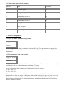
8 - 2D setup typical procedure (step by step)
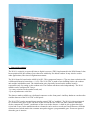
This is an example on how to operate N110 for 2D detector readout.
1) Detector/Discriminators preliminary check
Make sure you get correct fast NIM pulses from the anode (COM N110 input) and the cathodes (X1, X2,
Y1, Y2). N110 has internal 50 Ohms adapters. Check the serial number to know the edge sensitivity.
Minimum pulse width is 5 ns; usual pulse width is 10 to 20 ns. Minimum COMmon start (anode) to any
cathode is 3 ns. A 1 meter long cable does the job, otherwise a few events will be lost (rejected by the
pile-up detection logic).
2) N110 preliminary check
Red led FAIL NIM on: the mother board is dead (in general TDC FAIL will be a consequence).
Red led FAIL TDC on: the mezzanine board is dead.
Cycle power off/on. If it persists, N110 fails.
After power is just on, N110 enters a power saving sequence and is not operational yet. Both FAIL leds
must be off (as explained above) and PUP led must be on, and nothing else is happening. To wake up the
N110 TDC you must either press the front panel button or, by using the serial line, reset bit 3 in the
configuration register 2. So press the initialization button.
If the red led PUP remains on (all inputs being otherwise disconnected), the clock PLL does not lock.
Make sure you are selecting a correct clock reference (see next). Try internal medium speed clock (like
CFG3 = 2). If it persists, N110 fails. PUP led is normally off.
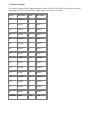
3) Set up the resolution
Select one out of the internal references. CFG3 (serial line address 3) even number. Odd number would
require an external reference.
4) Set up 2D operating mode
CFG1 (serial line address 1) = 0
5) Set the gate length
GATE (serial line address 0) = delay line length (in 25 ns units minus 50 ns offset, see 4.2).
Connect the anode to the COM input.
Observe the green led GATE. It is on when anode pulses are detected. Since this is proportional to the
actual event rate, this can be hardly seen below 10K events/s.
Monitor (oscilloscope) the GATE OUT signal (positive voltage), triggered by COM, duration as
programmed.
6) Disable the pile up rejection logic
For troubleshooting, expert users may skip that.
CFG2 (rotary switch) = 0.
CFG2 (serial line address 2) = 0x05 (beware serial differs from switch).
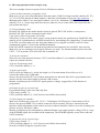
7) Check (again) the cathodes
Make sure (oscilloscope) you get X1, X2, Y1, Y2 during the GATE activity. Connect them to N110.
Observe the green led RDY. It is on when events have been recorded. This one is memorized (and
therefore mostly independent of the actual event rate) so that it should be visible even at low counting rate
(but not very low, like below 10Hz).
Monitor (oscilloscope) the (unfortunately) unlabeled bottom coax output (positive voltage). This is a copy
of the STROBE signal, also available on the output port. The STROBE typically occurs 200 ns after the
GATE terminates.
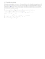
8) Activate the pile up rejection logic
CFG2 (rotary switch) = 3.
CFG2 (serial line address 2) = 0x35 (beware serial differs from switch).
Now the red led PUP flags the rejected events.