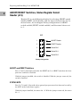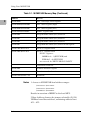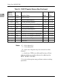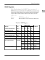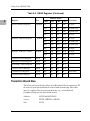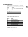
1
MVME334B
Multiprotocol
Communications
Controller Module
User’s Manual
VME334BA/UM1
Notice
While reasonable efforts have been m ad e to assu re the accu racy of this d ocu m ent,
Motorola, Inc. assu m es no liability resu lting from any om issions in this d ocu m ent,
or from the u se of the inform ation obtained therein. Motorola reserves the right to
revise this d ocu m ent and to m ake changes from tim e to tim e in the content hereof
w ithou t obligation of Motorola to notify any p erson of su ch revision or changes.
N o p art of this m aterial m ay be rep rod u ced or cop ied in any tangible m ed iu m , or
stored in a retrieval system , or transm itted in any form , or by any m eans, rad io,
electronic, m echanical, p hotocop ying, record ing or facsim ile, or otherw ise,
w ithou t the p rior w ritten p erm ission of Motorola, Inc.
It is p ossible that this p u blication m ay contain reference to, or inform ation abou t
Motorola p rod u cts (m achines and p rogram s), p rogram m ing, or services that are
not annou nced in you r cou ntry. Su ch references or inform ation m u st not be
constru ed to m ean that Motorola intend s to annou nce su ch Motorola p rod u cts,
p rogram m ing, or services in you r cou ntry.
Restricted Rights Legend
If the d ocu m entation contained herein is su p p lied , d irectly or ind irectly, to the U.S.
Governm ent, the follow ing notice shall ap p ly u nless otherw ise agreed to in
w riting by Motorola, Inc.
Use, d u p lication, or d isclosu re by the Governm ent is su bject to restrictions as set
forth in su bp aragrap h (c)(1)(ii) of the Rights in Technical Data and Com p u ter
Softw are clau se at DFARS 252.227-7013.
Motorola, Inc.
Com p u ter Grou p
2900 Sou th Diablo Way
Tem p e, Arizona 85282
Preface
The M V M E334B M ultiprotocol Communications M odule User’s M anual d escribes the
installation, com p onents, and configu rations of the MVME334B. The d ocu m ents
shou ld be u sed by anyone w ho w ants general as w ell as technical inform ation
abou t the MVME334B.
Related Documentation
The follow ing p u blications are ap p licable to the MVME334B and m ay p rovid e
ad d itional help fu l inform ation. If not ship p ed w ith this p rod u ct, they m ay be
p u rchased by contacting you r local Motorola sales office. N on-Motorola
d ocu m ents m ay be obtained from the sou rces listed .
Motorola
Publication N umber
D ocument Title
MVME334ABu g Debu gging Package User's Manu al
MVME709-1/ -2 Three Channel Transition Mod u le
Manu al
MVME334ABUG
User's
MVME709-1/ -2
MVME709-1/ -2 Three Channel Transition Mod u le Su p p ort
Inform ation
SIMVME709-1/ -2
MC68605 X.25 Protocol Controller (XPC) User’s Manu al
MC68605UM
MC68020 32-Bit Microp rocessor User's Manu al
MC68020UM
N OTE:
Althou gh not show n in the above list, each Motorola Com p u ter Grou p
m anu al p u blication nu m ber is su ffixed w ith characters w hich
rep resent the revision level of the d ocu m ent, su ch as / D2 or / UM1
(the second revision of a m anu al); a su p p lem ent bears the sam e
nu m ber as the m anu al bu t has a su ffix su ch as / A1 or / UM2A1 (the
first su p p lem ent to the m anu al).
The follow ing p u blications are available from the sou rces ind icated .
AN SI/ IEEE Std . 1014-1987 Versatile Backp lane Bu s: The Institu te of Electrical and
Electronics Engineers, Inc., 345 East 47th Street, N ew York, N Y 10017, USA.
(VMEbu s sp ecification)
SCN 68562 Du al Universal Serial Com m u nications Controller (DUSCC) Data
Sheet; Signetics Corp oration, 811 E. Arqu es Avenu e, P.O Box 3409, Su nnyvale, CA
94088-3409.
8254 Program m able Interval Tim er Data Sheet; Intel Corp oration, 3065 Bow ers
Avenu e, Santa Clara, CA 95051.
H D63450 DMA Controller Data Sheet; H itachi Am erica, Ltd ., Sem icond u ctor & IC
Division, 2000 Sierra Point Parkw ay, Brisbane, CA 94005-1819.
Manual Terminology
Throu ghou t this m anu al, a convention has been m aintained w hereby d ata and
ad d ress p aram eters are p reced ed by a character w hich sp ecifies the nu m eric
form at as follow s:
$
d ollar
sp ecifies a hexad ecim al
nu m ber
%
p ercent
sp ecifies a binary nu m ber
&
am p ersand
sp ecifies a d ecim al nu m ber
Unless otherw ise sp ecified , all ad d ress references are in hexad ecim al throu ghou t
this m anu al.
An asterisk (*) follow ing the signal nam e for signals w hich are level significant
d enotes that the signal is tru e or valid w hen the signal is low .
An asterisk (*) follow ing the signal nam e for signals w hich are edge significant
d enotes that the actions initiated by that signal occu r on high to low transition.
In this m anu al, assertion and negation are u sed to sp ecify forcing a signal to a
p articu lar state. In p articu lar, assertion and assert refer to a signal that is active or
tru e; negation and negate ind icate a signal that is inactive or false. These term s are
u sed ind ep end ently of the voltage level (high or low ) that they rep resent.
Safety Summary
Safety Depends On You
The follow ing general safety p recau tions m u st be observed d u ring all p hases of op eration, service, and
rep air of this equ ip m ent. Failu re to com p ly w ith these p recau tions or w ith sp ecific w arnings elsew here in
this m anu al violates safety stand ard s of d esign, m anu factu re, and intend ed u se of the equ ip m ent.
Motorola, Inc. assu m es no liability for the cu stom er's failu re to com p ly w ith these requ irem ents.
The safety p recau tions listed below rep resent w arnings of certain d angers of w hich Motorola is aw are.
You , as the u ser of the p rod u ct, shou ld follow these w arnings and all other safety p recau tions necessary
for the safe op eration of the equ ip m ent in you r op erating environm ent.
Ground the Instrument.
To m inim ize shock hazard , the equ ip m ent chassis and enclosu re m u st be connected to an electrical grou nd .
The equ ip m ent is su p p lied w ith a three-cond u ctor ac p ow er cable. The p ow er cable m u st either be p lu gged
into an ap p roved three-contact electrical ou tlet or u sed w ith a three-contact to tw o-contact ad ap ter, w ith
the grou nd ing w ire (green) firm ly connected to an electrical grou nd (safety grou nd ) at the p ow er ou tlet.
The p ow er jack and m ating p lu g of the p ow er cable m eet International Electrotechnical Com m ission (IEC)
safety stand ard s.
Do Not Operate in an Explosive Atmosphere.
Do not op erate the equ ip m ent in the p resence of flam m able gases or fu m es. Op eration of any electrical
equ ip m ent in su ch an environm ent constitu tes a d efinite safety hazard .
Keep Away From Live Circuits.
Op erating p ersonnel m u st not rem ove equ ip m ent covers. Only Factory Au thorized Service Personnel or
other qu alified m aintenance p ersonnel m ay rem ove equ ip m ent covers for internal su bassem bly or
com p onent rep lacem ent or any internal ad ju stm ent. Do not rep lace com p onents w ith p ow er cable
connected . Und er certain cond itions, d angerou s voltages m ay exist even w ith the p ow er cable rem oved .
To avoid inju ries, alw ays d isconnect p ow er and d ischarge circu its before tou ching them .
Do Not Service or Adjust Alone.
Do not attem p t internal service or ad ju stm ent u nless another p erson cap able of rend ering first aid and
resu scitation is p resent.
Use Caution When Exposing or Handling the CRT.
Breakage of the Cathod e-Ray Tu be (CRT) cau ses a high-velocity scattering of glass fragm ents (im p losion).
To p revent CRT im p losion, avoid rou gh hand ling or jarring of the equ ip m ent. H and ling of the CRT shou ld
be d one only by qu alified m aintenance p ersonnel u sing ap p roved safety m ask and gloves.
Do Not Substitute Parts or Modify Equipment.
Becau se of the d anger of introd u cing ad d itional hazard s, d o not install su bstitu te p arts or p erform any
u nau thorized m od ification of the equ ip m ent. Contact you r local Motorola rep resentative for service and
rep air to ensu re that safety featu res are m aintained .
Dangerous Procedure Warnings.
Warnings, su ch as the exam p le below , p reced e p otentially d angerou s p roced u res throu ghou t this m anu al.
Instru ctions contained in the w arnings m u st be follow ed . You shou ld also em p loy all other safety
p recau tions w hich you d eem necessary for the op eration of the equ ip m ent in you r op erating environm ent.
!
WARNING
Dangerou s voltages, cap able of cau sing d eath, are
p resent in this equ ip m ent. Use extrem e cau tion w hen
hand ling, testing, and ad ju sting.
!
WARNING
This equ ip m ent generates, u ses, and can rad iate electrom agnetic energy. It m ay cau se or be su scep tible to
electro-m agnetic interference (EMI) if not installed and
u sed in a cabinet w ith ad equ ate EMI p rotection.
Eu rop ean N otice: Board p rod u cts w ith the CE m arking com p ly w ith
the EMC Directive (89/ 336/ EEC). Com p liance w ith this d irective
im p lies conform ity to the follow ing Eu rop ean N orm s:
EN 55022 (CISPR 22)
Rad io Frequ ency Interference
EN 50082-1 (IEC801-2, IEC801-3, IEEC801-4)
Electrom agnetic Im m u nity
The p rod u ct also fu lfills EN 60950 (p rod u ct safety) w hich is essentially the requ irem ent for the Low Voltage Directive (73/ 23/ EEC).
This board p rod u ct w as tested in a rep resentative system to show com p liance w ith
the above m entioned requ irem ents. A p rop er installation in a CE-m arked system
w ill m aintain the requ ired EMC/ safety p erform ance.
Motorola ® and the Motorola sym bol are registered trad em arks of Motorola, Inc.
All other p rod u cts m entioned in this d ocu m ent are trad em arks or registered
trad em arks of their resp ective hold ers.
© Cop yright Motorola, Inc. 1995
All Rights Reserved
Printed in the United States of Am erica
Decem ber 1995
Contents
Chapter 1
General Information
Introd u ction .......................................................................................................... 1-1
Featu res.................................................................................................................. 1-1
Sp ecifications ........................................................................................................ 1-2
Cooling Requ irem ents ......................................................................................... 1-3
FCC Com p liance .................................................................................................. 1-4
General Descrip tion ............................................................................................. 1-4
Chapter 2
Preparing and Installing Your MVME334B
Introd u ction .......................................................................................................... 2-1
Unp acking You r H ard w are ................................................................................ 2-1
Configu ring You r MVME334B........................................................................... 2-1
VMEbu s Fu nctions Select H ead er (J5)........................................................ 2-4
Bu s Tim e-Ou t Select H ead er (J6)................................................................. 2-5
VMEbu s Requ ester Priority Level Select H ead er (J7) .............................. 2-6
Mod u le Ad d ress Mod e Select H ead er (J8) ................................................ 2-8
Mod u le Base Ad d ress Select H ead ers (J9, J14) ......................................... 2-9
ABORT/ RESET Sw itches, Statu s Register Select
H ead er (J12).................................................................................................. 2-10
ABORT and RESET Sw itches .............................................................. 2-10
STATUS BITS......................................................................................... 2-10
XPC Data Clock Select H ead er (J15) ......................................................... 2-11
Serial Port Configu ration Select (J18, J19)................................................ 2-13
DMAC Requ est Configu ration Select H ead er (J20)................................ 2-14
Rep lacing the OTP ROMs ................................................................................. 2-15
Rem oving a ROM Device ........................................................................... 2-15
Installing a ROM Device............................................................................. 2-15
Installing the MVME334B................................................................................. 2-16
Chapter 3
Using Your MVME334B
Introd u ction .......................................................................................................... 3-1
Controls and Ind icators ....................................................................................... 3-1
vii
RESET Sw itch ................................................................................................. 3-1
ABORT Sw itch ............................................................................................... 3-1
FAIL Ind icator................................................................................................ 3-2
Mem ory Map ........................................................................................................ 3-2
Register Descrip tions........................................................................................... 3-5
VMEbu s Com m and / Control Area ............................................................. 3-5
VMEbu s Statu s/ ID Location ....................................................................... 3-6
VMEbu s Interru p t Level Register ............................................................... 3-7
VMEbu s Interru p t Requ est Register........................................................... 3-7
Local Statu s Register ..................................................................................... 3-7
Bu s Tim e-Ou t Clear Location ...................................................................... 3-8
Watchd og Tim er Reset Location ................................................................. 3-9
Program m able Tim er .................................................................................... 3-9
XPC Registers............................................................................................... 3-11
DUSCC Registers......................................................................................... 3-12
DMAC Registers .......................................................................................... 3-15
Transition Board Bu s .................................................................................. 3-16
Ad d ress Mod ifier Register ......................................................................... 3-17
Softw are Consid erations ................................................................................... 3-19
H ard w are Initialization .............................................................................. 3-19
H ost/ MVME334B Dialog Initialization ................................................... 3-20
DUSCC Program m ing ................................................................................ 3-21
XPC Program m ing ...................................................................................... 3-23
VMEbu s Interru p ter Program m ing .......................................................... 3-23
VMEbu s Ad d ressing ................................................................................... 3-23
Reset Vector .................................................................................................. 3-24
Chapter 4
How the MVME334B Works
Introd u ction .......................................................................................................... 4-1
Overview ............................................................................................................... 4-1
VME System Interface ......................................................................................... 4-5
VMEbu s Slave Interface ............................................................................... 4-5
VME Com m and / Control Area ................................................................... 4-6
VMEbu s Master Interface............................................................................. 4-7
VMEbu s Requ ester ........................................................................................ 4-8
VMEbu s Interru p ter ...................................................................................... 4-9
Local Mem ory..................................................................................................... 4-10
RAM Mem ory .............................................................................................. 4-10
viii
ROM and EEPROM Mem ory..................................................................... 4-10
Tim ers .................................................................................................................. 4-11
Program m able Interval Tim er ................................................................... 4-11
Mu ltifu nction Cou nter/ Tim er ................................................................... 4-12
Watchd og Tim er .......................................................................................... 4-13
Bu s Tim er ...................................................................................................... 4-13
DTACK Generator ....................................................................................... 4-13
Local Statu s Register .......................................................................................... 4-14
Local Bu s Arbiter ................................................................................................ 4-14
Local Interru p ts .................................................................................................. 4-15
Bu s Errors ............................................................................................................ 4-18
Pow er-Up and Reset .......................................................................................... 4-19
SCN 68562 DUSCC Devices............................................................................... 4-19
Asynchronou s Op eration ........................................................................... 4-20
Synchronou s Op eration .............................................................................. 4-20
H D63450 DMAC ................................................................................................ 4-21
MC68605 XPC Devices ...................................................................................... 4-23
Perip heral Port Signals ...................................................................................... 4-24
MVME709-1/ -2 Three Channel Transition Mod u les .................................... 4-26
Index
ix
x
Figures
Figu re 2-1. MVME334B H ead er Locations ...................................................... 2-3
Figu re 4-1. MVME334B Block Diagram ........................................................... 4-2
xi
xii
Tables
Table 1-1. MVME334B Sp ecifications ................................................................ 1-2
Table 3-1. MVME334B Mem ory Map ................................................................ 3-3
Table 3-2. Program m able Tim er Registers ...................................................... 3-9
Table 3-3. Mod e 3 Bau d / Bit Rate Generation ............................................... 3-11
Table 3-4. XPC Directly Accessible Registers ................................................ 3-12
Table 3-5. DUSCC Register Mem ory Map ...................................................... 3-13
Table 3-6. DMAC Registers............................................................................... 3-15
Table 4-1. Local Interru p t Levels and Vectors ............................................... 4-16
Table 4-2. DUSCC/ DMAC Configu rations ......................................................... 4-22
xiii
xiv
1General Information
1
Introduction
This m anu al p rovid es general inform ation, p rep aration for u se and
installation instru ctions, op erating instru ctions, fu nctional
d escrip tion, and su p p ort inform ation for the MVME334B
Mu ltip rotocol Com m u nications Controller Mod u le.
Features
The featu res of the MVME334B inclu d e:
❏
MC68020 12.5 MH z m icrop rocessor
❏
4 MB RAM w ith p arity (d u al p orted )
❏
Fou r-channel Direct Mem ory Access Controller (DMAC)
❏
Fou r serial p orts w ith 50 to 38400 bau d in asynchronou s
m od e and
4 m egabits/ p er second in synchronou s m od e
❏
Tw o X.25 serial p orts w ith 4 m egabits/ p er second transfer
rate
❏
Tw o 4 MB One-Tim e-Program m able (OTP) ROMs containing
bootstrap and d ebu g firm w are
❏
2 KB u ser-p rogram m able EEPROM
❏
VMEbu s interru p ter
❏
VMEbu s slave interface (A32:D16/ 8 or A24:D16/ 8
com p atible)
❏
VMEbu s requ ester
❏
FAIL LED on front p anel
❏
RESET and ABORT sw itches on front p anel
1-1
1
General Inform ation
❏
Tim ers for p eriod ic interru p t generation, m alfu nction
m onitoring, bu s access su p ervision, and serial d ata clocking
Specifications
The MVME334B sp ecifications are given in Table 1-1. Cooling
requ irem ents and FCC com p liance are d iscu ssed in the sections
follow ing the table.
Table 1-1. MVME334B Specifications
Characteristics
Specifications
Pow er requ irem ents
+5 Vd c, 4.5 A m axim u m (4.0 A typ ical)
Microp rocessor
MC68020
Clock signal
12.5 MH z to MPU
Ad d ressing
Total ad d ress
range (on and offboard )
4 GB
OTP PROM
8 MB (tw o 4 MB 44 p in d evices, 256K x 32)
EEPROM
2 KB
Dynam ic RAM
4 MB
I/ O p orts
Tim ers
1-2
Six serial p orts
Total nu m ber
10
Watchd og
14-stage cou nter
Bu s
Monitors bu s requ ests and d ata transfer
cycles
Mu ltifu nction
Fou r 16-bit cou nter/ tim ers
(one for each serial channel)
Program m able
interval
One 16-bit tim e slice cou nter and
tw o Tx/ Rx d ata clock generators
DTACK
generator
One for inserting tw o w ait states
d u ring MPU local accesses
Cooling Requ irem ents
Table 1-1. MVME334B Specifications (Continued)
Characteristics
Specifications
Interru p t hand ler
Any or all onboard
Interru p t requ ester
Seven VMEbu s interru p ts
Bu s arbitration
Local bu s arbiter
Reset
RESET sw itch w hich can be enabled or
d isabled by softw are.
Op erating tem p eratu re
0° to 55° C at p oint of entry of forced air
(ap p roxim ately 150 LFM)
Storage tem p eratu re
-40° to 85° C
Relative hu m id ity
5% to 95% (noncond ensing)
Physical
characteristics
(exclu d ing front
p anel and
m ezzanine)
H eight
9.187 inches (233.35 m m )
Dep th
6.299 inches (160.0 m m )
Thickness
0.063 inches (1.6 m m )
Cooling Requirements
Motorola VMEm od u les are sp ecified , d esigned , and tested to
op erate reliably w ith an incom ing air tem p eratu re range from 0° C
to 55° C (32° F to 131° F) w ith forced air cooling.
Tem p eratu re qu alification is p erform ed in a stand ard Motorola
VMEsystem chassis. Tw enty-five w att load board s are inserted in
the tw o card slots, one on each sid e, ad jacent to the board u nd er test
to sim u late a high p ow er d ensity system configu ration. An
assem bly of three axial fans, rated at 71 CFM p er fan, is p laced
d irectly u nd er the MVME card cage. The incom ing air tem p eratu re
is m easu red betw een the fan assem bly and the card cage w here the
incom ing airstream first encou nters the m od u le u nd er test. Test
softw are is execu ted as the m od u le is su bjected to am bient
1-3
1
1
General Inform ation
tem p eratu re variations. Case tem p eratu res of critical, high p ow er
d ensity integrated circu its are m onitored to ensu re com p onent
vend ors sp ecifications are not exceed ed .
While the exact am ou nt of airflow requ ired for cooling d ep end s on
the am bient air tem p eratu re and the typ e, nu m ber, and location of
board s and other heat sou rces, ad equ ate cooling can u su ally be
achieved w ith 150 LFM flow ing over the m od u le. Less air flow is
requ ired to cool the m od u le in environm ents having low er
m axim u m am bients. Und er m ore favorable therm al cond itions it
m ay be p ossible to op erate the m od u le reliably at higher than 55° C
w ith increased air flow . It is im p ortant to note that there are several
factors, in ad d ition to the rated CFM of the air m over, w hich
d eterm ine the actu al volu m e of air flow ing over a m od u le.
FCC Compliance
This VMEm od u le (MVME334B) w as tested in an FCC-com p liant
chassis, and m eet the requ irem ents for Class A equ ip m ent. FCC
com p liance w as achieved u nd er the follow ing cond itions:
1. Shield ed cables on all external I/ O p orts.
2. Cable shield s connected to earth grou nd via m etal shell
connectors bond ed to a cond u ctive m od u le front p anel.
3. Cond u ctive chassis rails connected to earth grou nd . This
p rovid es the p ath for connecting shield s to earth grou nd .
4. Front p anels screw s p rop erly tightened .
For m inim u m RF em issions, it is essential that the cond itions above
be im p lem ented ; failu re to d o so cou ld com p rom ise the FCC
com p liance of the equ ip m ent containing the m od u les.
1-4
General Descrip tion
General Description
The MVME334B is a VMEm od u le base board and m ezzanine
com bination that p rovid es all the hard w are for a u niversal
intelligent controller for serial d ata com m u nications on six fu ll
d u p lex channels. Fou r of the channels are m u ltip rotocol channels
controlled by tw o SCN 68562 Du al Channel Universal
Com m u nication Controllers (DUSCC), located on the base board .
The other tw o channels are controlled by tw o MC68605 X.25
Protocol Controllers (XPC), located on the m ezzanine. A 4-channel
DMA Controller (DMAC) can be em p loyed for d ata transfers
betw een the DUSCC channels and local m em ory.
The m od u le has sockets containing u p to 8 MB of factory-su p p lied
OTP ROM and 2 KB of EEPROM on the base board , and a com p lete
32-bit m icrocom p u ter consisting of an MC68020 MPU and 4 MB of
RAM on the m ezzanine. This m icrocom p u ter controls the DUSCC
and XPC d evices and has access to the VMEbu s throu gh an
A32:D16/ 8 and A24:D16/ 8 m aster interface, either of w hich are
softw are selectable. The host system has access to the MVME334B
throu gh an A32:D16/ 8 and A24:D16/ 8 slave interface that can be
m ap p ed anyw here into the 4 GB VMEbu s ad d ress sp ace.
The host can send interru p t, reset, and com m and bytes to the
MVME334B and obtain statu s inform ation from the MVME334B
throu gh a VMEbu s com m and / control area in the d u al p orted local
RAM. VMEbu s accesses are su p p orted by bu s arbitration and
requ ester and interru p ter logic. Du al p ort logic enables the local
shared RAM to be accessed by either the local MPU or XPC d evices
or the DMA controller via the local bu s or by the host via the
VMEbu s.
The MVME334B can also op erate as a stand -alone u nit via a
m inim u m VMEbu s system controller.
Data can be transferred by the local MPU betw een local m em ory
and system m em ory, betw een local m em ory and DUSCC d evices,
betw een local m em ory and XPC d evices, and betw een local
1-5
1
1
General Inform ation
m em ory and DMAC/ DUSCC d evices. The fou r DUSCC channels
can be configu red for either half or fu ll d u p lex op eration, controlled
by the local MPU or DMAC.
Data transfer betw een local m em ory and the XPC d evices is carried
ou t u nd er DMA control u sing the DMA controller integrated into
each of the XPC d evices.
The MVME334B is d esigned for high p erform ance VMEbu s
system s, and becau se of its cap abilities of d ata link control, d ata
p re-/ p ost-p rocessing, and system m em ory access, can relieve the
host system of serial com m u nications tasks.
The MVME334B is intend ed for u se w ith the follow ing softw are
architectu re:
❏
The host establishes a stru ctu re in system m em ory or in the
MVME334B shared RAM for the transfer of high level
com m and s and m essages to and from the MVME334B.
❏
The MVME334B fetches com m and s from this stru ctu re,
execu tes the com m and s and retu rns statu s m essages.
❏
Both p olled and interru p t d riven m od es of op eration m ay be
u sed for the host/ MVME334B softw are interface.
Softw are d evelop m ent for the MVME334B is facilitated w ith the
MVME334ABu g d ebu g firm w are p ackage. This is a d ebu g/ m onitor
p rogram , contained in the OTP ROMs, that p rovid es a selfcontained p rogram m ing and op erating environm ent. The p rogram
interacts w ith the u ser throu gh p red efined com m and s that are
entered via a term inal. These com m and s allow you to: d isp lay and
m od ify m em ory or MVME334B registers, execu te a p rogram u nd er
variou s levels of control, and access inp u t/ ou tp u t resou rces.
Each of the six serial channels can be configu red to conform to
either the V.24 or V.35 stand ard s. This is im p lem ented on sep arate
board s:
❏
1-6
MVME709-1 Three Channel Transition Mod u le, w hich
su p p orts tw o X.25 channels and one m u ltip rotocol channel.
General Descrip tion
❏
MVME709-2 Three Channel Transition Mod u le, w hich
su p p orts three m u ltip rotocol channels.
The 8-bit p ort p ortion of the local d ata bu s (the transition board bu s)
is bu ffered and fed to connector P2 in ord er to p rovid e ad d itional
control and m onitor lines that m ay be requ ired for certain
exp ansions on the MVME709-1 and / or MVME709-2. The transition
m od u les are connected via ribbon cable to the A and C row s of the
MVME334B connector P2.
1-7
1
1
General Inform ation
1-8
2Preparing and Installing Your
MVME334B
2
Introduction
This chap ter p rovid es instru ctions for u np acking, p rep aring, and
installing the MVME334B m od u le.
Unpacking Your Hardware
Note
If the carton is d am aged u p on receip t, requ est that the
carrier's agent be p resent d u ring u np acking and
insp ecting of the equ ip m ent.
Unp ack the equ ip m ent from the ship p ing carton. Refer to the
p acking list and verify that all item s are p resent. Save the p acking
m aterial for storing and reship p ing of the m od u le.
Configuring Your MVME334B
To select the d esired configu ration and ensu re p rop er op eration of
the MVME334B m od u le, you m ay m ake certain changes to it before
installation. You m ake these changes by setting ju m p ers on head ers
on the board . The location of the head ers is illu strated in Figu re 2-1.
The m od u le has been factory tested and is ship p ed w ith factoryinstalled ju m p er configu rations that are show n in the follow ing
sections w ith the head er d escrip tions. The m od u le is op erational
w ith the factory-installed ju m p ers; the factory configu ration
p rovid es the system fu nctions requ ired for a VMEbu s system .
2-1
Prep aring and Installing You r MVME334B
You m ay w ish to m ake changes in the ju m p er arrangem ents for the
follow ing cond itions:
2
Function
VMEbu s fu nctions select
J5
Bu s tim e-ou t select
J6
VMEbu s requ ester p riority level select
J7
Mod u le ad d ress m od e select
J8
Mod u le base ad d ress select
J9, J14
ABORT/ RESET sw itches, statu s register select
J12
XPC d ata clock select
J15, J16
Serial p ort configu ration select (J18, J19)
J18, J19
DMAC requ est configu ration select
2-2
Header
J20
Configu ring You r MVME334B
2
J6
J5
2
1
J8
8
7
2
1
U12
8
7
3 1
4 2
J7
J9
S1
2
1
3 1
4 2
U19
S2
P1
FAIL
ABORT RESET
LED
24
23
1
9
J12
2
10
1
15
J14
2
16
Processor/Memory
Mezzanine
P2
J15
8
7
7
1
J16
8
1
2
2
4
2
4
2
6
2
J18
J19
J20
3
1
3
1
5
1
11387.00 9511
Figure 2-1. MVME334B Header Locations
2-3
Prep aring and Installing You r MVME334B
2
VMEbus Functions Select Header (J5)
H ead er J5 is p rovid ed for u se if the MVME334B is to be em p loyed
as the only bu s m aster. A single level arbiter, reset circu itry,
SYSRESET d river, and SYSFAIL m onitoring are im p lem ented and
can be enabled if the MVME334B is assigned to be the system
controller. The fu nctions are enabled if the p articu lar ju m p er is
installed . The as-ship p ed factory configu ration is w ith reset from
VMEbu s register enabled as show n below .
J5
VMEbus Arbiter
SYSRESET* Output
2-4
2
4
6
8
1
3
5
7
SYSFAIL* Output
Reset Input Register
Configu ring You r MVME334B
Bus Time-Out Select Header (J6)
2
H ead er J6 d eterm ines the tim e-ou t p eriod of the bu s tim er w hich
m onitors all bu s requ ests and d ata transfer cycles. The tim e-ou t
p eriod can be selected to be 57, 114, or 228 μs. A tim e-ou t p eriod of
infinity can also be selected , thu s effectively d isabling the bu s tim er.
The bu s tim e-ou t p eriod m u st be set to a valu e greater than the
longest tim e p eriod that m ay elap se betw een the assertion of a bu s
requ est and the recep tion of a bu s grant in the actu al system
configu ration.
The as-ship p ed factory configu ration is 114 μs as show n below :
J6
7
5
3
1
7
5
3
1
8
6
4
2
8
6
4
2
57 μs
114 μs
Factory Configuration
7
5
3
1
7
5
3
1
8
6
4
2
8
6
4
2
228 μs
No Time-Out
2-5
Prep aring and Installing You r MVME334B
2
VMEbus Requester Priority Level Select Header (J7)
H ead er J7 d eterm ines the VMEbu s requ ester p riority level. The
ju m p ers select the bu s requ est ou tp u t line and corresp ond ing bu s
grant d aisy chain. The as-ship p ed factory configu ration is level 3 as
show n below .
J7
2
4
6
8 10 12
14 16
18
1
3
5
7
13 15
17 19
9 11
20 22 24
21
23
Bus Request
Level 0
2
4
6
8 10 12
14 16
18
1
3
5
7
13 15
17 19
9 11
Bus Request
Level 1
2-6
20 22 24
21
23
Configu ring You r MVME334B
2
J7
2
4
6
8 10 12
14 16
18
1
3
5
7
13 15
17 19 21
9 11
20 22 24
23
Bus Request
Level 2
2
4
6
8 10 12
14 16
18
1
3
5
7
13 15
17 19 21
9 11
20 22 24
23
Bus Request
Level 3
Factory Configuration
2-7
Prep aring and Installing You r MVME334B
2
Module Address Mode Select Header (J8)
H ead er J8 d eterm ines w hether the m od u le is ad d ressed in stand ard
(A01 throu gh A23) or extend ed (A01 throu gh A31) m od e. If the
ju m p er is installed , the stand ard ad d ressing is u sed . If the ju m p er is
rem oved , extend ed ad d ressing is u sed . The as-ship p ed factory
configu ration, as show n below , is for extend ed ad d ressing m od e.
J8
3
1
3
1
4
2
4
2
Standard Addressing
Extended Addressing
Factory Configuration
2-8
Configu ring You r MVME334B
Module Base Address Select Headers (J9, J14)
2
H ead ers J9 and J14 d eterm ine the VMEbu s base ad d ress for the 4
MB onboard RAM (d u al p orted RAM at local ad d ress $FF800000$FFBFFFFF). Ad d ress lines A22 throu gh A31 corresp ond to these
head ers and allow base ad d ress to be m ap p ed in 4 MB increm ents
anyw here w ithin the 4 GB VMEbu s ad d ress sp ace.
Each ju m p er corresp ond s to a sp ecific ad d ress line as show n below .
Logic high levels on ad d ress lines m atch w ith rem oved ju m p ers
and logic low levels m atch w ith installed ju m p ers. The as-ship p ed
factory configu ration is w ith the A22, A23, and A25 ad d ress lines
set for logic low levels as show n below .
J9
3
4
J14
1
2
A22 A23
1
2
A31
3
4
A30
5
6
A29
7
8
A28
9
10
A27
11
12
A26
13
14
A25
15
16
A24
Axx = 0, if jumper is installed
Axx = 1, if jumper is removed
2-9
Prep aring and Installing You r MVME334B
2
ABORT/RESET Switches, Status Register Select
Header (J12)
H ead er J12 is a m u ltifu nction head er for selecting ABORT sw itch
d isable, RESET sw itch d isable, and the states of statu s bits 2-0. As
show n below , the as-ship p ed factory configu ration is ABORT
sw itch enabled , RESET sw itch enabled , and the statu s bits are set
to 1:
J12
1
2
ABORT Disable
3
4
RESET Disable
5
6
Status Bit 0
7
8
Status Bit 1
9
10
Status Bit 2
Factory Configuration
ABORT and RESET Switches
Pins 1-2 and 3-4 d eterm ine w hether the RESET and / or ABORT sw itch on the front
p anel are enabled or d isabled .
With the ju m p er installed , the sw itch is d isabled . With the ju m p er rem oved , the
sw itch is enabled .
STATUS BITS
Pins 5-6, 7-8, and 9-10 p rovid e three general p u rp ose statu s bits that can be read by
the MPU in the local statu s register.
With the ju m p er installed , the statu s bit = 0. With the ju m p er rem oved , the statu s
bit = 1.
2-10
Configu ring You r MVME334B
XPC Data Clock Select Header (J15)
2
H ead er J15 d eterm ines w hether the transm it and receive clocks for
the tw o X.25 Protocol Controller (XPC) d evices are taken from
connector P2 or from the onboard p rogram m able interval tim er.
The follow ing figu re and table show the ju m p er arrangem ents for
the XPC 0 and XPC 1 serial d ata clock selections. The as-ship p ed
factory configu ration is as show n below . N ote that J16 is not u sed
on the MVME334B.
J15
8
7
XPC 0 Rx
6
5
XPC 0 Tx
4
3
XPC 1 Rx
2
1
XPC 1 Tx
8
7
XPC 0 Rx
6
5
XPC 0 Tx
4
3
XPC 1 Rx
2
1
XPC 1 Tx
J16
XPC 0 and XPC1 Data Clock Selection
Factory Configuration
2-11
Prep aring and Installing You r MVME334B
2
D evice
Jumper
D ata Clock Selection
XPC 1
1-2 installed
Tx clock from p rogram m able interval tim er 2
(DCE configu ration - TRXC1 is ou tp u t)
XPC 1
1-2 rem oved
Tx clock from connector P2
(DTE configu ration - TRXC1 is inp u t)
XPC 1
3-4 installed
Rx clock from p rogram m able interval tim er 2
(DCE configu ration - RTXC1 is ou tp u t)
XPC 1
3-4 rem oved
Rx clock from connector P2
(DTE configu ration - RTXC1 is inp u t)
XPC 0
5-6 installed
Tx clock from p rogram m able interval tim er 1
(DCE configu ration - TRXC0 is ou tp u t)
XPC 0
5-6 rem oved
Tx clock from connector P2
(DTE configu ration - TRXC0 is inp u t)
XPC 0
7-8 installed
Rx clock from p rogram m able interval tim er 1
(DCE configu ration - RTXC0 is ou tp u t)
XPC 0
7-8 rem oved
Rx clock from connector P2
(DTE configu ration - RTXC0 is inp u t)
Note
Do not connect external clocks to connector P2 p ins
w hich are configu red as ou tp u ts by related ju m p er J15
connections.
The J15 ju m p er settings are also d ep end ent on the transition
m od u le connected to P2 (MVME709-1). For fu rther inform ation
refer to the transition m od u le u ser's m anu al.
2-12
Configu ring You r MVME334B
Serial Port Configuration Select (J18, J19)
2
H ead ers J18 and J19 allow you to select the d esired configu ration of
the serial p ort. N ote that the MVME334B ou tp u t is alw ays to P2;
there is no cu stom er op tion.
J18
J19
4
3
4
3
2
1
2
1
Factory Configuration
2-13
Prep aring and Installing You r MVME334B
2
DMAC Request Configuration Select Header (J20)
H ead er J20 is u sed to configu re the connections of Direct Mem ory
Access Controller (DMAC) channels 2 and 3. The DMAC su p p orts
either DUSCC0 fu ll d u p lex or DUSCC0 and DUSCC1 half d u p lex.
The follow ing figu re and table show the assignm ent of signals to
p ins on head er J20. The as-ship p ed factory configu ration is w ith
DUSCC0 fu ll d u p lex su p p ort.
J20
DUSCC0 TXDRQB
6
5
DUSCC0 TXDRQA
DMA Channel 3
4
3
DMA Channel 2
DUSCC1 RTXDRQB
2
1
DUSCC1 RTXDRQA
Factory Configuration
2-14
Jumper
D MAC Configuration
1-3 installed
DMAC channel 2 connected to DUSCC1
RTXDRQA
3-5 installed
DMAC channel 2 connected to DUSCC0 TXDRQA
2-4 installed
DMAC channel 3 connected to DUSCC1
RTXDRQB
4-6 installed
DMAC channel 3 connected to DUSCC0 TXDRQB
Rep lacing the OTP ROMs
Replacing the OTP ROMs
2
The MVME334B contains tw o sockets, labeled XU12 and XU19, that
hold tw o One-Tim e-Program m able (OTP) ROM d evices. These
ROMs contain bootstrap and d ebu g firm w are. If it becom es
necessary to rep lace these ROMs, follow the p roced u re below .
!
Caution
!
Caution
As su p p lied , the tw o sockets hold ROM d evices that contain
bootstrap firm w are. If these d evices are rem oved or corru p ted ,
you r system w ill not boot. Rep lacem ent ROM d evices m u st
p erform board initialization and boot cap ability.
The ROM com p onents are 44-p in integrated circu it
chip s; care shou ld be taken not to d am age the d evice
p ins.
Removing a ROM Device
1. Tu rn the p ow er off and d isconnect the p ow er cable from the
p ow er sou rce.
2. Using a PLCC extractor tool ap p rop riate to the 44-p in d evice,
carefu lly extract the ROM d evice from the socket.
3. Reconnect the p ow er cable to the p ow er sou rce and tu rn the
p ow er on.
Installing a ROM Device
1. Tu rn the p ow er off and d isconnect the p ow er cable from the
p ow er sou rce.
2. Carefu lly align p in 1 on the ROM d evice w ith p in 1 of the
socket.
With a firm action, p ress the ROM d evice d ow nw ard . The
Flash d evice shou ld d escend into the socket to be secu rely
installed .
3. Reconnect the p ow er cable to the p ow er sou rce and tu rn the
p ow er on.
Refer to the ROM and EEPROM M emory section in Chap ter 4 for
m ore d etails on the ROM m em ory and com p atible ROM d evices.
2-15
Prep aring and Installing You r MVME334B
2
Installing the MVME334B
After you have configu red the MVME334B’s head ers as need ed for
you r ap p lication, you can install it in the system as follow s:
1. Tu rn all equ ip m ent p ow er OFF and d isconnect the p ow er
cable from the AC p ow er sou rce.
!
Connecting m od u les w hile p ow er is ap p lied m ay resu lt
in d am age to com p onents on the m od u le.
Caution
!
Warning
Dangerou s voltages, cap able of cau sing d eath, are
p resent in this equ ip m ent. Use extrem e cau tion w hen
hand ling, testing, and ad ju sting.
2. Rem ove the chassis cover as instru cted in the equ ip m ent
u ser's m anu al.
3. Rem ove the filler p anel(s) from the ap p rop riate card slot(s) at
the front of the chassis. Do not install in card slot 1 u nless the
m od u le is configu red as system controller.
4. Insert the MVME334B into the selected card slot. Be su re the
m od u le is seated p rop erly into the connectors on the
backp lane. Fasten the m od u le in the chassis w ith the screw s
p rovid ed .
5. Install the ap p rop riate P2 p erip heral connector/ cable, w hich
is ship p ed w ith the transition m od u le, betw een the
MVME709-1 and / or MVME709-2 transceiver m od u les and
the connector on the backp lane corresp ond ing to the
MVME334B P2 connector. Be carefu l not to connect
incom p atible signals; e.g., VSB or VMX32) w ith P2.
6. At the MVME334B slot on the backp lane, rem ove the
IACKIN */ IACKOUT* ju m p er and the BGIN */ BGOUT*
ju m p er of the u sed p riority level. Install BGIN */ BGOUT*
ju m p ers on the u nu sed levels.
7. Carefu lly rep lace the cover you p reviou sly rem oved .
8. Tu rn the equ ip m ent p ow er ON .
2-16
3Using Your MVME334B
3
Introduction
This chap ter p rovid es inform ation on the MVME334B m em ory
m ap and variou s registers. Inclu d ed is an aid to softw are
d evelop m ent, ou tlining p oints that m u st be taken into
consid eration w hen d evelop ing softw are for the MVME334B.
Controls and Indicators
The MVME334B m od u le has a RESET sw itch, an ABORT sw itch,
and a FAIL LED ind icator, all of w hich are located on the front
p anel of the m od u le.
RESET Switch
The RESET sw itch triggers the reset circu it w hich generates a board
reset signal. The reset circu it cau ses a fu ll hard w are reset of the
MPU, the tw o XPC d evices, the tw o DUSCC d evices, the DMA
controller, and clears the VMEbu s interru p ter. The RESET sw itch
can be enabled / d isabled by ju m p er.
ABORT Switch
An ABORT sw itch is located on the front p anel. The ABORT sw itch
is norm ally u sed to abort p rogram execu tion and retu rn to the
d ebu gger.
Whenever the ABORT sw itch is p ressed w hile ru nning target cod e,
a “snap shot” of the p rocessor state is cap tu red and stored in the
target registers. When it is enabled , the ABORT cau ses a level 7
interru p t to the MC68020. The ABORT sw itch can be
enabled / d isabled by ju m p er.
3-1
Using You r MVME334B
FAIL Indicator
The red FAIL LED ind icator, located on the front p anel, ind icates a
severe, nonrecoverable m alfu nction of the MVME334B. The FAIL
LED is lit w hen w atchd og tim e-ou t occu rs. Also, a ju m p er op tion
asserts SYSFAIL on the VMEbu s.
3
Memory Map
The MVME334B local ad d ress area extend s from $FF800000 to
$FFFFFFFF and is show n in Table 3-1.
The local RAM base ad d ress is $FF800000 and extend s for 4 MB to
$FFBFFFFF. The second byte contains the VMEbu s interru p t
statu s/ ID.
The local RAM is shared betw een the local bu s m asters and the
VMEbu s via a d u al p ort controller. The local ad d ress area of
$FF800000 to $FFBFFFFF m ay therefore be accessed from the
VMEbu s at the ad d ress area Base Ad d ress +($000000-$3FFFFF).
Base Ad d ress d enotes the ju m p er selectable (J9, J14, and J8) m od u le
VMEbu s base ad d ress, and can be m ap p ed anyw here into the 4 GB
VMEbu s ad d ress sp ace in 4 MB increm ents.
The local ROM base ad d ress is $FFF80000 and extend s to 8 MB.
All local d evices and registers, inclu d ing the EEPROM, are resid ent
in the 128 KB area above local ROM, starting at local ad d ress
$FFFE0000.
3-2
Mem ory Map
Table 3-1. MVME334B Memory Map
3
Address
D evice
$00000000-$FF7FFFFF
VMEbu s
$FF800000
Local RAM
$FF800001
Local RAM (VMEbu s interru p t vector location)
$FF800000-$FFBFFFEF
Du al p orted RAM (general read / w rite area) This area
is accessible to the host from VMEbu s at Base Ad d ress
+ ($000000-$3FFFEF) (See N ote 2)
$FFFEE000-$FFFEE0FF
Reserved (access cau ses BERR*)
$FFBFFFF0-$FFBFFFFF
Du al p orted RAM (com m and / control area) This area
is accessible to the host from VMEbu s at Base Ad d ress
+ ($3FFFF0-$3FFFFF) (See N ote 2)
$FFF80000-$FFFBFFFF
ROM. Only 256K 32-bit w id e w ord s are ad d ressable
from the CPU. On the board , A18 is hard w ired to 0
and A19 is hard w ired to 1.
$FFFE0000
Local statu s register
$FFFE4000
VMEbu s interru p t level register
$FFFE4010
VMEbu s interru p t requ est register
$FFFE8000
Watchd og tim er reset
$FFFEC000
XPC 0 reserved
$FFFEC001
XPC 0 com m and register/ sem ap hore register
$FFFEC002
XPC 0 reserved
$FFFEC003
XPC 0 interru p t vector register
$FFFEC004-$FFFEC005
XPC 0 d ata register (high)
$FFFEC006-$FFFEC007
XPC 0 d ata register (low )
$FFFED000
XPC 1 reserved
$FFFED001
XPC 1 com m and register/ sem ap hore register
$FFFED002
XPC 1 reserved
3-3
Using You r MVME334B
Table 3-1. MVME334B Memory Map (Continued)
3
Address
D evice
$FFFED003
XPC 1 interru p t vector register
$FFFED004-$FFFED005
XPC 1 d ata register (high)
$FFFED006-$FFFED007
XPC 1 d ata register (low )
$FFFEF000-$FFFEF0FF
DMAC register table
$FFFF0000
Program m able tim er (PIT) cou nter 0
$FFFF0001
Program m able tim er (PIT) cou nter 1
$FFFF0002
Program m able tim er (PIT) cou nter 2
$FFFF0003
Program m able tim er (PIT) control w ord register
$FFFF1000-$FFFF103F
DUSCC 0 register table
$FFFF2000-$FFFF203F
DUSCC 1 register table
DUSCC registers:
OMRB bit 6 = 1 ($FFFF202B) and
PCRB bit 2 = 0 ($FFFF202E)
are reserved for WRITE WRON G PARITY
Transition board bu s
$FFFF4000
Ad d ress m od ifier register
$FFFF8000
Bu s tim e-ou t clear location
$FFFFC000-$FFFFC7FF
EEPROM
Notes 1. Access to MVME334B local ad d ress ranges:
$FFC00000-$FFF7FFFF
$FFFC0000-$FFFDFFFF
$FFFEE000-$FFFEEFFF
Resu lts in assertion of BERR* to the local MPU.
2. Base Ad d ress d enotes the ju m p er selectable (J9, J14)
VMEbu s board base ad d ress, containing ad d ress lines
A31 - A22.
3-4
Register Descrip tions
Register Descriptions
The MVME334B contains a nu m ber of registers and m em ory
locations for controlling variou s onboard fu nctions and for
inform ation interchange w ith the VME host system .
3
The follow ing sections contain d etails of all local registers in the
ord er that they occu r in the m em ory m ap . The d escrip tions inclu d e:
❏
A short d escrip tion of the register fu nction.
❏
The location of the register in the MVME334B ad d ress m ap .
❏
The typ e of access (BYTE, WORD, or LWORD; READ or
WRITE).
❏
The size of the register (BYTE, WORD, or LWORD).
VMEbus Command/Control Area
A local reset/ interru p t register and a local com m and / statu s
register are m ap p ed into the u p p erm ost 16 bytes of the d u al p orted
local RAM. A w rite from the VMEbu s to even locations w ith the
valu e $01xx send s an au tovector 1 interru p t to the MVME334B, and
a w rite from the VMEbu s to even locations w ith the valu e $02xx
resets the MVME334B. Od d locations can be read or w ritten by
either the VMEbu s or the local MPU and allow m essage bytes to be
p assed , even locations are w rite only. Any w rite from the local
MPU to the reset/ interru p t register neither resets nor interru p ts the
local MPU.
Ad d ress lines:
A31-A22, A21-A1
Ad d ress:
VMEbu s base ad d ress + $3FFFF0-3FFFFF
VMEbu s access:
WORD: WRITE $01xx to even locations for
MVME334B au tovector 1 interru p t
WORD: WRITE $02xx to even locations for
MVME334B reset
(w here xx can be u sed for p assing a m essage byte)
3-5
Using You r MVME334B
BYTE: READ
(od d locations contain statu s byte from MVME334B)
MVME334B access: BYTE: WRITE to od d locations
(statu s byte to VMEbu s)
3
BYTE: READ from od d locations
(com m and byte from VMEbu s)
Size:
WORD
Local
Address
Reset/Interrupt
Register
Command/Status
Byte
VMEbus
Address
$FFBFFFF0
N ot u sed RES IN T
User d efined
BA +$3FFFF0
$FFBFFFF2
N ot u sed RES IN T
User d efined
BA +$3FFFF2
$FFBFFFF4
N ot u sed RES IN T
User d efined
BA +$3FFFF4
$FFBFFFF6
N ot u sed RES IN T
User d efined
BA +$3FFFF6
$FFBFFFF8
N ot u sed RES IN T
User d efined
BA +$3FFFF8
$FFBFFFFA
N ot u sed RES IN T
User d efined
BA +$3FFFFA
$FFBFFFFC
N ot u sed RES IN T
User d efined
BA +$3FFFFC
$FFBFFFFE
N ot u sed RES IN T
User d efined
BA +$3FFFFE
Bits:
15-10
7-0
Note
9
8
BA (Base Ad d ress) refers to ad d ress lines A31 - A22.
VMEbus Status/ID Location
The p rogram m able VMEbu s statu s/ ID is w ritten into the second
location of the local RAM. This byte is sent to the local MPU w hen
an interru p t acknow led ge is received at a level equ al to the content
of the interru p t level register, thu s selecting the d esired vector from
the host vector table for the interru p t service rou tine.
3-6
Register Descrip tions
Ad d ress:
$FF800001
Access:
BYTE, WRITE (statu s/ ID)/ READ
Size:
BYTE
3
VMEbus Interrupt Level Register
An interru p t level of 1 to 7 m u st be w ritten into the VMEbu s
interru p t level register by the local MPU before a VMEbu s interru p t
is generated .
Ad d ress:
$FFFE4000
Access:
BYTE, WRITE only (level 1-7)
Size:
BYTE
VMEbus Interrupt Request Register
When the MVME334B need s to generate a VMEbu s interru p t, the
local MPU accesses the VMEbu s interru p t requ est register. It m u st
be ensu red that the statu s/ ID location ($FFE00001) and the
interru p t level register ($FFFE4000) are set before a VMEbu s
interru p t is generated .
Ad d ress:
$FFFE4010
Access:
BYTE, WORD or LWORD; READ or WRITE
Size:
BYTE
Local Status Register
The local statu s register is a 6-bit read only register that reflects the
statu s of 3 system signals and 3 ju m p er p ositions.
Ad d ress:
$FFFE0000
Access:
BYTE or WORD; READ only
Size:
BYTE
3-7
Using You r MVME334B
3
Bit
D escription
5
SYSFAIL
This bit reflects the statu s of the VMEbu s
line SYSFAIL*.
4
VMEbu s Interru p t
Acknow led ge
When set, this bit ind icates that the
MVME334B interru p t requ est to the
VMEbu s has been acknow led ged . When
reset, the bit ind icates that an MVME334B
interru p t requ est to the VMEbu s is
p end ing.
3
VMEbu s Tim e-ou t
(STOUT
When set, this bit ind icates that either a
VMEbu s requ est has not been granted in
tim e or that the VMEbu s access has not
been acknow led ged by DTACK. This bit is
reset if the bu s tim e-ou t clear location is
accessed .
2-0
Read able Ju m p er
Positions
These bits reflect the settings of p ins 5-10
on head er J12.
Bus Time-Out Clear Location
Any access by the local MPU to the bu s tim e-ou t clear location
resets the bu s tim e-ou t bit 6 (STOUT) of the local statu s register. The
STOUT bit is set if the bu s tim er tim es ou t d u ring any bu s access of
the local MPU or the XPCs.
3-8
Ad d ress:
$FFFF8000
Access:
BYTE, WORD or LWORD; WRITE or READ
Size:
BYTE
Register Descrip tions
Watchdog Timer Reset Location
The w atchd og tim er m u st be regu larly reset by the MPU w ithin 168
m s p eriod s in ord er to p revent it from tim ing ou t and generating a
failu re signal. The w atchd og tim er is reset by sim p ly accessing the
w atchd og tim er reset location w ith any read or w rite op eration.
Ad d ress:
$FFFE8000
Access:
BYTE or WORD; READ or WRITE
Size:
BYTE
Programmable Timer
The 8254 Program m able Interval Tim er (PIT) contains three
sep arate 16-bit tim ers. Tim er 0 is u sed for generating tim e slice
p eriod s of u p to 1.342 second s and tim ers 1 and 2 are d ed icated as
bau d rate generators for XPC 0 and XPC 1. The follow ing table
show s the p rogram m able tim er registers.
Table 3-2. Programmable Timer Registers
Address
Register
Size
Access
$FFFF0000
Cou nter/ statu s 0 register
BYTE
READ/ WRITE
$FFFF0001
Cou nter/ statu s 1 register
BYTE
READ/ WRITE
$FFFF0002
Cou nter/ statu s 2 register
BYTE
READ/ WRITE
$FFFF0003
Control w ord register
BYTE
WRITE
For p eriod ic tim e slice generation, it is recom m end ed that the
squ are w ave op eration m od e (m od e 3) be u sed for tim er 0. In this
m od e, after load ing the ap p rop riate control w ord and initializing
the cou nt register to the d esired valu e, the cou nt d ow n is started by
transferring the contents of the cou nt register to the cou nting
elem ent. The cou nting elem ent is then d ecrem ented by tw o on each
3-9
3
Using You r MVME334B
su cceed ing clock p u lse. When the cou nt reaches zero, the cou nter
ou tp u t line is toggled and the cou nt register contents are reload ed
into the cou nting elem ent and the p rocess rep eats ind efinitely.
3
The tim e slice cou nter p eriod for m od e 3 is given by the form u la:
Tim e slice p eriod = (preloaded value + 1) * 20.48 m icrosecond s
Preload valu e range: m inim u m = 2, m axim u m = 0 (corresp ond ing
to $10000)
Do not load $0001 into the cou nter, becau se in squ are w ave m od e it
w ou ld generate a constant TTL low ou tp u t level instead of a
p eriod ic squ are w ave.
For non-p eriod ic, softw are synchronized tim e slice generation, it is
recom m end ed that the interru p t on term inal cou nt op eration m od e
(m od e 0) be u sed for tim er 0. In this m od e, the cou nter ou tp u t line
goes low u p on load ing the cou nt byte and the cou nting elem ent is
d ecrem ented by 1 on each su cceed ing clock p u lse. Up on reaching
zero, the cou nter ou tp u t line goes high u ntil the cou nt registers are
reload ed .
The tim e slice cou nter p eriod for m od e 0 is given by the form u la:
Tim e slice p eriod = (preloaded value + 1) * 20.48) m icrosecond s
The rising ed ge of the cou nter 0 ou tp u t signal is latched and
generates an au tovectored level 2 interru p t requ est to the local
MPU. The latched interru p t requ est is reset w hen acknow led ged by
the MPU.
If tim ers 1 and 2 are to be u sed as bau d rate generators, squ are w ave
m od e (m od e 3) is recom m end ed . The table below show s cou nter
p reload valu es for m od e 3 generation of typ ical bau d and bit rates.
3-10
Register Descrip tions
Table 3-3. Mode 3 Baud/Bit Rate Generation
Counter Value
Baud Rate
(Bits/second)
Hexadecimal
D ecimal
2
2
3072000
4
4
1536000
8
8
0768000
.
.
.
.
.
.
$A0
160
38400
$140
320
19200
$280
640
9600
$500
1280
4800
$A00
2560
2400
$1400
5120
1200
$2800
10240
600
$5000
20480
300
3
XPC Registers
The X.25 Protocol Controller (XPC) d evices contain a large nu m ber
of registers, only fou r of w hich are d irectly accessible by the MPU.
These registers are m ap p ed into the MVME334B m em ory m ap as
show n below . XPC0 and XPC1 corresp ond to serial p orts 0 and 1,
resp ectively, on the MVME709-1 m od u le.
Detailed inform ation as to the accessibility and p rogram m ing of the
com p lete XPC register set can be fou nd in the M 68605 X.25 Protocol
Controller (XPC) User’s M anual.
3-11
Using You r MVME334B
Table 3-4. XPC Directly Accessible Registers
3
D evice
Address
Register
Size
Access
XPC 0
$FFFEC001
Com m and
BYTE
WRITE
XPC 0
$FFFEC001
Sem ap hore
BYTE
READ
XPC 0
$FFFEC003
Interru p t Vector
BYTE
READ/ WRITE
XPC 0
$FFFEC004
Data (high)
WORD
WRITE
XPC 0
$FFFEC006
Data (low )
WORD
WRITE
XPC 1
$FFFED001
Com m and
BYTE
WRITE
XPC 1
$FFFED001
Sem ap hore
BYTE
READ
XPC 1
$FFFED003
Interru p t Vector
BYTE
READ/ WRITE
XPC 1
$FFFED004
Data (high)
WORD
WRITE
XPC 1
$FFFED006
Data (low )
WORD
WRITE
DUSCC Registers
The Du al Universal Serial Com m u nications Controller (DUSCC)
d evices contain a large nu m ber of registers, all of w hich can be
d irectly ad d ressed . For accesses to sp ecific registers in these
d evices, the register ad d resses are taken as offsets to the resp ective
base ad d ress. The DUSCC register ad d ress m ap is show n in Table
3-5. The DUSCC Data Book contains d etailed inform ation abou t the
u se of these registers.
Base ad d ress:
DUSCC 0 $FFFF1000
DUSCC 1 $FFFF2000
Tw o locations in DUSCC 1 are reserved to control the fu nction
w rite w rong p arity (refer to the RAM M emory section in Chap ter 4).
These locations are bit 2 in OMR(B) and bit 6 in PCR(B). After reset,
these bits are cleared and are therefore in the norm al op eration
3-12
Register Descrip tions
m od e. Bit 2 of OMR(B) m u st be set to 1 to activate the w rite w rong
p arity fu nction. It m u st also be ensu red that bit 6 of PCR(B) is set
to 0.
DUSCC 1 channel A corresp ond s to serial p ort 4 on the MVME7091. DUSCC 0 channel A, DUSCC 0 channel B and DUSCC 1 channel
B corresp ond to serial p orts 2, 3, and 5 on the MVME709-2.
Table 3-5. DUSCC Register Memory Map
Address
Bits (1)
654321
Abbrev.
Register N ame
Mode
Affected
by
Reset
C00000
CMR1
Channel Mod e Register 1
R/ W
Yes - 00
C00001
CMR2
Channel Mod e Register 2
R/ W
Yes - 00
C00010
S1R
SYN 1/ Sec Ad d ress 1 Register
R/ W
No
C00011
S2R
SYN 2/ Sec Ad d ress 2 Register
R/ W
No
C00100
TPR
Transm itter Param eter Register
R/ W
Yes - 00
C00101
TTR
Transm itter Tim ing Register
R/ W
No
C00110
RPR
Receiver Param eter Register
R/ W
Yes - 00
C00111
RTR
Receiver Tim ing Register
R/ W
No
C01000
CTPRH
Cou nter/ Tim er Preset Register H igh
R/ W
No
C01001
CTPRL
Cou nter/ Tim er Preset Register Low
R/ W
No
C01010
CTCR
Cou nter/ Tim er Control Register
R/ W
No
C01011
OMR
Ou tp u t and Miscellaneou s Register
R/ W
Yes - 00
C01100
CTH
Cou nter/ Tim er H igh
R
No
C01101
CTL
Cou nter/ Tim er Low
R
No
C01110
PCR
Pin Configu ration Register
R/ W
Yes - 00
C01111
CCR
Channel Com m and Register
R/ W
No
C100xx
TxFIFO
Transm itter FIFO
W
No
3-13
3
Using You r MVME334B
Table 3-5. DUSCC Register Memory Map (Continued)
3
Address
Bits (1)
654321
Abbrev.
Register N ame
Mode
Affected
by
Reset
C101xx
RxFIFO
Receiver FIFO
R
No
C11000
RSR
Receiver Statu s Register
R/ W(2)
Yes - 00
C11001
TRSR
Tx and Rx Statu s Register
R/ W(2)
Yes - 00
C11010
ICTSR
Inp u t+Cou nter/ Tim er Statu s Register
R/ W(2)
Yes
D11011
GSR1
General Statu s Register
R/ W(2)
Yes - 00
C11100
IER
Interru p t Enable Register
R/ W
Yes - 00
C11101
N ot Used
011110
IVR
Interru p t Vector Register Unm od ified
R/ W
Yes - 0F
111110
IVRM
Interru p t Vector Register Mod ified
R
Yes - 0F
011111
ICR
Interru p t Control Register
R/ W
Yes - 00
111111
N ot Used
Notes 1. C = 0 for channel A.
C = 1 for channel B.
D = d on't care. Register m ay be accessed as either
channel.
x = d on't care. FIFOs are ad d ressable at any of fou r
ad jacent ad d resses to allow them to be ad d ressed as
BYTE/ WORD/ LWORD.
2. A w rite to this register m ay p erform a statu s resetting
op eration.
3-14
Register Descrip tions
DMAC Registers
Each of the fou r channels in the DMAC has a sep arate set of
registers. Detailed d escrip tions of these registers can be fou nd in the
H D63450 d ocu m entation (refer to the Related Documentation section
in the Preface of this m anu al). The follow ing table lists the DMAC
register ad d ress offsets from the DMAC base ad d ress, and the
register sizes.
Ad d ress:
$FFFEE000 (base ad d ress)
Access:
READ/ WRITE (excep t CER w hich is READ only)
Table 3-6. DMAC Registers
Address Offset
Register
Size
General Control Register
Comment
CH0
CH1
CH2
CH3
BYTE
$FF
$FF
$FF
$FF
Base Fu nction Cod es
BYTE
$39
$79
$B9
$F9
Device Fu nction Cod es
BYTE
$31
$71
$B1
$F1
Channel Priority Register
BYTE
$2D
$6D
$AD
$ED
Mem ory Fu nction Cod es
BYTE
$29
$69
$A9
$E9
Error Interru p t Vector
BYTE
$27
$67
$A7
$E7
N orm al Interru p t Vector
BYTE
$25
$65
$A5
$E5
Base Ad d ress Register
LWORD
$1F
$5F
$9F
$DF
lo byte
$1E
$5E
$9E
$DE
lo-m id byte
$1D
$5D
$9D
$DD
hi-m id byte
$1C
$5C
$9C
$DC
hi byte
$1B
$5B
$9B
$DB
lo byte
$1A
$5A
$9A
$DA
hi byte
Base Transfer Cou nter
WORD
3-15
3
Using You r MVME334B
Table 3-6. DMAC Registers (Continued)
Address Offset
3
Register
Size
Device Ad d ress Register
LWORD
Mem ory Ad d ress Register
Mem ory Transfer Cou nter
CH1
CH2
CH3
$17
$57
$97
$D7
lo byte
$16
$56
$96
$D6
lo-m id byte
$15
$55
$95
$D5
hi-m id byte
$14
$54
$94
$D4
hi byte
$0F
$4F
$8F
$CF
lo byte
$0E
$4E
$8E
$CE
lo-m id byte
$0D
$4D
$8D
$CD
hi-m id byte
$0C
$4C
$8C
$CC
hi byte
$0B
$4B
$8B
$CB
lo byte
$0A
$4A
$8A
$CA
hi byte
LWORD
WORD
Comment
CH0
Channel Control Register
BYTE
$07
$47
$87
$C7
Sequ ence Control Register
BYTE
$06
$46
$86
$C6
Op eration Control Register
BYTE
$05
$45
$85
$C5
Device Control Register
BYTE
$04
$44
$84
$C4
Channel Error Register
BYTE
$01
$41
$81
$C1
Channel Statu s Register
BYTE
$00
$40
$80
$C0
read only
Transition Board Bus
The 8-bit p ortion of the local bu s is bu ffered and fed to connector P2
in ord er to p rovid e ad d itional control and m onitoring lines that
m ay be requ ired for certain exp ansions; e.g., an ad d itional
p erip heral chip on the transition board .
3-16
Ad d ress:
$FFFF3000-$FFFF3003
Access:
BYTE; WRITE or READ
Size:
BYTE
Register Descrip tions
Address Modifier Register
The ad d ress m od ifier register contains the 6-bit cod e u sed for
VMEbu s accesses via the MVME334B VMEbu s m aster interface.
Ad d ress:
$FFFF4000
Access:
BYTE; WRITE only (ad d ress m od ifier cod e)
Size:
BYTE
Bit
D escription
7-6
N ot u sed
5-0
VMEbu s ad d ress m od ifier cod e
Extended Addressing Address Modifier Codes:
AM Code
Function
$09
N on-p rivileged d ata access
$0A
N on-p rivileged p rogram access
$0B
N on-p rivileged block transfer
$0D
Su p ervisory d ata access
$0E
Su p ervisory p rogram access
$0F
Su p ervisory block transfer
User-Defined Address Modifier Codes:
AM Code
Function
$10-$1F
N on-p rivileged d ata access
3-17
3
Using You r MVME334B
Short Addressing Address Modifier Codes:
3
AM Code
Function
$29
Su p ervisory Access
$2D
N on-p rivileged access
Standard Addressing Address Modifier Codes:
3-18
AM Code
Function
$39
N on-p rivileged d ata access
$3A
N on-p rivileged p rogram access
$3B
N on-p rivileged block transfer
$3D
Su p ervisory d ata access
$3E
Su p ervisory p rogram access
$3F
Su p ervisory block transfer
Softw are Consid erations
Software Considerations
When d evelop ing softw are for the MVME334B, there are a nu m ber
of p oints that m u st be taken into accou nt. Som e of these are
hard w are d ep end ent and others are d ep end ent u p on the d riving
softw are or the intend ed ap p lication. The follow ing sections ou tline
these p oints and give recom m end ations w here necessary. It is
intend ed as a general gu id e and shou ld be treated as su ch.
Hardware Initialization
After a board reset has been carried ou t, the p arity bits in RAM are
in an u nd efined state and m u st be initialized .
When RAM has been initialized , shad ow registers shou ld be set u p
in RAM for any of the w rite only registers in the MVME334B that
w ill be altered d u ring op eration. Follow ing this, the w rite only
registers them selves can be initialized .
The MVME334B contains the follow ing w rite only registers that
cannot be read by the local MPU:
❏
VME interru p t level register
❏
Ad d ress m od ifier register
The w atchd og and tim e slice cou nters are both in an u nd efined
state after a board reset is carried ou t. The w atchd og tim er has a
p eriod of 168 m s and m u st be reset w ithin this p eriod (by an access
to $FFFE8000) to p revent it from tim ing ou t and generating a
system fail signal. The tim e slice cou nter (cou nter 0 of the
p rogram m able tim er/ cou nter 8254) m u st be load ed w ith a start
cou nt valu e if p eriod ic interru p ts are requ ired .
If cou nters 1 and 2 of the p rogram m able tim er/ cou nter 8254 are to
be u sed for clocking the XPC d ata transfers, these m u st be
initialized to p rovid e the correct clock rate.
The DUSCC d evices m u st be initialized to bring them into a d efined
state, d ep end ent u p on d riving softw are and ap p lication.
3-19
3
Using You r MVME334B
The MPU m u st establish the station table, transm it fram e
sp ecification table, and receive fram e sp ecification table for u se by
each of the XPC d evices. The tw o XPC d evices can then be
initialized and the ad d resses of their resp ective station table p assed
to them by the MPU.
3
Note
The XPC d evices d o not com e ou t of softw are or
hard w are reset w ithou t the transm it clock ap p lied .
Host/MVME334B Dialog Initialization
The MVME334B is intend ed for u se w ith the follow ing softw are
architectu re:
❏
The host establishes a stru ctu re in system m em ory or in the
MVME334B shared m em ory for the transfer of high level
com m and s and m essages to and from the MVME334B.
❏
The MVME334B fetches com m and s from this stru ctu re,
execu tes the com m and s, and retu rns statu s m essages.
❏
Both p olled and interru p t d riven m od es of op eration m ay be
u sed for the host/ MVME334B softw are interface. With
interru p t d riven d ialog, the VMEbu s interru p t register m u st
be load ed w ith the interru p t level and statu s/ ID assigned to
the MVME334B. If they are not to be changed d u ring
op eration, the interru p t level and statu s/ ID can be
p rogram m ed into ROM; otherw ise, they m u st be p assed to
the MVME334B by the host.
The VME com m and / control area in the u p p erm ost 16 bytes of the
d u al p orted p ortion of local RAM is p rim arily intend ed for u se
d u ring system initialization, althou gh it can also be u sed d u ring
norm al op eration. The host can send bytes of inform ation as w ell as
a local reset or interru p t to the MVME334B and the MVME334B can
retu rn statu s inform ation to the host via the VME com m and /
control area.
3-20
Softw are Consid erations
Inform ation p assed from host to MVME334B throu gh the VME
com m and / control area m ay inclu d e:
❏
Interru p t level and statu s/ ID assigned to the MVME334B
❏
Pointers to stru ctu res set u p in system m em ory or in the
MVME334B shared m em ory
❏
Ad d ress m od ifier cod es
Inform ation p assed from MVME334B to host throu gh the VME
com m and / control area m ay inclu d e:
❏
Pow er u p self-test statu s
❏
Initialization statu s
❏
Malfu nction and error cod es
DUSCC Programming
The p rogram m ing of the DUSCC d evices is d ep end ent u p on
d riving softw are and intend ed ap p lication.
In ord er to ease the start-u p p roced u re, a basic rou tine for
initialization of DUSCC 0 for asynchronou s term inal I/ O is show n
below . This rou tine w aits for character inp u t on transition board
channel 2 or 3 (both configu red as DCE) and echoes back any
received character.
3-21
3
Using You r MVME334B
BEGIN
;
SETUP
3
MOVE.B #$0F,$FFFF3001
MOVE.B
#07,CMR1A
MOVE.B
#07,CMR1B
MOVE.B
#$38,CMR2A
MOVE.B
#$38,CMR2B
MOVE.B
#$7F,TPRA
;set DTR2*, DTR3*, DTR4*, DTR5*
;no parity, async mode
;normal mode, polled/int
;1 stop bit,RTS, CTS, 8-bit
Tx char
MOVE.B
MOVE.B
#$7F,TPRB
#13,RPRA
MOVE.B
MOVE.B
MOVE.B
MOVE.B
MOVE.B
MOVE.B
MOVE.B
MOVE.B
MOVE.B
MOVE.B
MOVE.B
MOVE.B
MOVE.B
MOVE.B
MOVE.B
MOVE.B
MOVE.B
#13,RPRB
#$2D,RTRA
#$2D,RTRB
#1,OMRA
#1,OMRB
#$A6, PCRA
#$A6, PCRB
#$3D, TTRA
#$3D, TTRB
#0,CCRA
#0,CCRB
#$40,CCRA
#$40,CCRB
#02,CCRA
#02,CCRB
#$42,CCRA
#$42,CCRB
;control RTS, no DCD, 8-bit
Rx char
;
;
Read and
;
DUSCC0RA; BTST.B
BEQ
MOVE.B
DUSCC0RB; BTSTB.B
BEQ
MOVE.B
BRA
;
END SETUP
3-22
;Rx = BRG clk, 9600 baud
;set RTS2*
;set RTS3*
;IDC pin 45; RTS Txclk x 1
;IDC pin 9; RTS Txclk x 1
;Tx = BRG clock 9600 baud
;reset Tx
;reset Rx
;enable Tx
;enable Rx
echo input character
#0, GSR
;check for RxA ready
DUSCC0RB
;check DUSCC0B
RX_FIFOA, TX_FIFOA;echo character
#4, GSR
;check for RxB ready
DUSCC0RA
;check DUSCC0A
RX_FIFOB, TX_FIFOB;echo character
DUSCC0RA
Softw are Consid erations
XPC Programming
Initialization of the XPC d evices consists of the MPU p assing the
station table ad d ress and fu nction cod e, system configu ration
inform ation, and the XPC interru p t vector to each of the XPC
d evices. Fu rther p rogram m ing of the XPC d evices is d ep end ent
u p on d riving softw are and intend ed ap p lications.
VMEbus Interrupter Programming
Execu te the follow ing p roced u re step by step in ord er to generate a
VMEbu s interru p t requ est from the MVME334B to the host system :
1. Check the local statu s register for SIRQ acknow led ged .
2. Store the d esired statu s/ ID in the statu s/ ID location.
3. Store the d esired interru p t level in the interru p t level register.
4. Generate the VMEbu s interru p t by read ing or w riting to the
interru p t requ est register.
VMEbus interrupt acknowledged? ($FFFE0000) = (bit 4 (SIRQ) = 1)
LOOPUNTIL SIRQ ACKNOWLEDGED
.
.
($FFFE0001) : = Status/ID
.
.
($FFFE4000) : = Interrupt level
.
.
Generate VMEbus interrupt by reading or writing memory location
$FFFE4010
VMEbus Addressing
Data transfers to and from system m em ory are carried ou t by the
local MPU d irectly ad d ressing the area from $00000000 to
$FF7FFFFF via the VMEbu s m aster interface. This is su p p orted by
p rogram m able ad d ress m od ifier cod es.
3-23
3
Using You r MVME334B
Reset Vector
After a board reset, for the first tw o m em ory cycles, onboard ROM
is m ap p ed locally into the ad d ress sp ace starting at $00000000 and
the MPU fetches the reset vector from the bottom ad d resses of local
ROM. Therefore, the firm w are resid ent in local ROM m u st p rovid e
the initial su p ervisor stack p ointer valu e at $FFF80000-$FFF80003
and p rogram cou nter valu e at $FFF80004-$FFF80007.
3
3-24
4How the MVME334B Works
4
Introduction
This chap ter p rovid es the fu nctional d escrip tion of the MVME334B
at block level. The fu nctional d escrip tion p rovid es an overview of
the m od u le, follow ed by a d etailed d escrip tion of each section of the
m od u le.
Overview
The MVME334B is a VMEm od u le for d riving serial transceiver
d evices either as a stand -alone board or as a versatile interface
betw een the VMEbu s and the transceivers. It is show n in fu nctional
block form in Figu re 4-1.
The MVME334B contains a com p lete m icrocom p u ter bu ilt arou nd
an MC68020 m icrop rocessor w hich relieves the system host
p rocessor from serial com m u nications controlling tasks. Data
p rep rocessing and p ostp rocessing, insertion and d eletion of control
inform ation, error control, and flow control are typ ical tasks that
the MVME334B p rocessor can carry ou t.
The local m em ory consists of 4 MB of d ynam ic RAM w ith byte
p arity generation and checking, 2 KB of EEPROM, and 8 MB of
factory- or u ser-su p p lied ROM.
The 4 MB of local RAM is 32/ 16 bits w id e and is accessible by the
MPU, DMAC, and XPC d evices. Read accesses are carried ou t w ith
zero w ait states, w ith one w ait state being inserted for w rite
accesses. The local RAM is controlled by a d u al p ort controller and
can also be accessed by a host system via the VMEbu s. Accesses
from the VMEbu s are 16 bits w id e.
4-1
4-2
Figure 4-1. MVME334B Block Diagram
ABORT RESET
ABORT/RESET
CIRCUIT
WATCHDOG
TIMER
FAIL
LOCAL
INTERRUPT
HANDLER
LOCAL
ADDRESS
DECODER
MASTER/SLAVE
INTERFACE
LOCAL BUS
ARBITER
COMMNICATION
REGISTER SET
2 KB
EEPROM
CONTROL
AND STATUS
REGISTERS
SYSTEM CONTR.
REQUESTER
INTERRUPTER
TIMERS
X.25
CONTROLLERS
8 MB
ROM
DMA
CONTROLLER
SERIAL
COMMUNICATION
CONTROLLERS
4 MB
DRAM
11388.00 9511
DRAM
DUAL PORT
CONTROLLER
PERIPHERAL
BUS
TRANSCEIVER
VMEBS AND I/O CONNECTOR P2
4
MC68020
MICROPROCESSOR
VMEBUS
ACCESS
CONTROL
VMEBUS CONNECTOR P1
H ow the MVME334B Works
Overview
The MVME334B is ship p ed w ith tw o 4 MB OTP ROMs installed in
EPROM sockets on the base board , su p p lying 8 MB of read -only
m em ory. These ROMs contain bootstrap firm w are and the d ebu g
m onitor. Refer to Chap ter 2 for cau tions to observe w hen rep lacing
these d evices. ROM read s are 32 bits w id e.
A 2 KB EEPROM is p rovid ed for non-volatile storage of p aram eters
that m ay requ ire m od ification. Accesses to the EEPROM are byte
w id e.
Tw o SCN 68562 DUSCC, tw o MC68605 XPC d evices, and a
H D63450 DMAC are controlled by the MPU. Each DUSCC is a d u al
channel, m u ltip rotocol, serial d ata inp u t/ ou tp u t d evice cap able of
op erating asynchronou sly at u p to 38400 bau d or synchronou sly at
u p to 4 m egabits p er second . Bau d rates, d ata characteristics, and
control fu nctions are softw are selectable. Each XPC is a serial d ata
inp u t/ ou tp u t d evice that fu lly im p lem ents the X.25
recom m end ation LAPB p roced u re and can op erate safely at u p to
10 m egabits p er second if clocked externally.
The DMAC can be u sed to control either tw o DUSCC channels fu ll
d u p lex or fou r DUSCC channels half d u p lex.
The local m icrop rocessor accesses VME system m em ory throu gh an
op tion A32:D16/ 8 or A24:D16/ 8 VMEbu s m aster interface w ith
p rogram m able ad d ress m od ifier cod es. The bu s arbitration is
p erform ed by a Release-When-Done (RWD) bu s requ ester that
op erates in the “early release of BBSY*” m od e and w ith a selectable
p riority level. The hand shake control logic contains a bu s tim er
w hich, after a ju m p er selectable tim e p eriod , term inates an
u nsu ccessfu l attem p t to transfer d ata over the VMEbu s.
Interru p ts to the VME system host p rocessor are generated by a
VMEbu s interru p ter w ith p rogram m able p riority level and
statu s/ ID.
The u p p erm ost 16 bytes of the d u al p orted local RAM are u sed for
resetting and interru p ting the MVME334B and for single-byte
transm ission/ recep tion of control/ statu s bytes betw een the host
and the MVME334B. The VME system host p rocessor can access the
d u al p orted local RAM throu gh an A32:D16/ 8 or A24:D16/ 8 slave
4-3
4
H ow the MVME334B Works
interface w hose ad d ress m od ifier d ecod er is p rogram m ed to allow
stand ard and extend ed d ata accesses. The d u al p orted RAM can be
m ap p ed anyw here in the 4 GB VMEbu s ad d ress sp ace in 4 MB
increm ents and u sed for d ata interchange w ith the host.
The MVME334B also contains ten p rogram m able tim er/ cou nters:
4
❏
One 16-bit tim e slice cou nter that generates p eriod ical
interru p ts to the MPU. The p eriod is p rogram m able betw een
40.96 μs and 1.342 second s for tim e sliced softw are concep ts.
❏
Tw o Tx/ Rx d ata clock generators for the XPC d evices,
allow ing bit rates of u p to 3.072 m egabits p er second .
❏
Fou r 16-bit general p u rp ose tim ers (tw o in each DUSCC
d evice) for u se as bit rate generators, event cou nters, etc.
❏
One w atchd og tim er w ith a tim e-ou t p eriod of 168 m s that
m u st be p eriod ically reset by the local MPU before this cou nt
is reached . If the w atchd og tim er tim es ou t, the FAIL LED on
the front p anel is tu rned on and a ju m p er selectable op tion
also asserts the SYSFAIL* line on the VMEbu s.
❏
One bu s tim er that m onitors all VME and local bu s
transactions and , if an acknow led ge signal is not received
w ithin the p reset tim e, generates a BERR* signal and sets a bit
in the local statu s register. The tim er p eriod m ay be ju m p er
selected to be either 57, 114, or 228 μs or infinity.
❏
One DTACK* generator for inserting tw o w ait states d u ring
MPU local accesses to ROM, EEPROM, and onboard
registers.
These tim ers are d escribed in greater d etail in the Timers
section in this chap ter.
All p erip heral signals, at TTL level, are available at connector
P2 on the MVME334B. From there they can be fed throu gh a
flat ribbon cable to the MVME709-1 or MVME709-2. Three
Channel Transition Mod u le. These m od u les configu re the
signals to conform to the V.24 or V.35 stand ard s for the serial
channels and p rovid e 25-p in su b-D connectors on the front
p anel for the connection of p erip heral d evices.
4-4
VME System Interface
VME System Interface
The follow ing sections d escribe the VME system op erations
su p p orted by the MVME334B. This inclu d es the slave interface,
com m and / control area, m aster interface, requ ester and ,
interru p ter.
The VMEbu s interface p rovid es the signal p ath betw een the
MVME334B and the VMEbu s backp lane. The interface com p lies
w ith all requ irem ents for the signal d river/ receiver characteristics
and bu s op eration p rotocols, as sp ecified in the VMEbu s
sp ecification.
VMEbus Slave Interface
The MVME334B VMEbu s slave interface is of the A32:D16/ 8 and
A24:D16/ 8 typ e and allow s access from the VMEbu s to the local
RAM m em ory. The p ortion of the local RAM area ($FF800000$FFBFFFFF) is shared betw een the local bu s m asters (MPU and XPC
d evices) and the VMEbu s via a d u al p ort controller and m ay be
accessed from VMEbu s ad d resses Base Ad d ress + ($000000$3FFFFF). The Base Ad d ress is ju m p er selectable (head ers J9 and
J14) on ad d ress lines A22-A31 in 4 MB increm ents and can be
m ap p ed anyw here in the 4 GB VMEbu s ad d ress sp ace as show n
below .
Base Address + ($000000-$3FFFEF)
Du al p orted RAM - general
read / w rite (4 MB m inu s 16 bytes)
Base Address + ($3FFFF0-$3FFFFF)
Du al p orted RAM com m and / control area (16 bytes)
The local RAM area at VMEbu s Base Ad d ress + ($000000-$3FFFEF)
is d irectly accessible for d ata interchange betw een the VMEbu s and
the MVME334B. The average access tim e throu gh the slave
interface to the shared RAM is ap p roxim ately 600 ns for read and
w rite accesses.
4-5
4
H ow the MVME334B Works
The 16-byte local RAM area at VMEbu s Base Ad d ress + ($3FFFF0$3FFFFF) is em p loyed as a com m and / control area and is d escribed
in the V M Ebus Command/Control Area section in Chap ter 3.
The ad d ressing cap ability of the VMEbu s slave interface is
d eterm ined by the configu ration of head er J8 w hich allow s
stand ard (A24) or extend ed (A32) ad d ressing. The interface refers
to the ap p rop riate ad d ress lines for d ecod ing, d ep end ent on the
ad d ress m od ifier cod e.
4
The slave interface is restricted to d ata access only. Therefore, the
host cannot execu te p rogram cod e in the d u al p orted RAM. The
slave interface d ata bu s is 16 bits w id e (D16) and the host MPU
m u st therefore be configu red to access the d u al p orted RAM w ith
either w ord or byte accesses. The d u al p orted local RAM is accessed
from the VMEbu s throu gh the slave interface w ith ad d ress m od ifier
cod es $3D and $39 for stand ard su p ervisory and stand ard nonp rivileged d ata access; $0D and $09 for extend ed su p ervisory and
extend ed non-p rivileged d ata access.
VME Command/Control Area
The MVME334B contains a 16-byte area at the u p p er end of the d u al
p orted p ortion of local RAM that can be u sed for the transfer of
control and statu s inform ation betw een the VME system host
p rocessor and the MVME334B.
A w rite access from the VMEbu s to even locations in the
com m and / control area Base Ad d ress + ($3FFFFx) w ith the valu e
$x1xx resu lts in an interru p t being generated in the MVME334B. A
w rite access from the VMEbu s to even locations w ith the valu e
$x2xx resu lts in the MVME334B being reset. Accesses from the
VMEbu s to od d locations in the com m and / control area m ay be
read or w rite, allow ing the exchange of com m and and statu s
inform ation betw een the host and the MVME334B. It is therefore
p ossible w ith a single w ord access w ith the valu e $x1xx to generate
an interru p t in the MVME334B and also p ass a control byte to the
MVME334B.
4-6
VME System Interface
There is no w ay to check d irectly w hether the MVME334B has
recognized an interru p t p laced in the com m and / control area.
Therefore, to avoid loss of interru p ts, you shou ld d esign you r
softw are so that the MVME334B inform s the host, throu gh a
“read y” m essage anyw here in the shared RAM, that its interru p t
has been p rocessed .
4
VMEbus Master Interface
The MVME334B contains a VMEbu s m aster interface betw een the
local MPU and the VMEbu s. The ad d ressing cap abilities of this
interface are softw are p rogram m able via the ad d ress m od ifier
d ecod er register. Short (A16), stand ard (A24), or extend ed (A32)
ad d ressing is im p lied by the u se of the ap p rop riate ad d ress
m od ifier cod e. The MVME334B VMEbu s d ata w id th is 16 bit (D16).
The fu ll VMEbu s ad d ress band w id th from $00000000 to $FF7FFFFF
m ay be accessed , the rem aining area from $FF800000 to $FFFFFFFF
being occu p ied by local d evices, registers, and RAM.
A m inim u m VMEbu s system controller is im p lem ented on the
MVME334B, allow ing the m od u le to op erate as the sole bu s m aster
in a m inim u m configu ration VME system . The fu nctions
im p lem ented are p ow er u p reset circu itry, SYSRESET d river,
SYSFAIL m onitoring, and a single level arbiter. These fu nctions are
selectable via ju m p ers and are to be enabled if the MVME334B is
assigned to be the system controller.
The m aster interface is not restricted to d ata transfer accesses, bu t it
is recom m end ed that p rogram cod e not be execu ted from the
VMEbu s. The cod e shou ld be d ow nload ed into local m em ory and
execu ted from there.
The ad d ress m od ifier register is a 6-bit w rite only register and is
u sed to p ass ad d itional ad d ress inform ation to the VMEbu s. This
inform ation can be u sed in a nu m ber of d ifferent w ays, d ep end ent
u p on the configu ration of the system (this is exp lained in m ore
d etail in the VMEbu s sp ecification. Details of the sep arate bits and
location of the ad d ress m od ifier register can be fou nd in the Address
4-7
H ow the MVME334B Works
M odifier Register section in Chap ter 3. It m u st be ensu red that the
ap p lication softw are correctly sets the ad d ress m od ifier register
p rior to any VMEbu s op erations.
Program m ing consid erations w ith resp ect to VMEbu s ad d ressing
are given in the V M Ebus Addressing section in Chap ter 3.
4
VMEbus Requester
System m em ory accesses are controlled in the MVME334B by the
VMEbu s requ ester w hich op erates in the “early release of BBSY*”
m od e. In this m od e BBSY* is negated as soon as the MVME334B has
asserted its ad d ress strobe signal. The VMEbu s requ ester has a
ju m p er selectable (J9) p riority level of from 0 to 3. Refer to the
V M Ebus Requester Priority Level Select Header section in Chap ter 2 for
d etails.
When the ad d ress d ecod er logic d etects that the MPU has asserted
an ad d ress that is off-board , the VMEbu s requ ester asserts a bu s
requ est at the selected p riority level. When a bu s grant is received
at that level, the bu s requ ester asserts the bu s bu sy signal and
enables the VMEbu s m aster interface.
If the VMEbu s requ ester d etects a bu s grant signal for w hich it has
no requ est p end ing, the VMEbu s requ ester asserts its bu s grant ou t
signal for d ow nstream d aisy chain p articip ants.
VMEbu s requ ests are m onitored by tim e-ou t circu itry that
generates BERR* and sets a bit in the MVME334B local statu s
register if bu s grant or DTACK* is not received w ithin the selected
tim e p eriod . The tim e-ou t p eriod is selectable via head er J6 as
d escribed in the Bus Time-out Select Header section in Chap ter 2.
If the VMEbu s requ est from the MPU coincid es w ith an attem p t to
access MVME334B local RAM by the cu rrent bu s m aster, a d u al
p ort lockou t cond ition occu rs. To alleviate this p roblem , the bu s
requ ester forces a retry to the local MPU u p on occu rrence of a
lockou t. If the bu s requ est by the local MPU contains a read -m od ifyw rite cycle, the MPU d oes not accep t a retry and the bu s requ ester
asserts BERR* to the local MPU.
4-8
VME System Interface
VMEbus Interrupter
Interru p t requ ests from the MVME334B to the host system are
generated by a VMEbu s interru p ter w ith p rogram m able interru p t
level and statu s/ ID. The local MPU m u st w rite the level into the
interru p t level register ($FFFE4000) and the statu s/ ID into the
statu s/ ID location ($FF800001) before any interru p t requ ests are
initiated .
When the local MPU accesses the VMEbu s interru p t requ est
register at ad d ress $FFFE4010 w ith any read or w rite instru ction,
the VMEbu s interru p t requ est signal is asserted at the selected level.
When the interru p t acknow led ge at that level is received , the
VMEbu s interru p ter issu es a statu s/ ID requ est to the d u al p ort
controller w hich fetches the VMEbu s statu s/ ID from local RAM
and asserts it to VMEbu s lines D00-D07. The interru p ter logic locks
ou t an MPU access to the interru p t level register u ntil after the
p end ing requ est is acknow led ged .
If the VMEbu s interru p ter d etects an interru p t acknow led ge signal
for w hich it has no interru p t p end ing, the VMEbu s interru p ter
asserts its IACKOUT signal for d ow nstream d aisy chain
p articip ants.
The local statu s register contains a bit that reflects the actu al state of
the interru p t requ est ou tp u t. The local MPU can p oll this bit to
d eterm ine w hether the interru p t has been acknow led ged by the
host. After acknow led gm ent, the bit is au tom atically cleared by the
interru p ter.
The V M Ebus Status/ID Location section contains d etails of the
VMEbu s statu s/ ID location. Details of the VMEbu s interru p t
requ est register are given in the V M Ebus Interrupt Request Register
section. The V M Ebus Interrupt Level Register section contains d etails
of the VMEbu s interru p t level register. These three sections are in
Chap ter 3.
4-9
4
H ow the MVME334B Works
Local Memory
The MVME334B contains 4 MB of d ynam ic RAM w ith byte p arity,
tw o ROM sockets for 8 MB of ROM, and a 2 KB EEPROM. Accesses
to the local RAM are controlled by a d u al p ort controller, allow ing
d irect access by the local MPU or XPC d evices or access via the slave
interface throu gh the VMEbu s.
4
RAM Memory
The MVME334B RAM m em ory array consists of one 4 MB d evice.
Local MPU read accesses are carried ou t w ith zero w ait states and
one w ait state is inserted for MPU w rite accesses. Accesses by the
XPC d evices are carried ou t w ith one w ait state. The local RAM base
ad d ress is m ap p ed to $FF800000 in the local m em ory m ap .
The RAM is organized 32 bits w id e and allow s byte, w ord , or
longw ord accesses by any d evice, as w ell as u naligned transfers by
the local MPU.
Byte p arity generation and checking d u ring RAM accesses are
carried ou t au tom atically, w ith p arity errors generating an
au tovectored level 7 interru p t to the MPU. VMEbu s and XPC access
p arity errors assert the BERR* line. A “w rite w rong p arity” fu nction
is available for p arity logic test p u rp oses. A general p u rp ose ou tp u t
p ort of DUSCC 2 is u sed to assert this fu nction (refer to the DUSCC
Registers section in Chap ter 3).
The d ynam ic RAM is refreshed au tom atically by refresh logic, this
being ind ep end ent of RAM accesses or any other board activity. A
refresh cycle, u sing CAS before RAS refresh m od e and the refresh
cou nters in the RAM d evices, is carried ou t every 10 μs.
ROM and EEPROM Memory
Tw o 44-p in ROM sockets are p rovid ed on the MVME334B for local
firm w are. The sockets contain tw o factory-installed 4 MB, 256K x 32
OTP ROMs, w hich are p rogram m ed w ith bootstrap firm w are and
4-10
Tim ers
the MVME334ABu g d ebu g firm w are. Refer to Chap ter 2 for
cau tions that ap p ly w hen rep lacing these ROMs w ith u ser-su p p lied
ROMs.
The ROM area is m ap p ed into one contigu ou s block starting at
ad d ress $FFF80000. This is organized as longw ord w id e m em ory
w ith only aligned accesses being allow ed .
After reset, the ROMs are m ap p ed to starting location 0 d u ring the
first tw o accesses by the MPU to fetch the stack p ointer and
p rogram cou nter.
A 2K x 8 bit EEPROM d evice is p rovid ed to enable system
p aram eters to be stored w hen p ow er is rem oved from the m od u le.
Its base ad d ress is m ap p ed to $FFFFC000 in the local m em ory m ap .
After a w rite access to this d evice, w hich m u st be bytew ise, fu rther
accesses to the d evice are not allow ed for 10 m s.
A DTACK generator is p rovid ed and allow s installation of ROM,
PROM, or EPROM d evices w ith m axim u m 300 ns access tim es.
Timers
The MVME334B contains a nu m ber of tim er/ cou nters for p eriod ic
interru p t generation, MVME334B m alfu nction m onitoring, bu s
access su p ervision, and serial d ata clocking.
Programmable Interval Timer
The 8254 Program m able Interval Tim er (PIT) on the MVME334B
contains three sep arate p rogram m able 16-bit tim ers.
Tim er 0 is d ed icated as a p rogram m able tim e slice cou nter for tim e
p eriod s of u p to 1.342 second s. This tim e slice cou nter can be u sed
to generate p eriod ic interru p ts to the MPU for tim e sliced softw are
concep ts. The cou nter contains a 16-bit p reload register and
continu ou sly cou nts d ow n from the load ed valu e to 0 at w hich
p oint it generates an au tovectored level 2 interru p t requ est to the
MPU. The interru p t requ ests are latched and reset w hen
4-11
4
H ow the MVME334B Works
acknow led ged by the MPU. The tim e slice cou nter is clocked from
the 12.5 MH z MPU clock d ivid ed by 256, resu lting in a clock
frequ ency of 48.828 KH z. This gives a p rogram m able tim e slice
p eriod of betw een 40.96 μs (if the cou nter is load ed w ith $0002 (refer
to note below ), and 1.342 second s (if it is load ed w ith $0000
(corresp ond ing to $10000), w ith p rogram m able increm ents of 20.48
μs.
4
!
Caution
Do not load $0001 into the cou nter becau se in squ are w ave m od e
that w ou ld generate a constant TTL low ou tp u t instead of a p eriod ic
squ are w ave.
If the p reload valu e is changed w hile the tim e slice cou nter is
ru nning, the cu rrent p eriod is not affected , and the new valu e is
u sed w ith the next p eriod .
Refer to the Programmable Timer section in Chap ter 3 for tim e slice
p eriod calcu lation.
Tim ers 1 and 2 are d ed icated as Tx/ Rx d ata clock generators for
XPC d evices 0 and 1, resp ectively. Both tim ers are clocked w ith
6.144 MH z allow ing a m axim u m bit rate of 3.072 m egabits p er
second .
Multifunction Counter/Timer
Each of the tw o DUSCC d evices contains tw o 16-bit
cou nter/ tim ers, one for each serial channel. These cou nter/ tim ers
can be p rogram m ed to fu nction as bit rate generators, event
cou nters, interval tim ers, and m ay also be u sed for bit length
m easu rem ents or to cou nt transm itted or received characters.
The SCN 68562 DUSCC d ata book contains d etailed inform ation
abou t the p rogram m ing and u se of these cou nter/ tim ers.
4-12
Tim ers
Watchdog Timer
The w atchd og tim er is a free ru nning cou nter that generates a
system fail signal u p on tim ing ou t to ind icate a severe,
nonrecoverable m alfu nction of the MVME334B. Up on tim ing ou t, it
lights the FAIL LED on the front p anel and a ju m p er op tion (J5) for
the w atchd og tim er also asserts the SYSFAIL* line on the VMEbu s.
The w atchd og tim er is a 14 stage cou nter w hich is clocked at a
frequ ency of 48.828 KH z, resu lting in a fu ll cou nt tim e after reset of
168 m illisecond s. In ord er to p revent the cou nter tim ing ou t and
generating the above signals, it m u st be regu larly reset by the
MVME334B softw are before it tim es ou t. This is achieved by sim p ly
ad d ressing the w atchd og tim er reset location ($FFFE8000). N o d ata
transfer is necessary.
Bus Timer
The bu s tim er m onitors all bu s requ ests and d ata transfer cycles and
if the ad d ressed d evice d oes not resp ond w ith a d ata transfer
acknow led ge signal w ithin the p reset tim e, it generates a BERR*
signal and sets a bit in the local statu s register. A tim e-ou t p eriod of
either 57, 114, or 228 μs, or infinity m ay be selected by head er J6.
The tim e-ou t p eriod m u st be set to a valu e greater than the longest
tim e p eriod that m ay elap se betw een the assertion of a bu s requ est
and the recep tion of a bu s grant in the actu al system configu ration.
DTACK Generator
The DTACK generator is a w ait state generator for MPU accesses to
ROM and all onboard registers. Tw o w ait states are inserted in
ord er to accom m od ate ROM/ EEPROM d evices w ith 300 ns access
tim es.
4-13
4
H ow the MVME334B Works
Local Status Register
The MVME334B contains a local statu s register (at local ad d ress
$FFFE0000) that enables the local MPU to m onitor variou s
MVME334B fu nctions. The local statu s register is a 6-bit read only
register w ith the follow ing fu nctions:
4
Bit
D escription
5
Reflects the statu s of the VMEbu s SYSFAIL* line.
4
VMEbu s interru p t acknow led ge bit (SIRQ) and ind icates
that the interru p t requ est to the VMEbu s has been
acknow led ged .
3
Tim e-ou t statu s bit (STOUT) and is set if an ad d ressed
d evice d oes nor resp ond before the tim e-ou t sp ecified by
head er J6.
2-0
Connected d irectly to head er J12 and reflect w hether the
corresp ond ing ju m p er is installed or rem oved . They are
intend ed for general p u rp ose u se and cou ld , for exam p le,
be u sed to encod e sp ecific tart u p cond itions.
Local Bus Arbiter
The local MPU is the p erm anent m aster of the local bu s u ntil one of
the p otential bu s m asters issu es a bu s requ est. When either an XPC
d evice, the DMA controller, or the d u al p ort controller requ ests
local bu s m astership , the local bu s arbiter issu es a bu s requ est to the
local MPU. When a bu s grant is received from the local MPU, the
local bu s arbiter grants bu s m astership to the requ esting d evice. If
m ore than one p otential m aster requ ests bu s m astership , the local
bu s arbiter arbitrates accord ing to the p riority schem e show n
below .
4-14
Priority
Bus Master
H ighest
XPC 0, XPC 1, DMAC
Low est
VMEbu s (d u al p ort controller)
Local Interru p ts
Bu s requ ests are serviced im m ed iately after the local MPU finishes
its cu rrent bu s cycle.
The bu s arbiter op erates in a “fair” m od e; i.e., it d oes not allow the
higher p riority d evices to m onop olize the local bu s. If low er
p riority requ ests are also p end ing, the arbiter qu eu es these requ ests
and grants them betw een su ccessive higher p riority requ ests.
Local Interrupts
The local interru p t hand ler controls all interru p ts w ithin the
MVME334B. In ad d ition to interru p t requ ests cau sed by the host
w riting $01xx to the VMEbu s com m and / control area (Base
Ad d ress + $3FFFF0), it hand les interru p t requ ests generated by the
DUSCC d evices, the p rogram m able tim e slice cou nter, the XPC
d evices, the RAM p arity logic, or the softw are ABORT sw itch. Each
of these interru p t requ est sou rces is allocated a u niqu e interru p t
level and statu s/ ID.
After receiving an interru p t requ est, the local interru p t hand ler
p laces a cod e on the three interru p t requ est inp u t lines to the MPU,
w hich is d ep end ent u p on the sou rce of the requ est. The MPU then
acknow led ges the interru p t and execu tes the ap p rop riate service
rou tine.
The XPC and DUSCC d evices su p p ly p rogram m able statu s/ IDs,
w hereas all other sou rces initiate au tovectored interru p t
p rocessing.
The d ifferent interru p t requ est sou rces together w ith their
associated p riority levels and statu s/ IDs u sed are listed in
Table 4-1.
When the local RAM p arity logic d etects a RAM read error, an
au tovectored level 7 interru p t is generated in ad d ition to the d ata
transfer acknow led ge.
The interru p t level 7 is u sed for the softw are ABORT sw itch and
RAM p arity error signals becau se these have the highest p riority in
the MVME334B and the level 7 interru p t is non-m askable.
4-15
4
H ow the MVME334B Works
The interru p t requ est lines of the tw o DUSCC d evices are
connected in a w ired -OR configu ration w ith the level 6 interru p t
line. The interru p t enable inp u t/ ou tp u t p ins of the d evices are
d aisy chained , w ith DUSCC 0 having the highest, and DUSCC 1 the
low est p riority. Each DUSCC has eight sou rces of interru p ts w hich
are them selves p rioritized in a d aisy chain. The ord er of p riority is:
channel A receiver, transm itter, statu s, and external or C/ T statu s;
channel B receiver, transm itter, statu s, and external or C/ T statu s.
Each DUSCC d evice can be p rogram m ed w ith a “base” statu s/ ID
w hich is m od ified internally by the DUSCC to p rovid e a u niqu e
statu s/ ID corresp ond ing to the sp ecific interru p t sou rce.
4
Each of the tw o XPC d evices generates a u niqu e interru p t level,
XPC 0 is interru p t level 4 and XPC 1 is interru p t level 3. Each XPC
d evice also has fou r p ossible internal interru p t sou rces: transm itter
and receiver, receiver, transm itter, and bu s error or ad d ress error
w hile accessing local m em ory. Each XPC d evice can be
p rogram m ed w ith a “base” statu s/ ID w hich is m od ified internally
by the XPC to p rovid e a u niqu e statu s/ ID corresp ond ing to the
sp ecific interru p t sou rce.
The tim e slice cou nter can be p rogram m ed to generate p eriod ic,
au tovectored level 2 interru p ts.
An au tovectored level 1 interru p t is generated w hen the host w rites
the valu e $01xx into the com m and / control area at VMEbu s Base
Ad d ress + ($3FFFFF).
Table 4-1. Local Interrupt Levels and Vectors
Interrupt Source
IRQ
Level
Chain
Priority
Exception Vector
RAM p arity error
7
-
IRQ7 au tovector
Softw are ABORT sw itch
7
-
IRQ7 au tovector
4-16
Local Interru p ts
Table 4-1. Local Interrupt Levels and Vectors (Continued)
Interrupt Source
DUSCC 0
DUSCC 1
IRQ
Level
Chain
Priority
Exception Vector
Channel 2 Rx read y
6
16
Program m able
base vector
Channel 2 Tx read y
6
15
Program m able
base vector
Channel 2 ext, C/ T statu s
6
14
Program m able
base vector
Channel 3 Rx/ Tx statu s
6
13
Program m able
base vector
Channel 3 Rx read y
6
12
Program m able
base vector
Channel 3 Tx read y
6
11
Program m able
base vector
Channel 3 Rx/ Tx statu s
6
10
Program m able
base vector
Channel 3 ext, C/ T statu s
6
9
Program m able
base vector
Channel 4 Rx read y
6
8
Program m able
base vector
Channel 4 Tx read y
6
7
Program m able
base vector
Channel 4 Rx/ Tx statu s
6
6
Program m able
base vector
Channel 4 ext/ T statu s
6
5
Program m able
base vector
Channel 5 Rx read y
6
4
Program m able
Base vector
Channel 5 Tx read y
6
3
Program m able
Base vector
Channel 5 Rx/ Tx statu s
6
2
Program m able
Base vector
Channel 5 ext, C/ T statu s
6
1
Program m able
Base vector
4
4-17
H ow the MVME334B Works
Table 4-1. Local Interrupt Levels and Vectors (Continued)
Interrupt Source
IRQ
Level
Chain
Priority
Exception Vector
DMAC Interru p t
5
-
XPC 0
Channel 0 BERR, AERR
4
-
Program m able
Base vector
Channel 0 Rx
4
-
Program m able
Base vector
Channel 0 Tx
4
-
Program m able
Base vector
Channel 0 Tx and Rx
4
-
Program m able
Base vector
Channel 1 BERR, AERR
3
-
Program m able
Base vector
Channel 1 Rx
3
-
Program m able
Base vector
Channel 1 Tx
3
-
Program m able
Base vector
Channel 1 Tx and Rx
3
-
Program m able
Base vector
Tim e slice cou nter
2
-
IRQ2 au tovector
VMEbu s Interru p t
1
-
IRQ1 au tovector
4
XPC 1
Bus Errors
Bu s errors are generated in each of the follow ing cases: w hen the
bu s tim er tim es ou t, w hen an attem p t is m ad e to access an
u nd efined ad d ress, w hen a VMEbu s requ est retry is not accep ted
by the MPU, w hen a BERR* signal is received from the VMEbu s, or
w hen a local bu s requ ester d oes not acknow led ge its bu s grant.
4-18
Pow er-Up and Reset
Power-Up and Reset
The MVME334B contains a reset circu it w hich generates a board
reset signal w hen p ow er is ap p lied to the m od u le. The reset circu it
is also triggered by the RESET sw itch on the front p anel, and by the
VMEbu s w riting the valu e $02xx into VMEbu s Base Ad d ress +
($3FFFF0) (Base Ad d ress d enoting the MVME334B VMEbu s board
base ad d ress).
The reset circu it asserts the board reset signal for ap p roxim ately 300
m illisecond s. This cau ses a fu ll hard w are reset of the MPU, the tw o
XPC, and the tw o DUSCC d evices and clears the VMEbu s interru p t.
After the reset p eriod , the MPU fetches the initial su p ervisor stack
p ointer and p rogram cou nter from the local ROM w hich is initially
m ap p ed to location 0 for these first tw o accesses.
The flip -flop ind icating bu s tim e-ou t is in an u nd efined state after
p ow er-u p . Therefore, in its self-initialization rou tine, the
MVME334B shou ld access the bu s tim e-ou t clear location.
SCN68562 DUSCC Devices
The MVME334B contains tw o SCN 68562 Du al Universal Serial
Com m u nications Controller (DUSCC) d evices for serial d ata
transfer. Each d evice p rovid es tw o ind ep end ent fu ll d u p lex serial
channels and is cap able of transferring d ata at u p to 4 m egabits p er
second .
The DUSCC d evices are clocked at 14.7456 MH z and 16 com m on bit
rates from 50 to 38400 bau d are available from the internal bit rate
generator sep arately.
Each serial channel consists of a transm itter, a receiver, a 16-bit
m u ltifu nction cou nter/ tim er, a d igital p hase locked loop (DPLL), a
p arity/ CRC generator and checker, and associated control circu its.
The tw o channels in each DUSCC d evice share a com m on bit rate
generator.
4-19
4
H ow the MVME334B Works
Each serial channel can be ind ep end ently p rogram m ed to p rovid e
either synchronou s or asynchronou s serial com m u nications w ith
p rogram m able p aram eters and encod ing.
Asynchronous Operation
4
With asynchronou s d ata transfer, 16 fixed bau d rates from 50 to
38400 are su p p orted , or u ser-d efined bit rates m ay be d erived from
the internal p rogram m able cou nter/ tim er d evices. Character
lengths of 5 to 8 bits w ith od d or even p arity, no p arity, or force
p arity and u p to 2 stop bits in 1/ 16 bit increm ents can be
p rogram m ed . Data encod ing/ d ecod ing m ay be N RZ, N RZI, FM0,
FM1, or Manchester.
Synchronous Operation
Both byte and bit oriented synchronou s d ata transfer are
su p p orted , and a nu m ber of d ifferent synchronization m od es can
be p rogram m ed .
Byte oriented synchronou s d ata transfer can be u sed in BISYN C,
DDCMP, or X.21 m od es, w ith or w ithou t LRC or CRC generation
and checking.
Bit oriented synchronou s d ata transfer can be u sed w ith
H DLC/ ADCCP, SDLC, SDLC loop , X.25, or X.75 link level
p rotocols, w ith CRC generation and checking. Occu rrence of an
u nd erru n generates an interru p t to the MPU.
For both byte and bit oriented synchronou s d ata transfer, character
lengths m ay be from 5 to 8 bits, p arity m ay be od d , even, none, or
forced and d ata cod ing m ay be N RX, N RZI, FM0, FM1, or
Manchester.
4-20
H D63450 DMAC
HD63450 DMAC
The H D63450 4-channel Direct Mem ory Access Controller (DMAC)
allow s fast d ata transfers betw een any of the 4 DUSCC channels
and local RAM as w ell as block transfers w ithin local RAM. The
follow ing sections d escribe the variou s DMA configu ration op tions
for the MVME334B.
For d etailed p rogram m ing instru ctions refer to the SCN 68562
DUSCC and H D63450 DMAC d ocu m ents listed in the Related
Documentation section in the p reface to this m anu al.
Data Transfers Between DUSCC and Memory
The DMA controller su p p orts these com m u nication channels:
2
DUSCC 0, CH A
3
DUSCC 0, CH B)
4
DUSCC 1, CH A
5
DUSCC 1, CH B
The fou r DMAC channels can be configu red by p ositioning
ju m p ers on head er J20 to control either:
DUSCC channels 2 and 3 fu ll d u p lex
Or:
DUSCC channel 2 fu ll d u p lex and
DUSCC channels 3 and 5 half d u p lex
Or:
DUSCC channels 2 and 4 half d u p lex and
DUSCC channel 3 fu ll d u p lex
Or:
DUSCC channels 2, 3, 4, and 5 half d u p lex
The follow ing table show s channel assignm ent and head er J20
ju m p er p ositions for the DUSCC/ DMAC configu rations.
4-21
4
H ow the MVME334B Works
Table 4-2. DUSCC/DMAC Configurations
4
Configuration
D USCC/D MAC Channel Connection
Channel 2
fu ll d u p lex
DUSCC 0
Channel 3
fu ll d u p lex
DUSCC 0
RTXDRQA
DMA CH 0
TXDRQA
DMA CH 2
RTXDRQB
DMA CH 1
TXDRQB
DMA CH 3
Channel 2
half d u p lex
and
DUSCC 0
RTXDRQA
DMA CH 0
Channel 4
half d u p lex
DUSCC 1
RTXDRQA
DMA CH 2
Channel 3
half d u p lex
and
DUSCC 0
RTXDRQB
DMA CH 1
Channel 5
half d u p lex
DUSCC 1
RTXDRQB
DMA CH 3
J10
D USCC Pin
Programming
For receive
DMA requ est
3-5
For receive
DMA requ est
4-6
For receive
or transm it
DMA requ est
1-3
For receive
or transm it
DMA requ est
For receive
or transm it
DMA requ est
2-4
For receive
or transm it
DMA requ est
For d ata transfers betw een DUSCC d evices and m em ory, the
DMAC op erates in the exp licit d u al ad d ress m od e, the d evice p ort
(DUSCC) size is byte, and the op erand size is byte.
Program the DMAC as follow s:
4-22
MC68605 XPC Devices
Device Control Register
XRM
=
Bu rst m od e
DTYP
=
MC68000-com p atible d evice,
exp licit ad d ress
DPS
=
8-bit p ort
4
Operation Control Register:
SIZE
= Byte
CH AIN = Chain op eration enabled or
d isabled
REQG
= REQ* line initiates an op erand
transfer
Sequence Control Register
MAC
=
Cou nts
DAC
=
Does not cou nt
Function Code Registers
DFCR
=
Any valu e other than 7
MFCR =
Any valu e other than 7
MC68605 XPC Devices
Tw o MC68605 X.25 Protocol Controller (XPC) d evices are installed
on the MVME334B and p rovid e the cap ability of high sp eed serial
com m u nications u sing the X.25 LAPB p rotocol. Each d evice
p rovid es one fu ll d u p lex channel and w hen configu red as DCE, is
clocked from a d ed icated onboard bit-rate generator p rovid ing d ata
transfer rates of u p to 3.072 m egabits p er second . When the channel
is configu red as DTE, it can be clocked from an external oscillator
w ith a m axim u m frequ ency of 10 MH z.
4-23
H ow the MVME334B Works
The XPC fu lly im p lem ents the CCITT X.25 recom m end ation LAPB
d ata link access p roced u re and relieves the MPU from having to
m anage the com m u nications link by p rovid ing sequ encing u sing
H DLC fram ing, error control, retransm ission u sing CRC, and flow
control.
Prim ary com m u nication betw een the local MPU and the XPC is via
three tables in shared m em ory stru ctu res. These are the station
table, the transm it fram e sp ecification table, and the receive fram e
sp ecification table.
4
❏
The station table contains op erating inform ation to the XPC,
the p ointers for the transm it and receive fram e tables and
statu s or error inform ation from the XPC.
❏
The transm it fram e sp ecification table contains the qu eu ed
sp ecifications of the fram es to be transm itted .
❏
The receive fram e sp ecification table contains the
sp ecifications of the bu ffers for fram es to be received .
These stru ctu res are set u p by the MPU d u ring initialization and the
p ointer to the station table is p assed to the XPC. Becau se the XPC is
a fu ll local bu s m aster, d ata transfer betw een local m em ory and the
XPC can be carried ou t u sing the shared m em ory stru ctu res, by the
onchip DMA controller, and the tw o 22-byte FIFO bu ffers
integrated into the XPC d evice. DMA transfer to the VMEbu s is,
how ever, not p ossible.
Peripheral Port Signals
The inp u t/ ou tp u t signals of all six serial p orts are rou ted to row s A
and C of connector P2. All signals are TTL com p atible. The ou tp u ts
are cap able of sinking 2.0 m A at 4.0 V and sou rcing 0.25 m A at 2.4
V. The inp u ts are high im p ed ance w ith a leakage cu rrent of 10 μA
m axim u m .
The p erip heral p ort signals fall into one of the follow ing categories:
4-24
Perip heral Port Signals
Data signals
Contain the inform ation that is to be
interchanged betw een DTE and DCE.
Control signals
Used by DTE and DCE to ensu re that no d ata is
sent u ntil both p ieces of equ ip m ent are read y for
the d ata interchange.
Tim ing signals
Used by DTE and DCE for synchronizing the
d ata interchange. They are only requ ired if the
d ata com m u nication is carried ou t in
synchronou s m od e.
Transition board bu s
signals
Ad d itional signals p rovid ed by the MVME334B
for the control of d evices connected to the
p erip heral p ort. The signals p rovid ed are:
❏
The 8-bit p ort p ortion of the local bu s
(P2: PD0-PD7).
❏
Tw o ad d ress lines A00, A01 (P2: PA0*
and PA1*).
❏
A select line (P2: PS*).
❏
A reset line (P2: RESET*).
❏
A read / w rite line (P2: RD*).
These signals are bu ffered and the d ata transfer hand shake is
controlled by the DTACK generator. The m inim u m d u ration for the
select signal is 160 ns.
The MVME334B signal nom enclatu re is that of a DTE d evice, and
the signal d escrip tions inclu d e stand ard fu nctions and connections
w ith DUSCC d evices, XPC d evices, and registers on the
MVME334B.
4-25
4
H ow the MVME334B Works
MVME709-1/-2 Three Channel Transition
Modules
The MVME709-1 su p p orts three serial channels as serial p orts 0, 1
and 4, and the MVME709-2 su p p orts three serial channels as serial
p orts 2, 3, and 5.
4
The MVME709-1 and MVME709-2 Three Channel Transition
Mod u les p rovid e the transm itter and receiver d rivers for
converting the TTL level p erip heral inp u t/ ou tp u t signals of the
MVME334B m od u le to the V.24 or the V.35 stand ard for the serial
channels.
Each of the serial channels on the MVME709-1 and the MVME7092 can be configu red sep arately for either the V.24 or the V.35
stand ard . This is achieved by inserting either the V.24 or the V.35
transm itter and receiver d evices into the onboard I.C. sockets and
changing the p ositions of ju m p ers.
The transition m od u le is connected to the MVME334B via the
byp acked DIN 41612 C64 connector and a 64-cond u ctor flat ribbon
cable. Three stand ard , 25-p in su b-D connectors are m ou nted on the
front p anel of the transition board for the attachm ent of serial
p erip herals.
Fu rtherm ore, each serial p ort connector can be configu red
ind ep end ently as DCE for connecting term inals, p rinters, etc., or as
DTE for connecting m od em s, com p u ters, etc.
For a m ore d etailed d escrip tion of the transition m od u les, refer to
the M V M E709-1/-2 Three Channel Transition M odule User's M anual.
4-26
Index
A
C
ABORT and RESET switches 2-10
ABORT switch 3-1
ABORT switch disable 2-10
ABORT switch, interrupts 4-15
access time 4-5
access types 3-5
accesses, XPC devices 4-10
address modifier codes 3-17, 3-21, 3-23, 4-3, 4-6
address modifier register 3-17, 3-19, 4-7
address, RAM 4-4
addresses, memory 3-2
addressing modes 2-8
addressing, VMEbus 3-23
arbiter, local bus 4-14
arbiter, single level 4-7
asynchronous data transfer 4-20
asynchronous serial communications 4-20
cautions 2-15, 2-16, 4-12
channel assignment 4-21
channels, DMAC 3-15
character lengths 4-20
clock frequency 4-12, 4-13
clock generators, Tx/Rx data 4-4
clock rate, correct 3-19
clocks, external 2-12
clocks, XPC devices 2-11
code, executing 4-7
command/control area, VME 4-6
command/status register 3-5
communication channels 4-21
configuring DMAC channels 2-14, 4-21
configuring the serial port 2-13
control signals 4-25
controlling onboard functions 3-5
cooling requirements 1-3
counter/timers, DUSCC 4-12
B
base address, local RAM 4-10
base address, selectable 4-5
baud rate generators 3-10
baud rates 4-3, 4-19, 4-20
baud/bit rate generation 3-11
bit oriented synchronous data transfer 4-20
bit rate generator 4-12, 4-19
block diagram 4-2
board reset 3-24
bootstrap firmware 2-15, 4-10
bus errors 4-18
bus grant daisy chain 2-6
bus master 2-4
bus request output line 2-6
bus requests 2-5, 4-13
bus time-out clear 4-19
bus time-out clear location 3-8
bus time-out select header (J6) 2-5
bus timer 4-4, 4-13
byte oriented synchronous data transfer 4-20
byte parity 4-10
D
data clock selection 2-11
data encoding/decoding 4-20
data signals 4-25
data transfer cycles 2-5, 4-13
data transfer rates 4-23
data transfer, memory/XPC 4-24
data transfers to/from memory 3-23
data transfers, DUSCC/memory 4-21, 4-22
debug firmware 1-6, 2-15, 4-11
device control register 4-23
Direct Memory Access Controller (DMAC) 4-21
DMAC 4-3
DMAC channels 4-21
DMAC channels, configuring 2-14
DMAC registers 3-15
DMAC request configuration select header
(J20) 2-14
DMAC, programming 4-22
DMAC/DUSCC configurations 4-22
IN -1
Ind ex
DTACK generator 4-4, 4-11, 4-13
DTE/DCE communication 4-25, 4-26
DTE/DCE configuration 2-12
dual port controller 3-2
dual port lockout 4-8
dual ported local RAM 3-5, 4-3
Dual Universal Serial Communications Controller (DUSCC) devices 4-19
DUSCC channels 4-21
DUSCC device counter/timers 4-12
DUSCC devices 4-3
DUSCC devices, initializing 3-19
DUSCC devices, interrupts 4-15, 4-16
DUSCC programming 3-21
DUSCC register memory map 3-13
DUSCC registers 3-12
DUSCC/DMAC configurations 4-22
DUSCC0, DUSCC1 2-14
E
EEPROM 3-2, 4-1, 4-3
EEPROM accesses 4-3, 4-4
EEPROM address 4-11
EEPROM memory 4-10
encoding/decoding data 4-20
error codes 3-21
error signals 4-15
errors, bus 4-18
event counters 4-12
extended addressing 2-8, 4-6
extended addressing AM codes 3-17
F
I
N
D
E
X
FAIL indicator 3-1, 3-2
FCC compliance 1-4
features of the MVME334B 1-1
firmware, bootstrap and debug 2-15
full duplex 2-14, 4-3
function code registers 4-23
G
general description 1-4
H
half duplex 2-14, 4-3
hardware initialization 3-19
IN -2
HD63450 DMAC 4-3, 4-21
header locations 2-3
headers
J12 3-8, 4-14
J14 2-9
J15 2-11
J18 2-13
J19 2-13
J20 2-14, 4-21
J5 2-4, 4-13
J6 4-8, 4-13, 4-14
J7 2-6
J8 2-8, 4-6
J9 2-9, 4-8
J9, J14 3-4, 4-5
J9, J14, J8 3-2
headers, jumper 2-1
host/MVME334B dialog initialization 3-20
how the MVME334B works 4-1
I
initialization
hardware 3-19
host/MVME334B dialog 3-20
initialization status 3-21
initializing
XPC devices 3-23
installing
MVME334B 2-1, 2-16
P2 peripheral connector/cable 2-16
ROMs 2-15
interrupt acknowledge 3-6
interrupt level and status/ID 3-21
interrupt level register 3-7, 4-9
interrupt request handling 4-15
interrupt request register. 3-7
interrupt requests 4-11
interrupt service routine 3-6
interrupts 4-3
interrupts, avoiding loss of 4-7
interrupts, local 4-15
interrupts, periodical 4-4
interval timers 4-12
J
J8 4-6
Ind ex
jumpers 4-6
J12 3-8, 4-14
J14 2-9
J15 2-11
J18 2-13
J19 2-13
J20 2-14, 4-21
J5 2-4, 4-13
J6 4-8, 4-13, 4-14
J7 2-6
J8 2-8
J9 2-9, 4-8
J9, J14 3-4, 4-5
J9, J14, J8 3-2
L
leakage current 4-24
LED indicator 3-1
LED, front panel 3-2
local address area 3-2
local bus arbiter 4-14
local bus masters 4-5
local interrupt handler 4-15
local Interrupt levels and vectors 4-16
local memory 4-10
local RAM base address 3-2
local ROM address 3-24
local ROM base address 3-2
local status register 3-7, 4-14
M
malfunction codes 3-21
malfunction, nonrecoverable 4-13
master interface, MPU/VMEbus 4-7
MC68020 microprocessor 4-1
MC68605 XPC device 4-3
MC68605 XPC devices 4-23
memory map 3-2
memory, local RAM 4-1
memory, pointers to 3-21
module address mode select header (J8) 2-8
module base address select headers (J9, J14) 2-9
module VMEbus base address 3-2
multiprotocol channels 1-6
MVME334ABug 4-11
MVME334B board layout 2-3
MVME334B memory map 3-3
MVME709-1 serial ports 3-11
MVME709-1/709-2 connection 2-16
MVME709-1/709-2 modules 1-6
MVME709-1/709-2 serial channels 4-26
MVME709-1-709-2 three channel transition
modules 4-26
N
non-periodic time slice generation 3-10
O
operation control register
4-23
OTP ROMs, replacing 2-15
overview of MVME334B 4-1
P
parity bits 3-19
parity choices 4-20
parity errors 4-10
periodic interrupts 4-11
periodic time slice generation 3-9
peripheral port signals 4-24
power up reset circuitry 4-7
power-up and reset 4-19
power-up self-test status 3-21
preparing the MVME334B 2-1
priority level 4-3, 4-8
priority, bus master 4-14
program counter value 3-24
programmable counter/timers 4-20
Programmable Interval Timer (PIT) 3-9, 4-11
programmable time slice counter,
interrupts 4-15
programmable time slice period 4-12
programmable timer/counter, initializing 3-19
programming
DUSCC 3-21
VMEbus interrupter 3-23
XPC 3-23
programming considerations 4-8
programming the DMAC 4-22
protocols, communication 4-20
I
N
D
E
X
IN -3
Ind ex
R
I
N
D
E
X
RAM accesses 4-3, 4-5
RAM address 2-9, 4-4
RAM memory 4-10
RAM parity logic, interrupts 4-15
RAM refresh 4-10
RAM, local, base address 3-2
read accesses 4-1
read accesses, MPU 4-10
read and write accesses 4-5
read-only memory 4-3
reads, ROM 4-3
receive frame specification table 4-24
refresh counters 4-10
register accesses 4-4
register descriptions 3-5
register sizes 3-5
registers, altering 3-19
registers, write-only 3-19
removing ROMs 2-15
requester, VMEbus 4-8
reset circuitry 4-19
RESET switch 3-1
RESET switch disable 2-10
reset vector 3-24
reset/interrupt register 3-5
ROM accesses 4-4
ROM address 4-11
ROM memory 4-10
ROM sockets 4-10
ROM, factory- or user-supplied 4-1
ROM, local, base address 3-2
ROM/EEPROM wait states 4-13
ROMs
installing 2-15
removing 2-15
replacing 2-15
ROMs, OTP 4-3
S
SCN68562 DUSCC 4-19
sequence control register 4-23
serial channels 4-19
serial channels, transition module 4-26
serial communications 4-23
IN -4
serial port configuration select (J18, J19) 2-13
serial port, I/O signals 4-24
serial ports, transition module 3-11
setting jumpers 2-1
short addressing AM codes 3-18
signals, P2 4-4
signals, serial port I/O 4-24
software architecture 1-6
3-20
software synchronized time slice
generation 3-10
specifications, MVME334B 1-2
standard addressing 2-8, 4-6
standard addressing AM codes 3-18
station table 4-24
status bits 2-10
status/ID location 3-6
supervisor stack pointer value 3-24
synchronous data transfer 4-20
synchronous serial communications 4-20
SYSFAIL monitoring 2-4, 4-7
SYSRESET driver 2-4, 4-7
system fail signal 4-13
T
time slice counter 3-19, 4-4, 4-12
time slice counter period 3-10
time slice counter, interrupts 4-16
time slice periods, generating 3-9
time-out clear location 3-8
time-out period 2-5, 4-8, 4-13
timer period 4-4
timer, programmable 3-9
timer, VME and local bus 4-4
timer, watchdog 3-9, 4-4
timer/counters 4-11
timer/counters, programmable 4-4
timers
DUSCC device 4-4
programmable 4-11
watchdog 4-13
timing signals 4-25
transition board bus 3-16
transition board bus signal 4-25
transition module serial ports 3-11
transition modules, MVME709-1/709-2 4-26
Ind ex
transmit frame specification table 4-24
U
unpacking the MVME334B 2-1
user-defined AM codes 3-17
using the MVME334B 3-1
V
XPC devices 4-3, 4-4
XPC devices, initializing 3-20
XPC devices, interrupts 4-16
XPC directly accessible registers 3-12
XPC programming 3-23
XPC registers 3-11
XU12 and XU19 ROM sockets 2-15
V.24 or V.35 standards 1-6, 4-4, 4-26
VME command/control area 4-6
VME interrupt level register 3-19
VME system interface 4-5
VMEbus accesses 3-17, 4-1
VMEbus address bandwidth 4-7
VMEbus address space 3-2
VMEbus addressing 3-23
VMEbus arbiter 2-4
VMEbus base address 2-9
VMEbus command/control area 3-5
VMEbus functions select header (J5) 2-4
VMEbus interrupt level register 3-7
VMEbus interrupt request register 3-7, 4-9
VMEbus interrupter 4-9
VMEbus interrupter programming 3-23
VMEbus master interface 4-3, 4-7
VMEbus requester 4-8
VMEbus requester priority level select header
(J7) 2-6
VMEbus slave interface 4-5, 4-6
VMEbus status/ID location 3-6
W
wait states 4-1, 4-4, 4-10
warnings 2-16
watchdog time-out 3-2
watchdog timer 3-19, 4-4, 4-13
watchdog timer reset location 3-9
write access 4-6
write accesses 4-5
write accesses, MPU 4-10
I
N
D
E
X
X
X.25 LAPB protocol 4-23
X.25 protocol controller 4-23
XPC data clock select header (J15) 2-11
XPC device, interrupts 4-15
IN -5
Ind ex
I
N
D
E
X
IN -6