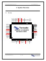
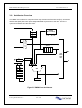
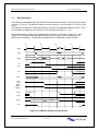
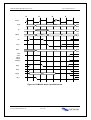
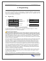
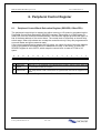
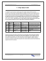
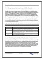
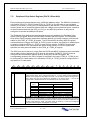
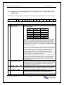
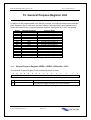
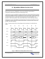
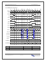
1
IMS16C Embedded Microprocessor User’s Manual V1.11 Infinior MicroSystems MicroSystems’’ IMS16C Tornado ® 16bit Embedded processor User’’s Manual User Infinior ® MicroSystems IMS 16C Last Updated 2003-02-11 1 / 143 IMS16C Embedded Microprocessor User’s Manual V1.11 Infinior Microsystems reserves the right to modify any products described herein at any time without notice in order to improve function or design. Infinior Microsystems does not assume any liability arising from the application or the use of any product described herein; neither does it conveys any license under patent rights nor imply the rights of others. Copyright 2001 - 2002 by Infinior Microsystems: No part of this document may be reproduced in any form or means without the prior written permission of Infinior Microsystems. IMS16C is a registered trademark of Infinior Microsystems. The IMS16C is available from the following manufacturer: Infinior MicroSystems 5F Jeongam Bldg, 769-12, Yeoksam2-Dong, Gangnam-Gu, Seoul, Korea 135-928 Tel: +82-2-6202-5500 FAX: +82-2-6202-5555 www.infinior.com [email protected] 2003-02-10 Last Updated 2003-02-11 applied ERRTA1_2 2 / 143 IMS16C Embedded Microprocessor User’s Manual V1.11 Contents 1. 1.1. 1.2. Introduction .................................................................................................... 6 Overview ............................................................................................................................... 6 IMS16 Families and Road Map............................................................................................. 7 2.1. 2.2. Key Features and Applications ................................................................................................... 9 Key Features....................................................................................................................... 10 Applications......................................................................................................................... 10 3.1. 3.2. 3.3. 3.4. 3.5. 3.6. 3.7. System Overview .................................................................................................. 11 Pin Outs............................................................................................................................... 11 Pin List ................................................................................................................................ 12 Pad Description................................................................................................................... 16 Block Diagram..................................................................................................................... 17 Pin Description .................................................................................................................... 18 Architecture Overview ......................................................................................................... 26 Bus Operation ..................................................................................................................... 27 4.1. 4.2. 4.3. 4.4. 4.5. 4.6. 4.7. 4.8. Programming .................................................................................................. 29 Register Set ........................................................................................................................ 29 Processor Status Flags Register......................................................................................... 30 Memory Organizations and Address Generation................................................................ 31 Segments ............................................................................................................................ 31 Addressing Modes .............................................................................................................. 32 I/O Space ............................................................................................................................ 33 Data Types .......................................................................................................................... 33 Instruction Set ..................................................................................................................... 34 2. 3. 4. 5. Peripherals 6. 6.1. 6.2. 6.3. Peripheral Control Register .................................................................................................. 40 Peripheral Control Block Relocation Register (RELREG, Offset FEh) ............................... 40 Power-Save Control Register (PDCON, Offset F0h) .......................................................... 41 Initializations and Processor Reset..................................................................................... 41 7.1. 7.2. 7.3. 7.4. 7.5. Chip Select Unit .................................................................................................. 42 Upper Memory Chip Select Register (UMCS, Offset A0h) ................................................. 43 Low Memory Chip Select Register (LMCS, Offset A2h) ..................................................... 44 Midrange Memory Chip Select Register (MMCS, Offset A6h)............................................ 45 PCS and MCS Auxiliary Register (MPCS, Offset A8h) ....................................................... 46 Peripheral Chip Select Register (PACS, Offset A4h) .......................................................... 47 7. 8. .................................................................................................. 36 Interrupt Control Unit .................................................................................................. 49 8.1. Definitions of Interrupt Terms .............................................................................................. 49 8.2. Interrupt Conditions and Sequence .................................................................................... 52 8.3. Interrupt Priority................................................................................................................... 53 8.4. Software Exceptions, Traps and NMI.................................................................................. 53 8.5. Fully Nested Mode .............................................................................................................. 55 8.6. Operation in a Polled Environment ..................................................................................... 55 8.7. End-of-Interrupt Write to the EOI Register.......................................................................... 56 8.8. Programmable Priority ........................................................................................................ 56 8.9. Trigger Mode ....................................................................................................................... 56 8.10. Interrupt Control Registers .................................................................................................. 57 Last Updated 2003-02-11 3 / 143 IMS16C Embedded Microprocessor 8.11. 8.12. 8.13. 8.14. 8.15. 8.16. 8.17. 8.18. 8.19. 8.20. 8.21. 8.22. 8.23. 8.24. 9. User’s Manual V1.11 INT0 and INT1 Control Registers (I0CON, Offset 38h, I1CON, Offset 3Ah) (Master Mode) ................................................................................................................................. 58 INT2 and INT3 Control Registers (I2CON, Offset 3Ch, I3CON, Offset 3Eh) (Master Mode) ................................................................................................................................. 59 INT4 Control Register (I4CON, Offset 40h) (Master Mode) ............................................. 60 Timer and DMA Interrupt Control Registers (TCUCON, Offset 32h, DMA0CON, Offset 34h, DMA1CON, Offset 36h) (Master Mode) ........................................................... 61 Watchdog Timer Interrupt Control Register (WDCON, Offset 42h) (Master Mode) ......... 62 UART Serial Interrupt Control Register (U0CON, Offset 44h, U1CON, Offset 46h, U2CON, Offset 48h) (Master Mode) ....................................................................................... 63 Interrupt Status Register (INTSTS, Offset 30h) (Master Mode) ....................................... 64 Interrupt Request Register (REQST, Offset 2Eh) (Master Mode) .................................... 65 In-Service Register (INSERV, Offset 2Ch) (Master Mode)............................................... 66 Priority Mask Register (PRIMSK, Offset 2Ah) (Master Mode) ......................................... 67 Interrupt Mask Register (IMASK, Offset 28h) (Master Mode) .......................................... 68 Poll Status Register (POLLST, Offset 26h) (Master Mode) .............................................. 69 Poll Register (POLL, Offset 24h) (Master Mode) ............................................................. 70 End-of-Interrupt Register (EOI, Offset 22h) (Master Mode) ............................................. 71 Timer Control Unit .................................................................................................. 72 Timer 0 and Timer 1 Mode and Control Registers (T0CON, Offset 56h, T1CON, Offset 5Eh) .......................................................................................................................... 74 9.2. Timer 2 Mode and Control Register (T2CON, Offset 66h).................................................. 75 9.3. Timer Count Registers ( T0CNT, Offset 50h, T1CNT, Offset 58h, T2CNT, Offset 60h ) ..... 76 9.4. Timer Maxcount Compare Registers (T0CMPA, Offset 52h, T0CMPB, Offset 54h, T1CMPA, Offset 5Ah, T1CMPB, Offset 5Ch, T2CMPA, Offset 62h)........................ 77 9.1. 10. DMA Control Unit .................................................................................................. 78 10.1. DMA Operation.................................................................................................................... 79 10.2. DMA Control Registers (D0CON, Offset CAh, D1CON, Offset DAh)............................... 80 10.3. DMA Transfer Count Registers (D0TC, Offset C8h, D1TC, Offset D8h) ............................ 82 10.4. DMA Destination Address High Register (High Order Bits) (D0DSTH, Offset C6h, D1DSTH, Offset D6h) ............................................................................................................... 83 10.5. DMA Destination Address Low Register (Low Order Bits) (D0DSTL, Offset C4h, D1DSTL, Offset D4h) ............................................................................................................... 83 10.6. DMA Source Address High Register (High Order Bits) (D0SRCH, Offset C2h, D1SRCH, Offset D2h) ............................................................................................................... 84 10.7. DMA Source Address Low Register (Low Order Bits) (D0SRCL, Offset C0h, D1SRCL, Offset D0h) ............................................................................................................... 84 10.8. DMA Requests .................................................................................................................... 85 10.9. Synchronization Timing ....................................................................................................... 85 10.10. DMA Acknowledge .............................................................................................................. 87 10.11. DMA Priority ........................................................................................................................ 87 10.12. DMA Programming.............................................................................................................. 87 10.13. DMA Channels on Reset..................................................................................................... 87 11. UART(Asynchronous) Serial Interface ..................................................................................... 88 11.1. PROGRAMMABLE REGISTERS ....................................................................................... 89 11.2. Serial Port Control Register (U0CT, Offset 80h, U1CT, Offset 8Ch, U2CT, Offset 96h) ..... 90 11.3. Serial Port Status Register (U0STS, Offset 82h, U1STS, Offset 8Eh, U2STS, Offset 98h)92 11.4. Serial Port Transmit Data Register (U0TD, Offset 84h, U1TD, Offset 90h, U2TD, Offset 9Ah) .......................................................................................................................... 93 11.5. Serial Port Receive Data Register (U0RD, Offset 86h, U1RD, Offset 92h, U2RD, Offset 9Ch).......................................................................................................................... 93 11.6. Serial Port Baud Rate Divisor Register (U0BAUD, Offset 88h, U1BAUD, Offset 94h, Last Updated 2003-02-11 4 / 143 IMS16C Embedded Microprocessor User’s Manual V1.11 U2BAUD, Offset 96h) ............................................................................................... 94 12. Programmable I/O Unit .................................................................................................. 95 12.1. PIO Mode 2 Register (PIOMODE2, Offset 6Ah) ................................................................. 97 12.2. PIO Mode 1 Register (PIOMODE1, Offset 76h) ................................................................. 97 12.3. PIO Mode 0 Register (PIOMODE0, Offset 70h) ................................................................. 97 12.4. PIO Direction 2 Register (PDIR2, Offset 6Ch) .................................................................... 98 12.5. PIO Direction 1 Register (PDIR1, Offset 78h)..................................................................... 98 12.6. PIO Direction 0 Register (PDIR0, Offset 72h)..................................................................... 98 12.7. PIO Data Register 2 (PDATA2, Offset 6Eh) ........................................................................ 99 12.8. PIO Data Register 1 (PDATA1, Offset 7Ah) ........................................................................ 99 12.9. PIO Data Register 0 (PDATA0, Offset 74h) ........................................................................ 99 13. General Purpose Register Unit .............................................................................................. 100 13.1. General Purpose Register (GPR0 ~ GPR15, Offset 00h ~ 1Eh) ...................................... 100 14. SDRAM Control Unit ................................................................................................ 101 14.1. OVERVIEW OF SDRAM COMMANDS ............................................................................ 103 14.2. Basic Operation................................................................................................................. 106 14.3. Key Features in IMS16C SDRAM Controller .................................................................... 109 14.4. SDRAM Control Register (SDCR, Offset EAh) ................................................................. 110 14.5. SDRAM Auto-refresh Duty Cycle Register (SDDUTY, Offset ECh) ...................................111 14.6. SDRAM Mode Set Register (SDMODE, Offset EEh) ....................................................... 112 15. On-Chip RAM Control Unit ................................................................................................ 113 15.1. On-chip RAM Control Register (SRCR, Offset E8h)......................................................... 114 16. HDLC Controller ................................................................................................ 115 16.1. HDLC Control Register ( HDCTR0, Offset Beh, HDCTR1, Offset B4h ) .......................... 117 16.2. HDLC Status Register ( HDSTR0, Offset BCh, HDSTR1, Offset B2h )............................ 118 16.3. HDLC Transmit Data Buffer Register (TXBFR0, Offset Bah, TXBFR1, Offset B0h)......... 119 16.4. HDLC Receive Data Buffer Register (RXBFR0, Offset B8h, RXBFR1, Offset AEh) ........ 119 16.5. HDLC Baud Rate Divisor Register (BDREG0, Offset B6h, BDREG1, Offset ACh) .......... 120 17. Byte/Word Mode Control Unit ................................................................................................ 121 APPENDIX Last Updated 2003-02-11 ................................................................................................ 122 5 / 143 IMS16C Embedded Microprocessor User’s Manual V1.11 1. Introduction 1.1. Overview Infinior Microsystems is the leading provider of highly integrated IP cores, silicon and system solutions that enable Internet multimedia appliances. Using advanced design methodologies and proprietary technologies, We designs, develops and supplies SOC(System On a Chip) products and leading edge systems for communication markets, mobile computing, digital set-top box, VoIP/VoDSL and embedded networking devices. Infinior Microsystems believes that one of its key competitive advantages is its high performance, highly integrated IP cores based on SOC design technologies encompassing the complete design space from system to silicon. High performance 16bit microcontroller with variety of peripherals like SDRAM controller, MAC controller and HDLC controller still remains instruction level compatible with industry standard x86 microprocessors. The IMS16B microcontroller is performance-enhanced implementations of the industry standard microprocessors with powerful up-to date peripherals such as SDRAM controller. The IMS16C microcontroller is an enhanced version of IMS16B. In addition to IMS16B peripherals, IMS16C microcontroller also has 2 HDLC Controller and Internal 16-kbyte Sync RAM and 16 General Purpose Registers. The IMS16N microcontroller is an enhanced version of IMS16B with 16-Mbyte memory address range. In addition to IMS16B peripherals, IMS16N microcontroller also has MAC Control Unit, HDLC controller and 8-kbyte instruction cache. Last Updated 2003-02-11 6 / 143 IMS16C Embedded Microprocessor 1.2. User’s Manual V1.11 IMS16 Families and Road Map IMS16B IMS16C IMS16N Speed 40/50/60MHz @3.3V 80/90MHz @3.3V 90/100MHz @3.3V Address Bus 20bit 20bit 24bit Data Bus 16bit 16bit 16bit 186/188 mode 186 mode only 186/188 mode 186/188 mode Bus Timing T1, T2, T3, T4 T1, T2, T3 T1, T2, T3 Wait State (UCS, LCS, MCS, PCS) 3, 3, 3, 7 15, 15, 15, 31 15, 15, 15, 31 5V Tolerant I/O No Yes Yes Package 128pin QFP 1420 128pin QFP 1420 144pin QFP Power Consumption 1.65mA/MHz at 3.3V 1.3mA/MHz at 3.3V Deliverable Silicon/IP/Verilog Silicon/IP/Verilog Silicon/IP/Verilog Process 0.5um 0.35um 0.35um Available 1Q 2001 2Q 2002 4Q 2002 UART 1 3 3 DMA Controller 2 External DMA 2 External DMA (2 UART DMA) 2 External DMA (2 UART DMA) SDRAM Controller Yes Yes Yes GPIO 32 pin 44 pin 38 pin Internal GPR No 16bit x 16 General Purpose Register 16bit x 16 General Purpose Register Internal Memory No 16K bytes Sync RAM No Instruction Cache No No 16K bytes WDT S/W H/W H/W Interrupt 6 Ext. /1 NMI 6 Ext. /1 NMI 6 Ext. /1 NMI HDLC Controller No Yes (2 ch) (with 4 x 32bytes FIFO) MAC Controller No No Yes (1 ch) (with 2 x 32bytes FIFO) Yes (10/100 Base T), MII I/F Address Range 1MB 1MB Additional Peripherals Last Updated 2003-02-11 7 / 143 16MB IMS16C Embedded Microprocessor User’s Manual V1.11 IMS16C Last Updated 2003-02-11 8 / 143 IMS16C Embedded Microprocessor User’s Manual V1.11 2. Key Features and Applications The IMS16C is a performance-enhanced implementations of the industry standard AMD Am186EM® microprocessors with powerful up-to date peripherals such as SDRAM controller and two HDLC controllers. This microcontroller integrates the functions of the CPU, nonmultiplexed address bus, timers, chip selects, interrupt controller, DMA controller, 3 asynchronous serial ports, 2 HDLC controllers, 16 general purpose registers, 16kbyte internal memory and 44 programmable I/O pins on one chip. Compared to the existing 16bit microcontrollers, the IMS16C enables system designers to reduce the size, power consumption, and cost of embedded systems, while increasing functionality and performance. Development environments are also widely available. The IMS16C has been totally re-architected from the ground up using the latest design techniques to produce an efficient, high clock-rate CPU core. It provides higher performance than Am186EM and the Intel 80C186 at the same clock frequency. Low power applications not needing this increased performance can run at 1/2 the clock frequency and still obtain more throughputs. The IMS16C has been designed to meet the most common requirements of embedded products developed for the office automation, mass storage, communications and general embedded markets. This device is ideal for use in a broad range of communications applications, including ISDN terminal adapters, low-end routers, digital subscriber line (xDSL) modems, PBX applications, digital phones and key telephone systems. This makes the IMS16C ideal devices for designs requiring high performance, serial communications, and a glueless bus interface to external memory systems. Last Updated 2003-02-11 9 / 143 IMS16C Embedded Microprocessor 2.1. User’s Manual V1.11 Key Features 100% software compatible with the Intel 8086/80186® Supported by widely available native x86 development tools 1Mbyte Memory address space, 64Kbyte I/O space 16-bit ALU IMS16C includes all AMD Am186EM peripherals Peripheral Interface Logic Chip-Select and Ready Control Logic 2 Channel DMA Controllers 3 Programmable 16-bit Timers Interrupt Controller Power Save Logic Chip Select Unit Asynchronous Serial Port Programmable I/O (PIO) 2 HDLC Controllers SDRAM Controller 2 UART Serial Ports with DMA Operation 16k bytes Internal Sync RAM 16 General Purpose Registers 44 General Purpose I/O Pins PLL Management Unit 81.1Mhz, 90.3Mhz, at 3.6864Mhz input clock and x6 Mode Fully synchronous and static design 80/90Mhz operation in 3.3V 0.35um 3.3V CMOS Process (commercial) 3.3V I/O pad (5V tolerant) 128-Pin Quad Flat Pack (QFP 1420) 2.2. Applications General Purpose Applications Toys, Automotive, Instrumentation, Medical, Process and Industrial control PC Peripheral Applications Disk and optical drive storage, Retail and consumer products, Various Peripheral Systems and PCI Add-on cards Telecommunication Applications Fax Machine, ADSL Modem cards, Key phone System Networking Applications VoIP Client, Intelligent Ethernet Hub, SOHO Router Last Updated 2003-02-11 10 / 143 IMS16C Embedded Microprocessor User’s Manual V1.11 3. System Overview Pin Outs XWY XWX XWW `` `_ `^ `] `\ `[ `Z `Y `X `W _` __ _^ _] _\ _[ _Z _Y _X _W ^` ^_ ^^ ^] ^\ ^[ ^Z ^Y ^X ^W ]` ]_ ]^ ]] ]\ {jsrWO[ZP {luWO[YP {WO[XP yjsrWO[WP yluWOZ`P yWOZ_P {jsrXOZ^P {luXOZ]P }zz {XOZ\P yjsrXOZ[P yluXOZZP yXOZYP }kk {typuXOWP {tyv|{XOXP {typuWOXXP {tyv|{WOXWP hyk }kk zykO]P ovsk oskh utp pu{[OZWP }zz pu{Z pu{YOZXP pu{X pu{W z]OY`P zYu zXu zWu {kWOY^P ykWOY_P {kXOYWP ykXOYXP 3.1. XWZ XW[ XW\ XW] XW^ XW_ XW` XXW XXX XXY XXZ XX[ XX\ XX] XX^ XX_ XX` XYW XYX XYY XYZ XY[ XY\ XY] XY^ XY_ Tornado IMS16C LC128QFP9 INFINIOR 2002 hkX\ hkX[ hkXZ hkXY hkXX hkXW hk` hk_ hk^ }zz hk] hk\ hk[ hkZ hkY }kk hkX hkW hsl kluuO\P k{yuO[P ~yu yku hW hX hY }kk hZ h[ h\ h] h^ h_ h` }zz hXW hXX hXY X Y Z [ \ ] ^ _ ` XW XX XY XZ X[ X\ X] X^ X_ X` YW YX YY YZ Y[ Y\ Y] Y^ Y_ Y` ZW ZX ZY ZZ Z[ Z\ Z] Z^ Z_ kyxXOXZP kyxWOXYP zkjzu zkyhzu }zz zkjhzu zk~yu zkih zkkxtX zkkxtW }kk wjz]uOYP wjz\uOZP wjzZuOX`P wjzYuOX_P wjzXuOX^P wjzWuOX]P }kk tjzZuOY\P tjzYuOY[P tjzXuOX\P tjzWuOX[P }zz |jzu sjzu iolu Last Updated 2003-02-11 11 / 143 ][ ]Z ]Y ]X ]W \` \_ \^ \] \\ \[ \Z \Y \X \W [` [_ [^ [] [\ [[ [Z [Y [X [W Z` }zzh }kkh }zzk }kkk {kYOYYP ykYOYZP |puOY]P jsrv|{h ylzl{ i~tvkl }zz Y XOjsrpuP }kk jsrtkX jsrtkW ylzu {lz{tvkl {lz{zl hpvYOhX`PO`P hpvXOhX_PO_P hpvWOhX^PO^P hX] hX\ hX[ hXZ IMS16C Embedded Microprocessor 3.2. User’s Manual V1.11 Pin List Pin No. Pin Name Pad Name Pad Type 1 AD15 PC3B02 IN/OUT 4mA 2 AD14 PC3B02 IN/OUT 4mA 3 AD13 PC3B02 IN/OUT 4mA 4 AD12 PC3B02 IN/OUT 4mA 5 AD11 PC3B02 IN/OUT 4mA 6 AD10 PC3B02 IN/OUT 4mA 7 AD9 PC3B02 IN/OUT 4mA 8 AD8 PC3B02 IN/OUT 4mA 9 AD7 PC3B02 IN/OUT 4mA 10 VSS VSS GROUND 11 AD6 PC3B02 IN/OUT 4mA 12 AD5 PC3B02 IN/OUT 4mA 13 AD4 PC3B02 IN/OUT 4mA 14 AD3 PC3B02 IN/OUT 4mA 15 AD2 PC3B02 IN/OUT 4mA 16 VDD POWER POWER 17 AD1 PC3B02 IN/OUT 4mA 18 AD0 PC3B02 IN/OUT 4mA 19 ALE PC3O02 OUT 4mA 20 DEN_N PC3B02 IN/OUT 4mA 21 DTR_N PC3B02 IN/OUT 4mA 22 WR_N PC3T02 Tri-OUT 4mA 23 RD_N PC3T02 Tri-OUT 4mA 24 A0 PC3T02 Tri-OUT 4mA 25 A1 PC3T02 Tri-OUT 4mA 26 A2 PC3T02 Tri-OUT 4mA 27 VDD VDD POWER 28 A3 PC3T02 Tri-OUT 4mA 29 A4 PC3T02 Tri-OUT 4mA 30 A5 PC3T02 Tri-OUT 4mA 31 A6 PC3T02 Tri-OUT 4mA 32 A7 PC3T02 Tri-OUT 4mA Last Updated 2003-02-11 12 / 143 Pull-up/ Pull-down Driving Current Comments IMS16C Embedded Microprocessor User’s Manual V1.11 Pin No. Pin Name Pad Name Pad Type 33 A8 PC3T02 Tri-OUT 4mA 34 A9 PC3T02 Tri-OUT 4mA 35 VSS VSS GROUND 36 A10 PC3T02 Tri-OUT 4mA 37 A11 PC3T02 Tri-OUT 4mA 38 A12 PC3T02 Tri-OUT 4mA 39 A13 PC3T02 Tri-OUT 4mA 40 A14 PC3T02 Tri-OUT 4mA 41 A15 PC3T02 Tri-OUT 4mA 42 A16 PC3T02 Tri-OUT 4mA 43 AIO0(A17) PC3B02 IN/OUT 4mA 5V Tolerant 44 AIO1(A18) PC3B02 IN/OUT 4mA 5V Tolerant 45 AIO2(A19) PC3B02 IN/OUT 4mA 5V Tolerant 46 TEST_SE PC3D01 INPUT 47 TEST_MODE PC3D01 INPUT 48 RES_N PC3D21U INPUT 49 CLKMD0 PC3D21 INPUT 5V Tolerant 50 CLKMD1 PC3D21 INPUT 5V Tolerant 51 VDD VDD POWER 52 X1(CLKIN) PC3X13 INPUT Oscillator 53 X2 PC3X13 IN/OUT Oscillator 54 VSS VSS GROUND 55 BWMODE PC3D21U INPUT 56 RESET PC3O02 OUT 4mA 57 CLKOUT PC3T02 Tri-OUT 4mA 58 UZI_N PC3B02U IN/OUT Pull-up 4mA 5V Tolerant 59 RXD2 PC3B02U IN/OUT Pull-up 4mA 5V Tolerant 60 TXD2 PC3B02U IN/OUT Pull-up 4mA 61 VDDD VDDD POWER DIGITAL POWER 62 VSSD VDDS GROUND DIGITAL GROUND 63 VDDA VDDA POWER ANALOG POWER 64 VSSA VSSA GROUND ANALOG GROUND Last Updated 2003-02-11 13 / 143 Pull-up/ Pull-down Driving Current Comments 5V Tolerant 5V Tolerant Pull-up 5V Tolerant Pull-up 5V Tolerant 5V Tolerant IMS16C Embedded Microprocessor User’s Manual V1.11 Pin No. Pin Name Pad Name Pad Type Pull-up/ Pull-down Driving Current Comments 65 RXD1 PC3B02U IN/OUT Pull-up 4mA 5V Tolerant 66 TXD1 PC3B02U IN/OUT Pull-up 4mA 5V Tolerant 67 RXD0 PC3B02U IN/OUT Pull-up 4mA 5V Tolerant 68 TXD0 PC3B02U IN/OUT Pull-up 4mA 5V Tolerant 69 S0_N PC3T02 Tri-OUT 4mA 70 S1_N PC3T02 Tri-OUT 4mA 71 S2_N PC3T02 Tri-OUT 4mA 72 S6 PC3B02U IN/OUT Pull-up 73 INT0 PC3D21D INPUT Pull-down 5V Tolerant 74 INT1 PC3D21D INPUT Pull-down 5V Tolerant 75 INT2 PC3B02U IN/OUT Pull-up 4mA 5V Tolerant 76 INT3 PC3B02U IN/OUT Pull-up 4mA 5V Tolerant 77 VSS VSS GROUND 78 INT4 PC3B02U IN/OUT Pull-up 4mA 5V Tolerant 79 NMI PC3D21D INPUT Pull-down 80 HLDA PC3O02 OUT 81 HOLD PC3D21D INPUT 82 SRDY PC3B02 IN/OUT 83 VDD VDD POWER 84 ARDY PC3D21U INPUT Pull-up 5V Tolerant 85 TMROUT0 PC3B02U IN/OUT Pull-up 5V Tolerant 86 TMRIN0 PC3B02U IN/OUT Pull-up 5V Tolerant 87 TMROUT1 PC3B02U IN/OUT Pull-up 5V Tolerant 88 TMRIN1 PC3B02U IN/OUT Pull-up 5V Tolerant 89 VDD VDD POWER 90 RX1 PC3B02U IN/OUT Pull-up 4mA 5V Tolerant 91 RXEN1 PC3B02U IN/OUT Pull-up 4mA 5V Tolerant 92 RXCLK1 PC3B02U IN/OUT Pull-up 4mA 5V Tolerant 93 TX1 PC3B02U IN/OUT Pull-up 4mA 5V Tolerant 94 VSS VSS GROUND 95 TXEN1 PC3B02U IN/OUT Pull-up 4mA 5V Tolerant 96 TXCLK1 PC3B02U IN/OUT Pull-up 4mA 5V Tolerant Last Updated 2003-02-11 14 / 143 4mA 5V Tolerant 5V Tolerant 4mA Pull-down 5V Tolerant 4mA 5V Tolerant IMS16C Embedded Microprocessor Pin No. User’s Manual V1.11 Pin Name Pad Name Pad Type Pull-up/ Pull-down Driving Current Comments 97 RX0 PC3B02U IN/OUT Pull-up 4mA 5V Tolerant 98 RXEN0 PC3B02U IN/OUT Pull-up 4mA 5V Tolerant 99 RXCLK0 PC3B02U IN/OUT Pull-up 4mA 5V Tolerant 100 TX0 PC3B02U IN/OUT Pull-up 4mA 5V Tolerant 101 TXEN0 PC3B02U IN/OUT Pull-up 4mA 5V Tolerant 102 TXCLK0 PC3B02U IN/OUT Pull-up 4mA 5V Tolerant 103 DRQ1 PC3B02U IN/OUT Pull-up 4mA 5V Tolerant 104 DRQ0 PC3B02U IN/OUT Pull-up 4mA 5V Tolerant 105 SD_CS_N PC3O02 OUT 4mA 106 SD_RAS_N PC3O02 OUT 4mA 107 VSS VSS GROUND 108 SD_CAS_N PC3O02 OUT 4mA 109 SD_WR_N PC3O02 OUT 4mA 110 SD_BA PC3O02 OUT 4mA 111 SD_DQM1 PC3O02 OUT 4mA 112 SD_DQM0 PC3O02 OUT 4mA 113 VDD VDD POWER 114 PCS6_N PC3B02U IN/OUT Pull-up 4mA 5V Tolerant 115 PCS5_N PC3B02U IN/OUT Pull-up 4mA 5V Tolerant 116 PCS3_N PC3B02U IN/OUT Pull-up 4mA 5V Tolerant 117 PCS2_N PC3B02U IN/OUT Pull-up 4mA 5V Tolerant 118 PCS1_N PC3B02U IN/OUT Pull-up 4mA 5V Tolerant 119 PCS0_N PC3B02U IN/OUT Pull-up 4mA 5V Tolerant 120 VDD VDD POWER 121 MCS3_N PC3B02U IN/OUT Pull-up 4mA 5V Tolerant 122 MCS2_N PC3B02U IN/OUT Pull-up 4mA 5V Tolerant 123 MCS1_N PC3B02U IN/OUT Pull-up 4mA 5V Tolerant 124 MCS0_N PC3B02U IN/OUT Pull-up 4mA 5V Tolerant 125 VSS VSS GROUND 126 UCS_N PC3T02 Tri-OUT 4mA 127 LCS_N PC3T02 Tri-OUT 4mA 128 BHE_N PC3T02 Tri-OUT 4mA Last Updated 2003-02-11 15 / 143 IMS16C Embedded Microprocessor 3.3. User’s Manual V1.11 Pad Description Pad name Comments PC3X13 3.3V Crystal Oscillator Pads. 40Mhz ~ 100Mhz CLOCK INPUT PC3D01 3.3V CMOS Input Only Pads PC3D31U 3.3V CMOS Input Only Pads With Pull-up Register and Schmitt Trigger non-inverting PC3D21 3.3V CMOS Input Only Pads With Schmitt Trigger non-inverting. PC3D21U 3.3V CMOS Input Only Pads With Pull-up Register and Schmitt Trigger non-inverting. PC3D21D 3.3V CMOS Input Only Pads With Pull-down Register and Schmitt Trigger non-inverting. PC3O02 3.3V CMOS Output Pads with 4mA drive PC3T02 3.3V CMOS 3-State Output Pads with 4mA drive PC3B02 3.3V CMOS 3-State I/O Pads with 4mA drive PC3B02D 3.3V CMOS 3-State I/O Pads With Pull-down Register with 4mA drive PC3B02U 3.3V CMOS 3-State I/O Pads With Pull-up Register with 4mA drive I/O Circuit Pullups Unless otherwise specified, the following current values are used for I/Os with Internal pullup devices. 3.3V Pullup Equivalent resistance Min Current(at Pad = 0 V) -30 uA 88.3 Kohms Max Current (at Pad = 0V) -146 uA 24.7 Kohms I/O Circuit Pulldowns Unless otherwise specified, the following current values are used for I/Os with Internal pulldown devices. Pulldown Equivalent resistance Last Updated 2003-02-11 Min Current (at Pad = 2.65 V) 31 uA 85.5 Kohms 16 / 143 Max Current (at Pad = 3.6V) 159 uA 22.6 Kohms IMS16C Embedded Microprocessor 3.4. User’s Manual V1.11 Block Diagram DRQ0 DRQ1 TMRIN0 TMROUT0 TMRIN1 TMROUT1 LCS_N MCS[3:0]_N UCS_N PCS[6:5]_N PCS[3:0]_N DMA Control Unit Timer Control Unit Chip Select Unit NMI INT[4:0] SD_BA SD_CS_N SD_RAS_N SD_CAS_N SD_WR_N SD_DQM[1:0] Interrupt Control Unit SDRAM Control Unit / GPIO Unit (44) 3 UART Serial Interface Bus Interface Unit ARDY SRDY S[2:0]_N DTR_N DEN_N HOLD HLDA S6 UZI_N PLL Management Unit Control & Execution Unit AIO[2:0] A[16:0] AD[15:0] ALE BHE_N WR_N RD_N Last Updated 2003-02-11 Clock and Power Management Unit VDD GND VDDD VSSD VDDA VSSA X1 X2 RES_N CLKOUT RESET 17 / 143 GPR Unit 2 HDLC Controller Internal 16kbyte Sync RAM CLKMD[1:0] BWMODE TEST_SE TEST_MODE PIO[43:0] *shared RXD0 TXD0 RXD1 TXD1 RXD2 TXD2 TXCLK0 TXEN0 TX0 RXCLK0 RXEN0 RX0 TXCLK1 TXEN1 TX1 RXCLK1 RXEN1 RX1 IMS16C Embedded Microprocessor 3.5. User’s Manual V1.11 Pin Description Pin Name Type Description A16 - A0 Address Bus (3-state output) These pins supply non-multiplexed memory or I/O addresses to the system one-half of a CLKOUT period earlier than the multiplexed address and data bus. During a bus hold or reset condition, the address bus is in a high-impedance state. AIO2 - AIO0 (A19/PIO9, A18/PIO8, A17/PIO7) AD15-AD0 Address, PIO Bus (I/O) These pins are used address A19-A17 and programmable Input/output pin PIO9-PIO7. Address and Data Bus (I/O) These time-multiplexed pins supply partial memory or I/O addresses, as well as data, to the system. This bus supplies the 16bit address to the system during the first period of a bus cycle (t1), and it supplies data to the system during the remaining periods of that cycle (t2 and t3). During a bus hold or reset condition, the address and data bus is in a highimpedance state. ALE Address Latch Enable (output) This pin indicates to the system that an address appears on the address and data bus. The address is guaranteed valid on the trailing edge of ALE. This pin is not three-stated during a bus hold or reset. ARDY Asynchronous Ready (input) This pin indicates to the microcontroller that the addressed memory space or I/O device will complete a data transfer. The ARDY pin accepts a rising edge that is asynchronous to CLKOUT and is active High. The falling edge of ARDY must be synchronized to CLKOUT. To always assert the ready condition to the microcontroller, tie ARDY High. If the system does not use ARDY, tie the pin Low to yield control to SRDY. BHE_N Bus High Enable (3-state output) During a memory access, this pin and the least-significant address bit (AD0 or A0) indicate to the system, which bytes of the data bus (upper, lower, or both) participate in a bus cycle. The BHE_N and AD0 pins are encoded as shown in Table 1. BHE_N is asserted during t1 and remains asserted through t2 and tw . BHE_N does not need to be latched. BHE_N floats during bus hold and reset. BHE_N 0 0 1 1 BWMODE Byte/Word Mode (input) Last Updated 2003-02-11 AD0 0 1 Type of Bus Cycle Word Transfer High Byte Transfer with valid data on Dout(15:8) 0 Low Byte Transfer with valid data on Dout(7:0) 1 Reserved Table 1. Data Byte Encoding IMS16C can be configured either 188 mode(byte mode, bwmode = 0) or 186(word mode, bwmode = 1). When high, ad[15:0] is fully used for IMS16C. When low, ad[7:0] is only used for external data access. 18 / 143 IMS16C Embedded Microprocessor CLKMD0, CLKMD1 Core Clock Mode (input) User’s Manual V1.11 CLKMD0 and CLKMD1 pins determine internal core clock speed. These pins are used for setting PLL frequency coefficients. CLKMD[1:0] 00 01 10 11 Internal Core Clock External clock source bypass mode (1/2) 81.1Mhz core clock with 3.6864Mhz input. Input clock range: 1.9MHz < X1 < 5.5MHz It denotes x22 of Input. 90.3Mhz core clock with 3.6864Mhz input. Input clock range: 1.7 < X1 < 5.1 MHz It denotes x24.5 of Input. External clock x6 Mode. Input clock range: 6.7MHz < X1 < 15MHz Ex) x1 = 11.05Mhz -> core clock = 66.3Mhz Table 2. core clock mode CLKOUT Clock Output (3-state output) This pin is directly connected to inverted internal core clock. It supplies the internal core clock to the system. CLKOUT remains active during reset and bus hold conditions. DEN_N/PIO5 Data Enable (I/O) This pin supplies an output enable to an external data bus transceiver. DEN_N is asserted during memory, I/O, and interrupt acknowledge cycles. DEN_N is deasserted when DTR_N changes state. DEN_N floats during a bus hold or reset condition. DRQ1 - DRQ0 (DRQ1/PIO13, DRQ0/PIO12) DMA Requests (I/O) These pins indicate to the microcontroller that an external device is ready for DMA channel 1 or channel 0 to perform a transfer. DRQ1 - DRQ0 are level-triggered and internally synchronized. The DRQ signals are not latched and must remain active until each serviced(source sync or destination sync). DTR_N/PIO4 Data Transmit or Receive (I/O) This pin indicates which direction data should flow through an external data bus transceiver. When DTR_N is asserted High, the microcontroller transmits data. When this pin is deasserted Low, the microcontroller receives data. DTR_N floats during a bus hold or reset condition. GND Core ground (input) Bus Hold Acknowledge (output) These pins connect the system ground to the IMS16C. Bus Hold Request (input) This pin indicates to the microcontroller that an external bus master needs control of the local bus. The IMS16C microcontroller’ HOLD latency time is a function of the activity occurring in the processor when the HOLD request is received. HLDA HOLD Last Updated 2003-02-11 This pin is asserted High to indicate to an external bus master that the microcontroller has released control of the local bus. When an external bus master requests control of the local bus (by asserting HOLD), the microcontroller completes the bus cycle in progress and then relinquishes control of the bus to the external bus master by asserting HLDA and floating DEN_N, RD_N, WR_N, S2_N - S0_N, AD15 - AD0, S6, A19 - A0, BHE_N and DTR_N, and then driving the chip selects UCS_N, LCS_N, MCS3_N - MCS0_N, PCS6_N - PCS5_N, and PCS3_N PCS0_N High. When the external bus master has finished using the local bus, it indicates this to the microcontroller by deasserting HOLD. The microcontroller responds by deasserting HLDA. 19 / 143 IMS16C Embedded Microprocessor User’s Manual V1.11 INT0 Maskable Interrupt Request 0 (input) This pin indicates to the microcontroller that an interrupt request has occurred. If the INT0 pin is not masked, the microcontroller transfers program execution to the location specified by the INT0 vector in the microcontroller interrupt vector table. Interrupt requests are synchronized internally and can be edgetriggered or level-triggered. To guarantee interrupt recognition, the requesting device must continue asserting INT0 until the request is acknowledged. INT1 Maskable Interrupt Request 1 (input) This pin indicates to the microcontroller that an interrupt request has occurred. If INT1 is not masked, the microcontroller transfers program execution to the location specified by the INT1 vector in the microcontroller interrupt vector table. Interrupt requests are synchronized internally and can be edgetriggered or level-triggered. To guarantee interrupt recognition, the requesting device must continue asserting INT1 until the request is acknowledged. INT2/PIO31 Maskable Interrupt Request 2 (I/O) This pin indicates to the microcontroller that an interrupt request has occurred. If the INT2 pin is not masked, the microcontroller transfers program execution to the location specified by the INT2 vector in the microcontroller interrupt vector table. Interrupt requests are synchronized internally and can be edgetriggered or level-triggered. To guarantee interrupt recognition, the requesting device must continue asserting INT2 until the request is acknowledged. INT3 Maskable Interrupt Request 3 (input) This pin indicates to the microcontroller that an interrupt request has occurred. If the INT3 pin is not masked, the microcontroller then transfers program execution to the location specified by the INT3 vector in the microcontroller interrupt vector table. Interrupt requests are synchronized internally, and can be edgetriggered or level-triggered. To guarantee interrupt recognition, the requesting device must continue asserting INT3 until the request is acknowledged. INT4/PIO30 Maskable Interrupt Request 4 (I/O) This pin indicates to the microcontroller that an interrupt request has occurred. If the INT4 pin is not masked, the microcontroller then transfers program execution to the location specified by the INT4 vector in the microcontroller interrupt vector table. Interrupt requests are synchronized internally, and can be edgetriggered or level-triggered. To guarantee interrupt recognition, the requesting device must continue asserting INT4 until the request is acknowledged. LCS_N Lower Memory Chip Select (output) This pin indicates to the system that a memory access is in progress to the lower memory block. The base address and size of the lower memory block are programmable up to 512 Kbytes. LCS is held High during a bus hold condition. MCS3_N/PIO25 Midrange Memory Chip Select 3 (I/O) This pin indicates to the system that a memory access is in progress to the fourth region of the midrange memory block. The base address and size of the midrange memory block are programmable. MCS3_N is held High during a bus hold condition. MCS2_N - MCS0_N (MCS2/PIO24, MCS1/PIO15, MCS0/PIO14) Midrange Memory Chip Selects (I/O) These pins indicate to the system that a memory access is in progress to the corresponding region of the midrange memory block. The base address and size of the midrange memory block are programmable. Last Updated 2003-02-11 20 / 143 IMS16C Embedded Microprocessor User’s Manual V1.11 MCS2_N - MCS0_N are held High during a bus hold condition. NMI Nonmaskable Interrupt (input) This pin indicates to the microcontroller that an Not maskable interrupt request has occurred. The NMI is the highest priority hardware interrupt pin and, unlike the INT4 - INT0 pins, cannot be masked. The microcontroller always transfers program execution to the location specified by the nonmaskable interrupt vector in the microcontroller interrupt vector table when NMI is asserted. Although NMI is the highest priority interrupt source, it does not participate in the priority resolution process of the maskable interrupts. There is no bit associated with NMI in the interrupt inservice or interrupt request registers. This means that a new NMI request can interrupt an executing NMI interrupt service routine. As with all hardware interrupts, the IF(interrupt enable flag) is cleared when the processor takes the interrupt, disabling the maskable interrupt sources. However, if maskable interrupts are re-enabled by software in the NMI interrupt service routine, via the STI instruction for example, the fact that an NMI is currently in service will not have any effect on the priority resolution of maskable interrupt requests. For this reason, it is strongly advised that the interrupt service routine for NMI should not enable the maskable interrupts. An NMI transition from Low to High is latched and synchronized internally, and it initiates the interrupt at the next instruction boundary. To guarantee that the interrupt is recognized, the NMI pin must be asserted for at least one CLKOUT period. PCS3_N - PCS0_N (PCS3_N/PIO19, PCS2_N/PIO18, PCS1_N/PIO17, PCS0_N/PIO16) Peripheral Chip Selects (I/O) These pins indicate to the system that a peripheral access is in progress to the corresponding region(either I/O or memory address space). The base address of the peripheral memory block is programmable. PCS3_N - PCS0_N are held High during a bus hold condition. They are also held High during reset. Unlike the UCS_N and LCS_N chip selects, the PCS_N outputs assert with the multiplexed AD address bus. Note also that each peripheral chip select asserts over a 256byte address range, which is twice the address range covered by peripheral chip selects in the 80C186 and 80C188 microcontrollers. PCS5_N/A1/PIO3 Peripheral Chip Select 5, Latched Address Bit 1 (I/O) PCS5_N: These pins indicate to the system that a peripheral access is in progress to the corresponding region(either I/O or memory address space). The base address of the peripheral memory block is programmable. PCS5_N is held High during a bus hold condition. It is also held High during reset. Unlike the UCS_N and LCS_N chip selects, the PCS_N outputs assert with the multiplexed AD address bus. Note also that each peripheral chip select asserts over a 256 byte address range, which is twice the address range covered by peripheral chip selects in the 80C186. A1: When the EX bit in the MCS_N and PCS_N auxiliary register is 0, this pin supplies an internally latched address bit 1 to the system. During a bus hold condition, A1 retains its previously latched value. PCS6_N/A2/PIO2 Peripheral Chip Select 6, Latched Address Bit 2 (I/O) PCS6_N: These pins indicate to the system that a peripheral access is in progress to the corresponding region(either I/O or memory address space). The base address of the peripheral memory Last Updated 2003-02-11 21 / 143 IMS16C Embedded Microprocessor User’s Manual V1.11 block is programmable. PCS6_N is held High during a bus hold condition or reset. Unlike the UCS_N and LCS_N chip selects, the PCS outputs assert with the multiplexed AD address bus. Note also that each peripheral chip select asserts over a 256 byte address range, which is twice the address range covered by peripheral chip selects in the 80C186. A2: When the EX bit in the MCS and PCS Auxiliary Register is 0, this pin supplies an internally latched address bit 2 to the system. During a bus hold condition, A2 retains its previously latched value. PIO43 - PIO0 (Shared) Programmable I/O Pins The IMS16C microcontroller provides 44 individually programmable I/O pins. Each PIO can be programmed with the following attributes: PIO function (enabled/disabled), direction (input/output). The pins that are multiplexed with PIO43 - PIO0 are listed in Table 3. After power-on reset, the PIO pins default to various configurations. The column titled Power-On Reset Status in Table 3 lists the defaults for the PIOs. The system initialization code must reconfigure any PIOs as required. The A19 - A17(AIO2 –AIO0) address pins default to normal operation on power-on reset, allowing the processor to correctly begin fetching instructions at the boot address FFFF0h. The DTR_N, DEN_N, and SRDY pins also default to normal operation on power-on reset. PIO 0 1 2 3 4 5 6 7 8 9 10 11 12 13 14 15 16 17 18 19 20 21 22 23 24 25 26 27 28 Last Updated 2003-02-11 22 / 143 Associated TMRIN1 TMROUT1 PCS6_N PCS5_N DTR_N DEN_N SRDY AIO0(A17) AIO1(A18) AIO2(A19) TMROUT0 TMRIN0 DRQ0 DRQ1 MCS0_N MCS1_N PCS0_N PCS1_N PCS2_N PCS3_N TXD1 RXD1 TXD2 RXD2 MCS2_N MCS3_N UZI_N TXD0 RXD0 Power-On Reset Status Input with pullup Input with pullup Input with pullup Input with pullup Normal operation Normal operation Normal operation Normal operation Normal operation Normal operation Input with pullup Input with pullup Input with pullup Input with pullup Input with pullup Input with pullup Input with pullup Input with pullup Input with pullup Input with pullup Input with pullup Input with pullup Input with pullup Input with pullup Input with pullup Input with pullup Input with pullup Input with pullup Input with pullup IMS16C Embedded Microprocessor User’s Manual V1.11 28 29 30 31 32 33 34 35 36 37 38 39 40 41 42 43 VDDA, VSSA RXD0 Input with pullup S6 Input with pullup INT4 Input with pullup INT2 Input with pullup RX1 Input with pullup RXEN1 Input with pullup RXCLK1 Input with pullup TX1 Input with pullup TXEN1 Input with pullup TXCLK1 Input with pullup RX0 Input with pullup RXEN0 Input with pullup RXCLK0 Input with pullup TX0 Input with pullup TXEN0 Input with pullup TXCLK0 Input with pullup Table 3. Numeric PIO Pin Assignments Analog vdd, vss (input) Digital vdd, vss (input) Reset out (output) PLL Core Analog power supply and ground RD_N Read Strobe (3-state output) This pin indicates to the system that the microcontroller is performing a memory or I/O read cycle. RD_N pin is guaranteed not to be asserted before the address and data bus is floated during the address-to-data transition. RD_N floats during a bus hold condition RES_N Reset (input) This pin requires the microcontroller to perform a reset. When RES_N is asserted, the microcontroller immediately terminates its present activity, clears its internal logic, and CPU control is transferred to the reset address FFFF0h. RES_N must be held Low for at least 1 ms. RES_N can be asserted asynchronously to CLKOUT because RES_N is synchronized internally. For proper initialization, VCC must be within specifications, and CLKOUT must be stable for more than ten CLKOUT periods during which RES_N is asserted. This input is provided with Schmitt trigger to facilitate power-on reset generation via an RC network. RX0/PIO38 RX1/PIO32 HDLC Receive Data (I/O) This pin supplies HDLC serial receive data from the system to the internal HDLC controller. RXEN0/PIO39 RXEN1/PIO33 HDLC Receive Enable (I/O) HDLC Receive Clock (I/O) This pin controls HDLC serial receive data from the system to the internal HDLC controller. UART Receive Data (I/O) This pin supplies UART serial receive data from the system to the internal UART controller. Especially, RXD0, RXD1 can be configured to DMA operation. Otherwise RXD2 is restricted to normal UART operation only. VDDD, VSSD RESET RXCLK0/PIO40 RXCLK1/PIO34 RXD0/PIO28 RXD1/PIO21 RXD2/PIO23 Last Updated 2003-02-11 PLL Core Digital power supply and ground Reset Output indicates that the CPU is being reset, and can be used as a system reset, It is active high, synchronized with the processor clock, and lasts an integer number of clock periods corresponding to the length of the RES_N signal. This pin supplies HDLC serial receive data sync clock to the system or receives serial data sync clock from the system. 23 / 143 IMS16C Embedded Microprocessor S2_N - S0_N Bus Cycle Status (3-state output) User’s Manual V1.11 These pins indicate to the system the type of bus cycle in progress. S2_N can be used as a logical memory or I/O indicator, and S1_N can be used as a data transmit or receive indicator. S2_N - S0_N float during bus hold and hold acknowledges conditions. The S2_N - S0_N pins are encoded as shown in Table 4. S2_N 0 0 0 0 1 1 1 1 S1_N S0_N Bus Cycle 0 0 Interrupt acknowledge 0 1 Read data from I/O 1 0 Write data to I/O 1 1 Halt 0 0 Instruction fetch 0 1 Read data from memory 1 0 Write data to memory 1 1 No Bus Activity Table 4. Bus Cycle Encoding S6/PIO29 Bus Cycle Status Bit 6 (I/O) During the second and remaining periods of a cycle (t2 and t3), this pin is asserted High to indicate a DMA-initiated bus cycle. During a bus hold or reset condition, S6 floats. If S6 is to be used as PIO29 in input mode, the device driving PIO29 must not drive the pin Low during power-on reset. S6/PIO29 defaults to a PIO input with pullup, so the pin does not need to be driven High externally. TEST_SE Scan enable (input) Scan test (input) SDRAM control (output) SDRAM control (output) SDRAM control (output) SDRAM control (output) SDRAM control (output) SDRAM control (output) Synchronous Ready (I/O) TEST_SE pin is used for scan test. Active high. TMRIN0/PIO11 Timer Input 0 (I/O) This pin supplies a clock or control signal to the internal microcontroller timer 0. After internally synchronizing a Low-toHigh transition on TMRIN0, the microcontroller increments the timer. TMRIN0 must be tied High if not being used. TMRIN1/PIO0 Timer Input 1 (I/O) This pin supplies a clock or control signal to the internal microcontroller timer 1. After internally synchronizing a Low-toHigh transition on TMRIN1, the microcontroller increments the timer. TMRIN1 must be tied High if not being used. TEST_MODE SD_BA SD_CS_N SD_CAS_N SD_LAS_N SD_WR_N SD_DQM1 SD_DQM0 SRDY/PIO6 Last Updated 2003-02-11 TEST_MODE pin is used for scan test. Active high. This is the bank selection pin connected to the SDRAM This is the active low SDRAM chip select pin. This is the active low SDRAM column address select pin. This is the active low SDRAM low address select pin. This is the active low SDRAM write pin. This is the active high byte mask signal. When high, no data can be read to written to the SDRAM. This pin indicates to the microcontroller that the addressed memory space or I/O device will complete a data transfer. The SRDY pin accepts an active High input synchronized to CLKOUT. Using SRDY instead of ARDY allows relaxed system timing because of the elimination of the one-half clock period required to internally synchronize ARDY. To always assert the ready condition to the microcontroller, tie SRDY High. If the system does not use SRDY, tie the pin Low to yield control to ARDY. 24 / 143 IMS16C Embedded Microprocessor User’s Manual V1.11 TMROUT0/PIO10 Timer Output 0 (I/O) This pin supplies the system with either a single pulse or a continuous waveform with a programmable duty cycle. TMROUT0 is floated during a bus hold or reset. TMROUT1/PIO1 Timer Output 1 (I/O) This pin supplies the system with either a single pulse or a continuous waveform with a programmable duty cycle. TMROUT1 can also be programmed as a watchdog timer. TMROUT1 is floated during a bus hold or reset. TXD0/PIO27 TXD1/PIO20 TXD2/PIO22 Transmit Data (I/O) This pin supplies UART serial transmit data to the system from the internal UART controller. Especially, TXD0, TXD1 can be configured to DMA operation. Otherwise TXD2 is restricted to normal UART operation only. TX0/PIO41 TX1/PIO35 Transmit Data (I/O) This pin supplies HDLC serial transmit data from the system to the internal HDLC controller. TXEN0/PIO42 TXEN1/PIO36 Transmit Enable (I/O) This pin controls HDLC serial transmit data from the system to the internal HDLC controller. TXCLK0/PIO43 TXCLK1/PIO37 Transmit Clock (I/O) This pin supplies HDLC serial transmit data sync clock to the system or receives serial data sync clock from the system. UCS_N Upper Memory Chip Select (output) This pin indicates to the system that a memory access is in progress to the upper memory block. The base address and size of the upper memory block are programmable up to 512 Kbytes. UCS is held High during a bus hold condition. After power-on reset, UCS is asserted because the processor begins executing at FFFF0h and the default configuration for the UCS chip select is 64 Kbytes from F0000h to FFFFFh. UZI_N/PIO26 Upper Zero Indicate (I/O) This pin lets the designer determine if an access to the interrupt vector table is in progress by ORing it with bits 15-10 of the address and data bus. UZI is the logical OR of the inverted A19 A16 bits, and it asserts in the first period of a bus cycle and is held throughout the cycle. VDD Digital Power supply (input) Write Strobe (3-state output) Digital Power Supply X1(CLKIN) Crystal Input (input) This pin and the X2 pin provide connections for a fundamental mode or third-overtone parallel-resonant crystal used by the internal oscillator circuit. To provide the microcontroller with an external clock source, connect the source to the X1 pin and leave the X2 pin unconnected. X2 Crystal Output (output) This pin and the X1 pin provide connections for a fundamental mode or third-overtone parallel-resonant crystal used by the internal oscillator circuit. To provide the microcontroller with an external clock source, leave the X2 pin unconnected and connect the source to the X1 pin. WR_N Last Updated 2003-02-11 This pin indicates to the system that the data on the bus is to be written to a memory or I/O device. WR_N floats during a bus hold or reset condition 25 / 143 IMS16C Embedded Microprocessor 3.6. User’s Manual V1.11 Architecture Overview The IMS86 core in IMS16C is comprised of two major functions the Execution Unit (EU), and the Bus Interface Unit (BIU). Both units operate independent and asynchronous to the other. The EU is responsible for instruction execution and effective address calculations. The BIU performs all bus cycles and maintains the instruction queue. DECODER (Main Control Block) CS DS SS ES A D D E R 6 byte Instruction Queue hG BUS INTER FACE UNIT IP hkG hk G AH AL CH CL DH DL BH BL ALU SP BP SI DI FLAG Figure 3.5 IMS86 Core Architecture Last Updated 2003-02-11 26 / 143 IMS16C Embedded Microprocessor 3.7. User’s Manual V1.11 Bus Operation The industry-standard 80C186 and 80C188 microcontrollers finishes 1 bus cycle with 4 clock cycles(t1, t2, t3, t4). The IMS16C reduces 4 clock cycles to 3 clock cycles(t1, t2, t3) for 1 bus cycle. The IMS16C provides the multiplexed AD bus and a non-multiplexed address (A) bus. The A bus provides an address to the system for the complete bus cycle (t1 – t3). Read and write bus cycles can be performed to memory or I/O space. Figure 3.6.1 and Figure 3.6.2 shows the affected signals during a normal read or write operation for an IMS16C microcontroller. The address and data will be multiplexed onto the AD bus. t3 t1 t2 CLKOUT tw A[19:0] AD[15:0] t3 h k h ALE RD_N RDY BHE_N iolu LCS_N, UCS_N MCS1_N MCS0_N PCS[6:0]_N DEN_N DTR_N S[2:0]_N Status Status UZI_N Figure 3.6.1 IMS16C Read Cycle Waveforms Last Updated 2003-02-11 27 / 143 IMS16C Embedded Microprocessor t3 User’s Manual V1.11 t1 t2 CLKOUT t3 tw A[19:0] Address S6 S6 AD[15:0] Address DATA ALE WR_N BHE_N BHE_N LCS_N UCS_N MCS1_N MCS0_N PCS[6:0]_N DEN_N DTR_N S[2:0]_N Status UZI_N Figure 3.6.2 IMS16C Write Cycle Waveforms Last Updated 2003-02-11 28 / 143 IMS16C Embedded Microprocessor User’s Manual V1.11 4. Programming All members of the IMS16 series microprocessors, including the IMS16C, contain the same basic set of registers, instructions, and addressing modes, and are compatible with the original industry-standard 186/188 parts. 4.1. Register Set 15 AX DX CX BX BP SI DI SP 8 7 0 AH AL DH DL CH CL BH BL Base Pointer Source Index Destination Index Stack Pointer 15 0 Multiply/Divide I/O Instructions Loop/Shift/Repeat/Count Base Registers CS DS SS ES Code Segment Data Segment Stack Segment Extra Segment Segment Registers Index Registers Stack Pointer General Purpose registers F IP Processor Status Flags Instruction Pointer Status & Control Registers Figure 4.1 Programming Model The base architecture of the IMS16C has 14 registers, as shown in Figure 4.1. These registers are grouped into the following categories: General Purpose Registers Eight 16-bit general purpose registers can be used for arithmetic and logical operands. Four of these (AX, BX, CX, and DX) can be used as 16-bit registers or split into pairs of separate 8-bit registers (AH, AL, BH, BL, CH, CL, DH, and DL). The Destination Index (DI) and Source Index (SI) registers are used for data movement and string instructions. The Base Pointer (BP) and Stack Pointer (SP) registers are used for the stack segment and point to the bottom and top of the stack, respectively. Some of the general purpose registers also have dedicated functions with certain instructions as noted in Figure 4.1. The AX and DX registers are used during multiply, divide and I/O instructions. The CX register is used during instructions that have a repeat count for loop, shift and repeat. BX and BP can be used as base pointers used during effective address calculations. SI and DI can be used as index registers during effective address calculations. Four of the general-purpose registers (BP, BX, DI, and SI) can also be used to determine offset addresses of operands in memory. These registers can contain base addresses or indexes to particular locations within a segment. The addressing mode selects the specific registers for operand and address calculations. All stack operations (POP, POPA, POPF, PUSH, PUSHA, PUSHF) utilize the stack pointer. The Stack Pointer register is always offset from the Stack Segment (SS) register, and no segment override is allowed. Besides, The IMS16C has 16 word Memory Mapped General Purpose Registers. It locates Last Updated 2003-02-11 29 / 143 IMS16C Embedded Microprocessor User’s Manual V1.11 I/O memory space ranges from FF00h to FF1Eh. Users can access these registers using IN, OUT instructions. Segment Registers Four 16-bit special-purpose registers (CS, DS, ES, and SS) select, at any given time, the segments of memory that are immediately addressable for code (CS), data (DS and ES), and stack (SS) memory. CS is used for instruction prefetch and immediate data. DS is used for all other data references. SS is used for all stack pushes and pops; any memory reference that uses BP as a base register. ES is used for all string instruction references that use the DI register as an index. Status and Control Registers Two 16bit special purpose registers record or alter certain aspects of the processor state. The Instruction Pointer (IP) register contains the offset address of the next sequential instruction to be executed and the Processor Status Flags (FLAGS) register contains status and control flag bits. 4.2. Processor Status Flags Register The 16-bit processor Status Flags register records specific characteristics of the result of logical and arithmetic instructions and controls the operation of the microcontroller within a given operating mode. After an instruction is executed, the value of the flags may be set, cleared/reset, unchanged, or undefined. The term undefined means that the flag value prior to the execution of the instruction is not preserved, and the value of the flag after the instruction is executed cannot be predicted. 15 14 13 12 11 10 OF DF 9 IF 8 7 6 TF SF ZF 5 4 AF 3 2 PF 1 0 CF Bit Name Function 11 Overflow Flag 10 Direction Flag 9 InterruptEnable Flag Trace Flag Set if the signed result cannot be expressed within the number of bits in the destination operand, cleared otherwise Used during string instructions to determine auto decrement(DF=1), or auto increment (DF=0) of index value. When set, enables maskable interrupts to cause the CPU to transfer control to a location specified by an interrupt vector. When set, a trace interrupt occurs after instructions execute. TF is cleared by the trace interrupt after the processor status flags are pushed onto the stack. The trace service routine can continue tracing by popping the flags back with an interrupt return (IRET) instruction. Set equal to high-order bit of result (0 if 0 or positive, 1 if negative). Set if result is 0; cleared otherwise. Set on carry from or borrow to the low-order 4 bits of the AL general-purpose register; cleared otherwise. Set if low-order 8 bits of result contain an even number of 1’s; cleared otherwise. Set on high-order bit carry or borrow; cleared otherwise. 8 7 6 4 2 0 Sign Flag Zero Flag Auxiliary Carry Parity Flag Carry Flag Figure 4.2 Status Flags Register Last Updated 2003-02-11 30 / 143 IMS16C Embedded Microprocessor 4.3. User’s Manual V1.11 Memory Organizations and Address Generation Memory is organized in sets of segments. Each segment is a linear contiguous sequence of 64K (216 ) 8-bit bytes. Memory is addressed using a two-component address that consists of a 16-bit segment value and a 16-bit offset. The offset is the number of bytes from the beginning of the segment (the segment address), to the data or instruction that is being accessed. The processor forms the physical address of the target location by taking the segment address, shifting it to the left 4 bits (multiplying by 16), and adding this to the 16-bit offset. The result is the 20-bit address of the target data or instruction. This allows for a 1-Mbyte physical address size. Figure 4.3 shows physical address generation example. Physical Address Logical Address W X`G Shift Left 4 Bits Zero Extended Add 1 0 1 2 3 4 0 5 6 7 7 9 B 8 8 X\G WG 1 2 3 4 5 6 7 8 Segment Base Offset To Memory Figure 4.3 Physical Address Generation 4.4. Segments The IMS16C uses four segment registers: 1. Data Segment (DS): The processor assumes that all accesses to the program’s variables are from the 64K space pointed to by the DS register. The data segment holds data, operands, etc. 2. Code Segment (CS): This 64K space is the default location for all instructions. All code must be executed from the code segment. 3. Stack Segment (SS): The processor uses the SS register to perform operations that involve the stack, such as pushes and pops. The stack segment is used for temporary space. 4. Extra Segment (ES): Usually this segment is used for large string operations and for large data structures. Certain string instructions assume the extra segment as the segment portion of the address. The extra segment is also used (by using segment override) as a spare data segment. When a segment is not defined for a data movement instruction, it’s assumed to be a data segment. An instruction prefix can be used to override the segment register. For speed and compact instruction encoding, the segment register used for physical address generation is implied by the addressing mode used (see Figure 4.4). Last Updated 2003-02-11 31 / 143 IMS16C Embedded Microprocessor User’s Manual V1.11 Memory Reference Needed Segment Register Used Implicit Segment Selection Rule Local Data Instructions Stack Data(DS) Code(CS) Stack(SS) External Data(Global) Extra(ES) All data references Instructions, Immediate data All stack pushes and pops Any memory references that use the BP register All string instruction references that use the DI register as an index Figure 4.4 Segment Register Selection Rules 4.5. Addressing Modes The IMS16C microcontroller uses eight categories of addressing modes to specify operands. - Two addressing modes are provided for instructions that operate on register or immediate operands. - Six addressing modes are provided to specify the location of an operand in a memory segment. Register and Immediate Operands Register Operand Mode : The operand is located in one of the 8- or 16-bit registers. Immediate Operand Mode :The operand is included in the instruction. Memory Operands A memory-operand address consists of two 16-bit components: a segment value and an offset. The segment value is supplied by a 16 bit segment register either implicitly chosen by the addressing mode or explicitly chosen by a segment override prefix. The offset, also called the effective address, is calculated by summing any combination of the following three address elements: 1. Displacement : an 8-bit or 16-bit immediate value contained in the instruction 2. Base : contents of either the BX or BP base registers 3. Index : contents of either the SI or DI index registers Any carry from the 16-bit addition is ignored. Eight-bit displacements are sign-extended to 16-bit values. Combinations of the above three address elements define the following six memory addressing modes: BX BP None + SI 8bit DI + 16bit None None 1. Direct Mode : The operand offset is contained in the instruction as an 8- or 16-bit displacement element. 2. Register Indirect Mode : The operand offset is in one of the registers BP, BX, DI, or SI. 3. Based Mode : The operand offset is the sum of an 8- or 16-bit displacement and the contents of a base register (BX or BP). 4. Indexed Mode : The operand offset is the sum of an 8- or 16-bit displacement and the contents of an index register (DI or SI). Last Updated 2003-02-11 32 / 143 IMS16C Embedded Microprocessor User’s Manual V1.11 5. Based Indexed Mode : The operand offset is the sum of the contents of a base register (BP or BX) and an index register (DI or SI). 6. Based Indexed Mode with Displacement : The operand offset is the sum of a base register’s contents, an index register’s contents, and an 8-bit or 16-bit displacement. Addressing Mode Example Direct Register Indirect Based Indexed Based Indexed Based Indexed with displacement mov ax, ds:4 mov ax, [si] mov ax, [bx]4 mov ax, [si]4 mov ax, [si][bx] mov ax, [si][bx]4 Figure 4.5 Memory Addressing Mode Examples 4.6. I/O Space The I/O space consists of 64K 8-bit or 32K 16-bit ports. The IN and OUT instructions address the I/O space with either an 8-bit port address specified in the instruction, or a 16-bit port address in the DX register. Eight-bit port addresses are zero-extended so that A15–A8 are Low. I/O port addresses 00F8h through 00FFh are reserved. 1Mbyte Memory Space Memory or I/O 64Kbyte I/O Space Figure 4.6 Memory and I/O Space 4.7. Data Types The IMS16C supports the following data types: Integer A signed binary numeric value contained in an 8-bit byte or a 16-bit word. All operations assume a two’s complement representation. Ordinal An unsigned binary numeric value contained in an 8-bit byte or a 16-bit word. Double Word A signed binary numeric value contained in two sequential 16-bit addresses, or in a DX::AX register pair. Quad Word A signed binary numeric value contained in four sequential 16-bit addresses. BCD An unpacked byte representation of the decimal digits 0-9. ASCII A byte representation of alphanumeric and control characters using the ASCII standard of character representation. Last Updated 2003-02-11 33 / 143 IMS16C Embedded Microprocessor User’s Manual V1.11 Packed BCD A packed byte representation of two decimal digits (0-9). One digit is stored in each nibble (4 bits) of the byte. String A contiguous sequence of bytes or words. A string can contain from 1 byte up to 64 Kbytes. Pointer 16-bit or 32-bit quantities composed of a 16-bit offset component or a 16-bit segment base component plus a 16-bit offset component. In general, individual data elements must fit within defined segment limits. 4.8. Instruction Set This chapter contains descriptions of the brief overview of IMS16C Instruction set constitution. The IMS16C shares the standard 186 instruction set. An instruction can reference from zero to several operands. An operand can reside in a register, in the instruction itself, or in memory. OPCODE w 1 byte or 2bytes mod reg r/m (disp-low) (disp-high) 8bit or 16bit displacement if memory operand needs. (data) (data) 8bit or 16bit immediate data mod r/m 00 01 000 001 010 011 100 101 110 111 (BX) + (SI) (BX) + (DI) (BP) + (SI) (BP) + (DI) (SI) (DI) DIRECT (BX) + [DI] (BX) + (SI) + D8 (BX) + (DI) + D8 (BP) + (SI) + D8 (BP) + (DI) + D8 (SI) + D8 (DI) + D8 (BP) + D8 (BX) + D8 reg w=0 w=1 000 001 010 011 100 101 110 111 AL CL DL BL AH CH DH BH AX CX DX BX SP BP SI DI 10 11 (BX) + (SI) + D16 (BX) + (DI) + D16 (BP) + (SI) + D16 (BP) + (DI) + D16 (SI) + D16 (DI) + D16 (BP) + D16 (BX) + D16 w=0 AL CL DL BL AH CH DH BH w=1 AX CX DX BX SP BP SI DI Segment Register Code ES CS SS DS 00 01 10 11 AAA ASCII adjust for addition AAD ASCII adjust for division AAM ASCII adjust for multiplication AAS ASCII adjust for subtraction ADC Add byte or word with carry ADD Add byte or word AND Logical AND byte or word BOUND Detects values outside prescribed range Last Updated 2003-02-11 34 / 143 IMS16C Embedded Microprocessor User’s Manual V1.11 CALL Call procedure CBW Convert byte to word CLC Clear carry flag CLD Clear direction flag CLI Clear interrupt-enable flag CMC Complement carry flag CMP Compare byte or word CMPS Compare byte or word string CWD Convert word to double word DAA Decimal adjust for addition DAS Decimal adjust for subtraction DEC Decrement byte or word by 1 DIV Divide byte or word unsigned ENTER Format stack for procedure entry ESC Escape to extension processor HLT Halt until interrupt or reset IDIV Integer divide byte or word IMUL Integer multiply byte or word IN Input byte or word INC Increment byte or word by 1 INS Input bytes or word string INT Interrupt INTO Interrupt if overflow IRET Interrupt return JA/JNBE Jump if above/not below or equal JAE/JNB Jump if above or equal/not below JB/JNAE Jump if below/not above or equal JBE/JNA Jump if below or equal/not above JC Jump if carry JCXZ Jump if register CX = 0 JE/JZ Jump if equal/zero JG/JNLE Jump if greater/not less or equal JGE/JNL Jump if greater or equal/not less JL/JNGE Jump if less/not greater or equal JLE/JNG Jump if less or equal/not greater JMP Jump JNC Jump if not carry JNE/JNZ Jump if not equal/not zero JNO Jump if not overflow JNP/JPO Jump if not parity/parity odd JNS Jump if not sign JO Jump if overflow JP/JPE Jump if parity/parity even JS Jump if sign LAHF Load AH register from flags LDS Load pointer using DS LEA Load effective address LEAVE Restore stack for procedure exit LES Load pointer using ES LOCK Lock bus during next instruction LODS Load byte or word string LOOP Loop LOOPE/ LOOPZ MOV Loop if equal/zero Loop if not equal/not zero Move byte or word LOOPNE/ LOOPNZ MOVS MUL Multiply byte or word unsigned NEG Negate byte or word NOP No operation NOT Logical NOT byte or word OR Logical Inclusive OR byte or word OUT Output byte or word POP Pop word off stack POPA Pop all general register off stack POPF Pop flags off stack PUSH Push word onto stack PUSHA Push all general registers onto stack PUSHF Push flags onto stack RCL Rotate left through carry byte or word RCR Rotate right through carry byte or word REP Repeat REPE/REPZ Repeat while equal/zero REPNE/ REPNZ ROL Repeat while not equal/not zero RET0 Return from procedure Rotate left byte or word ROR Rotate right byte or word SAHF SAL Shift left arithmetic byte or word SAR Store AH register in flags SF, ZF, AF, PF, and CF Shift right arithmetic byte or word SBB Subtract byte or word with borrow SCAS Scan byte or word string SHL Shift left logical byte or word SHR Shift right logical byte or word STC Set carry flag STD Set direction flag STI Set interrupt-enable flag STOS Store byte or word string SUB Subtract byte or word TEST Test (Logical AND, flags only set) byte or word Translate byte XCHG Exchange byte or word XOR Logical exclusive OR byte or word XLAT Move byte or word string Figure 4.8 Major Instruction Set of IMS16C Last Updated 2003-02-11 35 / 143 IMS16C Embedded Microprocessor User’s Manual V1.11 5. Peripherals This section documents the operation of the IMS16C integrated peripherals. The IMS16C includes the following peripherals: Peripheral Interface Logic Power-Save Logic Chip-Select and Ready Control Logic 2 Channel DMA controllers 3 Programmable 16-bit Timers Interrupt Controller 3 UART Controllers 2 HDLC Controllers SDRAM Controller Two 8kbytes Single port Sync RAM The peripheral control block can be mapped into either memory or I/O space. The base address of the control block must be on an even 256-byte boundary (i.e., the lower eight bits of the base address are 00h). Internal logic recognizes control block addresses and responds to bus cycles. During bus cycles to internal registers, the bus controller signals the operation externally (i.e., the RD, WR, status, address, and data lines are driven as in a normal bus cycle), but the data bus, SRDY, and ARDY are ignored. At reset, the Peripheral Control Block Relocation register is set to 00FFh, which maps the control block to start at FF00h in I/O space. An offset map of the 256-byte peripheral control register block is shown in Figure 5 Offset (hex) Register Name FE FC FA F8 F6 F4 F2 F0 Peripheral Control Block Relocation Register EE EC EA E8 E6 E4 E2 E0 SDRAM Mode Set Register SDRAM Auto Refresh Duty Cycle Register SDRAM Enable Register Internal Sync RAM 8kw Enable Register Processor Release Level Register Power-Save Control Register DE DC Last Updated 2003-02-11 36 / 143 IMS16C Embedded Microprocessor User’s Manual V1.11 DA D8 D6 D4 D2 D0 DMA 1 Control Register DMA 1 Transfer Count Register DMA1 Destination Address High Register DMA 1 Destination Address Low Register DMA 1 Source Address High Register DMA 1 Source Address Low Register CE CC CA C8 C6 C4 C2 C0 DMA 0 Control Register DMA 0 Transfer Count Register DMA0 Destination Address High Register DMA 0 Destination Address Low Register DMA 0 Source Address High Register DMA 0 Source Address Low Register BE BC BA B8 B6 B4 B2 B0 HDLC 0 Control Register HDLC 0 Status Register HDLC 0 Tx Buffer Register HDLC 0 Rx Buffer Register HDLC 0 Buad Register HDLC 1 Control Register HDLC 1 Status Register HDLC 1 Tx Buffer Register AE AC AA A8 A6 A4 A2 A0 HDLC 1 Rx Buffer Register HDLC 1 Buad Register PCS_N and MCS_N Auxiliary Register Midrange Memory Chip Select Register Peripheral Chip Select Register Lower Memory Chip Select Register Upper Memory Chip Select Register 9E 9C 9A 98 96 94 92 90 UART 2 Baud Rate Divisor Register UART 2 Receive Register UART 2 Transmit Register UART 2 Status Register UART 2 Control Register UART 1 Baud Rate Divisor Register UART 1 Receive Register UART 1 Transmit Register 8E 8C 8A 88 86 84 82 80 UART 1 Status Register UART 1 Control Register UART 0 Baud Rate Divisor Register UART 0 Receive Register UART 0 Transmit Register UART 0 Status Register UART 0 Control Register 7E 7C 7A 78 76 74 PIO Data 1 Register PIO Direction 1 Register PIO Mode 1 Register PIO Data 0 Register Last Updated 2003-02-11 37 / 143 IMS16C Embedded Microprocessor User’s Manual V1.11 72 70 PIO Direction 0 Register PIO Mode 0 Register 6E 6C 6A 68 66 64 62 60 PIO Data 2 Register PIO Direction 2 Register PIO Mode 2 Register Timer 2 Max count Compare A Register Timer 2 Count Register 5E 5C 5A 58 56 54 52 50 Timer 1 Mode/Control Register Timer 1 Max count Compare B Register Timer 1 Max count Compare A Register Timer 1 Count Register Timer 0 Mode/Count Register Timer 0 Max count Compare B Register Timer 0 Max count Compare A Register Timer 0 Count Register 4E 4C 4A 48 46 44 42 40 HDLC 1 Interrupt Control Register HDLC 0 Interrupt Control Register UART 2 Serial Interrupt Control Register UART 1 Serial Interrupt Control Register UART 0 Serial Interrupt Control Register Watchdog Timer Control Register INT4 Control Register 3E 3C 3A 38 36 34 32 30 INT3 Control Register INT2 Control Register INT1 Control Register INT0 Control Register DMA 1 Interrupt Control Register DMA 0 Interrupt Control Register Timer Interrupt Control Register Interrupt Status Register 2E 2C 2A 28 26 24 22 20 Interrupt Request Register In-service Register Priority Mask Register Interrupt Mask Register Poll Status Register Poll Register End-of Interrupt Register 1E 1C 1A 18 16 14 12 10 General Purpose Register 15 General Purpose Register 14 General Purpose Register 13 General Purpose Register 12 General Purpose Register 11 General Purpose Register 10 General Purpose Register 9 General Purpose Register 8 0E General Purpose Register 7 Last Updated 2003-02-11 Timer 2 Mode/Control Register 38 / 143 IMS16C Embedded Microprocessor 0C 0A 08 06 04 02 00 User’s Manual V1.11 General Purpose Register 6 General Purpose Register 5 General Purpose Register 4 General Purpose Register 3 General Purpose Register 2 General Purpose Register 1 General Purpose Register 0 Figure 5 IMS16C Peripheral Control Block Register Map Last Updated 2003-02-11 39 / 143 IMS16C Embedded Microprocessor User’s Manual V1.11 6. Peripheral Control Register 6.1. Peripheral Control Block Relocation Register (RELREG, Offset FEh) The peripheral control block is mapped into either memory or I/O space by programming the Peripheral Control Block Relocation (RELREG) register. This register is a 16bit register at offset FEh from the control block base address. The RELREG register provides the upper 12 bits of the base address of the control block. The control block is effectively an internal chip select range. Other chip selects can overlap the control block only if they are programmed to zero wait states and ignore external ready. If the control register block is mapped into I/O space, the upper four bits of the base address must be programmed as 0000b (since I/O addresses are only 16 bits wide). At reset, the RELREG register is set to 00FFh, which maps the control block to start at FF00h in I/O space. 15 14 13 12 0 0 0 M/IO 11 10 9 8 7 6 5 4 3 2 1 0 Relocation Address RA(19:8) Reset value : 0000_0000_1111_1111b Bit Name Function 12 Memory/IO Space Relocation Address Bits When set to 1, the peripheral control block(PCB) is located in memory space. When set to 0, the PCB is located in I/O space. RA19–RA8 define the upper address bits of the PCB base address. The lower eight bits (RA7–RA0) default to 00h. RA19–RA16 are ignored when the PCB is mapped to I/O space. 110 Figure 6.1 Peripheral Control Block Relocation Register Last Updated 2003-02-11 40 / 143 IMS16C Embedded Microprocessor 6.2. User’s Manual V1.11 Power-Save Control Register (PDCON, Offset F0h) The value of the PDCON register is 0000h at reset. 15 14 13 12 11 10 9 8 7 6 5 4 3 2 1 0 PSEN 0 0 0 0 0 0 CDD 0 0 0 0 0 F2 F1 F0 Reset value : 0000_0000_0000_0000b Bit Name Function 15 Enable Power-Save mode 8 Clockout Drive Disable Clock Divisor Select When set to 1, enables Power-Save mode and divides the internal operating clock by the value in F2–F0. PSEN is automatically cleared when an external interrupt, including those generated by on-chip peripheral devices, occurs. The value of the PSEN bit is not restored by the execution of an IRET instruction. Software interrupts (INT instruction) and exceptions do not clear the PSEN bit, and interrupt service routines for these conditions should do so if desired. This bit is 0 after processor reset. When set to 1, CDD tri-states the clockout. When set to 0, clockout is normal function. This bit is 0 after processor reset. Controls the division factor when Power-Save mode is enabled. Allowable values are as follows: 2-0 F2 F1 F0 0 0 0 0 1 1 1 1 0 0 1 1 0 0 1 1 0 1 0 1 0 1 0 1 Divider Factor Divide by 1 Divide by 2 Divide by 4 Divide by 8 Divide by 16 Divide by 32 Divide by 64 Divide by 128 Figure 6.2 Power-Save Control Register 6.3. Initializations and Processor Reset Processor initialization or startup is accomplished by driving the RES_N input pin Low. RES_N must be Low during power-up to ensure proper device initialization. RES_N forces the IMS16C microcontroller to terminate all execution and local bus activity. No instruction or bus activity occurs as long as RES_N is active. After RES_N is deasserted and an internal processing interval elapses, the microcontroller begins execution with the instruction at physical location FFFF0h. Last Updated 2003-02-11 41 / 143 IMS16C Embedded Microprocessor User’s Manual V1.11 7. Chip Select Unit The IMS16C microcontroller contains logic that provides programmable chip select generation for both memories and peripherals. In addition, the logic can be programmed to provide ready or wait-state generation and latched address bits A1 and A2. The chip select lines are active for all memory and I/O cycles in their programmed area, whether they are generated by the CPU or by the integrated DMA unit. The IMS16C microcontroller provides six chip select outputs for use with memory devices and six more for use with peripherals in either memory space or I/O space. The six memory chip selects can be used to address three memory ranges. *Note that only one chip select may be programmed to be active for any memory location at a time. (Chip selects cannot be overlapped.) Offset Register Register Name Mnemonic Affected Pins Comments A0h UMCS UCS_N Ending address is fixed at FFFFFh A2h LMCS LCS_N Starting address is fixed at 00000h A4h PACS Upper Memory Chip Select Lower Memory Chip Select Peripheral Chip Select Block size is fixed at 256 bytes A6h MMCS Midrange Chip Select PCS6_N - PCS5_N PCS3_N - PCS0_N MCS3_N - MCS0_N A8h MPCS PCS and MCS Auxiliary PCS6_N - PCS5_N PCS3_N - PCS0_N MCS3_N - MCS0_N Starting address and block size are programmable Affects both PCS and MCS chip selects Figure 7 Chip Select Register Summaries Except for the UCS chip select, chip selects are not activated until the associated registers have been accessed. (An access is any read or write operation.) For this reason, the chip select registers should not be read by the processor initialization code until after they have been written with valid data. The LCS chip select is activated when the LMCS register is accessed, the MCS chip selects are activated after both the MMCS and MPCS registers have been accessed, and the PCS chip selects are activated after both the PACS and MPCS registers have been accessed. Last Updated 2003-02-11 42 / 143 IMS16C Embedded Microprocessor User’s Manual V1.11 7.1. Upper Memory Chip Select Register (UMCS, Offset A0h) The IMS16C provides the UCS_N chip select pin for the top of memory. On reset, the microcontroller begins fetching and executing instructions starting at memory location FFFF0h, so upper memory is usually used as instruction memory. To facilitate this usage, UCS_N defaults to active on reset with a default memory range of 64Kbytes from F0000h to FFFFFh, external ready required, and three wait states automatically inserted. The UCS_N memory range always ends at FFFFFh. The lower boundary is programmable. The Upper Memory Chip Select is configured through the UMCS register. 15 14 13 12 11 10 9 8 7 6 5 4 3 2 1 0 1 LB2 LB1 LB0 0 0 0 0 0 0 R5 0 R3 R2 R1 R0 Reset value : 1111_0000_0010_1111b Bit Name Function 14 -12 Lower Boundary The LB2-LB0 bits define the lower bound of the memory accessed through the UCS_N chip selects. Memory Block Size 5 3-0 Ready Mode Wait-State Value Starting Address LB[2:0] Comments 64K F0000h 111b Default 128K E0000h 110b 256K C0000h 100b 512K 80000h 000b The R5 bit is used to configure the ready mode for the UCS_N chip select. If R5 is set to 0, external ready is required. If R5 is set to 1, external ready is ignored. In each case, the processor also uses the value of the R3–R0 bits to determine the number of wait states to insert. R5 defaults to 1 at reset. The value of R3-R0 determines the number of wait states inserted into an access to the UCS_N memory area. From 0 to 15 wait states can be inserted (R3–R0 = 0000b to 1111b). R3-R0 defaults to 1111b at reset. Figure 7.1 Upper Memory Chip Select Register Last Updated 2003-02-11 43 / 143 IMS16C Embedded Microprocessor 7.2. User’s Manual V1.11 Low Memory Chip Select Register (LMCS, Offset A2h) The IMS16C microcontroller provides the LCS_N chip select pin for the bottom of memory. Since the interrupt vector table is located at 00000h at the bottom of memory, the LCS_N pin has been provided to facilitate this usage. The LCS_N pin is not active on reset, but any read or write access to the LMCS register activates this pin. The Low Memory Chip Select is configured through the LMCS register. 15 14 13 12 11 10 9 8 7 6 5 4 3 2 1 0 0 UB2 UB1 UB0 1 1 1 1 1 1 R5 0 R3 R2 R1 R0 Reset value : 0000_1111_1110_1111b Bit Name Function 14 -12 Upper Boundary The UB2-UB0 bits define the upper bound of the memory accessed through the LCS_N chip selects. Memory Block Size 5 3-0 Ready Mode Wait-State Value Ending Address UB[2:0] Comments 64K 0FFFFh 000b Default 128K 1FFFFh 001b 256K 3FFFFh 011b 512K 7FFFFh 111b The R5 bit is used to configure the ready mode for the LCS_N chip select. If R5 is set to 0, external ready is required. If R5 is set to 1, external ready is ignored. In each case, the processor also uses the value of the R3–R0 bits to determine the number of wait states to insert. R5 defaults to 1 at reset. The value of R3-R0 determines the number of wait states inserted into an access to the LCS_N memory area. From 0 to 15 wait states can be inserted (R3–R0 = 0000b to 1111b). R3-R0 defaults to 1111b at reset. Figure 7.2 Lower Memory Chip Select Register Last Updated 2003-02-11 44 / 143 IMS16C Embedded Microprocessor 7.3. User’s Manual V1.11 Midrange Memory Chip Select Register (MMCS, Offset A6h) The IMS16C provides four chip select pins, MCS3_N - MCS0_N, for use within a userlocatable memory block. The base address of the memory block can be located anywhere within the 1Mbyte memory address space, exclusive of the area associated with the UCS_N and LCS_N chip selects (and, if they are mapped to memory, the address range of the Peripheral Chip Selects, PCS6_N - PCS5_N and PCS3_N - PCS0_N). The MCS address range can overlap the PCS address range if the PCS chip selects are mapped to I/O space. The Midrange Memory Chip Selects are programmed through two registers. The Midrange Memory Chip Select (MMCS) register determines the base address and the ready condition and wait states of the memory block accessed through the MCS pins. The PCS and MCS Auxiliary (MPCS) register is used to configure the block size. The MCS3_N - MCS0_N pins are not active on reset. Both the MMCS and MPCS registers must be accessed with a read or write to activate these chip selects. 15 14 13 12 11 10 9 8 7 6 5 4 3 2 1 0 BA19 BA18 BA17 BA16 BA15 BA14 BA13 1 1 1 R5 0 R3 R2 R1 R0 Reset value : 0000_0001_1110_1111b Bit Name Function 15 -9 Base Address 5 Ready Mode The base address of the memory block that is addressed by the MCS chip select pins is determined by the value of BA19 - BA13. These bits correspond to bits A19 - A13 of the 20-bit memory address. Bits A12 - A0 of the base address are always 0. The R5 bit is used to configure the ready mode for the MCS_N chip select. If R5 is set to 0, external ready is required. If R5 is set to 1, external ready is ignored. In each case, the processor also uses the value of the R3 - R0 bits to determine the number of wait states to insert. R5 defaults to 1 at reset. The value of R3 - R0 determines the number of wait states inserted into an access to the MCS_N memory area. From 0 to 15 wait states can be inserted (R3 - R0 = 0000b to 1111b). R3- R0 defaults to 1111b at reset. 3-0 Wait-State Value Figure 7.3 Midrange Memory Chip Select Register The base address can be set to any integer multiple of the size of the memory block size selected in the MPCS register. For example, if the midrange block is 32 Kbytes, the block could be located at 10000h or 18000h but not at 14000h. The base address of the midrange chip selects can be set to 00000h only if the LCS chip select is not active. This is due to the fact that the LCS base address is defined to be address 00000h and chip select address ranges are not allowed to overlap. Because of the additional restriction that the base address must be a multiple of the block size, a 512K MMCS block size can only be used when located at address 00000h, and the LCS chip selects must not be active in this case. Use of the MCS chip selects to access low memory allows the timing of these accesses to follow the AD address bus rather than the A address bus. Locating a 512K MMCS block at 80000h always conflicts with the range of the UCS chip select and is not allowed. Last Updated 2003-02-11 45 / 143 IMS16C Embedded Microprocessor 7.4. User’s Manual V1.11 PCS and MCS Auxiliary Register (MPCS, Offset A8h) The PCS and MCS Auxiliary (MPCS) register differs from the other chip select control registers in that it contains fields that pertain to more than one type of chip select. The MPCS register fields provide program information for MCS3_N - MCS0_N as well as PCS6_N PCS5_N and PCS3_N - PCS0_N. In addition to its function as a chip select control register, the MPCS register contains a field that configures the PCS6_N - PCS5_N pins as either chip selects or as alternate sources for the A2 and A1 address bits. When programmed to provide address bits A1 and A2, PCS6_N - PCS5_N cannot be used as peripheral chip selects. These outputs can be used to provide latched address bits for A2 and A1. On reset, PCS6_N - PCS5_N are not active. If PCS6_N - PCS5_N are configured as address pins, an access to the MPCS register causes the pins to activate. No corresponding access to the PACS register is required to activate the PCS6_N - PCS5_N pins as addresses. 15 14 13 12 11 10 9 8 7 6 5 4 3 2 1 0 1 M6 M5 M4 M3 M2 M1 M0 EX MS R5 R4 R3 R2 R1 R0 Reset value : 1000_0001_0011_1111b Bit Name Function 14 -8 MCS_N Block Size This field determines the total block size for the MCS3 - MCS0 chip selects. Each individual chip select is active for one quarter of the total block size. Only one of the M6 - M0 bits can be set at any time. If more than one of the M6 - M0 bits is set, unpredictable operation of the MCS lines occurs. Total Block Size 7 Pin Selector 6 Memory / IO Space Selector Ready Mode 5 4-0 Wait-State Value Individual Select Size M6 - M0 Comments 8K 2K 0000001b Default 16K 4K 0000010b 32K 8K 0000100b 64K 16K 0001000b 128K 32K 0010000b 256K 64K 0100000b 512K 128K 1000000b This bit determines whether the PCS6_N - PCS5_N pins are configured as chip selects or as alternate outputs for A2 - A1. When this bit is set to 1, PCS6_N - PCS5_N are configured as peripheral chip select pins. When EX is set to 0, PCS5_N becomes address bit A1 and PCS6_N becomes address bit A2. This bit determines whether the PCS pins are active during memory bus cycles or I/O bus cycles. When MS is set to 1, the PCS outputs are active for memory bus cycles. When MS is set to 0, the PCS outputs are active for I/O bus cycles. This bit applies only to the PCS6–PCS5 chip selects. If R5 is set to 0, external ready is required. If R5 is set to 1, external ready is ignored. In each case, the processor also uses the value of the R4–R0 bits to determine the number of wait states to insert. R5 defaults to 1 at reset. These bits apply only to the PCS6–PCS5 chip selects. The value of R4–R0 determines the number of wait states inserted into an access to the PCS memory or I/O area. From 0 to 31 wait states can be inserted (R4–R0 = 00000b to 11111b). R4-R0 defaults to 11111b at reset. Figure 7.4 PCS and MCS Auxiliary Register Last Updated 2003-02-11 46 / 143 IMS16C Embedded Microprocessor 7.5. User’s Manual V1.11 Peripheral Chip Select Register (PACS, Offset A4h) Each peripheral chip select asserts over a 256-byte address range. The IMS16C provides six chip selects, PCS6_N - PCS5_N and PCS3_N - PCS0_N, for use within a user-locatable memory or I/O block. (PCS4_N is not implemented on the IMS16C.) The base address of the memory block can be located anywhere within the 1Mbyte memory address space, exclusive of the area associated with the UCS_N, LCS_N, and MCS chip selects, or they can be configured to access the 64Kbyte I/O space. The Peripheral Chip Selects are programmed through two registers: the Peripheral Chip Select (PACS) register and the PCS and MCS Auxiliary (MPCS) register. The Peripheral Chip Select (PACS) register determines the base address, the ready condition, and the wait states for the PCS3_N - PCS0_N outputs. The PCS and MCS Auxiliary (MPCS) register contains bits that configure the PCS6_N -PCS5_N pins as either chip selects or address pins A1 and A2. When the PCS6_N - PCS5_N pins are chip selects, the MPCS register also determines whether PCS chip selects are active during memory or I/O bus cycles and specifies the ready and wait states for the PCS6_N - PCS5_N outputs. The PCS pins are not active on reset. Both the PACS and MPCS registers must be accessed with a read or write to activate the PCS pins as chip selects. PCS6_N - PCS5_N can be configured and activated as address pins by writing only the MPCS register. No corresponding access to the PACS register is required in this case. PCS3_N - PCS0_N can be configured for 0 wait states to 31 wait states. PCS6_N - PCS5_N can be configured for 0 wait states to 31 wait states. 15 14 13 12 11 10 9 8 7 6 5 4 3 2 1 0 BA19 BA18 BA17 BA16 BA15 BA14 BA13 BA12 BA11 1 R5 R4 R3 R2 R1 R0 Reset value : 0000_0000_0111_1111b Bit Name Function 15 -7 Base Address The base address of the peripheral chip select block is defined by BA19 - BA11 of the PACS register. BA19 - BA11 correspond to bits 19 - 11 of the 20-bit programmable base address of the peripheral chip select block. Bit 6 of the PACS register corresponds to BA10. When the PCS chip selects are mapped to I/O space, BA19 - 16 must be programmed to 0000b because the I/O address bus is only 16-bits wide. PCS_N Pins 5 Ready Mode Range Low High PCS0_N Base Address Base Address + 255(FFh) PCS1_N Base Address + 256 Base Address + 511(1FFh) PCS2_N Base Address + 512 Base Address + 767(2FFh) PCS3_N Base Address + 768 Base Address + 1023(3FFh) Reserved N/A N/A PCS5_N Base Address + 1280 Base Address + 1535(5FFh) PCS6_N Base Address + 1536 Base Address + 1791(6FFh) The R5 bit is used to configure the ready mode for the PCS3_N - PCS0_N chip selects. If R5 is set to 0, external ready is required. External ready is ignored when R5 is set to 1. In each case, the processor also uses the value of the R4 - R0 bits to determine the number of wait states to insert. The ready mode for PCS6_N - PCS5_N is configured through the MPCS register. R5 defaults to 1 at reset. Last Updated 2003-02-11 47 / 143 IMS16C Embedded Microprocessor 4-0 Wait-State Value User’s Manual V1.11 The value of R4 - R0 determines the number of wait states inserted into a PCS3_N PCS0_N access. From 0 to 31 wait states can be inserted (R4–R0 = 00000b to 11111b). R4-R0 defaults to 11111b at reset. Figure 7.5 Peripheral Chip Select Register Last Updated 2003-02-11 48 / 143 IMS16C Embedded Microprocessor User’s Manual V1.11 8. Interrupt Control Unit The IMS16C microcontroller can receive interrupt requests from a variety of sources, both internal and external. The internal interrupt controller arranges these requests by priority and presents them one at a time to the CPU. There are six external interrupt sources on the IMS16C microcontroller: five maskable interrupt pins (INT4 - INT0) and the non-maskable interrupt (NMI) pin. There are ten internal interrupt sources that are not connected to external pins: three timers, two DMA channels, three UART serial ports and two HDLC channels. Interrupt Controller has the ability to resolve priority among simultaneous interrupt requests. Note that IMS16C only supports Master Mode, and Fully Nested Mode. 8.1. Definitions of Interrupt Terms Interrupt Vector Table The interrupt vector table is a memory area of 1Kbyte beginning at address 00000h that holds up to 256 four-byte address pointers containing the address for the interrupt service routine for each possible interrupt type. For each interrupt, an 8-bit interrupt type identifies the appropriate interrupt vector table entry. Interrupts 00h to 1Fh are reserved. The processor calculates the index to the interrupt vector table by shifting the interrupt type left 2 bits (multiplying by 4). Maskable and Non-Maskable Interrupts Interrupt types 08h through 1Fh are maskable. Of these, only 08h through 14h are actually in use. The maskable interrupts are enabled and disabled by the interrupt enable flag (IF) in the processor status flags, but the INT command can execute any interrupt regardless of the setting of IF. Interrupt types 00h through 07h and all software interrupts (the INT instruction) are non-maskable. The non-maskable interrupts are not affected by the setting of the IF flag. The IMS16C provides two methods for masking and unmasking the maskable interrupt sources. Each interrupt source has an interrupt control register that contains a mask bit specific to that interrupt. In addition, the Interrupt Mask register is provided as a single source to access all of the mask bits. If the Interrupt Mask register is written while interrupts are enabled, it is possible that an interrupt could occur while the register is in an undefined state. This can cause interrupts to be accepted even though they were masked both before and after the write to the Interrupt Mask register. Therefore, the Interrupt Mask register should only be written when interrupts are disabled. Mask bits in the individual interrupt control registers can be written while interrupts are enabled, and there will be no erroneous interrupt operation. Interrupt Enable Flag (IF) The interrupt enable flag (IF) is part of the processor status flags. If Interrupt Enable Flag is set to 1, maskable interrupts are enabled and can cause processor interrupt. (Individual maskable interrupts can still be disabled by means of the mask bit in each control register.) If Interrupt Enable Flag is set to 0, all maskable interrupts are disabled. The IF flag does not affect the NMI or software exception interrupts (interrupt types 00h to 07h), and it does not Last Updated 2003-02-11 49 / 143 IMS16C Embedded Microprocessor User’s Manual V1.11 affect the execution of any interrupt through the INT instruction. Interrupt Mask Bit Each of the interrupt control registers for the maskable interrupts contains a mask bit (MSK). If MSK is set to 1 for a particular interrupt, that interrupt is disabled regardless of the IF setting. Interrupt Priority The column titled Overall Priority in Figure8.1 shows the fundamental priority breakdown for the interrupts at power-on reset. The non-maskable interrupts 00h through 07h are always prioritized ahead of the maskable interrupts. The maskable interrupts can be reprioritized by reconfiguring the PR2 - PR0 bits in the interrupt control registers. The PR2 - PR0 bits in all the maskable interrupts are set to priority level 7(lowest level) at power-on reset. Software Interrupts Software interrupts can be initiated by the INT instruction. Any of the 256 possible interrupts can be initiated by the INT instruction. INT 21h causes an interrupt to the vector located at 00084h in the interrupt vector table. INT FFh causes an interrupt to the vector located at 003FCh in the interrupt vector table. Software interrupts are not maskable and are not affected by the setting of the IF flag. Software Exceptions A software exception interrupt occurs when an instruction causes an interrupt due to some condition in the processor. Interrupt types 00h, 01h, 03h, 04h, 05h, 06h, and 07h are software exception interrupts. Software exceptions are not maskable and are not affected by the setting of the IF flag. Interrupt Name Divide Error Exception Trace Interrupt Non-Maskable Interrupt(NMI) Breakpoint Interrupt INT0 Detected Overflow Exception Array Bounds Exception Unused Opcode Exception ESC Opcode Exception Timer 0 Interrupt Timer 1 Interrupt Timer 2 Interrupt DMA 0 Interrupt DMA 1 Interrupt INT0 Interrupt INT1 Interrupt INT2 Interrupt INT3 Interrupt INT4 Interrupt Watchdog Timer Interrupt UART0 Serial Port Interrupt UART1 Serial Port Interrupt UART2 Serial Port Interrupt HDLC0 Interrupt Last Updated 2003-02-11 Interrupt Type Vector Table Address Default Priority Related Instructions Application Notes 00h 01h 02h 03h 04h 00h 04h 08h 0Ch 10h 1 1A 1 1 1 DIV, IDIV All All INT INT0 1 2 05h 06h 07h 08h 12h 13h 0Ah 0Bh 0Ch 0Dh 0Eh 0Fh 10h 11h 14h 15h 16h 17h 14h 18h 1Ch 20h 48h 4Ch 28h 2Ch 30h 34h 38h 3Ch 40h 44h 50h 54h 58h 5Ch 1 1 1 2A 2B 2C 4 5 6 7 8 9 10 11 12 13 14 15 BOUND Undefined Opcodes ESC 1 1 1 3 3 3 50 / 143 1 1 IMS16C Embedded Microprocessor HDLC1 Interrupt User’s Manual V1.11 18h 60h 16 Figure 8.1 IMS16C Interrupt Types NOTES: Default priorities for interrupt sources are used only if the user does not program each source to a unique priority level. 1. Generated as a result of an instruction execution. 2. Performed in the same manner as the 80C186. 3. All three timers make up a single interrupt request from the interrupt controller. Because of this they share the same priority level. However, each timers has a defined priority with respect to each other. Priority level 2A is the highest, then 2B, followed by 2C. Last Updated 2003-02-11 51 / 143 IMS16C Embedded Microprocessor User’s Manual V1.11 8.2. Interrupt Conditions and Sequence Non-Maskable Interrupts Non-maskable interrupts—the trace interrupt, the NMI interrupt, and software interrupts [both user-defined (INT) and software exceptions]—are serviced regardless of the setting of the interrupt enable flag (IF) in the processor status flags. Maskable Hardware Interrupts In order for maskable hardware interrupt requests to be serviced, the IF flag must be set by the STI instruction, and the mask bit associated with each interrupt must be reset. The Interrupt Request When an interrupt is requested, the internal interrupt controller verifies that the interrupt is enabled and that there are no higher priority interrupt requests being serviced or pending. If the interrupt request is granted, the interrupt controller uses the interrupt type to access a vector from the interrupt vector table. Each interrupt type has a four-byte vector available in the interrupt vector table. The interrupt vector table is located in the 1024 bytes from 00000h to 003FFh. Each four-byte vector consists of a 16-bit offset (IP) value and a 16-bit segment (CS) value. The 8-bit interrupt type is shifted left 2 bit positions (multiplied by 4) to generate the index into the interrupt vector table. Interrupt Servicing A valid interrupt transfers execution to a new program location based on the vector in the interrupt vector table. The next instruction address (CS:IP) and the processor status flags are pushed onto the stack. The interrupt enable flag (IF) is cleared after the processor status flags are pushed on the stack, disabling maskable interrupts during the interrupt service routine (ISR). The segment:offset values from the interrupt vector table are loaded into the code segment(CS) and the instruction pointer (IP), and execution of the ISR begins. Returning from the Interrupt The interrupt return (IRET) instruction pops the processor status flags and the return address off the stack. Program execution resumes at the point where the interrupt occurred. The interrupt enable flag (IF) is restored by the IRET instruction along with the rest of the processor status flags. If the IF flag was set before the interrupt was serviced, interrupts are re-enabled when the IRET is executed. If there are valid interrupts pending when the IRET is executed, the instruction at the return address is not executed. Instead, the new interrupt is serviced immediately. If an ISR intends to permanently modify the value of any of the saved flags, it must modify the copy of the Processor Status Flags register that was pushed onto the stack. Last Updated 2003-02-11 52 / 143 IMS16C Embedded Microprocessor 8.3. User’s Manual V1.11 Interrupt Priority Figure 8.1 shows the predefined types and overall priority structure for the IMS16C. Nonmaskable interrupts (interrupt types 0-7) are always higher priority than maskable interrupts. Maskable interrupts have a programmable priority that can override the default priorities relative to one another. Non-Maskable Interrupts and Software Interrupt Priority The non-maskable interrupts from 00h to 07h and software interrupts (INT instruction) always take priority over the maskable hardware interrupts. Within the non-maskable and software interrupts, the trace interrupt has the highest priority, followed by the NMI interrupt, followed by the remaining non-maskable and software interrupts. After the trace interrupt and the NMI interrupt, the remaining software exceptions are mutually exclusive and can only occur one at a time, so there is no further priority breakdown. Maskable Hardware Interrupt Priority Beginning with interrupt type 8 (the Timer 0 interrupt), the maskable hardware interrupts have both an overall priority (see Figure 8.1) and a programmable priority. The programmable priority is the primary priority for maskable hardware interrupts. The overall priority is the secondary priority for maskable hardware interrupts. Since all maskable interrupts are set to a programmable priority of seven on reset, the overall priority of the interrupts determines the priority in which each interrupt is granted by the interrupt controller until programmable priorities are changed by reconfiguring the control registers. The overall priority levels shown in Figure 8.1 are not the same as the programmable priority level that is associated with each maskable hardware interrupt. Each of the maskable hardware interrupts has a programmable priority from zero to seven, with zero being the highest priority. For example, if the INT4 - INT0 interrupts are all changed to programmable priority six and no other programmable priorities are changed from the reset value of seven, then the INT4 INT0 interrupts take precedence over all other maskable interrupts. (Within INT4 - INT0, INT0 takes precedence over INT1, and INT1 takes precedence over INT2, etc., because of the underlying hierarchy of the overall priority.). 8.4. Software Exceptions, Traps and NMI User programming cannot mask the following predefined interrupts. Divide Error Exception (Interrupt Type 00h) Generated when a DIV or IDIV instruction quotient cannot be expressed in the number of destination bits. Trace Interrupt (Interrupt Type 01h) If the trace flag (TF) in the Processor Status flags register is set, the trace interrupt is generated after most instructions. This interrupt allows programs to execute in single-step mode. The interrupt is not generated after prefix instructions like REP, instructions that Last Updated 2003-02-11 53 / 143 IMS16C Embedded Microprocessor User’s Manual V1.11 modify segment registers like POP DS, or the WAIT instruction. Taking the trace interrupt clears the TF bit after the processor status flags are pushed onto the stack. The IRET instruction at the end of the single step interrupts service routine restores the processor status flags (and the TF bit) and transfers control to the next instruction to be traced. Pushing the processor status flags onto the stack, setting the TF flag on the stack, and then popping the flags initiate trace mode. Non-Maskable Interrupt—NMI (Interrupt Type 02h) The NMI pin provides an external interrupt source that is serviced regardless of the state of the IF (interrupt enable flag) bit. No external interrupt acknowledge sequence is performed for an NMI interrupt. A typical use of NMI is to activate a power failure routine. Breakpoint Interrupt (Interrupt Type 03h) An interrupt caused by the 1-byte version of the INT instruction (INT3). INTO Detected Overflow Exception (Interrupt Type 04h) Generated by an INTO instruction if the OF bit is set in the Processor Status Flags (FLAGS) register. Array BOUNDS Exception (Interrupt Type 05h) Generated by a BOUND instruction if the array index is outside the array bounds. The array bounds are located in memory at a location indicated by one of the instruction operands. The other operand indicates the value of the index to be checked. Unused Opcode Exception (Interrupt Type 06h) Generated if execution is attempted on undefined opcodes. ESC Opcode Exception (Interrupt Type 07h) Generated if execution of ESC opcodes (D8h-DFh) is attempted. The microcontrollers do not check the escape opcode trap bit. The return address of this exception points to the ESC instruction that caused the exception. If a segment override prefix preceded the ESC instruction, the return address points to the segment override prefix. All numeric coprocessor opcodes cause a trap. The IMS16C does not support the numeric coprocessor interface. Interrupt Acknowledge Interrupts can be acknowledged in two different ways : the internal interrupt controller can provide the interrupt type or an external interrupt controller can provide the interrupt type. The processor requires the interrupt type as an index into the interrupt vector table. When the internal interrupt controller is supplying the interrupt type, no bus cycles are generated. The only external indication that an interrupt is being serviced is the processor reading the interrupt vector table. When an external interrupt controller is supplying the interrupt type, the processor generates two interrupt acknowledge bus cycles. The interrupt type is written to the AD7-AD0 lines by the external interrupt controller during the second bus cycle. Interrupt Controller Reset Conditions On reset, the interrupt controller performs the following nine actions: 1. All special fully nested mode (SFNM) bits are reset, implying fully nested mode. 2. All priority (PR) bits in the various control registers are set to 1. This places all sources Last Updated 2003-02-11 54 / 143 IMS16C Embedded Microprocessor User’s Manual V1.11 at the lowest priority (level 7). 3. All level-triggered mode (LTM) bits are reset to 0, resulting in edge-triggered mode. 4. All interrupt in-service bits are reset to 0. 5. All interrupt request bits are reset to 0. 6. All mask (MSK) bits are set to 1. All interrupts are masked. 7. All cascade (C) bits are reset to 0 (non-cascade). 8. The interrupt priority mask is set to 7, allowing interrupts of all priorities. 9. The interrupt controller is initialized to master mode. 8.5. Fully Nested Mode In fully nested mode, five pins are used as direct interrupt requests as in Figure 8.5. The interrupt types for these five inputs are generated internally. An in-service bit is provided for every interrupt source. If a lower-priority device requests an interrupt while the in-service bit (IS) is set for a higher priority interrupt, the interrupt controller does not generate any interrupt. In addition, if another interrupts request occurs from the same interrupt source while the in-service bit is set; the interrupt controller generates no interrupt. This allows interrupt service routines operating with interrupts enabled to be suspended only by interrupts of equal or higher priority than the in-service interrupt. When an interrupt service routine is completed, the proper IS bit must be reset by writing the interrupt type to the EOI register. This is required to allow subsequent interrupts from this interrupt source and to allow servicing of lower-priority interrupts. A write to the EOI register should be executed at the end of the interrupt service routine just before the return from interrupt instruction. IMS16C INT0 INT1 INT2 INT3 INT4 Interrupt Source Interrupt Source Interrupt Source Interrupt Source Interrupt Source Figure 8.5 Fully Nested Mode Interrupt Controller Connections 8.6. Operation in a Polled Environment To allow reading of the Poll register information without setting the indicated in-service bit, the IMS16C microcontroller provides a Poll Status register in addition to the Poll register. Poll register information is duplicated in the Poll Status register, but the Poll Status register can be read without setting the associated in-service bit. These registers are located in two adjacent memory locations in the peripheral control block. The interrupt controller can be used in polled mode if interrupts are not desired. When polling, interrupts are disabled and Last Updated 2003-02-11 55 / 143 IMS16C Embedded Microprocessor User’s Manual V1.11 software polls the interrupt controller as required. The interrupt controller is polled by reading the Poll Status register. Bit 15 in the Poll Status register indicates to the processor that an interrupt of high enough priority is requesting service. Bits 4 - 0 indicate to the processor the interrupt type of the highest priority source requesting service. After determining that an interrupt is pending, software reads the Poll register (rather than the Poll Status register), which causes the in-service bit of the highest priority source to be set. 8.7. End-of-Interrupt Write to the EOI Register A program must write to the EOI register to reset the in-service (IS) bit when an interrupt service routine is completed. There are two types of writes to the EOI register: specific EOI and non-specific EOI. Non-specific EOI does not specify which IS bit is to be reset. Instead, the interrupt controller automatically resets the IS bit of the highest priority source with an active service routine. Specific EOI requires the program to send the interrupt type to the interrupt controller to indicate the source IS bit that is to be reset. Specific reset is applicable when interrupt nesting is possible or when the highest priority IS bit that was set does not belong to the service routine in progress. 8.8. Programmable Priority Each interrupt source is equipped with a programmable priority level within its control register. These bits can be programmed to one of eight different priorities (000b - 111b). Priority level 000b has the highest priority and 111b has the lowest priority. These are the bits that determine which interrupt source will have priority over another. 8.9. Trigger Mode The five external interrupts (INT4 - INT0) can have their inputs configured for either edgetriggered or level-triggered mode. In either mode all interrupt inputs are active high. When the inputs are configured for level-triggered mode (LTM=1) an interrupt request will occur when ever the input is pulled high. The input must remain high long enough for the processor to recognize it. If the input continues to stay high it will cause another interrupt only after the first interrupt has been processed. To avoid this, users must mask current interrupt source. When the inputs are configured for edge-triggered mode (LTM=0) an interrupt request will occur when the input makes a low to high transition. Last Updated 2003-02-11 56 / 143 IMS16C Embedded Microprocessor User’s Manual V1.11 8.10. Interrupt Control Registers The interrupt control registers for master mode are shown in Figure 8.10 Offset Register Register Name Mnemonic Associated Pins 22h 24h 26h 28h EOI POLL POLLST IMASK EOI Register Poll Register Poll Status Register Interrupt Mask Register 2Ah 2Ch PRIMSK INSERV Priority Mask Register In-Service Register 2Eh REQST Interrupt Request Register 30h 32h INTSTS TCUCON Interrupt Status Register Timer Interrupt Control Register 34h DMA0CON 36h DMA1CON 38h 3Ah 3Ch 3Eh 40h 42h I0CON I1CON I2CON I3CON I4CON WDCON 44h U0CON 46h U1CON 48h U2CON 4Ah H0CON 4Ch H1CON DMA0 Interrupt Control Register DMA1 Interrupt Control Register INT0 Control Register INT1 Control Register INT2 Control Register INT3 Control Register INT4 Control Register Watchdog Timer Interrupt Control Register UART0 Interrupt Control Register UART1 Interrupt Control Register UART2 Interrupt Control Register HDLC0 Interrupt Control Register HDLC1 Interrupt Control Register Comments Write-only Register Read-only Register Read-only Register INT4 - INT0 DRQ1 - DRQ0 INT4 – INT0 DRQ1 – DRQ0 INT4 – INT0 DRQ1 – DRQ0 Read-only Register TMRIN1 TMRIN0 TMROUT1 TMROUT0 DRQ0 DRQ1 INT0 INT1 INT2 INT3 INT4 TXD0, RXD0 TXD1, RXD1 TXD2, RXD2 TX0, RX0 TX1, RX1 Figure 8.10 Interrupt Control Registers Last Updated 2003-02-11 57 / 143 IMS16C Embedded Microprocessor User’s Manual V1.11 8.11. INT0 and INT1 Control Registers (I0CON, Offset 38h, I1CON, Offset 3Ah) (Master Mode) The INT0 interrupt is assigned to interrupt type 0Ch. The INT1 interrupt is assigned to interrupt type 0Dh. When cascade mode is enabled for INT0 by setting the C bit of I0CON to 1, the INT2 pin becomes INTA0, the interrupt acknowledge for INT0. When cascade mode is enabled for INT1 by setting the C bit of I1CON to 1, the INT3 pin becomes INTA1, the interrupt acknowledge for INT1. 15 14 13 12 11 10 9 8 7 6 5 4 3 2 1 0 0 0 0 0 0 0 0 0 0 SFNM C LTM MSK PR2 PR1 PR0 Reset value : 0000_0000_0000_1111b Bit Name Function 6 5 4 Special Fully Nested Mode Cascade Mode Level Triggered Mode 3 Mask When set to 1, enables special fully nested mode. When set to 1, this bit enables cascade mode. This bit determines whether the microcontroller interprets an INT0 or INT1 interrupt request as edge- or level-sensitive. A 1 in this bit configures INT0 or INT1 as an active High, level-sensitive interrupt. A 0 in this bit configures INT0 or INT1 as a Low-to-High, edge-triggered interrupt. In either case, INT0 or INT1 must remain High until they are acknowledged. This bit determines whether the INT0 or INT1 signal can cause an interrupt. A 1 in this bit masks this interrupt source, preventing INT0 or INT1 from causing an interrupt. A 0 in this bit enables INT0 or INT1 interrupts. This field determines the priority of INT0 or INT1 relative to the other interrupt signals. 2-0 Priority Level Priority (HIGH) 0 1 2 3 4 5 6 (LOW)7 PR2 – PR0 000b 001b 010b 011b 100b 101b 110b 111b Figure 8.11 INT0 and INT1 Control Registers Last Updated 2003-02-11 58 / 143 IMS16C Embedded Microprocessor User’s Manual V1.11 8.12. INT2 and INT3 Control Registers (I2CON, Offset 3Ch, I3CON, Offset 3Eh) (Master Mode) The INT2 interrupt is assigned to interrupt type 0Eh. The INT3 interrupt is assigned to interrupt type 0Fh. The INT2 and INT3 pins can be configured as interrupt acknowledge pins INTA0 and INTA1 when cascade mode is implemented. 15 14 13 12 11 10 9 8 7 6 5 4 3 2 1 0 0 0 0 0 0 0 0 0 0 0 0 LTM MSK PR2 PR1 PR0 Reset value : 0000_0000_0000_1111b Bit Name Function 4 Level Triggered Mode 3 Mask This bit determines whether the microcontroller interprets an INT2 or INT3 interrupt request as edge- or level-sensitive. A 1 in this bit configures INT2 or INT3 as an active High, level-sensitive interrupt. A 0 in this bit configures INT2 or INT3 as a Low-to-High, edge-triggered interrupt. In either case, INT2 or INT3 must remain High until they are acknowledged. This bit determines whether the INT2 or INT3 signal can cause an interrupt. A 1 in this bit masks this interrupt source, preventing INT2 or INT3 from causing an interrupt. A 0 in this bit enables INT2 or INT3 interrupts. This field determines the priority of INT2 or INT3 relative to the other interrupt signals. 2-0 Priority Level Priority (HIGH) 0 1 2 3 4 5 6 (LOW) 7 PR2 – PR0 000b 001b 010b 011b 100b 101b 110b 111b Figure 8.12 INT2 and INT3 Control Registers Last Updated 2003-02-11 59 / 143 IMS16C Embedded Microprocessor User’s Manual V1.11 8.13. INT4 Control Register (I4CON, Offset 40h) (Master Mode) The IMS16C microcontroller provides INT4, an additional external interrupt pin. This input behaves like INT3 - INT0 on the 80C186/188 microcontroller with the exception that INT4 is only intended for use as a nested-mode interrupt source. 15 14 13 12 11 10 9 8 7 6 5 4 3 2 1 0 0 0 0 0 0 0 0 0 0 0 0 LTM MSK PR2 PR1 PR0 Reset value : 0000_0000_0000_1111b Bit Name Function 4 Level Triggered Mode 3 Mask This bit determines whether the microcontroller interprets an INT4 interrupt request as edge- or level-sensitive. A 1 in this bit configures INT4 as an active High, level-sensitive interrupt. A 0 in this bit configures INT4 as a Low-to-High, edge-triggered interrupt. In either case, INT4 must remain High until they are acknowledged. This bit determines whether the INT4 signal can cause an interrupt. A 1 in this bit masks this interrupt source, preventing INT4 from causing an interrupt. A 0 in this bit enables INT4 interrupts. This field determines the priority of INT4 relative to the other interrupt signals. 2-0 Priority Level Priority (HIGH) 0 1 2 3 4 5 6 (LOW) 7 PR2 – PR0 000b 001b 010b 011b 100b 101b 110b 111b Figure 8.13 INT4 Control Registers Last Updated 2003-02-11 60 / 143 IMS16C Embedded Microprocessor User’s Manual V1.11 8.14. Timer and DMA Interrupt Control Registers (TCUCON, Offset 32h, DMA0CON, Offset 34h, DMA1CON, Offset 36h) (Master Mode) The three timer interrupts are assigned to interrupt type 08h, 12h, and 13h. All three timer interrupts are configured through TCUCON, offset 32h. The DMA0 interrupt is assigned to interrupt type 0Ah. The DMA1 interrupt is assigned to interrupt type 0Bh. 15 14 13 12 11 10 9 8 7 6 5 4 3 2 1 0 0 0 0 0 0 0 0 0 0 0 0 0 MSK PR2 PR1 PR0 Reset value : 0000_0000_0000_1111b Bit 3 2-0 Name Function Mask This bit determines whether the corresponding signal can generate an interrupt. A 1 masks this interrupt source. A 0 enables the corresponding interrupt. Sets the priority level for its corresponding source. Priority Level Priority (HIGH) 0 1 2 3 4 5 6 (LOW) 7 PR2 – PR0 000b 001b 010b 011b 100b 101b 110b 111b Figure 8.14 Timer and DMA Interrupt Control Registers Last Updated 2003-02-11 61 / 143 IMS16C Embedded Microprocessor User’s Manual V1.11 8.15. Watchdog Timer Interrupt Control Register (Master Mode) (WDCON, Offset 42h) The IMS16C microcontroller provides an additional on-chip interrupt source, the watchdog timer. This timer is constructed from existing 80C186 microcontroller pins. It is implemented by connecting the TMROUT1 output to an additional internal interrupt to create the watchdog timer interrupt. This interrupt is assigned to interrupt type 11h. 15 14 13 12 11 10 9 8 7 6 5 4 3 2 1 0 0 0 0 0 0 0 0 0 0 0 0 0 MSK PR2 PR1 PR0 Reset value : 0000_0000_0000_1111b Bit 3 2-0 Name Function Mask This bit determines whether the watchdog timer can cause an interrupt. A 1 in this bit masks this interrupt source, preventing the watchdog timer from causing an interrupt. A 0 in this bit enables watchdog timer interrupts. This field determines the priority of the watchdog timer relative to the other interrupt signals. Priority Level Priority (HIGH) 0 1 2 3 4 5 6 (LOW) 7 PR2 – PR0 000b 001b 010b 011b 100b 101b 110b 111b Figure 8.15 Watchdog Timer Interrupt Control Register Last Updated 2003-02-11 62 / 143 IMS16C Embedded Microprocessor User’s Manual V1.11 8.16. UART Serial Interrupt Control Register (U0CON, Offset 44h, U1CON, Offset 46h, U2CON, Offset 48h) (Master Mode) The Serial Port Interrupt Control register controls the operation of the asynchronous serial port interrupt source (SPI, bit 10 in the Interrupt Request register). This interrupt is assigned to interrupt type 14h. 15 14 13 12 11 10 9 8 7 6 5 4 3 2 1 0 0 0 0 0 0 0 0 0 0 0 0 0 MSK PR2 PR1 PR0 Reset value : 0000_0000_0000_1111b Bit 3 2-0 Name Function Mask This bit determines whether the serial port can cause an interrupt. A 1 in this bit masks this interrupt source, preventing the serial port from causing an interrupt. A 0 in this bit enables serial port interrupts. This field determines the priority of the serial port relative to the other interrupt signals. Priority Level Priority (HIGH) 0 1 2 3 4 5 6 (LOW) 7 PR2 – PR0 000b 001b 010b 011b 100b 101b 110b 111b Figure 8.16 UART Serial Port Interrupt Control Register Last Updated 2003-02-11 63 / 143 IMS16C Embedded Microprocessor User’s Manual V1.11 8.17. Interrupt Status Register (INTSTS, Offset 30h) (Master Mode) The Interrupt Status (INTSTS) register indicates the interrupt request status of the three Timers. 15 14 13 12 11 10 9 8 7 6 5 4 3 2 1 0 DHLT 0 0 0 0 0 0 0 0 0 0 0 0 TMR2 TMR1 TMR0 Reset value : 0000_0000_0000_0000b Bit Name Function 15 DMA Halt 2-0 Timer Interrupt Request When set to 1, halts any DMA activity. This pin is automatically set to 1 when non-maskable interrupts occur and is reset when an IRET instruction is executed. Time-critical software, such as interrupt handlers, can modify this bit directly to inhibit DMA transfers. Because of the function of this register as an interrupt request register for the timers, the DHLT bit should not be modified by software when timer interrupts are enabled. When set to 1, these bits indicate that the corresponding timer has an interrupt request pending. Figure 8.17 Interrupt Status Register Last Updated 2003-02-11 64 / 143 IMS16C Embedded Microprocessor User’s Manual V1.11 8.18. Interrupt Request Register (REQST, Offset 2Eh) (Master Mode) The hardware interrupt sources have interrupt request bits inside the interrupt controller. A read from this register yields the status of these bits. The Interrupt Request register is a read-only register. For internal interrupts, the corresponding bit is set to 1 when the device requests an interrupt. The bit is reset during the internally generated interrupt acknowledge. For INT4 - INT0 external interrupts; the corresponding bit (I4 - I0) reflects the current value of the external signal. The device must hold this signal High until the interrupt is serviced. Generally the interrupt service routine signals the external device to remove the interrupt request. 15 14 13 12 11 10 9 8 7 6 5 4 3 2 1 0 0 HDLC1 HDLC0 UART2 UART1 UART0 WDT I4 I3 I2 I1 I0 D1 D0 0 TMR Reset value : 0000_0000_0000_0000b Bit Name Function 14 HDLC1 Interrupt Request 13 HDLC0 Interrupt Request 12 UART2 Serial Port Interrupt Request 11 UART1 Serial Port Interrupt Request 10 UART0 Serial Port Interrupt Request 9 Watchdog Timer Interrupt Request Interrupt Request This bit indicates the interrupt state of the HDLC1. It is set when the HDLC channel 1 generates an interrupt request and cleared when the interrupt acknowledge cycle occurs This bit indicates the interrupt state of the HDLC0. It is set when the HDLC channel 0 generates an interrupt request and cleared when the interrupt acknowledge cycle occurs This bit indicates the interrupt state of the UART2 serial port. It is set when the serial port generates an interrupt request and cleared when the interrupt acknowledge cycle occurs This bit indicates the interrupt state of the UART1 serial port. It is set when the serial port generates an interrupt request and cleared when the interrupt acknowledge cycle occurs This bit indicates the interrupt state of the UART0 serial port. It is set when the serial port generates an interrupt request and cleared when the interrupt acknowledge cycle occurs When this bit is set to 1, the Watchdog Timer has an interrupt pending. 8-4 3-2 0 DMA Channel Interrupt Request Timer Interrupt Request When set to 1, the corresponding INT pin has an interrupt pending (i.e., when INT0 is pending, I0 is set). These bits reflect the status of the external pin. When set to 1, the corresponding DMA channel has an interrupt pending. This bit indicates the state of the timer interrupts. This bit is the logical OR of the timer interrupts requests. When set to a 1, this bit indicates that the timer control unit has an interrupt pending. Figure 8.18 Interrupt Request Register Last Updated 2003-02-11 65 / 143 IMS16C Embedded Microprocessor 8.19. In-Service Register User’s Manual V1.11 (INSERV, Offset 2Ch) (Master Mode) The interrupt controller sets the bits in the INSERV register when the interrupt is taken. Writing the corresponding interrupt type to the End-of-Interrupt (EOI) register clears each bit in the register. When an in-service bit is set, the microcontroller will not generate an interrupt request for the associated source, preventing an interrupt from interrupting itself if interrupts are enabled in the ISR. In-Service Register is set to 0000h on reset. 15 14 13 12 11 10 9 8 7 6 5 4 3 2 1 0 0 HDLC1 HDLC0 UART2 UART1 UART0 WDT I4 I3 I2 I1 I0 D1 D0 0 TMR Reset value : 0000_0000_0000_0000b Bit Name Function 14 13 12 HDLC1 Interrupt In-Service HDLC0 Interrupt In-Service UART2 Serial Port Interrupt In-Service UART1 Serial Port Interrupt In-Service UART0 Serial Port Interrupt In-Service Watchdog Timer Interrupt In-Service Interrupt In-Service DMA Channel Interrupt In-Service Timer Interrupt In-Service This bit indicates the in-service state of the HDLC Channel 1. This bit indicates the in-service state of the HDLC Channel 0. This bit indicates the in-service state of the UART2 asynchronous serial port. This bit indicates the in-service state of the UART1 asynchronous serial port. This bit indicates the in-service state of the UART0 asynchronous serial port. This bit indicates the in-service state of the Watchdog Timer. 11 10 9 8-4 3-2 0 These bits indicate the in-service state of the corresponding INT pin. These bits indicate the in-service state of the corresponding DMA channel. This bit indicates the state of the in-service timer interrupts. This bit is the logical OR of all the timer interrupt status bits. When set to a 1, this bit indicates that the corresponding timer interrupt status bit is in-service. Figure 8.19 In-Service Register Last Updated 2003-02-11 66 / 143 IMS16C Embedded Microprocessor User’s Manual V1.11 8.20. Priority Mask Register (PRIMSK, Offset 2Ah) (Master Mode) The Priority Mask (PRIMSK) register provides the value that determines the minimum priority level at which maskable interrupts can generate an interrupt. The value of PRIMSK at reset is 0007h. 15 14 13 12 11 10 9 8 7 6 5 4 3 2 1 0 0 0 0 0 0 0 0 0 0 0 0 0 0 PRM2 PRM1 PRM0 Reset value : 0000_0000_0000_0111b Bit Name Function 2-0 Priority Field Mask This field determines the minimum priority that is required in order for a maskable interrupt source to generate an interrupt. Maskable interrupts with programmable priority values that are numerically higher than this field are masked. The possible values are zero (000b) to seven (111b). Priority (HIGH) 0 1 2 3 4 5 6 (LOW) 7 PR2 – PR0 000b 001b 010b 011b 100b 101b 110b 111b Figure 8.20 Priority Mask Register Last Updated 2003-02-11 67 / 143 IMS16C Embedded Microprocessor User’s Manual V1.11 8.21. Interrupt Mask Register (IMASK, Offset 28h) (Master Mode) The Interrupt Mask (IMASK) register is a read/write register. Programming a bit in the IMASK register has the effect of programming the MSK bit in the associated control register. Do not write to the interrupt mask register while interrupts are enabled. To modify mask bits while interrupts are enabled, use the individual interrupt control registers. The IMASK register is set to 7FFDh on reset. 15 14 13 12 11 10 9 8 7 6 5 4 3 2 1 0 0 HDLC1 HDLC0 UART2 UART1 UART0 WDT I4 I3 I2 I1 I0 D1 D0 0 TMR Reset value : 0111_1111_1111_1101b Bit Name Function 14 13 12 HDLC1 Interrupt Mask HDLC0 Interrupt Mask UART2 Serial Port Interrupt Mask UART1 Serial Port Interrupt Mask UART0 Serial Port Interrupt Mask Watchdog Timer Interrupt Mask Interrupt Mask When set to 1, this bit indicates that the HDLC1 interrupt is masked. When set to 1, this bit indicates that the HDLC0 interrupt is masked. When set to 1, this bit indicates that the UART2 serial port interrupt is masked. When set to 1, this bit indicates that the UART1 serial port interrupt is masked. When set to 1, this bit indicates that the UART0 serial port interrupt is masked. When set to 1, this bit indicates that the Watchdog Timer interrupt is masked. When set to 1, an I4 - I0 bit indicates that the corresponding interrupt is masked. When set to 1, a D1 - D0 bit indicates that the corresponding DMA channel interrupt is masked. When set to 1, this bit indicates that interrupt requests from the timer control unit are masked. 11 10 9 8-4 3-2 0 DMA Channel Interrupt Mask Timer Interrupt Mask Figure 8.21 Interrupt Mask Register Last Updated 2003-02-11 68 / 143 IMS16C Embedded Microprocessor User’s Manual V1.11 8.22. Poll Status Register (POLLST, Offset 26h) (Master Mode) The Poll Status (POLLST) register mirrors the current state of the Poll register. The POLLST register can be read without affecting the current interrupt request. But when the Poll register is read, the current interrupt is acknowledged and the next interrupt takes its place in the Poll register. 15 14 13 12 11 10 9 8 7 6 5 4 3 2 1 0 IREQ 0 0 0 0 0 0 0 0 0 0 S4 S3 S2 S1 S0 Reset value : 0000_0000_0000_0000b Bit Name Function 15 Interrupt Request 4-0 Poll Status Set to 1 if an interrupt is pending. When this bit is set to 1, the S4 - S0 field contains valid data. Indicates the interrupt type of the highest priority pending interrupt. These bits are only valid if IREQ = 1. Interrupt Type S[4:0] Interrupt Name 08h 12h 13h 0Ah 0Bh 0Ch 0Dh 0Eh 0Fh 10h 11h 14h 15h 16h 17h 18h Timer 0 Interrupt Timer 1 Interrupt Timer 2 Interrupt DMA 0 Interrupt DMA 1 Interrupt INT0 Interrupt INT1 Interrupt INT2 Interrupt INT3 Interrupt INT4 Interrupt Watchdog Timer Interrupt UART0 Serial Port Interrupt UART1 Serial Port Interrupt UART2 Serial Port Interrupt HDLC0 Interrupt HDLC1 Interrupt Figure 8.22 Poll Status Register Last Updated 2003-02-11 69 / 143 IMS16C Embedded Microprocessor 8.23. Poll Register User’s Manual V1.11 (POLL, Offset 24h) (Master Mode) When the Poll register is read, the current interrupt is acknowledged and the next interrupt takes its place in the Poll register. The Poll Status register mirrors the current state of the Poll register, but the Poll Status register can be read without affecting the current interrupt request. Although the IS bit is set, the interrupt service routine does not begin execution automatically. The application software must execute the appropriate ISR. 15 14 13 12 11 10 9 8 7 6 5 4 3 2 1 0 IREQ 0 0 0 0 0 0 0 0 0 0 S4 S3 S2 S1 S0 Reset value : 0000_0000_0000_0000b Bit Name Function 15 Interrupt Request 4-0 Poll Status Set to 1 if an interrupt is pending. When this bit is set to 1, the S4 - S0 field contains valid data. Indicates the interrupt type of the highest priority pending interrupt. Reading the Poll register acknowledges the highest priority pending interrupts and enables the next interrupt to advance into the register. Interrupt Type S[4:0] Interrupt Name 08h 12h 13h 0Ah 0Bh 0Ch 0Dh 0Eh 0Fh 10h 11h 14h 15h 16h 17h 18h Timer 0 Interrupt Timer 1 Interrupt Timer 2 Interrupt DMA 0 Interrupt DMA 1 Interrupt INT0 Interrupt INT1 Interrupt INT2 Interrupt INT3 Interrupt INT4 Interrupt Watchdog Timer Interrupt UART0 Serial Port Interrupt UART1 Serial Port Interrupt UART2 Serial Port Interrupt HDLC0 Interrupt HDLC1 Interrupt Figure 8.23 Poll Register Last Updated 2003-02-11 70 / 143 IMS16C Embedded Microprocessor User’s Manual V1.11 8.24. End-of-Interrupt Register (EOI, Offset 22h) (Master Mode) The End-of-Interrupt (EOI) register is a write-only register. Writing to the EOI register resets the in-service flags in the In-Service register. Before executing the IRET instruction that ends an interrupt service routine (ISR), the ISR should write to the EOI register to reset the IS bit for the interrupt. The specific EOI reset is the most secure method to use for resetting IS bits. Example code for a specific EOI reset: ... ... ;ISR code … mov dx, EOI_ADDR exit: mov ax, int_type ;load the interrupt type in ax out dx, ax ;write the interrupt type to EOI popa iret ;return from interrupt 15 14 13 12 11 10 9 8 7 6 5 4 3 2 1 0 NSPEC 0 0 0 0 0 0 0 0 0 0 S4 S3 S2 S1 S0 Reset value : 0000_0000_0000_0000b Bit Name Function 15 Non-Specific EOI 4-0 Source EOI Type The NSPEC bit determines the type of EOI command. When written as a 1, NSPEC indicates non-specific EOI. When written as a 0, NSPEC indicates the specific EOI interrupt type in S4–S0. Specifies the EOI type of the interrupt that is currently being processed. Interrupt Type S[4:0] Interrupt Name 08h 12h 13h 0Ah 0Bh 0Ch 0Dh 0Eh 0Fh 10h 11h 14h 15h 16h 17h 18h Timer 0 Interrupt Timer 1 Interrupt Timer 2 Interrupt DMA 0 Interrupt DMA 1 Interrupt INT0 Interrupt INT1 Interrupt INT2 Interrupt INT3 Interrupt INT4 Interrupt Watchdog Timer Interrupt UART0 Serial Port Interrupt UART1 Serial Port Interrupt UART2 Serial Port Interrupt HDLC0 Interrupt HDLC1 Interrupt Figure 8.24 End-of-Interrupt Register Last Updated 2003-02-11 71 / 143 IMS16C Embedded Microprocessor User’s Manual V1.11 9. Timer Control Unit There are three 16-bit programmable timers in the IMS16C. Timers 0 and 1 are highly versatile and are each connected to two external pins (TMRIN0, TMROUT0, TMRIN1, TMROUT1). These two timers can be used to count or time external events, or they can be used to generate non-repetitive or variable-duty-cycle waveforms. Timer 1 can also be configured as a watchdog timer. The watchdog timer provides a mechanism for detecting software crashes or hangs. The timer 1 interrupt request is directly connected to the watchdog timer interrupt request. The watchdog timer interrupts active makes IMS16C hardware reset. Software developers must first program the TIMER1 Mode/Control, Count, and Max Count registers, and then program the Watchdog Timer Interrupt Control register. The TIMER1 Count register must be reloaded at intervals less than the TIMER1 max count to assure the watchdog interrupt is not taken. If the code crashes or hangs, the TIMER1 countdown can cause a watchdog interrupt. Timer 2 is not connected to any external pins. It can be used for real-time coding and timedelay applications. It can also be used as a presale to timer 0 and timer 1 or as a DMA request source. Offset Register Mnemonic Register Name 50h 52h 54h 56h 58h 5Ah 5Ch 5Eh 60h 62h 66h T0CNT T0CMPA T0CMPB T0CON T1CNT T1CMPA T1CMPB T1CON T2CNT T2CMPA T2CON Timer 0 Count Timer 0 Maxcount Compare A Timer 0 Maxcount Compare B Timer 0 Mode/Control Timer 1 Count Timer 1 Maxcount Compare A Timer 1 Maxcount Compare B Timer 1 Mode/Control Timer 2 Count Timer 2 Maxcount Compare A Timer 2 Mode/Control Figure 9 Timer Control Unit Register Summaries The timer-count registers contain the current value of a timer. The timer-count registers can be read or written at any time, regardless of whether the corresponding timer is running. The microcontroller increments the value of a timer-count register each time a timer event occurs. When the timer reaches the maximum value, it resets to 0 during the same clock cycle. In addition, timers 0 and 1 have a secondary maximum-count register. Using both the primary and secondary maximum-count registers lets the timer alternate between two maximum values. If the timer is programmed to use only the primary maximumcount register, the timer output pin switches Low for one clock cycle, the clock cycle after the maximum value is reached. If the timer is programmed to use both of its maximum-count registers, the output pin creates a waveform by indicating which maximum-count register is currently in control. The duty cycle and frequency of the waveform depend on the values in the alternating maximum-count registers. Each timer is serviced on every fourth clock cycle. Therefore, a timer can operate at a Last Updated 2003-02-11 72 / 143 IMS16C Embedded Microprocessor User’s Manual V1.11 maximum speed of one-quarter of the internal clock frequency. A timer can be clocked externally at the same maximum frequency of one-fourth of the internal clock frequency. However, because of internal synchronization and pipelining of the timer circuitry, the timer output takes up to six clock cycles to respond to the clock or gate input. The timers are run by the processor’s internal clock. If power-save mode is in effect, the timers operate at the reduced power-save clock rate. Last Updated 2003-02-11 73 / 143 IMS16C Embedded Microprocessor User’s Manual V1.11 9.1. Timer 0 and Timer 1 Mode and Control Registers (T0CON, Offset 56h, T1CON, Offset 5Eh) These registers control the functionality of timer 0 and timer 1. The value of T0CON and T1CON at reset is 0002h. 15 14 13 12 11 10 9 8 7 6 5 4 3 2 1 0 EN INH INT RIU 0 0 0 0 0 0 MC RTG P EXT ALT CONT Reset value : 0000_0000_0000_0010b Bit Name Function 15 Enable Bit 14 Inhibit Bit 13 Interrupt Bit 12 Register in Use Bit 5 Maximum Count Bit 4 Retrigger Bit 3 Prescaler Bit 2 External Clock Bit 1 Alternate Compare Bit 0 Continuous Mode Bit This is the count enable bit for the timer. When set, the timer is enabled to increment. When cleared, the timer is disabled from counting. If CONT=0, the EN bit is automatically cleared upon a maximum count. INH is a write protect for the EN bit. If 1 during a write operation to the control registers, then EN is modified by the write. If 0 during a write, then EN is not modified by the write. This bit is not stored in the control register, and is always 0 when read. When set to 1, an interrupt request is generated when the count register equals a maximum count. If the timer is configured in dual maxcount Mode, an interrupt is generated each time the count reaches maxcount A or maxcount B. When INT is set to 0, the timer will not issue interrupt requests. If the enable bit is cleared after an interrupt request has been generated but before the pending interrupt is serviced, the interrupt request will still be present. When the Maxcount Compare A register is being used for comparison to the timer count value, this bit is set to 0. When the Maxcount Compare B register is being used, this bit is set to 1. The MC bit is set to 1 when the timer reaches a maximum count. In dual maxcount mode, the bit is set each time either Maxcount Compare A or B register is reached. This bit is set regardless of the timer interrupt-enable bit. The MC bit can be used to monitor timer status through software polling instead of through interrupts. Determines the control function provided by the timer input pin. When set to 1, a 0 to 1 edge transition on TMRIN0 or TMRIN1 resets the count. When set to 0, a High input enables counting and a Low input holds the timer value. This bit is ignored when external clocking (EXT=1) is selected. When set to 1, the timer is prescaled by timer 2. When set to 0, the timer counts up every fourth CLKOUT period. This bit is ignored when external clocking is enabled (EXT=1). When set to 1, an external clock is used. When set to 0, the internal clock is used. When set to 1, the timer counts to maxcount compare A, then resets the count register to 0. Then the timer counts to maxcount compare B, resets the count register to zero, and starts over with maxcount compare A. If ALT is clear, the timer counts to maxcount compare A and then resets the count register to zero and starts counting again against maxcount compare A. In this case, maxcount compare B is not used. When set to 1, CONT causes the associated timer to run in the normal continuous mode. Figure 9.1 Timer 0 and Timer 1 Mode and Control Registers Last Updated 2003-02-11 74 / 143 IMS16C Embedded Microprocessor 9.2. User’s Manual V1.11 Timer 2 Mode and Control Register (T2CON, Offset 66h) This register controls the functionality of timer 2. The value of T2CON at reset is 0000h. 15 14 13 12 11 10 9 8 7 6 5 4 3 2 1 0 EN INH INT 0 0 0 0 0 0 0 MC 0 0 0 0 CONT Reset value : 0000_0000_0000_0000b Bit Name Function 15 Enable Bit 14 Inhibit Bit 13 Interrupt Bit 5 Maximum Count Bit 0 Continuous Mode Bit When EN is set to 1, the timer is enabled. When set to 0, the timer is inhibited from counting. Do not write to this bit unless the INH bit is set to 1 during the same write. Allows selective updating of enable (EN) bit. When INH is set to 1 during a write, EN can be modified on the same write. When INH is set to 0 during a write, writes to EN are ignored. This bit is not stored and is always read as 0. When INT is set to 1, an interrupt request is generated when the count register equals a maximum count. When INT is set to 0, the timer will not issue interrupt requests. If the EN enable bit is cleared after an interrupt request has been generated, but before the pending interrupt is serviced, the interrupt request remains active. The MC bit is set to 1 when the timer reaches its maximum count. This bit is set regardless of the timer interrupt-enable bit. The MC bit can be used to monitor timer status through software polling instead of through interrupts. When CONT is set to 1, it causes the associated timer to run continuously. When set to 0, EN is cleared after each timer counts sequence and the timer halts on reaching the maximum count. Figure 9.2 Timer 2 Mode and Control Register Last Updated 2003-02-11 75 / 143 IMS16C Embedded Microprocessor 9.3. User’s Manual V1.11 Timer Count Registers ( T0CNT, Offset 50h, T1CNT, Offset 58h, T2CNT, Offset 60h ) These registers can be incremented by one every four internal processor clocks. Timer 0 and timer 1 can also be configured to increment based on the TMRIN0 and TMRIN1 external signals, or timer 2 can rescale them. The count registers are compared to maximum count registers and various actions are triggered based on reaching a maximum count. 15 14 13 12 11 10 9 8 7 6 5 4 3 2 1 0 TC[15:0] Reset value : 0000_0000_0000_0000b Bit Name Function 15 -0 Timer Count Value This register contains the current count of the associated timer. The count is incremented every fourth processor clock in internal clocked mode, or each time the timer 2 maxcount is reached if prescaled by timer 2. Timer 0 and timer 1 can be configured for external clocking based on the TMRIN0 and TMRIN1 signals. Figure 9.3 Timer Count Registers Last Updated 2003-02-11 76 / 143 IMS16C Embedded Microprocessor 9.4. User’s Manual V1.11 Timer Maxcount Compare Registers (T0CMPA, Offset 52h, T0CMPB, Offset 54h, T1CMPA, Offset 5Ah, T1CMPB, Offset 5Ch, T2CMPA, Offset 62h) These registers serve as comparators for their associated count registers. Timer 0 and timer 1 each have two maximum count compare registers. Timer 0 and timer 1 can be configured to count and compare to register A and then count and compare to register B. Using this method, the TMROUT0 or TMROUT1 signals can be used to generate waveforms of various duty cycles. Timer 2 has one compare register, T2CMPA. If a maximum count compare register is set to 0000h, the timer associated with that compare register will count from 0000h to FFFFh before requesting an interrupt. 15 14 13 12 11 10 9 8 7 6 5 4 3 2 1 TC[15:0] Reset value : 0000_0000_0000_0000b Bit Name Function 15 -0 Timer Count Value This register contains the maximum value a timer will count to before resetting its count register to 0. Figure 9.4 Timer Maxcount Compare Registers Last Updated 2003-02-11 77 / 143 0 IMS16C Embedded Microprocessor User’s Manual V1.11 10. DMA Control Unit Direct memory access (DMA) permits transfer of data between memory and peripherals without CPU involvement. The DMA unit in the IMS16C microcontroller provides two highspeed DMA channels. Data transfers can occur between memory and I/O spaces (e.g., memory to I/O) or within the same space (e.g., memory-to-memory or I/O-to- I/O). Either bytes or words can be transferred to or from even or odd addresses on the IMS16C. Two bus cycles (a minimum of eight clocks) are necessary for each data transfer. Each channel accepts a DMA request from one of three sources: the channel request pin (DRQ1, DRQ0) , (UART0, UART1) and Timer 2. The two DMA channels can be programmed with different priorities to resolve simultaneous DMA requests, and transfers on one channel can interrupt the other channel. Figure 10 Shows DMA Controller Block Diagram in IMS16C. YWG hVzG h j sG {Gy {GjGjXG kGhGjX zGhGjXG {GjGjWG G G G kthG j sG kth w y YWG |hy{XG OXSGXP pGy jGjGyGX jGjGyGW X] pGhVkGiG Figure 10 DMA Controller Block Diagram Last Updated 2003-02-11 78 / 143 W |hy{WG OWSGWP kGhGjW zGhGjWG X IMS16C Embedded Microprocessor User’s Manual V1.11 10.1. DMA Operation The format of the DMA control block is shown in Figure10.1. Six registers in the peripheral control block define the operation of each channel. The DMA registers consist of a 20-bit source address (2 registers), a 20-bit destination address (2 registers), a 16-bit transfer count register, and a 16-bit control register. Offset Register Mnemonic Register Name C0h C2h C4h C6h C8h CAh D0h D2h D4h D6h D8h DAh D0SRCL D0SRCH D0DSTL D0DSTH D0TC D0CON D1SRCL D1SRCH D1DSTL D1DSTH D1TC D1CON DMA 0 Source Address Low DMA 0 Source Address high DMA 0 Destination Address Low DMA 0 Destination Address High DMA 0 Transfer Count DMA 0 Control DMA 1 Source Address Low DMA 1 Source Address high DMA 1 Destination Address Low DMA 1 Destination Address High DMA 1 Transfer Count DMA 1 Control Figure 10.1 DMA Controller Register Summary The DMA transfer count register (DTC) specifies the number of DMA transfers to be performed. Up to 64 Kbytes or 64K words can be transferred with automatic termination. The DMA control registers define the channel operations (see Figure 10.1). All registers can be modified or altered during any DMA activity. Any changes made to these registers are reflected immediately in DMA operation. The sections on the following pages describe the control registers that are used to configure and operate the two DMA channels. The IMS16C has the added feature of being able to DMA to and from the serial ports(UART0, UART1). This is accomplished by programming the DMA controller to perform transfers between a data buffer and a serial port peripheral control register. *It is important to note that when a DMA channel is in use by a serial port, the corresponding external DMA request signal is deactivated. For DMA to the serial port, the transmit data register address, either I/O mapped or memory mapped, should be specified as a byte destination for the DMA by writing the address of the register into the DMA destination low and DMA destination high registers. The destination address (the address of the transmit data register) should be configured as a constant throughout the DMA operation. The serial port transmitter acts as the synchronizing device so the DMA channel should be configured as destination synchronized. For DMA from the serial port, the receive data register address, either I/O mapped or memory mapped, should be specified as a byte source for the DMA by writing the address of the register into the DMA source and DMA source high registers. The source address (the address of the receive data register) should be configured as a constant throughout the DMA. The serial port receiver acts as the synchronizing device so the DMA channel should be configured as source synchronized. Last Updated 2003-02-11 79 / 143 IMS16C Embedded Microprocessor User’s Manual V1.11 10.2. DMA Control Registers (D0CON, Offset CAh, D1CON, Offset DAh) The DMA control registers determine the mode of operation for the DMA channels. These registers specify the following options: Whether the destination address is memory or I/O space Whether the destination address is incremented, decremented, or maintained constant after each transfer Whether the source address is memory or I/O space Whether the source address is incremented, decremented, or maintained constant after each transfer If DMA activity ceases after a programmed number of DMA cycles If an interrupt is generated after the last transfer The mode of synchronization The relative priority of one DMA channel with respect to the other DMA channel Whether timer 2 DMA requests are enabled or disabled Whether bytes or words are transferred The DMA channel control registers can be changed while the channel is operating. Any changes made during DMA operations affect the current DMA transfer. The value of D0CON and D1CON at reset is 0000h. 15 14 13 12 11 10 9 8 7 6 5 4 3 2 1 0 DM IO DD EC DI NC SM IO SD EC SIN C TC INT SYN 1 SYN 0 P TDR Q 0 CHG ST BW Reset value : 0000_0000_0000_0000b Bit Name Function 15 Destination Address Space Select 14 Destination Decrement 13 Destination Increment 12 11 Source Address Select Source Decrement 10 Source Increment 9 Terminal Count Selects memory or I/O space for the destination address. When DMIO is set to 1, the destination address is in memory space. When set to 0, the destination address is in I/O space. When DDEC is set to 1, the destination address is automatically decremented after each transfer. The address decrements by 1 or 2, depending on the byte/word bit (BW, bit 0). The address remains constant if the increment and decrement bits are set to the same value (00b or 11b). When DINC is set to 1, the destination address is automatically incremented after each transfer. The address increments by 1 or 2, depending on the byte/word bit (BW, bit 0). The address remains constant if the increment and decrement bits are set to the same value (00b or 11b). When SMIO is set to 1, the source address is in memory space. When set to 0, the source address is in I/O space. When SDEC is set to 1, the source address is automatically decremented after each transfer. The address decrements by 1 or 2 depending on the byte/word bit (BW, bit 0). The address remains constant if the increment and decrement bits are set to the same value (00b or 11b). When SINC is set to 1, the source address is automatically incremented after each transfer. The address increments by 1 or 2 depending on the byte/word bit (B/W, bit 0). The address remains constant if the increment and decrement bits are set to the same value (00b or 11b). The DMA decrements the transfer count for each DMA transfer. When TC is set to 1, source or destination synchronized DMA transfers terminate when the count reaches 0. When TC is set to 0, source or destination synchronized DMA transfers do not terminate when the count reaches 0. Last Updated 2003-02-11 Space 80 / 143 IMS16C Embedded Microprocessor 8 7-6 User’s Manual V1.11 Unsynchronized DMA transfers always terminate when the count reaches 0, regardless of the setting of this bit. When INT is set to 1, the DMA channel generates an interrupt request on completion of the transfer count. The TC bit must also be set to generate an interrupt. The SYN1, SYN0 bits select channel synchronization as shown below. Interrupt Synchronization Type 5 Relative Priority 4 2 Timer Enable/Disable Request Change Start Bit 1 Start/Stop DMA Channel 0 Byte/Word Select SYN1 SYN0 Sync Type 0 0 Unsynchronized 0 1 Source Synch 1 0 Destination Synch 1 1 Reserved When P is set to 1, it selects high priority for this channel relative to the other channel during simultaneous transfers. When TDRQ is set to 1, it enables DMA requests from timer 2. When set to 0, TDRQ disables DMA requests from timer 2. This bit must be set to 1 during a write to allow modification of the ST bit. When change start bit is set to 0 during a write, ST is not altered when writing the control word. The DMA channel is started when the start bit is set to 1. This bit can be modified only when the change start bit is set to a 1 during the same register writes. On the IMS16C microcontroller, when BW is set to 1, word transfers are selected. When BW is set to 0, byte transfers are selected. Figure 10.2 DMA Control Registers Last Updated 2003-02-11 81 / 143 IMS16C Embedded Microprocessor User’s Manual V1.11 10.3. DMA Transfer Count Registers (D0TC, Offset C8h, D1TC, Offset D8h) Each DMA channel maintains a 16-bit DMA Transfer Count register (DTC). This register is decremented after every DMA cycle, regardless of the state of the TC bit in the DMA Control register. However, if the TC bit in the DMA control word is set or if unsynchronized transfers are programmed, DMA activity terminates when the Transfer Count register reaches 0. 15 14 13 12 11 10 9 8 7 6 5 4 3 2 1 0 TC[15:0] Reset value : 0000_0000_0000_0000b Bit Name Function 150 DMA Transfer Count Contains the transfer count for a DMA channel. Value is decremented by 1 after each transfer. Figure 10.3 DMA Transfer Count Registers Last Updated 2003-02-11 82 / 143 IMS16C Embedded Microprocessor User’s Manual V1.11 10.4. DMA Destination Address High Register (High Order Bits) (D0DSTH, Offset C6h, D1DSTH, Offset D6h) Each DMA channel maintains a 20bit destination and a 20bit source register. Each register takes up two full 16-bit registers (the high register and the low register) in the peripheral control block. For each DMA channel to be used, all four registers must be initialized. These registers can be individually incremented or decremented after each transfer. If word transfers are performed, the address is incremented or decremented by 2 after each transfer. If byte transfers are performed, the address is incremented or decremented by 1. Each register can point into either memory or I/O space. The user must program the upper four bits to 0000b in order to address the normal 64K I/O space. Since the DMA channels can perform transfers to or from odd addresses, there is no restriction on values for the destination and source address registers. Higher transfer rates can be achieved on the IMS16C microcontroller if all word transfers are performed to or from even addresses so that accesses occur in single, 16-bit bus cycles. 15 14 13 12 11 10 9 8 7 6 5 4 0 0 0 0 0 0 0 0 0 0 0 0 3 2 1 0 DDA[19:16] Reset value : 0000_0000_0000_0000b Bit Name Function 3-0 DMA Destination Address High These bits are driven onto A19-A16 during the write phase of a DMA transfer. Figure 10.4 DMA Destination Address High Register 10.5. DMA Destination Address Low Register (Low Order Bits) (D0DSTL, Offset C4h, D1DSTL, Offset D4h) The Figure 10.5 shows the DMA Destination Address Low Register. 15 14 13 12 11 10 9 8 7 6 5 4 3 2 1 DDA[15:0] Reset value : 0000_0000_0000_0000b Bit Name Function 150 DMA Destination Address Low These bits are driven onto A15-A0 during the write phase of a DMA transfer. Figure 10.5 DMA Destination Address Low Register Last Updated 2003-02-11 83 / 143 0 IMS16C Embedded Microprocessor User’s Manual V1.11 10.6. DMA Source Address High Register (High Order Bits) (D0SRCH, Offset C2h, D1SRCH, Offset D2h) Each DMA channel maintains a 20bit destination and a 20bit source register. Each register takes up two full 16bit registers (the high register and the low register) in the peripheral control block. For each DMA channel to be used, all four registers must be initialized. These registers can be individually incremented or decremented after each transfer. If word transfers are performed, the address is incremented or decremented by 2 after each transfer. If byte transfers are performed, the address is incremented or decremented by 1. Each register can point into either memory or I/O space. The user must program the upper four bits to 0000b in order to address the normal 64K I/O space. Since the DMA channels can perform transfers to or from odd addresses, there is no restriction on values for the destination and source address registers. Higher transfer rates can be achieved on the IMS16C microcontroller if all word transfers are performed to or from even addresses so that accesses occur in single, 16-bit bus cycles. 15 14 13 12 11 10 9 8 7 6 5 4 0 0 0 0 0 0 0 0 0 0 0 0 3 2 1 0 DSA[19:16] Reset value : 0000_0000_0000_0000b Bit Name Function 3-0 DMA Source Address High These bits are driven onto A19-A16 during the read phase of a DMA transfer. Figure 10.6 DMA Source Address High Register 10.7. DMA Source Address Low Register (Low Order Bits) (D0SRCL, Offset C0h, D1SRCL, Offset D0h) The Figure 10.7 shows the DMA Destination Address Low Register. 15 14 13 12 11 10 9 8 7 6 5 4 3 2 1 DSA[15:0] Reset value : 0000_0000_0000_0000b Bit Name Function 150 DMA Source Address Low These bits are driven onto A15-A0 during the read phase of a DMA transfer. Figure 10.7 DMA Source Address Low Register Last Updated 2003-02-11 84 / 143 0 IMS16C Embedded Microprocessor User’s Manual V1.11 10.8. DMA Requests Data transfers can be either source or destination synchronized - either the source of the data or the destination of the data can request the data transfer. DMA transfers can also be unsynchronized (i.e., the transfer takes place continually until the correct number of transfers has occurred). During source synchronized or unsynchronized transfers, the DMA channel can begin a transfer immediately after the end of the previous DMA transfer, and a complete transfer can occur every two bus cycles or six clock cycles (assuming no wait states). When destination synchronization is performed, data is not fetched from the source address until the destination device signals that it is ready to receive it. When destination synchronized transfers are requested, the DMA controller relinquishes control of the bus after every transfer. If no other bus activity is initiated, another DMA cycle begins after two processor clocks. This allows the destination device time to remove its request if another transfer is not desired. When the DMA controller relinquishes the bus during destination-synchronized transfers, the CPU can initiate a bus cycle. As a result, a complete bus cycle is often inserted between destination-synchronized transfers. Synchronization Type Unsynchronized Source Synchronization Destination Synchronization Maximum DMA Transfer Rate(Mbytes/sec) 30 Mbytes/s 30 Mbytes/s 18 Mbytes/s Figure 10.8 Maximum DMA Transfer Rates at 90Mhz for IMS16C 10.9. Synchronization Timing DRQ1 or DRQ0 must be de-asserted before the end of the DMA transfer to prevent another DMA cycle from occurring. The timing for the required de-assertion depends on whether the transfer is source-synchronized or destination-synchronized. Source Synchronization Timing Figure 10.9.1 shows a typical source-synchronized DMA transfer. Next DMA transition is sampled at every T3 cycle falling edge. Last Updated 2003-02-11 85 / 143 IMS16C Embedded Microprocessor User’s Manual V1.11 mGj jsrv|{G {XG {YG mG {Z {X {Y {Z kyxOXP kyxOYP Figure 10.9.1 Source-Synchronized DMA Transfer Notes: (1). This source-synchronized transfer is not followed immediately by another DMA transfer. (2). This source-synchronized transfer is immediately followed by another DMA transfer because DRQ is not de-asserted soon enough. Destination Synchronization Timing Figure 10.9.2 shows a typical destination-synchronized DMA transfer. A destinationsynchronized transfer differs from a source-synchronized transfer in that two idle states are added to the end of the deposit cycle. Without the two idle states, the destination device would not have time to de-assert its DRQ signal. DMA transition is sampled at every T2 Deposit cycles. mGj jsrv|{G {XG {YG kGj {Z {X {Y {Z kyxOZP kyxO[P Figure 10.9.2 Destination-Synchronized DMA Transfer Notes: (3). This destination-synchronized transfer is not followed immediately by another DMA transfer. (4). This destination-synchronized transfer is immediately followed by another DMA transfer because DRQ is not de-asserted soon enough. Last Updated 2003-02-11 86 / 143 IMS16C Embedded Microprocessor User’s Manual V1.11 10.10. DMA Acknowledge No explicit DMA acknowledge signal is provided. But, status bit S6 pin of IMS16C will be set to 1 during DMA operations, and reset to 0 during CPU bus cycles. 10.11. DMA Priority The DMA channels can be programmed so that one channel is always given priority over the other, or they can be programmed to alternate cycles when both have DMA requests. The default priority for alternating cycles is DMA0(highest), followed by DMA1(lowest). DMA cycles always have priority over internal CPU cycles except between internally locked memory accesses or word accesses to odd memory locations. However, an external bus hold takes priority over an internal DMA cycle. Because an interrupt request cannot suspend a DMA operation and the CPU cannot access memory during a DMA cycle, interrupt latency time suffers during sequences of continuous DMA cycles. An NMI request, however, causes all internal DMA activity to halt. This allows the CPU to respond quickly to the NMI request. 10.12. DMA Programming DMA cycles occur whenever the ST bit of the control register is set. If synchronized transfers are programmed, a DRQ must also be generated. Therefore, the source and destination transfer address registers and the transfer count register (if used) must be programmed before the ST bit is set. Each DMA register can be modified while the channel is operating. If the CHG bit is set to 0 when the control register is written, the ST bit of the control register will not be modified by the write. If multiple channel registers are modified, an internally Locked string transfer should be used to prevent a DMA transfer from occurring between updates to the channel registers. 10.13. DMA Channels on Reset On reset, the state of the DMA channels is as follows: The ST bit for each channel is reset. Any transfer in progress is aborted. The values of the transfer count registers, source address registers, and destination address registers are undefined. Last Updated 2003-02-11 87 / 143 IMS16C Embedded Microprocessor User’s Manual V1.11 11. UART(Asynchronous) Serial Interface The IMS16C microcontroller provides three asynchronous serial ports. The asynchronous serial port is a two-pin interface that permits full-duplex bi-directional data transfer. The asynchronous serial port supports the following features: Full-duplex operation 7-bit or 8-bit data transfers Odd parity, even parity, or no parity 1 or 2 stop bits Loop back mode Ability to break character transmit 2 UART Interfaces (UART0, UART1) support DMA Operation and 1 normal UART(UART2) operation The asynchronous serial port transmit and receive sections are double-buffered. Break character recognition, framing, parity, and overrun error detection are provided. The user programs exception interrupt generation. The transmit/receive clock is based on the internal processor clock internally divided down to the serial port operating frequency. If power-save mode is in effect, the divide factor must be reprogrammed. The serial port permits 7-bit and 8-bit data transfers. DMA transfers through the serial port are not supported. The serial port generates one interrupt for all serial port events (transmit complete, data received, or error). The Serial Port Status register contains the reason for the serial port interrupt. The interrupt type assigned to the serial port is 14h. The serial port can be used in power-save mode, but the transfer rate must be adjusted to correctly reflect the new internal operating frequency and the serial port must not receive any information until the frequency is changed. To transmit a word of data, the word must be written to the transmit data register while the register is empty. When the transmit shift register is empty the word will be transferred freeing the transmit data register for the next word of data. Therefore the next word of data may be written while the previous word is still being transmitted. The software may poll the transfer transmit data register empty bit in the status register, or the asynchronous serial port may be configured to generate an interrupt whenever the transmit data register is empty. When the receive portion of the serial port receives a valid word of data the data ready bit in the status register will be asserted. The software then has until the next word of data is received to read the previous word. If the word is not read on time it will be overwritten by the next word of data and the overrun error bit in the status register will be set. Last Updated 2003-02-11 88 / 143 IMS16C Embedded Microprocessor User’s Manual V1.11 11.1. PROGRAMMABLE REGISTERS The asynchronous serial port is programmed through the use of five, 16-bit peripheral registers. Offset Register Mnemonic Register Name 80h 82h 84h 86h 88h U0CT U0STS U0TD U0RD U0BAUD UART0 Control UART0 Status UART0 Transmit Data UART0 Receive Data UART0 Baud Rate Divisor Offset Register Mnemonic Register Name 8Ch 8Eh 90h 92h 94h U1CT U1STS U1TD U1RD U1BAUD UART1 Control UART1 Status UART1 Transmit Data UART1 Receive Data UART1 Baud Rate Divisor Offset Register Mnemonic Register Name 96h 98h 9Ah 9Ch 9Eh U2CT U2STS U2TD U2RD U2BAUD UART2 Control UART2 Status UART2 Transmit Data UART2 Receive Data UART2 Baud Rate Divisor Figure 11.1 Asynchronous Serial Port Register Summary Last Updated 2003-02-11 89 / 143 IMS16C Embedded Microprocessor User’s Manual V1.11 11.2. Serial Port Control Register (U0CT, Offset 80h, U1CT, Offset 8Ch, U2CT, Offset 96h) The Serial Port Control register controls both transmit and receive sections of the serial port. 15 14 DMA 13 12 11 10 9 8 7 6 5 4 3 2 1 0 0 TXI E RXI E LO OP BR K BRK VAL PMO DE1 PMO DE0 WLG N STP TMO DE RSI E RM ODE Reset value : 0000_0000_0000_0000b Bit Name Function 1513 DMA Control Field (U0CT, U1CT) This Field configures the serial port for use with DMA transfers according to the following table. DMA Bits 000b 001b 010b 011b 100b 101b 110b 111b Receive No DMA DMA0 DMA1 Reserved DMA0 DMA1 No DMA No DMA Transmit No DMA DMA1 DMA0 Reserved No DMA No DMA DMA0 DMA1 DMA transfers to a serial port function as destination-synchronized DMA transfers. A new transfer is requested when the transmit data register is empty. This corresponds with the assertion of the THRE bit in the serial port status register in non-DMA mode. When the port is configured for DMA transmits, the corresponding transmit interrupt is disabled regardless of the setting of the TXIE bit. DMA transfers from the serial port function as source-synchronized DMA transfers. A new transfer is requested when the serial port receive register contains valid data. This corresponds with the assertion of the RDR bit in the serial port status register in non-DMA mode. When the port is configured for DMA receives, the corresponding receive interrupt is disabled regardless of the setting of the RSIE bit. Receive status interrupts may still be taken, as configured by the RSIE bit. 11 Transmit Data Register Empty Interrupt Enable 10 Receive Data Interrupt Enable 9 Loop Back Test Enable Last Updated 2003-02-11 Ready Hardware handshaking may be used in conjunction with serial port DMA transfers. When a DMA channel is being used for serial port transmits or receives, the DMA request is generated internally. The corresponding external DMA request signals, DRQ0 or DRQ1, are not active for serial port DMA transfers. This bit enables the serial port to generate an interrupt for transmit data register empty condition, indicating that the serial port is ready to accept a new character for transmission. If this bit is 1 and the Serial Port Transmit Data register does not contain valid data, the serial port generates an interrupt request. This bit is reset to 0. This bit enables the serial port to generate an interrupt for the receive data ready condition. If this bit is 1 and the Serial Port Receive Buffer register contains data that has been received on the serial port, the serial port generates an interrupt request. This bit is reset to 0. Setting this bit to 1 places the serial port in the loopback mode. In this mode, the TXD output is set High and the transmit shift register is connected to the receive shift register. Data transmitted by the transmit section is immediately received by the receive section. The loopback mode 90 / 143 IMS16C Embedded Microprocessor 8 Send Break 7 Break Value 6-5 Parity Mode 4 Word Length 3 Stop Bits 2 Transmit Mode 1 Receive Enable 0 Receive Mode Status User’s Manual V1.11 is provided for testing the serial port. This bit is reset to 0. Setting this bit to 1 causes the serial port to send a continuous level on the TXD output. A break is a continuous Low on the TXD output for duration of more than one frame transmission time. The BRKVAL bit determines the level driven on the TXD output. To use the transmitter to time the frame, set the BRK bit when the transmitter is empty (indicated by the TEMT bit of the Serial Port Status register), write the serial port transmit data register, then wait until the TEMT bit is again set before resetting the BRK bit. Since the TXD output is held constant while BRK is set, the data written to transmit data register will not appear on the pin. This bit is reset to 0. This bit determines the output value transmitted on the TXD pin during a send break operation. If BRKVAL is 1, a continuous High level is driven on the TXD output. If BRKVAL is 0, a continuous Low level is driven on the TXD output. Only a continuous Low value (BRKVAL=0) will result in a break being detected by the receiver. This bit is reset to 0. This field specifies how parity generation and checking are performed during transmission and reception. If parity checking and generation is selected, a parity bit is received or sent in addition to the specified number of data bits. The value of PMODE after power-on reset is 00b. Interrupt PMODE Parity 0X None(No parity bit in frame) 10 Odd(Odd number of 1s in frame) 11 Even(Even number of 1s in frame) This bit determines the number of bits transmitted or received in a frame. If WLGN is 0, the serial port sends and receives 7 bits of data per frame. If WLGN is 1, the serial port sends and receives 8 bits of data per frame. The value of WLGN after power-on reset is 0. A 0 in the STP bit specifies that one stop bit is used to signify the end of a frame. A 1 in this bit specifies that two stop bits be used to signify the end of a frame. The value of STP after power-on reset is 0. The TMODE bit enables data transmission and controls the operational mode of the serial port for the transmission of data. If TMODE is 0, the transmit section and transmit interrupts of the serial port are disabled. If TMODE is 1, the transmit section of the serial port is enabled. The value of TMODE after power-on reset is 0. This bit enables the serial port to generate an interrupt because of an exception during reception. If this bit is 1 and the serial port receives a break, or experiences a framing error, parity error, or overrun error, the serial port generates a serial port interrupt. The value of RSIE after poweron reset is 0. This field enables data reception and controls the operational mode of the serial port for the reception of data. If RMODE is 0, the receive section and receive interrupts of the serial port are disabled. If RMODE is 1, receive section of the serial port is enabled. The value of RMODE after power-on reset is 0. Figure 11.2 Serial Port Control Register Last Updated 2003-02-11 91 / 143 IMS16C Embedded Microprocessor User’s Manual V1.11 11.3. Serial Port Status Register (U0STS, Offset 82h, U1STS, Offset 8Eh, U2STS, Offset 98h) The Serial Port Status register indicates the status of transmits and receives sections of the serial port. 15 14 13 12 11 10 9 8 7 6 5 4 3 2 1 0 0 0 0 0 0 0 0 0 0 TEMT THRE RDR BRKI FER PER OER Reset value : 0000_0000_0110_0000b Bit Name Function 6 Transmit Empty 5 Transmit Empty 4 Receive Data Ready 3 Break Interrupt 2 Framing Error 1 Parity Error 0 Overrun Error The TEMT bit is 1 when the transmitter has no data to transmit and the transmit shift register is empty. This indicates to software that it is safe to disable the transmit section. This bit is read-only. When the THRE bit is 1, transmit data register contains invalid data and can be written with data to be transmitted. When the THRE bit is 0, transmit data register cannot be written because it contains valid data that has not yet been copied to the transmit shift register for transmission. If transmit interrupts are enabled by the TMODE and TXIE fields, a serial port interrupt request is generated when the THRE bit is 1. The THRE bit is reset automatically by writing transmit data register. This bit is read-only, allowing other bits of the Serial Port Status register to be written (i.e., resetting the BRKI bit) without interfering with the current data request. When the RDR bit is 1, receive buffer register contains data that can be read. When the RDR bit is 0, receive buffer register does not contain valid data. This bit is read-only. If receive interrupts are enabled by the RMODE and RXIE fields, a serial port interrupt request is generated when the RDR bit is 1. Reading receive buffer register resets the RDR bit. The BRKI bit is set to indicate that a break has been received. If the RSIE bit is 1, the BRKI bit being set causes a serial port interrupt request. The BRKI bit should be reset by software. The FER bit is set to indicate that a framing error occurred during reception of data. If the RSIE bit is 1, the FER bit being set causes a serial port interrupt request. The FER bit should be reset by software. The PER bit is set to indicate that a parity error occurred during reception of data. If the RSIE bit is 1, the PER bit being set causes a serial port interrupt request. The PER bit should be reset by software. The OER bit is set when an overrun error occurs during reception of data. If the RSIE bit is 1, the OER bit being set causes a serial port interrupt request. The OER bit should be reset by software. Data Register Figure 11.3 Serial Port Status Register Last Updated 2003-02-11 92 / 143 IMS16C Embedded Microprocessor User’s Manual V1.11 11.4. Serial Port Transmit Data Register (U0TD, Offset 84h, U1TD, Offset 90h, U2TD, Offset 9Ah) Software writes this register with data to be transmitted on the serial port. The transmitter is double-buffered, and the transmit section copies data from the transmit data register to the transmit shift register (which is not accessible to software) before transmitting the data. 15 14 13 12 11 10 9 8 0 0 0 0 0 0 0 0 7 6 5 4 3 2 1 0 TDATA[7:0] Reset value : 0000_0000_0000_0000b Bit Name Function 7-0 Transmit Data This field is written with data to be transmitted on the serial port. The THRE bit in the Serial Port Status register indicates whether there is valid data in the SPTD register. To avoid overwriting data in the SPTD register, the THRE bit should be read as a 1 before writing this register. Writing this register causes the THRE bit to be reset. Figure 11.4 Serial Port Transmit Data Register 11.5. Serial Port Receive Data Register (U0RD, Offset 86h, U1RD, Offset 92h, U2RD, Offset 9Ch) This register contains data received over the serial port. The receiver is double-buffered, and the receive section can be receiving a subsequent frame of data in the receive shift register (which is not accessible to software) while the receive data register is being read by software. 15 14 13 12 11 10 9 8 0 0 0 0 0 0 0 0 7 6 5 4 3 2 1 0 RDATA[7:0] Reset value : Not Defined Bit Name Function 7-0 Receive Data This field contains data received on the serial port. The RDR bit of the Serial Port Status register indicates valid data in the SPRD register. To avoid reading invalid data, the RDR bit should be read as a 1 before the SPRD register is read. Reading this register causes the RDR bit to be reset. Figure 11.5 Serial Port Receive Data Register Last Updated 2003-02-11 93 / 143 IMS16C Embedded Microprocessor User’s Manual V1.11 11.6. Serial Port Baud Rate Divisor Register (U0BAUD, Offset 88h, U1BAUD, Offset 94h, U2BAUD, Offset 96h) This register specifies a clock divisor for the generation of the serial clock that controls the serial port. The serial clock rate is 16 times the baud rate of transmission or reception of data. The UART baud register specifies the number of internal processor cycles in one phase (half period) of the 16x serial clock. If power-save mode is in effect, the baud rate divisor must be reprogrammed to reflect the new processor clock frequency. A general formula for the baud rate divisor is: BAUDDIV(decimal) = (Internal Core Clock Frequency / (32 *Baud Rate)) – 1 The maximum baud rate is 1/32 of the internal Core clock and is achieved by setting BAUDDIV = 0000h. For a 40MHz internal core clock frequency, a baud rate of 9600 bps can be achieved by 40000000/(32*9600) = 40000000/307200 = 130.208 130 – 1 = 129 BAUDDIV=129 (81h). A 1% error applies. 15 14 13 12 11 10 9 8 7 6 5 4 3 2 1 BAUDDIV[15:0] Reset value : 0000_0000_0010_0110b Bit Name Function 150 Baud Rate Divisor This field specifies the divisor for the internal processor clock that generates one phase (half period) of the serial clock. The serial clock operates at 16 times the data transmission or reception baud rate. Figure 11.6 Serial Port Baud Rate Divisor Register Last Updated 2003-02-11 94 / 143 0 IMS16C Embedded Microprocessor User’s Manual V1.11 12. Programmable I/O Unit The 44 pins on the IMS16C microcontroller are available as user-programmable I/O signals (PIOs). Each of these pins can be used as a PIO if the normal function of the pin is not needed. If a pin is enabled to function as a PIO signal, the normal function is disabled and does not affect the pin. A PIO signal can be configured to operate as an input or output. After power-on reset, the PIO pins default to various configurations. The column titled PowerOn Reset State in Figure12 lists the defaults for the PIOs. The system initialization code must reconfigure PIOs as required. The AIO[2:0](A[19:17]) address pins default to normal operation on power-on reset, allowing the processor to correctly begin fetching instructions at the boot address FFFF0h. The DTR_N, DEN_N, and SRDY pins also default to normal operation on power-on reset. PIO No. Associated Pin Power-On Reset Status 0 1 2 3 4 5 6 7 8 9 10 11 12 13 14 15 16 17 18 19 20 21 22 23 24 25 26 27 28 29 30 31 32 33 34 TMRIN1 TMROUT1 PCS6_N PCS5_N DTR_N DEN_N SRDY AIO0(A17) AIO1(A18) AIO2(A19) TMROUT0 TMRIN0 DRQ0 DRQ1 MCS0_N MCS1_N PCS0_N PCS1_N PCS2_N PCS3_N TXD1 RXD1 TXD2 RXD2 MCS2_N MCS3_N UZI_N TXD0 RXD0 S6 INT4 INT2 RX1 RXEN1 RXCLK1 Input with pullup Input with pullup Input with pullup Input with pullup Normal operation Normal operation Normal operation Normal operation Normal operation Normal operation Input with pullup Input with pullup Input with pullup Input with pullup Input with pullup Input with pullup Input with pullup Input with pullup Input with pullup Input with pullup Input with pullup Input with pullup Input with pullup Input with pullup Input with pullup Input with pullup Input with pullup Input with pullup Input with pullup Input with pullup Input with pullup Input with pullup Input with pullup Input with pullup Input with pullup Last Updated 2003-02-11 95 / 143 IMS16C Embedded Microprocessor 35 36 37 38 39 40 41 42 43 TX1 TXEN1 TXCLK1 RX0 RXEN0 RXCLK0 TX0 TXEN0 TXCLK0 User’s Manual V1.11 Input with pullup Input with pullup Input with pullup Input with pullup Input with pullup Input with pullup Input with pullup Input with pullup Input with pullup Figure 12 PIO Pin Assignments PIO Mode 0 0 1 1 PIO Direction 0 1 0 1 Pin Function Normal operation PIO input PIO output Reserved Figure 12-1 PIO Mode and PIO Direction Settings Offset Register Mnemonic Register Name 70h 72h 74h 76h 78h 7Ah 6Ah 6Ch 6Eh PIOMODE0 PDIR0 PDATA0 PIOMODE1 PDIR1 PDATA1 PIOMODE2 PDIR2 PDATA2 PIO Mode 0 Register PIO Direction 0 Register PIO Data Register 0 PIO Mode 1 Register PIO Direction 1 Register PIO Data Register 1 PIO Mode 2 Register PIO Direction 2 Register PIO Data Register 2 Figure 12-2 Programmable I/O’s Register Summary Last Updated 2003-02-11 96 / 143 IMS16C Embedded Microprocessor User’s Manual V1.11 12.1. PIO Mode 2 Register (PIOMODE2, Offset 6Ah) The value of PIOMODE2 at reset is 0000h. 15 14 13 12 11 10 9 8 7 6 5 4 3 2 1 0 “0000” & PIOMODE2[43:32] Bit Name Function 110 PIO Mode Bits[43:32] This field with the PIO direction registers determines whether each PIO pin performs its pre-assigned function or is enabled as a custom PIO signal. The most significant bit of the PMODE field determines whether PIO43 is enabled, the next bit determines whether PIO42 is enabled, and so on. Figure 12.1 PIO Mode 2 Register 12.2. PIO Mode 1 Register (PIOMODE1, Offset 76h) The value of PIOMODE1 at reset is 0000h. 15 14 13 12 11 10 9 8 7 6 5 4 3 2 1 0 PIOMODE1[31:16] Bit Name Function 150 PIO Mode Bits[31:16] This field with the PIO direction registers determines whether each PIO pin performs its pre-assigned function or is enabled as a custom PIO signal. The most significant bit of the PMODE field determines whether PIO31 is enabled, the next bit determines whether PIO30 is enabled, and so on. Figure 12.2 PIO Mode 1 Register 12.3. PIO Mode 0 Register (PIOMODE0, Offset 70h) The value of PIOMODE0 at reset is 0000h. 15 14 13 12 11 10 9 8 7 6 5 4 3 2 1 0 PIOMODE0[15:0] Bit Name Function 150 PIO Mode Bits[15:0] This field is a continuation of the PMODE field in the PIO Mode 1 register. Figure 12.3 PIO Mode 0 Register Last Updated 2003-02-11 97 / 143 IMS16C Embedded Microprocessor User’s Manual V1.11 12.4. PIO Direction 2 Register (PDIR2, Offset 6Ch) The value of PDIR2 at reset is 0FFFh. 15 14 13 12 11 10 9 8 7 6 5 4 3 2 1 0 “0000” & PDIR2[43:32] Bit Name Function 110 PIO Direction Bits[47:32] This field determines whether each PIO pin acts as an input or an output. The most significant bit of the PDIR field determines the direction of PIO43, the next bit determines the direction of PIO42, and so on. A 1 in the bit configures the PIO signal as an input, and a 0 in the bit configures it as an output or as normal pin function. Figure 12.4 PIO Direction 1 Register 12.5. PIO Direction 1 Register (PDIR1, Offset 78h) The value of PDIR1 at reset is FFFFh. 15 14 13 12 11 10 9 8 7 6 5 4 3 2 1 0 PDIR1[31:16] Bit Name Function 150 PIO Direction Bits[31:16] This field determines whether each PIO pin acts as an input or an output. The most significant bit of the PDIR field determines the direction of PIO31, the next bit determines the direction of PIO30, and so on. A 1 in the bit configures the PIO signal as an input, and a 0 in the bit configures it as an output or as normal pin function. Figure 12.5 PIO Direction 1 Register 12.6. PIO Direction 0 Register (PDIR0, Offset 72h) The value of PDIR0 at reset is FC0Fh. 15 14 13 12 11 10 9 8 7 6 5 4 3 2 1 0 PDIR0[15:0] Bit Name Function 150 PIO Direction Bits[15:0] This field is a continuation of the PDIR field in the PIO Direction 1 register. Figure 12.6 PIO Direction 0 Register Last Updated 2003-02-11 98 / 143 IMS16C Embedded Microprocessor User’s Manual V1.11 12.7. PIO Data Register 2 (PDATA2, Offset 6Eh) 15 14 13 12 11 10 9 8 7 6 5 4 3 2 1 0 “0000” & PDATA2[43:32] Bit Name Function 110 PIO Data Bits[43:32] This field determines the level driven on each PIO pin or reflects the external level of the pin, depending upon whether the pin is configured as an output or an input in the PIO Direction registers. The most significant bit of the PDATA field indicates the level of PIO43, the next bit indicates the level of PIO42, and so on. Figure 12.7 PIO Data 1 Register 12.8. PIO Data Register 1 (PDATA1, Offset 7Ah) 15 14 13 12 11 10 9 8 7 6 5 4 3 2 1 0 PDATA1[31:16] Bit Name Function 150 PIO Data Bits[31:16] This field determines the level driven on each PIO pin or reflects the external level of the pin, depending upon whether the pin is configured as an output or an input in the PIO Direction registers. The most significant bit of the PDATA field indicates the level of PIO31, the next bit indicates the level of PIO30, and so on. Figure 12.8 PIO Data 1 Register 12.9. PIO Data Register 0 (PDATA0, Offset 74h) 15 14 13 12 11 10 9 8 7 6 5 4 3 2 1 0 PDATA0[15:0] Bit Name Function 150 PIO Data Bits[15:0] This field is a continuation of the PDATA field in the PIO Data 1 register. Figure 12.9 PIO Data 0 Register Last Updated 2003-02-11 99 / 143 IMS16C Embedded Microprocessor User’s Manual V1.11 13. General Purpose Register Unit In addition to the programmable I/Os, IMS16C provides 16 words general-purpose registers. Each Register’s size is 16bit wide, so these registers are restricted to word operation only. Users can access these 16 general-purpose registers through the IN or OUT instructions. Offset Register Mnemonic Register Name 1Eh 1Ch 1Ah 18h 16h 14h 12h 10h 0Eh 0Ch 0Ah 08h 06h 04h 02h 00h GPR15 GPR14 GPR13 GPR12 GPR11 GPR10 GPR9 GPR8 GPR7 GPR6 GPR5 GPR4 GPR3 GPR2 GPR1 GPR0 General Purpose Register 15 General Purpose Register 14 General Purpose Register 13 General Purpose Register 12 General Purpose Register 11 General Purpose Register 10 General Purpose Register 9 General Purpose Register 8 General Purpose Register 7 General Purpose Register 6 General Purpose Register 5 General Purpose Register 4 General Purpose Register 3 General Purpose Register 2 General Purpose Register 1 General Purpose Register 0 Figure 13 General Purpose Register Summaries 13.1. General Purpose Register (GPR0 ~ GPR15, Offset 00h ~ 1Eh) This General Purpose Register is not initialized at power on reset. 15 14 13 12 11 10 9 8 7 6 5 4 3 2 1 GPR Reset value : Not defined Bit Name Function 15 -0 General Purpose Register This Register is for general purpose. So, users can freely read or write word data to this register through the IN or OUT instructions. Figure 13.1 General Purpose Register Last Updated 2003-02-11 100 / 143 0 IMS16C Embedded Microprocessor User’s Manual V1.11 14. SDRAM Control Unit Synchronous DRAMs (SDRAMs) provide a significant improvement in bandwidth performance over traditional asynchronous DRAMs such as "FPM" (Fast Page Mode) and "EDO" (Extended Data Out). Synchronous DRAMs latch input address, data, and control signals on the clock rising edge, freeing the controller from having to drive address and control for the entire read or write transaction. After a preset number of clock cycles, the data is available on the output latches of the SDRAM for a READ, or can be written into its memory for a WRITE. Figure14 shows MICRON’s 16Mbit SDRAM functional block diagram. Figure 14 MICRON’s 16Mbit SDRAM Block Diagram In general, SDRAMs are multi-bank DRAM arrays that operate at 3.3V and include a command-driven synchronous interface (all signals are registered on the positive edge of the clock signal). For example, Figure 14 shows a dual 512K x 16 array architecture. Each of the two 512K x 16bit banks is organized as 2,048 rows by 256 columns by 16 bits. Read and write accesses to the SDRAM are burst oriented; accesses start at a selected location and Last Updated 2003-02-11 101 / 143 IMS16C Embedded Microprocessor User’s Manual V1.11 continue for a programmed number of locations in a programmed sequence. Accesses begin with the registration of the active low command, followed by a read or write command. The address bits registered coincident with the active low commands are used to select the intended bank and row. The SDRAM must be initialized according to manufacturer specifications. Initialization usually consists of a sequence of precharge-all-banks, autorefresh, and mode-register-set commands. The majority of SDRAM employs a simple set of signal combinations called commands to carry out the basic IO. Most of these commands are one clock cycle in duration, and are clocked by the SDRAM on the rising edge. A proper setup and hold times must be observed. A sequence of these commands comprises the primitive operation of read, write and refresh. The 1M x 16 SDRAM is organized as 512K x 16 x 2 banks. The bank selection is done by a pin called BA (bank address). The address organization of these SDRAMs are 11 rows by 8 columns. During the row address strobing, A[10:0] provides the row to select and during the column strobing, A[7:0] provides the column to select (A[10:8] should be set to logic low). Last Updated 2003-02-11 102 / 143 IMS16C Embedded Microprocessor User’s Manual V1.11 14.1. OVERVIEW OF SDRAM COMMANDS Mode register set command This command is used to program the SDRAM’s mode register. The mode register controls the operation of the SDRAM, including the CAS latency, burst type, burst length, test mode and other vendor specific options. Most SDRAMs do not initialize the mode register upon power up, thus it is critical this register be initialized prior to the normal use. The SDRAM controller initializes the mode register following every system reset with a default value. During the mode register programming, the SDRAM receives the data from A[10:0] and BA, rather than from the data bus. Most SDRAMs follows the bit field definition illustrated below, but make sure to consult the specific SDRAM vendor specs as they might contain subtle differences. Figure 14.1 shows mode register definition for SDRAMs. 11 10 res Bit 9 8-7 6-4 3 2-0 9 8 WBL Name 7 TM 6 5 4 3 CAS Latency BT 2 1 0 Burst Length Function Write Burst Length A9 0 1 Length Burst Single bit A[8:7] 0 1 2 3 Type Mode register set res res res A[6:4] 0 1 2 3 4 5 6 7 Type res res 2 3 res res res res A3 0 1 Length sequential interleave A[2:0] 0 1 2 3 4 5 6 7 BT=0 1 2 4 8 res res res page Test Mode CAS Latency Burst Type Burst Length BT=1 1 2 4 8 res res res res Figure 14.1 Mode register definition for general SDRAMs Last Updated 2003-02-11 103 / 143 IMS16C Embedded Microprocessor User’s Manual V1.11 Row address strobe and bank active command This command is used to select the bank and the row where the data access is to take place. The BA input selects the bank, while A[10:0] provides the row address. Precharge The precharge command is used to begin the precharge operation to the selected bank(s). When A[10] is high, both banks are activated, while when A[10] is low, the bank selected by BA is activated. Column address and write command This command is used to select the column of the selected bank where the write is to take place. It is important that the bank selected at the row address strobe be selected again. The address bus A[7:0] selects the column. A[10:8] should be logic low. Column address and read command This command is used to select the column of the selected bank where the read is to take place. The address bus A[7:0] selects the column. A[10:8] should be logic low. Auto refresh command This command is used to start the internal refresh cycle. An internal row counter is adjusted to point to the next row. Figure 14.1-1 shows timing diagrams of basic commands for SDRAM control. 1. Mode register set cmd 2. Row address strobe and bank active cmd CLK CLK CKE CKE CS_N CS_N RAS_N RAS_N CAS_N CAS_N WE_N WE_N A[10:0 valid A[10:0 valid BA valid BA valid Figure 14.1-1 Timing Diagrams of basic commands for SDRAM control Last Updated 2003-02-11 104 / 143 IMS16C Embedded Microprocessor User’s Manual V1.11 3. Precharge cmd 4. Column address and write cmd CLK CLK CKE CKE CS_N CS_N RAS_N RAS_N CAS_N CAS_N WE_N WE_N A[10:0 A[10:0 BA BA bank 5. Column address and read cmd 6. Autorefresh cmd CLK CLK CKE CKE CS_N CS_N RAS_N RAS_N CAS_N CAS_N WE_N WE_N A[10:0 BA column bank A[10:0 column BA bank Figure 14.1-1 Timing Diagrams of basic commands for SDRAM control (Contd.) Last Updated 2003-02-11 105 / 143 IMS16C Embedded Microprocessor User’s Manual V1.11 14.2. Basic Operation The following section describes the basic operations of single word write, single word read and refresh. Burst write and burst read are not presently supported. Upon power-up, the SDRAM’s mode register must be initialized for proper operation. This is due to the fact that most SDRAMs do not initialize the mode register following a reset. However, before the register can be initialized, the SDRAM must be subjected to an initialization sequence. Notice that following power up (or reset), a repeated number of auto refresh command is necessary. The power-up sequence is also highly dependent on the SDRAM maker, so consult the specification. In general, the sequence consists of the following: 1. After a stable power (Vcc) has been reached, the SDRAM should see a stable clock for about 200uS. During this time, no valid command should be issued. 2. Both banks must be pre-charged (precharge command) 3. One or more auto-refresh commands must be issued. 4. The mode register can now be initialized. IMS16C SDRAM controller generates control signals for above power-up sequences for SDRAM automatically at power-on reset. Figure 14.2 Timing Diagrams of Power-Up Sequence (Samsung SDRAM) Last Updated 2003-02-11 106 / 143 IMS16C Embedded Microprocessor User’s Manual V1.11 The basic read and write operation in Figure 14.2-1 consist of the following command sequences: 1. Row address strobe and bank active command, 2. Wait to meet tRCD 3. Column address and read command 4. Wait to meet CAS latency 5. Column address and write command 6. Column address and read command 7. Precharge all bank command 8. Wait to meet tRP 9. Wait to meet tRC before a new row activate command Figure 14.2-1 Timing Diagrams of read and write Sequence (Samsung SDRAM) Last Updated 2003-02-11 107 / 143 IMS16C Embedded Microprocessor User’s Manual V1.11 Once the SDRAM receives the column address strobe command, it makes the data available on its bus CAS latency cycles later. The CAS latency is programmed through the mode register. In theory this value can be programmed from 2 to 7 cycles, but most SDRAM vendors limit the choices to 2 or 3 cycles. After the data has been read, the SDRAM controller issues a precharge-all command to ready for the next data access. The write operation inherently takes fewer cycles than the write because there are not CAS latencies involved. The SDRAM latched in the data on the rising edge of column strobe command. The refresh operation consists of initiating the internal auto-refresh cycle of the SDRAM, and consists of the following command sequence: 1. N number of autorefresh commands 2. Delay to meet tRC before issuing another command N represents the number of rows to be refreshed. Following the autorefresh command, the SDRAM cannot accept any new commands until tRC later. This parameter varies by SDRAM vendor. The number of autorefresh cycles, N, to be issued depends on the type of refresh desired. As previously mentioned, in a typical 16Mbit SDRAM, there are 2048 rows per bank. And the typical refresh interval is 32mS. For an evenly distributed refresh type, this represents 1 refresh operation every 15.6uS(32ms/2048). Alternatively, a “burst” type of refresh can perform all 2048 refresh operations every 32mS. The latter approach is highly advantageous for very slow hosts. Thus N can take a value from 1 to 2048. Note that the IMS16C SDRAM controller does not support self-refresh mode. Figure 14.2-2 Timing Diagrams of mode register set and auto refresh cycle (Samsung SDRAM) Last Updated 2003-02-11 108 / 143 IMS16C Embedded Microprocessor User’s Manual V1.11 14.3. Key Features in IMS16C SDRAM Controller The SDRAM controller in IMS16C can fully use 16Mbit SDRAM area. There are several SDRAM access modes in IMS16C SDRAM controller. 512k bytes mode with 4 banks (bank0, bank1, bank2, bank3) 1M bytes mode with 2 banks (bank01, bank23) In 512k bytes mode, users can access whole 512k bytes in LCS area with 4 bank selection. In 1M bytes mode, users can access IMS16C memory area from 512k bytes to 960k bytes. There are 8 memory selection mode which closely related to UCS and MCS area. Figure 14.3 shows 1M bytes range selection in SDRAM control register. SDCR[6:4] 000 001 010 011 100 101 110 111 1Mbytes Range Selection 0x00000 ~ 0x7FFFF (512k bytes) 0x00000 ~ 0x8FFFF (576k bytes) 0x00000 ~ 0x9FFFF (640k bytes) 0x00000 ~ 0xAFFFF (704k bytes) 0x00000 ~ 0xBFFFF (768k bytes) 0x00000 ~ 0xCFFFF (832k bytes) 0x00000 ~ 0xDFFFF (896k bytes) 0x00000 ~ 0xEFFFF (960k bytes) Figure 14.3 1Mbytes range selection If users want to access over 512k bytes memory area, careful concerns must be needed in selecting corresponding upper and middle memory area. That is, if users want to access over 512k bytes SDRAM area, UCS_N and MCS_N are not activated in SDRAM access range. The IMS16C’s AD bus shares SDRAM data bus, and IMS16C A[11:0] bus shares SDRAM address bus. IMS16C has 7 pins, which related to SDRAM interfaces (sd_cs_n, sd_ras_n, sd_cas_n, sd_wr_n, sd_ba, sd_dqm1, sd_dqm0). IMS16C’s clockout pin is also used for SDRAM clock source. SDRAM shows best performances when multi-bit burst mode is selected. This feature is suitable for cache operation. IMS16C microcontroller does not have cache feature, it can only access SDRAM in single bit. But, to the low speed and high memory capacity systems, IMS16C SDRAM controller is one of the best choices. The IMS16C microcontroller has 3 peripheral registers related to SDRAM controller. Figure 14.3.1 shows SDRAM Control Registers. Offset Register Mnemonic Register Name EAh ECh EEh SDCR SDDUTY SDMODE SDRAM Control Register SDRAM Autorefresh Duty Cycle Register SDRAM Mode Set Register Figure 14.3.1 SDRAM Control Registers Summary Last Updated 2003-02-11 109 / 143 IMS16C Embedded Microprocessor User’s Manual V1.11 14.4. SDRAM Control Register (SDCR, Offset EAh) Figure 14.4 shows SDRAM control register. SDRAM controller is disabled on power on reset. If internal sync ram is enabled, SDRAM controller does not operate regardless of SDEN bit value. 15 14 13 12 11 10 0 0 0 MRS 0 0 9 8 7 BANK 0 6 5 4 1MRS 3 2 1 0 0 0 0 SDEN Reset value : 0000_0000_0000_0000b Bit Name Function 12 MRS 9-8 BANK 6-4 1MRS This bit selects Memory Range. When set to ‘0’, SDRAM controller operates 512k bytes memory access. When set to ‘1’, SDRAM controller operates 1M bytes memory access. This bit is used for bank selection. Note that if users select 1Mbytes area, then sdcr[9:8] is fixed to “0-“ or “1-“. That is, sdcr[8] is don’t care. If MRS is set to ‘1’ and users want to use bank23, SDCR[9:8] must be set to either “10” or “11”. SDCR[9:8] 512 bytes Bank 1Mbytes Bank 00 Bank0 (512k bytes) Bank01 (1M bytes) 01 Bank1 (512k bytes) Bank23 10 Bank2 (512k bytes) (1M bytes) 11 Bank3 (512k bytes) This bit is used for 1Mbytes range selection. SDCR[6:4] 000 001 010 011 100 101 110 111 0 SDEN 1Mbytes Range Selection 0x00000 ~ 0x7FFFF (512k bytes) 0x00000 ~ 0x8FFFF (576k bytes) 0x00000 ~ 0x9FFFF (640k bytes) 0x00000 ~ 0xAFFFF (704k bytes) 0x00000 ~ 0xBFFFF (768k bytes) 0x00000 ~ 0xCFFFF (832k bytes) 0x00000 ~ 0xDFFFF (896k bytes) 0x00000 ~ 0xEFFFF (960k bytes) This bit enables SDRAM Controller. When set to ‘0’, SDRAM controller is disabled. When set to ‘1’, SDRAM controller is enabled. Figure 14.4 SDRAM Control Register Last Updated 2003-02-11 110 / 143 IMS16C Embedded Microprocessor User’s Manual V1.11 14.5. SDRAM Auto-refresh Duty Cycle Register (SDDUTY, Offset ECh) Most of the storage cells of SDRAM need to be refreshed every 32ms to maintain data. An auto refresh cycle accomplishes refresh of a single row of storage cells. The internal counter increments automatically on every auto refresh cycle to refresh all the rows. An auto refresh command is issued by asserting low on CS, RAS and CAS with high on CKE and WE. This register contains dividing value for generating autorefresh command. Internal clock of IMS16C is used for generating autorefresh command period. Core clock period is the same as CLKOUT. The equation is as follows: Autorefresh Duty Cycle = SDRAM Refresh Time / (SDRAM Row Num * core clock period) For example, If IMS16C core clock speed is 50Mhz(20ns), and if SDRAM refresh time is 32ms, and SDRAM Row number is 2048 then Autorefresh Duty Cycle = 32*10-3 / (2048 * 20*10-9) = 781.25 That is, If auto-refresh commend is generated once every 781 core clock cycles, it refreshes 2048 rows in 32ms. In this case, programmer must write 1100001101b(781dec) to SDRAM Auto-refresh Duty Cycle Register. Default value at power-on is 1200dec(4B0h). It assumed that core clock speed is 80Mhz and refresh cycle is once every 15us for 2048 rows(2k/32ms). 15 14 13 12 11 0 0 0 0 0 10 9 8 7 6 5 4 3 Data[10:0] Reset value : 0000_0100_1011_0000b Bit Name Function 100 SDDUTY SDRAM Auto-refresh Duty Cycle Value. Figure 14.5 SDRAM Auto-refresh Duty Cycle Register Last Updated 2003-02-11 111 / 143 2 1 0 IMS16C Embedded Microprocessor User’s Manual V1.11 14.6. SDRAM Mode Set Register (SDMODE, Offset EEh) Figure 14.6 shows SDRAM mode set register. Power-on reset value is 0020h. Only CAS Latency can be configured. 10 9 0 0 8 7 00 Bit Name 6-4 CAS Latency 6 5 4 CAS Latency 3 2 0 Function A[6:4] 0 1 2 3 4 5 6 7 Type Res Res 2 3 Res Res Res Res Figure 14.6 SDRAM Mode Set Register Last Updated 2003-02-11 112 / 143 1 000 0 IMS16C Embedded Microprocessor User’s Manual V1.11 15. On-Chip RAM Control Unit The IMS16C microcontroller has two 8kbytes on-chip synchronous single ports RAM. It can locate in internal address space from 0x00000 to 0x03FFF. The integration of memory reduces a system design’s overall cost, size and power consumption. Users can read or write 16k bytes on-chip RAM either 8bit byte mode or 16bit word mode. Internal RAM provides the same performance as 8/16bit external zero-wait-state RAM. There are six memory configuration methods in IMS16C microcontroller. Figure 15 shows IMS16C memory map. WmmmmmG WmWWWWG WlmmmmG tGXG tGXG tGYG tGYG tGZG tGZG G G G G G G G G iG t tG OXtG P G G G G G G G G t G tG ~G pG z G yhtG G G G G G |G hG W_WWWWG W^mmmmG G G \XYG zkyht hG tG[G tG[G tG\G tG\G |jzGh G G G G G |G hG O][G P G G G G G G G t zkyht hG O`]WG PG G G G G \XYG zkyhtG hG WW[WWWG WWZmmmG WWWWWWG pG z GyhtG OX]G P pG z GyhtG OX]G P pG z GyhtG OX]G P Figure 15 IMS16C Memory Configuration Map Last Updated 2003-02-11 113 / 143 tG]G tG]G |jzGh O][G P G G G G G G G t zkyht hG O`]WG PG IMS16C Embedded Microprocessor User’s Manual V1.11 Map 1 in Figure 15 shows IMS16C standard memory map. Internal RAM and SDRAM controller are disabled. Map 2 in Figure 15 shows IMS16C memory map with 16k bytes on-chip RAM. On-chip RAM is located between 0x0000 and 0x3FFFF and the other address space is configured to UCS, LCS, MCS and PCS area. When internal RAM area and LCS area are overlapped, the priority goes to internal RAM, and LCS_N pin goes high in internal memory area. Map 3 in Figure 15 shows IMS16C memory map with 16k bytes on-chip RAM and external 512k bytes SDRAM. On-chip RAM is located between 0x0000 and 0x3FFFF and SDRAM address space occupies the range from 0x04000 to 0x7FFFF. Upper 512k bytes share UCS, MCS and PCS spaces. Map 4 in Figure 15 shows IMS16C memory map with 16k bytes on-chip RAM and external 960k bytes SDRAM. On-chip RAM is located between 0x0000 and 0x3FFFF and SDRAM address space occupies the range from 0x04000 to 0xEFFFF. Upper 64k bytes are used for UCS area. MCS and PCS (memory space shared) are prohibited. Map 5 in Figure 15 shows IMS16C memory map with external 512k bytes SDRAM. Internal RAM is disabled. Upper 512k bytes share UCS, MCS and PCS spaces. Map 6 in Figure 15 shows IMS16C memory map with external 960k bytes SDRAM. Internal RAM is disabled. Upper 64k bytes are used for UCS area. MCS and PCS (memory space shared) are prohibited. 15.1. On-chip RAM Control Register (SRCR, Offset E8h) The sync ram control register has a control bit to enable the internal memory. Power-on reset value is fixed to zero. 15 14 13 12 11 10 9 8 7 6 5 4 3 2 1 0 0 0 0 0 0 0 0 0 0 0 0 0 0 0 0 SYEN Reset value : 0000_0000_0000_0000b Bit Name Function 0 SYEN This bit enables on-chip sync RAM. When set to ‘0’, internal ram is disabled. When set to ‘1’, internal ram is enabled. Figure 15.1 Sync RAM Control Register Last Updated 2003-02-11 114 / 143 IMS16C Embedded Microprocessor User’s Manual V1.11 16. HDLC Controller This chapter describes the HDLC controller on the IMS16C. High-Level Data Link Control, also known as HDLC, is a bit oriented, switched and non-switched protocol. It is a data link control protocol, and falls within layer 2, the Data Link Layer, of the Open Systems Interface (OSI) model. HDLC protocol is used as a data link of most of the current communication systems like ISDN, Frame Relay etc. The IMS16C provides two HDLC channels. The HDLCs are typically used to transmit and receive frames based on the HDLC format. This format uses flags to determine the start and stop of a frame, and it uses “bit stuffing” to maintain data transparency. In the transmit direction, the HDLCs add the required error detection bytes (cycle redundancy check, or CRC) at the end of the frame, bit stuff the data as needed, and surround it with start and stop flags. In the receive direction, the HDLCs search for flags to determine the start and stop for the frame, remove any bit stuffing, and check the CRC bytes. First-in-first-out buffers (FIFOs) are used in both directions to isolate data requests from the execution unit. Each channel has 64bytes FIFO Memory, which shares 32bytes receive FIFOs and 32bytes transmit FIFOs. Below list shows some features in IMS16C HDLC controller. Synchronous operation Start and End of frame pattern generation Start and End of frame pattern checking Idle pattern generation and detection (all ones) Zero insertion and removal for transparent transmission Abort pattern generation and checking (seven ones) Address insertion and detection by software CRC generation and checking (CRC16, CRC-CCITT) Byte aligned data Q.921, LAPB and LAPD compliant Non-Return-To-Zero (NRZ) Data Encoding 32 bytes Receive FIFO and 32 bytes Transmit FIFO Retransmission is not supported when there is collision in the bus connection mode Use both internal and external RX, TX clocks. TX and RX interrupt source selectable Transmit clock speed can be configured using internal tx baud register. It also can be synchronized through the external tx clock source. Receive clock has the same feature of tx clock. Since the HDLC controller can operate in different clock domains, all control signals pass through two flip-flops to reduce the meta-stability. These flip-flops are clocked with the same clock of the interface that read these signals. Last Updated 2003-02-11 115 / 143 IMS16C Embedded Microprocessor User’s Manual V1.11 Figure 16 shows HDLC block diagram of IMS16C. G G G G G G oksjG oksjG pG pG yGmpmvG yG{G yG{G G yGmjz G yGz G G G yGjG y ylu yjsr {GmpmvG {G{G {G{G G {Gmjz G {Gz G G G {GjG { {lu {jsr Figure 16 HDLC Block diagram The IMS16C microcontroller has 10 peripheral registers related to HDLC controller. Figure 16-1 shows HDLC Control Registers. Offset Register Mnemonic Register Name BEh BCh BAh B8h B6h B4h B2h B0h AEh ACh HDCTR0 HDSTR0 TXBFR0 RXBFR0 BDREG0 HDCTR1 HDSTR1 TXBFR1 RXBFR1 BDREG1 HDLC 0 Control Register HDLC 0 Status Register HDLC 0 Transmit Buffer Register HDLC 0 Receive Buffer Register HDLC 0 Baud Clock Setting Register HDLC 1 Control Register HDLC 1 Status Register HDLC 1 Transmit Buffer Register HDLC 1 Receive Buffer Register HDLC 1 Buad Clock Setting Register Figure 16-1 HDLC Control Registers Summary Last Updated 2003-02-11 116 / 143 IMS16C Embedded Microprocessor User’s Manual V1.11 16.1. HDLC Control Register ( HDCTR0, Offset BEh, HDCTR1, Offset B4h ) Figure 16.1 shows HDLC control register. 15 TX INT EN 14 13 TX INT SEL 12 11 10 9 8 7 6 5 4 3 2 1 0 0 RX INT EN RX INT SEL 0 RX ERR INT EN TX CLK EN RX CLK EN 0 0 0 CRC SEL TX ABORT EN TX START EN Reset value : 0000_0000_0000_0000b Bit Name Function 15 TX INT EN 1413 TX INT SEL -Transmit Interrupt Enable. When set to ‘0’, Transmit Interrupt is disabled. When set to ‘1’, Transmit Interrupt is enabled. -Transmit Interrupt Source Select 11 RX INT EN 10 RX INT SEL 8 RX ERR INT EN 7 TX CLK EN 6 RX CLK EN 2 CRC SEL 1 TX ABORT EN 0 TX START EN HDCTR[14:13] Interrupt Source 00 Tx_half_full (HDSTR[13]) 01 Tx_almost_full (HDSTR[14]) 10 Tx_full (HDSTR[12]) -Receive Interrupt Enable When set to ‘0’, Receive Interrupt is disabled. When set to ‘1’, Receive Interrupt is enabled. -Receive Interrupt Source Select HDCTR[10] Interrupt Source 0 Rx_half_full (HDSTR[5]) 1 Rx_almost_empty (HDSTR[6]) -Receive Error Interrupt Enable : Rx Frame Error, Rx FCS Error When set to ‘0’, Receive Error Interrupt is disabled. When set to ‘1’, Receive Error Interrupt is enabled. -Transmit Internal Clock Source Enable When set to ‘0’, Transmit Internal Clock Source is disabled. External TXCLK is used. (TXCLK Direction: IN) When set to ‘1’, Transmit Internal Clock Source is enabled. Internal TXCLK is used. (TXCLK Direction: OUT) -Receive Internal Clock Source Enable When set to ‘0’, Receive Internal Clock Source is disabled. External RXCLK is used. (RXCLK Direction: IN) When set to ‘1’, Receive Internal Clock Source is enabled. Internal RXCLK is used. (RXCLK Direction: OUT) -CRC Selection When set to ‘0’, CRC-16 is selected. When set to ‘1’, CRC-CCITT is selected. -Transmit Data Abort Enable When set to ‘0’, Transmit data is not aborted. When set to ‘1’, Transmit data is aborted. -Transmit Start Enable When set to ‘0’, HDLC data transmission is not started. When set to ‘1’, HDLC data transmission is started. Figure 16.1 HDLC Control Register Last Updated 2003-02-11 117 / 143 IMS16C Embedded Microprocessor User’s Manual V1.11 16.2. HDLC Status Register ( HDSTR0, Offset BCh, HDSTR1, Offset B2h ) Figure 16.2 shows HDLC status register. Transmit FIFO depth is 32. Receive FIFO depth is 32. 15 TX EMPTY 14 TX ALMOST FULL 13 TX HALF FULL 12 TX FULL 11 TX ABORT 7 RX EMPTY 6 RX ALMOST EMPTY 5 RX HALF FULL 4 RX FULL 3 RX ABORT 10 TX TRANSMITTING 2 RX FRAME ERROR 9 0 1 RX FCS ERROR 8 RX OVERRUN 0 RX EOF Reset value : 0000_0000_0000_0000b Bit Name Function 15 TX EMPTY 14 TX ALMOST FULL 13 TX HALF FULL 12 TX FULL 11 TX ABORT 10 TX TRANSMITTING 8 RX OVERRUN 7 RX EMPTY 6 RX ALMOST EMPTY 5 RX HALF FULL 4 RX FULL 3 RX ABORT 2 RX FRAME ERROR 1 RX FCS ERROR -Transmit FIFO Empty. When set to ‘0’, Transmit FIFO is not empty. When set to ‘1’, Transmit FIFO is empty. -Transmit FIFO Almost Full When set to ‘0’, Transmit FIFO is not almost full. When set to ‘1’, Transmit FIFO is almost full. (FIFO with valid data is 27) -Transmit FIFO Half Full When set to ‘0’, Transmit FIFO is not half full. When set to ‘1’, Transmit FIFO is half full. (FIFO with valid data is 16) -Transmit FIFO Full. When set to ‘0’, Transmit FIFO is not full. When set to ‘1’, Transmit FIFO is full. -Transmit Data Abort When set to ‘0’, Transmit data is not aborted. When set to ‘1’, Transmit data is aborted. -Transmit Data is being Transmitting When set to ‘0’, Data Transmission is not active. When set to ‘1’, Data Transmission is active. -Receive Data FIFO Push Error When set to ‘0’, Receive FIFO Data Push is not overrun. When set to ‘1’, Receive FIFO Data Push is overrun. -Receive FIFO Empty When set to ‘0’, Receive FIFO is not empty. When set to ‘1’, Receive FIFO is empty. -Receive FIFO Almost Empty When set to ‘0’, Receive FIFO is not almost empty. When set to ‘1’, Receive FIFO is almost empty. (FIFO with valid data is 5) -Receive FIFO Half Full When set to ‘0’, Receive FIFO is not half full. When set to ‘1’, Receive FIFO is half full. (FIFO with valid data is 16) -Receive FIFO Full When set to ‘0’, Receive FIFO is not full. When set to ‘1’, Receive FIFO is full. -Receive Data Abort When set to ‘0’, Receive data is not aborted. When set to ‘1’, Receive data is aborted. -Receive Frame Error When set to ‘0’, Receive Frame Error is not occurred. When set to ‘1’, Receive Frame Error is occurred. -Receive Frame Check Sequence Error When set to ‘0’, Receive FCS Error is not occurred. Last Updated 2003-02-11 118 / 143 IMS16C Embedded Microprocessor 0 User’s Manual V1.11 When set to ‘1’, Receive FCS Error is occurred. -Receive End of Frame When set to ‘0’, Receiving Current Frame is not finished. When set to ‘1’, Receiving Current Frame is finished. RX EOF Figure 16.2 HDLC Status Register 16.3. HDLC Transmit Data Buffer Register (TXBFR0, Offset BAh, TXBFR1, Offset B0h) Figure 16.3 shows HDLC Transmit Data Buffer Register. 15 14 13 12 11 10 9 8 0 0 0 0 0 0 0 0 7 6 5 4 3 2 1 0 TXBFR Reset value : Not Defined Bit Name Function 70 TX Data Buffer Register This Register is used for Transmit Data Buffer. Low 8 bits are used for data transmission. High 8 bits are not used. Figure 16.3 HDLC Transmit Data Buffer Register 16.4. HDLC Receive Data Buffer Register (RXBFR0, Offset B8h, RXBFR1, Offset AEh) Figure 16.4 shows HDLC Receive Data Buffer Register. 15 14 13 12 11 10 9 8 0 0 0 0 0 0 0 0 7 6 5 4 3 2 1 0 RXBFR Reset value : Not Defined Bit Name Function 70 RX Data Buffer Register This Register is used for Receive Data Buffer. Low 8 bits are used for data receiving. High 8 bits are not used. Figure 16.4 HDLC Receive Data Buffer Register Last Updated 2003-02-11 119 / 143 IMS16C Embedded Microprocessor User’s Manual V1.11 16.5. HDLC Baud Rate Divisor Register (BDREG0, Offset B6h, BDREG1, Offset ACh) This register specifies a clock divisor for the generations of the internal HDLC receive and transmit clock. A general formula for the baud rate divisor is: BAUDDIV(decimal) = (Internal Core Clock Frequency / (32 *Baud Rate)) – 1 The maximum baud rate is 1/32 of the internal Core clock and is achieved by setting BAUDDIV = 0000h. For a 40MHz internal core clock frequency, a baud rate of 9600 bps can be achieved by 40000000/(32*9600) = 40000000/307200 = 130.208 130 – 1 = 129 BAUDDIV=129 (81h). A 1% error applies. Figure 16.5 shows HDLC baud rate divisor register. 15 14 13 12 11 10 9 8 7 6 5 4 3 2 1 BDREG[15:0] Reset value : 0000_0000_0000_0100b Bit Name Function 150 Baud Divisor Register This register generates internal RXCLK and TXCLK speed. Note that Internal RXCLK and TXCLK have the same speed, which decided by setting Baud Divisor Register. Figure 16.5 HDLC Baud Rate Divisor Register Last Updated 2003-02-11 120 / 143 0 IMS16C Embedded Microprocessor User’s Manual V1.11 17. Byte/Word Mode Control Unit IMS16C has an input pin, “BWMODE”, which converts IMS16C external AD bus configuration either 80c186 word mode or 80c188 byte mode. If bwmode pin is set to low, IMS16C operates 80c188 mode. External 16bit AD bus is divided to two buses. High 8bit of AD bus is configured to the same as A[15:8]. Low 8bit of AD bus is configured to 8bit data bus. When external access is occurred, external A bus is incremented or decremented by one in normal read or write operations. But, internal IMS16C core operation is 16bit word operation. Only external data access is fixed to 8bit byte operation. If bwmode pin is set to high, IMS16C operates 80c186 mode. External 16bit AD bus is used for address or data bus. IMS16C accesses external data in 16bit word mode. Internal core operates 16bit word operation. Figure 17 shows external AD bus timing diagram when bwmode pin is low(80c188 byte mode). t3 t1 t2 t3 t1 t2 t3 CLKOUT A[19:0] mmmmW mmmmX AD[15:8] mm AD[7:0] mW mh mX ALE RD_N UCS_N Figure 17 IMS16C 80c188 Byte Mode AD Bus Timing Last Updated 2003-02-11 121 / 143 i_ IMS16C Embedded Microprocessor User’s Manual V1.11 APPENDIX APPENDIX ................................................................................................ 122 A. Electrical Characteristics.......................................................................................................... 123 A.1 DC Electrical Characteristics (TA=0~70°C, Vcc=3.3V±5%, Vss=0V)............................. 123 A.2 AC Electrical Characteristics........................................................................................... 124 A.2.1 Read Cycle Waveforms ........................................................................................ 124 A.2.2 Write Cycle Waveforms ........................................................................................ 125 A.2.3 Read/Write Cycle Timing Table (60Mhz) .............................................................. 126 A.2.4 Reset Waveforms ................................................................................................. 127 A.2.5 SDRAM Initial Waveforms .................................................................................... 128 A.2.6 SDRAM Write Waveforms .................................................................................... 129 A.2.7 SDRAM Read Waveforms .................................................................................... 130 A.2.8 On-Chip Single Port Sync RAM Read Cycle Waveforms..................................... 131 A.2.9 On-Chip Single Port Sync RAM Write Cycle Waveforms ..................................... 132 A.2.10 HDLC Start and End Frame Timing Diagram ..................................................... 133 B. Package ............................................................................................................................... 134 C. Typical Applications (IMS16C evaluation B’d schematic) ......................................................... 136 C.1 PLL Frequency Synthesizer Circuit ................................................................................ 137 D. Instruction Clock Cycles........................................................................................................... 138 D.1 Data Transfer Instructions............................................................................................... 138 D.2 Arithmetic Instructions..................................................................................................... 138 D.3 Logical Instructions ......................................................................................................... 140 D.4 String Manipulation Instructions...................................................................................... 140 D.5 Conditional Transfer Instructions .................................................................................... 140 D.6 Unconditional Transfer Instructions ................................................................................ 141 D.7 Iteration Control Instructions........................................................................................... 141 D.8 Interrupt Instructions ....................................................................................................... 141 D.9 Processor Control Instructions........................................................................................ 142 D.10 Segment Override Prefix .............................................................................................. 142 D.11 Effective address calculation ........................................................................................ 142 E. Operating Characteristics......................................................................................................... 143 E.1 Absolute Maximum conditions (referenced to Vss)............................................................ 143 E.2 Recommended Operating Conditions (referenced to Vss) ................................................ 143 E.3 Capacitance (specified at Vcc and ambient temperature over the designated range, Note1 and 2) ............................................................................................................................................... 143 Last Updated 2003-02-11 122 / 143 IMS16C Embedded Microprocessor User’s Manual V1.11 A. Electrical Characteristics A.1 DC Electrical Characteristics (TA=0~70C, Vcc=3.3V5%, Vss=0V) Parameters VIL, (Input Low voltage CMOS input) VIH, (Input High voltage CMOS Input) Minimum Maximum Unit -0.5 0.3 x Vcc V 0.7 x Vcc Vcc + 0.3 V 0.8 V VOL (Output Low voltage) VOH (Output High voltage) 2.4 V -1 1 A -1 1 A Junction temperature 0 100 Main Clock Frequency - 90 IIn (Input Leakage current) IOZ (3-state Output Leakage current) Last Updated 2003-02-11 123 / 143 o NOTE Guaranteed Input Low Voltage Guaranteed Input High Voltage For IOL=2mA/4mA/ 8mA/12mA For IOH=-2mA/-4mA/ -8mA/-12mA VIN=Vcc or Vss VOUT=Vcc or Vss C - Mhz - IMS16C Embedded Microprocessor User’s Manual V1.11 A.2 AC Electrical Characteristics A.2.1 Read Cycle Waveforms t3 t1 t2 CLKOUT t3 tw ]] A[19:0] h ]_ _ S6 z] X[ ] AD[15:0] Y k h XX ` ALE X\ X Y[ YZ Y_ XW Y\ XY RD_N Y` Y] \ Y^ BHE_N iolu LCS_N, UCS_N X_ ]^ MCS1_N MCS0_N PCS[6:0]_N X^ X] YW DEN_N YX X` DTR_N YY S[2:0]_N [ Status Z UZI_N Last Updated 2003-02-11 124 / 143 YY Status IMS16C Embedded Microprocessor User’s Manual V1.11 A.2.2 Write Cycle Waveforms t1 t3 t2 CLKOUT t3 tw 65 A[19:0] Address S6 S6 7 AD[15:0] 30 Address DATA 34 11 ` ALE YZ 13 31 XW 33 XY WR_N 32 BHE_N BHE_N 67 18 LCS_N UCS_N MCS1_N MCS0_N PCS[6:0]_N 16 17 20 31 DEN_N 19 DTR_N 22 22 S[2:0]_N UZI_N Status 3 Last Updated 2003-02-11 4 125 / 143 IMS16C Embedded Microprocessor User’s Manual V1.11 A.2.3 Read/Write Cycle Timing Table (60Mhz) General Timing Response No Symbol Description 1 Tdvcl Data in Setup 2 Tcldx Data in Hold 3 Tchsv Status Active Delay 4 Tclsh Status Inactive Delay 5 Tclav AD Address Valid Delay and BHE 6 Tclax Address Hold 7 Tcldv Data Valid Delay 8 Tchdx Status Hold Time 9 Tchlh ALE Active Delay 10 Tlhll ALE Width 11 Tchll ALE Inactive Delay 12 Tavll AD Address Valid to ALE Low 13 Tllax AD Address Hold from ALE inactive 14 Tavch AD Address Valid to Clock High 15 Tclaz AD Address Float Delay 16 Tclcsv MCS_n/PCS_n Active Delay 17 Tcxcsx MCS_n/PCS_n Hold from Command Inactive 18 Tchcsx MCS_n/PCS_n Inactive Delay 19 Tdxdl DEN_N Inactive to DT/R_n Low 20 Tcvctv Contol Active Delay 21 Tcvdex DEN_N Active Delay 22 Tchctv Control Active Delay 23 Tlhav ALE High to Address Valid Read Cycle Timing Response No Symbol 24 25 26 27 28 29 59 66 67 68 Tazrl Tclrl Trlrh Tclrh Trhlh Trhav Trhdx Tavrl Tchcsv Tchav Description AD Address Float to RD_n Active RD_n Active Delay RD_n Pulse Width RD_n Inactive Delay RD_n Inactive to ALE High RD_n Inactive to AD Address Active RD_n High to Data Hold on AD Bus A Address Valid to RD_n Low CLKOUTA High to LCS_n/UCS_n Valid CLKOUTA High to A Address Valid Write Cycle Timing Response No Symbol Description 30 Tcldox Data Hold Time 31 Tcvctx Control Inactive Delay 32 Twlwh WR_n Pulse Width 33 Twhlh WR_n Inactive to ALE High 34 Twhdx Data Hold after WR_n 65 Tavwl A Address Valid to WR_n Low 68 Tchav CLOCKA High to A Address Valid Last Updated 2003-02-11 126 / 143 Min Time(ns) 3 2 0 0 0 0 0 0 0 17 Max Time(ns) 3 11 8 7 7 7 3 3 4 13 2 1 18 4 0 0 0 0 0 14 Min Time(ns) 0 0 16 0 4 16 0 17 0 0 Min Time(ns) 7 0 16 4 16 17 0 3 3 11 3 Max Time (ns) 7 7 19 16 Max Time(ns) 7 16 IMS16C Embedded Microprocessor User’s Manual V1.11 A.2.4 Reset Waveforms RES_N RESET CLKOUT A[19:0] WW[YW AD[15:0] WWWWW mmmmW mmmW ALE RD_N WR_N WHB_N, WLB_N BHE_N LCS_N UCS_N DEN_N DTR_N S[2:0]_N [ MCS[3:0]_N PCS[6:0]_N Last Updated 2003-02-11 127 / 143 k IMS16C Embedded Microprocessor User’s Manual V1.11 A.2.5 SDRAM Initial Waveforms RES_N RESET CLKOUT A[19:0] WW[YW WWWWW AD[15:0] mmmmW mmmmY k mmmm[ k WYW mmmm] k k ALE RD_N WR_N BHE_N LCS_N UCS_N DEN_N DTR_N S[2:0]_N [ ^ [ ^ [ ^ [ MCS[3:0]_N PCS[6:0]_N SD_CS_N SD_RAS_N SD_CAS_N SD_WR_N SD_ADDR[10:0]* [YW WWW SD_DQM[[1:0] ^mm Zmm ^mm WYW ^mm Z CLKOUT uGGhX`aWGGGzkhkkyXWaWGUG Last Updated 2003-02-11 128 / 143 IMS16C Embedded Microprocessor User’s Manual V1.11 A.2.6 SDRAM Write Waveforms X Y Z [ \ ] ^ _ ` XW CLKOUT A[19:0] lWWlh AD[15:0] \ i`h W mmml WWW^m WWW^ m WWWml WWW ml mmml WWW^m WWW^ m lWWlj \\\\ WWlj WW lj \]_` ALE LCS_N RD_N WR_N DEN_N DTR_N S[2:0]_N [ ^ ] ^ CLKOUT jj SD_CS_N [ zo zz SD_RAS_N SD_CAS_N SD_WR_N SD_BA 9 SD_DQM[1:0] Z SD_ADDR[10:0]* W W^m W^ m W ml Symbol Description tCC tSS tSH Min Time (ns) SDRAM Clock Cycle Time SDRAM Control Setup Time SDRAM Control Hold Time Last Updated 2003-02-11 16.4 2 1 129 / 143 Z W^m W^ m ^WW ZWW Max Time (ns) IMS16C Embedded Microprocessor User’s Manual V1.11 A.2.7 SDRAM Read Waveforms X Y Z [ \ ] ^ _ ` XW XX XY CLKOUT A[19:0] lWWmW AD[15:0] \i`h Wmmml WWW^m WWW^m WWWmm WWWmm mmml WWW^m WWW^m WW[^m WW[^m lWWmY WWmY WWmY WWWW ihWW ALE LCS_N RD_N WR_N : DEN_N DTR_N 9 S[2:0]_N [ ^ \ CLKOUT jj SD_CS_N ^ [ zo zz SD_RAS_N SD_CAS_N SD_WR_N SD_BA 9 SD_DQM[1:0] Z SD_ADDR[10:0] W W^m W^m Wmm Symbol Description tCC tSS tSH Min Time (ns) SDRAM Clock Cycle Time SDRAM Control Setup Time SDRAM Control Hold Time Last Updated 2003-02-11 Z 11 2 1 130 / 143 W^m W^m [^m [^m ZWW Max Time (ns) IMS16C Embedded Microprocessor User’s Manual V1.11 A.2.8 On-Chip Single Port Sync RAM Read Cycle Waveforms t3 t1 t2 CLKOUT t3 tw A [1 9 :0 ] h A D [1 5 :0 ] k h ALE RD_N LC S_N , UCS_N X D EN _N D TR _N Sy0_C EB, Sy1_C EB Sy0_C SB, Sy1_C SB Sy0_O E B, Sy1_O E B Sy0_W E B , Sy1_W E B X S y 0 _ IO , S y 1 _ IO Symbol Description tacc Min Time (ns) Internal Sync RAM Access Time Last Updated 2003-02-11 k 5.8 131 / 143 Max Time (ns) IMS16C Embedded Microprocessor User’s Manual V1.11 A.2.9 On-Chip Single Port Sync RAM Write Cycle Waveforms t3 t1 t2 CLK O UT t3 tw A [19:0] h A D[1 5:0] k h ALE W R _N LCS _N , UCS _N : DEN _N DT R_ N : Sy0_ CE B, Sy1_ CE B Sy0_ CS B, Sy1_ CS B Sy0_O E B , Sy1_O E B : Sy0_W EB , Sy1_W EB Sy0_IO , Sy1_IO Last Updated 2003-02-11 k 132 / 143 IMS16C Embedded Microprocessor User’s Manual V1.11 A.2.10 HDLC Start and End Frame Timing Diagram oksjG{GmGz TXCLK0 TXEN0 : TX0 : : : : 9 : : : : : : 9 : 9 9 9 9 9 9 9 9 : 9 9 9 9 9 9 : : 9 9 9 9 9 9 Status pGz mGzGOW^lP X’GkGOWWXP Y’GkGOWWYP Z’GkGOWWZP oksjG{GmGl TXCLK0 TXEN0 : TX0 : : 9 9 : : : : 9 9 : : 9 : : : : 9 : 9 9 : : : : : : 9 : : : : : : : : Status X’GmjzGOWjmP k Y’GmjzGOW\lP mGzGOW^lP pGz oksjGyGmGz RXCLK0 RXEN0 : RX0 : : : : 9 : : : : : : 9 : 9 9 9 9 9 9 9 9 : 9 9 9 9 9 9 : : 9 9 9 9 9 9 Status pGz mGzGOW^lP X’GkGOWWXP Y’GkGOWWYP Z’GkGOWWZP oksjGyGmGl RXCLK0 RXEN0 RX0 Status : : : 9 9 : : : : 9 9 : : 9 : : : : 9 : 9 9 : : : : : : 9 : : : : : : : : k Last Updated 2003-02-11 X’GmjzGOWjmP Y’GmjzGOW\lP 133 / 143 mGzGOW^lP pGz IMS16C Embedded Microprocessor User’s Manual V1.11 B. Package The Plastic Quad Flatpack (PQFP) is a high-density, low-cost package for high leadcount applications. It uses a smaller lead-to-lead spacing than the PLCC and has gull-wing leads which permit better inspection of leads and solder joints. PQFPs are assembled with the latest technology of low stress die-attach material and molding compound. Die Plastic Body Cooper Alloy Leadframe Gold Wire Bonding Silver Plating Solder Plated Leads Figure B.1 Packaging Last Updated 2003-02-11 134 / 143 IMS16C Embedded Microprocessor 128-QFP-1420 User’s Manual V1.11 (Dimensions in Millimeters) Y Z UYW G i WU__GRGWUX\ T X[UWWG X[UWWGi i X^UYWG X^UYWGi i Y W UWW Gi G i W UY \ Gt G t pu Y U^ W GRTG WUX^ Z UY W GGt GG t h W U_ _ GRTG WUX\ Figure B.2 Physical Dimension NOTE 1. DIMENSIONS DO NOT INCLUDE MOLD PROTRUSION AND DAMBAR PROTRUSION. ALLOWABLE MOLD PROTRUSION IS 0.254mm. ALLOWABLE DAMBAR PROTRUSION SHALL BE 0.08mm TOTAL AT MAXIMUM MATERIAL CONDITION. 2. FORMED LEAD SHALL BE PLANAR WITH RESPECT ANOTHER WITHIN 0.10mm 3. CONTROLLING DIMENSION : MILLIMETER. THIS OUTLINE CONFIRMS TO JEDEC PUBLICATION 95 RESISTRATION MO-112. Last Updated 2003-02-11 135 / 143 IMS16C Embedded Microprocessor C. Typical Applications Note: User’s Manual V1.11 (IMS16C evaluation B’d schematic) CLKMD1 has multiply factor of 22, CLKMD2 has multiply factor of 24.5. Last Updated 2003-02-11 136 / 143 IMS16C Embedded Microprocessor User’s Manual V1.11 C.1 PLL Frequency Synthesizer Circuit The IMS16C has a PLL frequency synthesizer on chip to provide frequency multiplication capabilities. The PLL circuit consists of a pre-divider, a PFD(Phase/Frequency Detector), a charge pump, a VCO (Voltage Controlled Oscillator), a post-scalar and a external loop filter. CLOCK Input Charge Pump PFD Loop Filter (external capacitor) PLL Output VCO Figure C.2 Main Component of PLL Frequency Synthesizer 3 .3 V + C6 4 .7 p F VDDA VSSA VSSD VDDD CLK OUT X2 X1 S C A N _E N S CAN_T EST C5 10 u F L1 BEAD + C4 10 uF C7 4.7p F 63 64 50 49 C LKOU TA 57 \Y \Z 46 47 Y1 X t G 3.68 6 4M H Z L2 BEAD C2 20 pF C3 20 p F Figure C.3 Example circuit for PLL Frequency Synthesizer Phase tolerance and jitter of the PLL circuit are independent of the input and PLL frequencies, those are affected by the noise frequency in the power line. Jitter increases when the noise level increases. For signal compatibility with the PLL circuit, a CMOS-level crystal or oscillator is recommended. The capacitor C2 and C3 are varied with the characteristics of crystal Y1. C4 and C5 decoupling capacitors are 20uF electrolytic capacitors. 10uF capacitors would work well also. C6 and C7 de-coupling capacitors are 4.7pF ceramic capacitors. Last Updated 2003-02-11 137 / 143 IMS16C Embedded Microprocessor User’s Manual V1.11 D. Instruction Clock Cycles Note : EA : Effective Address (for calculation method, refer to D.11) D.1 Data Transfer Instructions INSTRUCTIONS MOV PUSH POP PUSHA POPA XCHG XLAT IN OUT LEA LDS LES ENTER LEAVE LAHF SAHF PUSHF POPF Function Register to register/memory Register/memory to register Immediate to register/memory Immediate to register Memory to accumulator Accumulator to memory Register/memory to segment register Segment register to register/memory Memory Register Segment register Immediate Memory Register Segment register Push all Pop all Register/memory with register Translate byte to AL Register with accumulator Fixed port Variable port Fixed port Variable port Load EA to register Load pointer to DS Load pointer to ES L=0 L=1 L>1 Leave procedure Load AH with flags Store AH into flags Push flags Pop flags Clocks 2 5 + EA 2 7 + EA 5 + EA 6 + EA 2 8 8 2 7 + EA 2 5 + EA 8 + EA 6 6 7 12 + EA 8 8 27 30 3 10 + EA 9 3 8 8 5 5 2 + EA 10 10 + EA 12 17 17 + 9(L-1) 8 2 3 8 8 D.2 Arithmetic Instructions INSTRUCTIONS ADD Function Register/memory with register to either Immediate byte to register/memory Immediate word to register/memory Immediate to accumulator Last Updated 2003-02-11 138 / 143 Clocks 3 3 4 2 8 + EA 8 + EA 9 + EA IMS16C Embedded Microprocessor ADC INC SUB SBB DEC NEG CMP MUL IMUL DIV IDIV AAS DAS AAA DAA AAD AAM CBW CWD User’s Manual V1.11 Register/memory with register to either Immediate byte to register/memory Immediate word to register/memory Immediate to accumulator Register/memory Register Register/memory and register to either Immediate byte to register/memory Immediate word to register/memory Immediate from accumulator Register/memory and register to either Immediate byte to register/memory Immediate word to register/memory Immediate from accumulator Register/memory Register Register/memory Register/memory with register to either Immediate byte to register/memory Immediate word to register/memory Immediate with accumulator Register-byte Register-word Memory-byte Memory-word Register-byte Register-word Memory-byte Memory-word Register-immediate8/16 Memory-immediate8/16 Register-byte Register-word Memory-byte Memory-word Register-byte Register-word Memory-byte Memory-word ASCII adjust for subtraction Decimal adjust for subtraction ASCII adjust for addition Decimal adjust for addition ASCII adjust for division ASCII adjust for multiplication Convert byte to word Convert word to double word Last Updated 2003-02-11 139 / 143 3 3 4 2 2 2 3 3 4 2 3 3 4 2 2 2 3 3 3 4 2 19 19 21 + EA 21 + EA 24 24 26 + EA 26 + EA 20 22 + EA 29 38 35 44 52 61 58 67 5 3 5 3 15 19 2 2 8 + EA 8 + EA 9 + EA 3 8 + EA 8 + EA 8 + EA 9 + EA 8 + EA 8 + EA 9 + EA 8 + EA 10 + EA 8 + EA 8 + EA 9 + EA IMS16C Embedded Microprocessor User’s Manual V1.11 D.3 Logical Instructions INSTRUCTIONS NOT AND OR XOR TEST Shifts/Rotates Function Register/memory Register/memory and register to either Immediate byte to register/memory Immediate word to register/memory Immediate to accumulator Register/memory and register to either Immediate byte to register/memory Immediate word to register/memory Immediate to accumulator Register/memory and register to either Immediate byte to register/memory Immediate word to register/memory Immediate to accumulator Register/memory and register Immediate byte to register/memory Immediate word to register/memory Immediate to accumulator Register/memory by 1 Register/memory by CL Register/memory by Count Clocks 3 3 3 4 2 3 3 4 2 3 3 4 2 3 3 4 2 2 5+n 5+n 8 + EA 8 + EA 8 + EA 9 + EA 8 + EA 8 + EA 9 + EA 8 + EA 8 + EA 9 + EA 8 + EA 8 + EA 9 + EA 8 + EA 11+n + EA 11+n + EA D.4 String Manipulation Instructions INSTRUCTIONS Function MOVS Move byte/word INS IN byte/word from DX port OUTS OUT byte/word to DX port CMPS Compare byte/word SCAS Scan byte/word LODS Load byte/word to AL/AX STOS Store byte/word from AL/AX Repeated by count in CX MOVS Move string INS IN string OUTS OUT string CMPS Compare string SCAS Scan string LODS Load string STOS Store string Clocks 11 11 11 12 9 8 6 7 + 6n 7 + 6n 7 + 6n 8 + 12n 8 + 9n 4 + 6n 9 + 3n D.5 Conditional Transfer Instructions INSTRUCTIONS JE/JZ JL/JNGE JLE/JNG JC/JB/JNAE Function Equal/zero Less/not greater or equal Less or equal/not greater Carry/below/not above or equal Last Updated 2003-02-11 140 / 143 Clocks 2 2 2 2 8 8 8 8 IMS16C Embedded Microprocessor JBE/JNA JP/JPE JO JS JNE/JNZ JNL/JGE JNLE/JG JNC/JNB/JAE JNBE/JA JNP/JPO JNO JNS User’s Manual V1.11 Below or equal/not above Parity/ parity even Overflow Sign Not equal/not zero Not less/greater or equal Not less or equal/greater Not carry/not below/above or equal Not below or equal/above Not parity/parity odd Not overflow Not sign 2 2 2 2 2 2 2 2 2 2 2 2 8 8 8 8 8 8 8 8 8 8 8 8 D.6 Unconditional Transfer Instructions INSTRUCTIONS CALL RET JMP Function Direct within segment Register/memory indirect within segment Direct inter-segment Indirect inter-segment Within segment Within segment adding immediate to SP Inter-segment Inter-segment adding immediate to SP Short/long Direct within segment Register/memory indirect within segment Indirect inter-segment Direct inter-segment Clocks 12 15 18 + EA 17 24 + EA 16 16 18 18 8 9 8 13 + EA 16 + EA 10 D.7 Iteration Control Instructions INSTRUCTIONS LOOP LOOPZ/LOOPE LOOPNZ/LOOPNE JCXZ Function Loop CX times Loop while zero/equal Loop while not zero/equal Jump if CX is zero Clocks 4 4 4 4 D.8 Interrupt Instructions INSTRUCTIONS INT INTO BOUND IRET Function Type specified Type 3 Interrupt on overflow Detect value out of range Interrupt return Last Updated 2003-02-11 141 / 143 Clocks 30 30 30 13 + EA 19 10 10 10 10 IMS16C Embedded Microprocessor User’s Manual V1.11 D.9 Processor Control Instructions INSTRUCTIONS CLC CMC STC CLD STD CLI STI HLT LOCK ESC NOP Function Clear carry Complement carry Set carry Clear direction Set direction Clear interrupt Set interrupt Halt Bus lock prefix Math coprocessor escape No operation Clocks 2 2 2 2 2 2 2 3 2 6 3 D.10 Segment Override Prefix Segment CS SS DS ES Clocks 2 2 2 2 D.11 Effective address calculation (R/m : Register Memory) R/m = 0-MOD = 00 R/m = 100 R/m = 101 R/m = 110 R/m = 111 MOD = 01 R/m = 0-R/m = 1-MOD = 10 R/m = 0-R/m = 1-OPCODE w 1 byte or 2bytes mod reg R/m EA = 2 EA = 1 EA = 1 EA = 2 EA = 1 EA = 3 EA = 2 EA = 4 EA = 3 (disp-low) (disp-high) 8bit or 16bit displacement if memory operand needs. MOD R/m 000 001 010 011 100 101 110 111 Last Updated 2003-02-11 (data) (data) 8bit or 16bit immediate data 00 (BX) + (SI) (BX) + (DI) (BP) + (SI) (BP) + (DI) (SI) (DI) DIRECT (BX) + [DI] 01 (BX) + (SI) + D8 (BX) + (DI) + D8 (BP) + (SI) + D8 (BP) + (DI) + D8 (SI) + D8 (DI) + D8 (BP) + D8 (BX) + D8 142 / 143 10 (BX) + (SI) + D16 (BX) + (DI) + D16 (BP) + (SI) + D16 (BP) + (DI) + D16 (SI) + D16 (DI) + D16 (BP) + D16 (BX) + D16 IMS16C Embedded Microprocessor User’s Manual V1.11 E. Operating Characteristics E.1 Absolute Maximum conditions (referenced to Vss) PARAMETER SYMBOL LIMITS UNIT DC Supply Voltage Input Voltage DC Input Current Storage Temp. Range VDD VI II TSTG 2.7 ~ 3.6 -0.5 ~ VDD+0.3 0.8 -55 ~ +125 V V mA ¶C Notes : Stresses greater than those shown above may cause permanent damage to the device. Exposure of the device to these conditions for extended periods may also affect device reliability E.2 Recommended Operating Conditions (referenced to Vss) PARAMETER SYMBOL LIMITS UNIT DC Supply Voltage Operating Ambient Temp. Range VDD 2.7 ~ 3.6 V TA 0 ~ 70 ¶C / E.3 Capacitance (specified at Vcc and ambient temperature over the designated range, Note1 and 2) PARAMETER SYMBOL LIMITS UNIT Input Capacitance Output Capacitance CI CO 3.0 ~ 5.2 3.7 ~ 6.1 pF pF Notes : 1. Commercial temperature range is 0 to 70, ·5% power supply: 2. For cell pad only./ Last Updated 2003-02-11 143 / 143