1
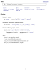
Positive Edge Polarity
vali
d
Negative Edge Polarity
Vcc
Critical
point
Vcc
vali
d
Critical
point
Vdd
Vdd
Figure 1 : Positive and Negative Edge Polarity
There are many design related problems that can cause noisy serial clock lines which can potentially cross the
critical voltage multiple times per one clock pulse. The example below presents two variations of the same
serial clock signal - one has a large signal reflection which causes each period of the serial clock to cross the
critical point multiple times. This will cause the state machine within the serial port to sample the serial data lines
twice per clock period causing the serial data to become corrupted. The other signal is properly compensated
so no reflections occur and the data is sampled once per period.
This signal does not contain reflections
This signal contains reflections
Figure 2: Signals with reflections
The following sections present specific design strategies to avoid problems like this one.
Decoupling the DSP’s Vcc and GND Pins
The DSP should have a .1µF capacitor connected between each of its Vcc and Gnd (Vdd) pins. This helps
keep the power supply to the DSP clean of voltage spikes and dips on the Vcc and Gnd lines. Large spikes
and dips in the Vcc and Gnd lines can cause the processor to jump into an unknown state potentially causing the
processor to crash. These capacitors should be placed as close as possible to the actual Vcc and Gnd pins of
the chip for maximum effectiveness.
Hardware Construction (PCB vs. Wirewrap)
EN-74
Page 2
Technical Notes on using Analog Devices’ DSP components and development tools
Phone: (800) ANALOG-D, FAX: (781) 461-3010, FTP: ftp.analog.com, EMAIL: dsp.support @analog.com