1
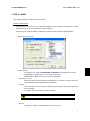
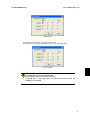
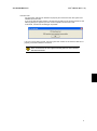
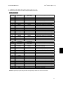
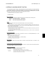
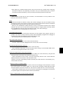
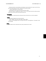
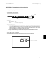
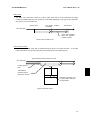
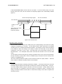
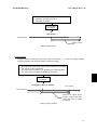
KIT-V850E2/MN4-TP-H
User’s Manual (Rev. 1.01)
RealTimeEvaluator
KIT-V850E2/MN4-TP-H
User’s Manual (Rev. 1.01)
Software Version Up
* The latest RTE for Win32 (Rte4win32) can be down-loaded from following URL.
http://www.midas.co.jp/products/download/english/program/rte4win_32.htm
Notice
* The copyright associated with KIT-V850E2/MN4-TP-H (including software and manual) are proprietary to
Midas Lab. Co., Ltd.
* This software and manual are protected under applicable copyright laws, and may not be copied,
redistributed, or modified in whole or in part, in any way without explicit prior written permission from Midas
Lab. Co., Ltd.
* While this product was manufactured with all possible care, Midas Lab. Co., Ltd. does not guarantee that
this product is free from any problem.
* Midas Lab. Co., Ltd. and its distributor assume no responsibility whatsoever for any result of using this
product.
* The contents and specifications of this software and this manual are subject to change without notice.
Trademarks
* MS-Windows, Windows, MS, and MS-DOS are the trademarks of Microsoft Corporation, U.S.A.
* The names of the programs, systems, CPUs, and other products that appear in this document are usually
trademarks of the manufacturer of the corresponding product.
1
User’s Manual (Rev. 1.01)
KIT-V850E2/MN4-TP-H
REVISION HISTORY
st
Rev.1.00
2010.03.20
PRELIMINARY 1 edition
Rev.1.01
2010.06.24
1 edition
st
2
User’s Manual (Rev. 1.01)
KIT-V850E2/MN4-TP-H
CONTENTS
1. OVERVIEW .............................................................................................................................................. 4
2. HARDWARE SPECIFICATIONS.............................................................................................................. 5
3. RTE FOR WIN32 ...................................................................................................................................... 7
Execution ChkRTE2.exe ........................................................................................................................... 7
4. INITIALIZATION COMMANDS .............................................................................................................. 10
To use Multi............................................................................................................................................. 10
5. INTERFACE SPECIFICATION (PB-NEXUS-N38) ................................................................................. 11
Signal connection list .............................................................................................................................. 11
6. INTERNAL FLASH ROM SUPPORT FUNCTION .................................................................................. 12
Block management ................................................................................................................................. 12
Cache...................................................................................................................................................... 12
Write internal flash ROM ......................................................................................................................... 12
INIT command ........................................................................................................................................ 12
Changing automatic programming (writing) mode .................................................................................. 12
Cache control commands ....................................................................................................................... 12
Notes ....................................................................................................................................................... 13
7. PRECATIONS ........................................................................................................................................ 14
Precautions of operation ......................................................................................................................... 14
Breakpoints ............................................................................................................................................. 14
HALT instruction ..................................................................................................................................... 15
Trace ....................................................................................................................................................... 15
Trace display while execution ................................................................................................................. 15
Stop of trace with a multi-core ................................................................................................................ 15
Internal flash ROM write with a multi-core .............................................................................................. 15
Same time break/execution and synchronous break .............................................................................. 15
INIT command ........................................................................................................................................ 16
Register................................................................................................................................................... 16
Others ..................................................................................................................................................... 16
APPENDIX A. PACKAGE DRAWING OF THE POD SECTION ................................................................ 17
Package drawing of the pod section ....................................................................................................... 17
APPENDIX B. DETAILS OF TRACE FUNCTIONS.................................................................................... 18
Overview of the trace function................................................................................................................. 18
Delay count ............................................................................................................................................. 19
Trace execution mode............................................................................................................................. 19
Sub-switch, section, and qualify .............................................................................................................. 20
Starting trace ........................................................................................................................................... 20
Trigger condition ..................................................................................................................................... 21
Stopping trace ......................................................................................................................................... 22
Terminating trace .................................................................................................................................... 22
Forced delay mode ................................................................................................................................. 23
3
User’s Manual (Rev. 1.01)
KIT-V850E2/MN4-TP-H
1. OVERVIEW
KIT-V850E2/MN4-TP-H is a kit that works in-circuit emulation using NEC RISC microprocessor
V850E2/MN4 family.
This product comes with the following items:
1. RTE for Win32 setup disk
:
1
2. License sheet
:
1
3. User's Manual
:
1
In addition to the above items, the following items are required for using this product.
4. ICE unit
:
RTE-2000H-TP-x-x
5. Pod
:
PB-NEXUS-N38
4
User’s Manual (Rev. 1.01)
KIT-V850E2/MN4-TP-H
2. HARDWARE SPECIFICATIONS
Emulation
Target device
V850E2/MN4
RTE-TP type to be used
RTE-2000H-TP + PB-NEXUS-N38
Emulation functions
Operating frequency
Interface
100KHz - …
Nexus specification
Operation voltage
JTAG-CLK
Internal ROM
3.3V
(A part of signal is converted into 5V by the converter)
10KHz - 25MHz
Automatic write function available
Event function
Number of events
Setting of execution address
8
Setting of data access
6
Setting of DMA cycles
6
Address specification
Conditions Data specification
Status specification
Etc.
Number of sequential unit stages
Path counter
Range specification is possible
Range specification is possible
R, W, R/W
4
12 bits
Break functions
Hardware breakpoints
access breakpoints *6
Address specification
Data specification
Status specification
Software breakpoints
4
Maskable
Maskable
R, W, R/W
100 (Internal flash ROM area is limitation) *5
Event breaks
Supported
Step breaks
Supported
Manual breaks
Supported
External breaks (High/Low edge) *7
Supported
Trace functions
Trace data bus
8bit
Trace memory
1M-words
Trigger setting
Execution address *6
Supported
Data access *6
Supported
Event
Supported
External input
Start/stop specification (sub-switch) *6
Trace delay
Trace clock
Time tag
Supported
Supported
0 - FFFFF
DDR - 133MHz (max)
100ns - 30h
Disassembled trace data display function
Provided
Complete trace mode specification function
(no real time)
Provided
5
User’s Manual (Rev. 1.01)
KIT-V850E2/MN4-TP-H
ROM emulation functions *4
Map function in block (USER/EMEM)
64K-Word
Used as RAM
Supported
Memory capacity
8M - 128M bytes
Access time <(): burst cycle>
35ns (30ns) *1
Operation voltage
1.8V - 5V *2
Electrical condition
LV-TTL, 5V tolerant *3
Number of ROMs that can be emulated
DIP-32pin-ROM (8bit-ROM)
4 (max)
DIP-40/42pin-ROM (16bit-ROM)
4 (max)
Extend STD-16BIT-ROM connector
4 (max)
Sizes of ROMs that can be emulated (bits)
DIP-32-ROM(8-bit bus)
1M,2M,4M,8M(27C010/020/040/080)
DIP-40-ROM(16bit-bus)
1M,2M,4M(27C1024/2048/4096)
DIP-42-ROM(16bit-bus)
8M,16M(27C8000/16000)
Extend STD-16BIT-ROM (16-bit bus)
1M,2M,4M,8M,16M,32M,64M,128M,256M (32M bytes)
Bus width specification (bits)
8/16/32
Pin mask functions
STOP, WAIT-, HLDRQ, RESET-
Execution time measurement function
(the value when the JTAGCLK frequency is 25 MHz is
shown in parentheses.)
Resolution (ns)
t = doubled JTAGCLK frequency (80ns)
Maximum measurement time (ns)
t*2
31
(about 171s)
*1, 2, 3: Values when RTE-2000H-TP + CBL-STD16-2K is used.
*2: Note that the DC characteristics of each cable may not electrically match when the supply voltage is 2.3
V or less.
*4: The user system must have a ROM socket or dedicated connector for connecting the ROM emulation
cable. For details, refer to the manual of the RTE-2000H-TP main unit.
Up to four E.MEM boards can be mounted on the RTE-2000H-TP, and the maximum capacity is 128M
bytes.
*5: The maximum number of the software break point in a internal ROM area is eight points
*6: The following function shares the same resources.
- access breakpoints
- Trace trigger by execution address and data access
- Pass condition of sub-switch
*7: An EVTI signal is occupied when using external signal breaking..
*8: Please consult, when you wish to have working by 100kHz or less.
6
KIT-V850E2/MN4-TP-H
User’s Manual (Rev. 1.01)
3. RTE for WIN32
This chapter describes the setting of RTE for WIN32.
Execution ChkRTE2.exe
After finishing to connect to the user system and apply the power supply for all equipments, execute
ChkRTE2.exe to set up the configuration of "RTE for WIN32".
Please set up the "RTE for WIN32" configuration at least one time for newly installed hardware.
<Setting up RTE-products>
<Selecting RTE>
From Product List, select the V850E2/MN4-TP (XXXXX) located beneath the TP tree.
* V850E2/MN4-TP (Single Core): For one core microprocessor.
* V850E2/MN4-TP (Multi Core): For two cores microprocessor.
<Selecting I/F-1, I/F-2>
Select and specify the host interface that suitable for your system from pull-down menu.
(The example shows that USB Interface is assigned.)
<License>
Click this button to set up license to checking with the license setup sheet attached to
the KIT package.
For details, refer to the manual of “RTE for WIN32”.
rte4win32 should use a version higher than Ver.7.04.06 and it.
<Option>
This button is clicked. And please input the security ID code.
7
User’s Manual (Rev. 1.01)
KIT-V850E2/MN4-TP-H
<Initial status>
The following is the example of an input of the ID code.
When the ID code is changed, please be sure to set up using this option.
<Input example>
Security function for the internal ROM/flash memory To start the debugger,
the 12-byte ID code must be authenticated.
For the details, refer to the manual of the CPU.
●If the ID code on this option does not match the ID code of CPU, the
debugger is not started.
8
KIT-V850E2/MN4-TP-H
User’s Manual (Rev. 1.01)
<Function test>
For the function test RTE for WIN32 must properly be connected to the user system and
identified by the ID code.
If you set up RTE and then perform a function test according to the screen instructions, the
following dialog box appears upon the normal completion of the function test.
In this state, control from the debugger is possible.
If an error occurs during the test, the user system has a failure or the JTAG-IF cable is not
properly connected. Check its connection.
Perform the ChkRTE2.exe function test after the RTE-xxxx-TP has
been connected to the user system and the power to all the devices
has been turned on.
9
KIT-V850E2/MN4-TP-H
User’s Manual (Rev. 1.01)
4. INITIALIZATION COMMANDS
Before debugging can be started, system initialization is required, depending on hardware of the user
system.
The following commands are available for system initialization. Be sure to set up correctly before start to
use the system.
To use Multi
Use the following commands in the target window.
IFROMENV command
- Setup of internal flash ROM writing
ENV command
- Specify pin mask
- Specify JTAG clock
- Others
ROM command
- Specify ROM emulation condition
NC/NCD command
- Specify data cache area for debugger
NSPB/NSPBD command
- Specify forbid software break area
NROM/NROMD command
- Specify forced user area
10
User’s Manual (Rev. 1.01)
KIT-V850E2/MN4-TP-H
5. INTERFACE SPECIFICATION (PB-NEXUS-N38)
Signal connection list
Pin
number
1
3
5
7
9
11
13
15
17
19
21
23
25
27
29
31
33
35
37
Connected
signal name
GND
TCK
TMS
TDI
TDO
MSEO0
MSEO1
OPEN
MCKO
OPEN
MDO[0]
MDO[1]
MDO[2]
MDO[3]
MDO[4]
MDO[5]
MDO[6]
MDO[7]
GND
Input/Output
(User Side)
--Input
Input
Input
Output
Output
Output
--Output
--Output
Output
Output
Output
Output
Output
Output
Output
---
Pin
number
2
Connected
signal name
GND
Input/Output
(User Side)
---
4
VCCIO
Output
6
8
10
12
14
16
18
20
22
24
26
28
30
32
34
36
38
TRSTRESETFLMD0
RDYZ(RDY-)
EVTO
EVTI
OPEN
OPEN
----------------GND
Input
BIDIR
Input
Output
Output
Input
----Output
Output
Output
Output
Output
Output
Output
Output
---
Treatment (User Side)
Connection to the GND
4.7K - 10KΩ pullup or pulldown
4.7K - 10KΩ pullup or pulldown
4.7K - 10KΩ pullup or pulldown
22 - 33Ω series resistor (recommended)
10- 22Ω series resistor (recommended)
10- 22Ω series resistor (recommended)
10- 22Ω series resistor (recommended)
10- 22Ω series resistor (recommended)
10- 22Ω series resistor (recommended)
10- 22Ω series resistor (recommended)
10- 22Ω series resistor (recommended)
10- 22Ω series resistor (recommended)
10- 22Ω series resistor (recommended)
10- 22Ω series resistor (recommended)
10- 22Ω series resistor (recommended)
Connection to the GND
Treatment (User Side)
Connection to the GND
Connection to the power supply (+3.3V)
* For power monitoring
4.7K - 50KΩ pulldown
Impress RESET (O.C.) … option
4.7K - 50KΩ pulldown
22 - 33Ω series resistor (recommended)
22 - 33Ω series resistor (recommended)
4.7K - 50KΩ pullup
Connection to the GND(recommended)
Connection to the GND(recommended)
Connection to the GND(recommended)
Connection to the GND(recommended)
Connection to the GND(recommended)
Connection to the GND(recommended)
Connection to the GND(recommended)
Connection to the GND(recommended)
Connection to the GND
Remark: Input/Output (user side) indicates the input/output direction at the user board side.
11
User’s Manual (Rev. 1.01)
KIT-V850E2/MN4-TP-H
6. INTERNAL FLASH ROM SUPPORT FUNCTION
This kit supports automatic writing to internal flash ROM. When write operation to the Flash ROM area
from debugger (download or memory write) happens, the change will be saved (cache) in the Host
machine. Then, when the program execution command is issued, if there are different portion on the flash
ROM, flash is automatically written with that saved change before execution.
To disable this function, use ”ifromenv” command.
The detail is below.
Block management
Internal flash ROM is divided into 4KB block. Each block is classified into the following state.
INVALID : Not cached (not saved)
<initial state>
VALID
: Cache and Internal flash ROM is the same
DIRTY
: Cache and internal flash ROM is different
Cache
Write data and the contents of the internal flash ROM are cached at the cases below.
- Memory read
When the block of a cache is INVALID, the data of internal flash ROM are read and it puts into a
cache. The state of that area becomes VALID. When read internal flash ROM area and if that block is
VALID or DIRTY, use cached data.
- Memory write (download and other write operation)
When the block of a cache is INVALID, the data of internal flash ROM are read and it puts into a
cache. Writing data are put into a cache.
A state is set to DIRTY when writing data differ from the data of a cache. It is set to VALID when
data are the same.
Write internal flash ROM
The writing to an internal flash ROM is performed at the time of execution(RUN,STEP) of a user
program.
- Before execution, DIRTY block is written.
- Step of writing to internal flash ROM
ERASE -> WRIT E->internal VERIFY (-> READ VERIFY).
- After writing, the state is set to VALID.
INIT command
INIT command makes all the blocks states to INVALID. Internal flash ROM is not written by this
command.
Changing automatic programming (writing) mode
When you change automatic programming mode by “ifromenv” command, all the cache will be INVALID.
Internal flash ROM is not written by this change.
Cache control commands
There are a few commands to change cache states directly.
- ifromclear
: Set all the cache to INVALID.
Internal flash ROM is not written by this command.
- ifromflush
: The cache data of DIRTY are written in an internal flash ROM.
The state of the block is set to VALID.
12
User’s Manual (Rev. 1.01)
KIT-V850E2/MN4-TP-H
- ifromrefill
: The data of all internal flash ROMs are read and it puts into a cache.
All the states are set to VALID.
Notes
- When the state of a cache is DIRTY, the writing to an internal flash ROM is done at the time of program
execution. Program execution is kept waiting until the writing to an internal flash ROM finishes. Writing
time is about 20 seconds.
- The MULTI (debugger) may show below messages in this case.
In that case, click Continue.
To increase time out limit, use below setting for MULTI.
SERVERTIMEOUT=30
13
KIT-V850E2/MN4-TP-H
User’s Manual (Rev. 1.01)
7. PRECATIONS
This chapter provides the precautions you should observe when using KIT-V850E2/MN4-TP-H.
Precautions of operation
1) Do not turn on the power to the user system while the power to ICE unit is off. This operation
causes trouble of both sides.
2) ICE unit externally controls the debugging control unit (DCU) built into the CPU.
ICE unit does not operate correctly unless the following conditions are satisfied:
* ICE unit is properly connected to the user system using the JTAG-IF cable.
* The power to the user system is on so that the CPU can run correctly.
* The correct ID code is set. (Refer to Chapter 3, "RTE for WIN32".)
3) When multi core CPU is debugged by using Multi of the GHS Co., the method of starting the server
is as follows:
connect rteserv2 -cpu PE1 -cpu PE2 -multicore
Please do not start the microcomputer of a dual core only by PE1 as follows.
connect rteserv2 -cpu PE1 -multicore <- NG
4) When you start on the microcomputer of a single core, please start rteserv2 without a parameter.
MULTI degugger should use a version higher than Ver 5.1.6c and it.
Breakpoints
- The maximum number of the break point which can be set to a ROM area is eight points by an
EXTBRK function. These eight points are treated as a software break point.
- The break point (eight points) for which the break point set to a ROM area from on the sauce window
of a MULTI debugger used the EXTBRK function is used.
When using MULTI
MULTI implicitly uses breakpoints in the following cases:
1. When Step, Next, Return Come, and others are executed at the
source level: 2 points
2. When the execution is started immediately after downloding at the
source level: 1 point
3. When the syscall function is used: 1 point (always)
To debug a program stored in internal flash ROM, take some measures so
that the maximum number of set breakpoint is not also exceeded when
the above points are included. if he maximum number is exceeded, the
following error message appears:
(0x87) Exhaust the number of settings
- As for a setup of the break point to a RAM area, a software break point (rewriting to a break
instruction) is used.
With a dual core microcomputer, even if this software break point is a break point set up from which
core, if that address is executed, it will take a break.
However, since ICE performs continuation execution automatically when it takes a break with cores
other than the set-up core, a debugger does not show having taken a break seemingly.
14
KIT-V850E2/MN4-TP-H
User’s Manual (Rev. 1.01)
- When setting up a software break point with a dual core and the core of another side is executing,
ICE takes a break the core temporarily, and after it sets up a software break point, it performs
processing resumed immediately. (It is the processing automatically performed inside ICE) .
.
HALT instruction
When a break is made with the HALT instruction, the break address is the top address of the
instruction next to the HALT instruction.
Trace
There are two kinds of methods of tracing with a MULTI debugger. They are the method of using
TimeMachine of Multi, and a method of using the trace command of the internal command of rte4win32
in a target window. These functions cannot be used at the same time.
When you use TimeMachine of Multi, please do not use a trace-related command with an internal
command. And, when you use trace with an internal command in a target window conversely, please
set up TimeMachine invalid, and when initial setting remains, use it after re-setting up.
* TimeMachine has not corresponded as of June 14, 2010.
Trace display while execution
If it is the program of an internal flash ROM area, the trace display under program execution is
possible. This is done by saving to Host PC (cache), when downloading a program from a debugger to
an internal flash ROM. If the debugger supports this method it works.
Set caching by internal command (“ifromenv” command).
Stop of trace with a multi-core
If trace is stopped by one of cores, trace of all cores will stop.
Moreover, if the trace result is displayed as one of cores, trace of all cores will stop.
Internal flash ROM write with a multi-core
When writing in an internal flash ROM, both of cores must stop.
Also in automatic writing, both of cores must stop. And the writing to an internal flash ROM is done
at the time of the program execution of one of cores.
Same time break/execution and synchronous break
The break and the execute can be controlled to the Multi core at the same time by using the task
manager of MULTI. But there is time difference between cores.
When a "autobreak" function is used, it can stop synchronously with both cores. There is little time
difference between cores for this to use the function of ICE.
However, in the case of all breaking conditions (a break point, STEP execution, forced breaking, etc.),
note that other cores stop.
Sequence access of a specific register
Although ICE enables the function in which access from the debugger under break does not block
the access sequence of a specific register, it is a time of both cores taking a break that this function
becomes effective in the case of a dual core. This function is invalid while one of cores are executing.
When it takes a break and only core of one of the two is operated from a debugger in the sequence
of a specific register, the sequence under access may be blocked.. .
A timer, a serial interface, an A/D converter under break
15
KIT-V850E2/MN4-TP-H
User’s Manual (Rev. 1.01)
ICE has the function to stop working of the following circuits at the time of a break, and can set it up
with the svstop parameter of the env command of an internal command.
A timer, serial interface, an A/D converter.
A default setting is OFF. Please set up this parameter if needed.
When this function is enabled with a dual core, if one of cores take a break, that working will stop.
Cautions are necessary when executing asynchronously.
INIT command
When “INIT” command (internal command) is used for the multi core, all cores are initialized.
Register
The following registers cannot change the value.
DBPC, DBPSW, DIR, BPAV, BPAM, BPDV, BPDM, DBWR
There are some debuggers which can change them. But it is only appearance. The register of CPU
is not changed.
Others
- When release notes are attached to the product, please be sure to read it.
16
User’s Manual (Rev. 1.01)
KIT-V850E2/MN4-TP-H
APPENDIX A. Package drawing of the pod section
Package drawing of the pod section is shown below.
Package drawing of the pod section
Flex PCB
51.000mm
Bottom Cover
<Connector>
Manufacturer: AMP
Model:
2-767004-2 (receptacle)
<Wiring and wiring length>
• Trace-related signals change at very high speeds. Wiring lines should be the same and short as
much as possible (length of 50 mm or less is recommended) with 50-Ω characteristic impedance.
Apply processing such as shielding so that the trace signals are not affected each other and the
signals are not affected by crosstalks from other circuit signals.
• Mount a series resistance for a series match near the CPU for output signals from the CPU.
• In principle, connect all signals to ICE connectors only.
<Layout of the connector on the board>
The figure below shows an example of the physical layout of the connector on the board.
CPU
MICTOR connector
1
37
2
ICE connection direction
38
17
User’s Manual (Rev. 1.01)
KIT-V850E2/MN4-TP-H
Appendix B. Details of Trace functions
This appendix describes the real-time trace function.
Overview of the trace function
The real-time trace function writes the details of the execution (trace data) output from the CPU in the
trace buffer in the ICE for each execution. You can check the data using the trace command.
You can set the trace mode, trace start condition, trigger condition, section condition, qualify condition,
and other conditions to specify the loading of trace data. For the flow of loading trace data, see Figures
1 and 2.
The trigger condition
is satisfied
Start of trace
End of trace
CPU execution
Data loaded into the ICE
CPU
Trace data
Trace
Figure 1 Flow of loading trace data
End point
Trigger point
If the trace buffer in
the ICE becomes
full, it is overwritten
from the beginning
Start point
Figure 2 Trace data in the ICE
18
User’s Manual (Rev. 1.01)
KIT-V850E2/MN4-TP-H
Delay count
The delay count means the number of cycles in which trace data is to be loaded after the trigger
condition is satisfied (Figure 3). The number of cycles differs depending on the type of CPU execution.
One cycle is not one execution unit.
Start of trace
The trigger condition
is satisfied
End of trace
CPU execution
Trace data is loaded
during the specified
number of cycles
Figure 3 Flow of delay count
Trace execution mode
In the real-time mode, trace data is loaded with priority given to the CPU execution.
If the trace
buffer (FIFO) in the CPU becomes full, part of trace data may not be loaded (Figure 4).
When the trace buffer in the CPU is full
CPU execution
Loading of trace
data
The details of
execution during
this section are lost
Overflow information and
not trace data is written in
the trace buffer
Figure 4 Real-time mode
19
User’s Manual (Rev. 1.01)
KIT-V850E2/MN4-TP-H
In the non-real-time mode, all trace data can be loaded.
If the trace buffer (FIFO) in the CPU
becomes full in this mode, the CPU execution is temporarily stopped and is automatically restarted
(Figure 5).
The CPU is temporarily stopped
The CPU is restarted
CPU execution
Loading of trace
data
Trace data is not loaded
when the CPU is
temporarily stopped
Figure 5 Non-real-time mode
Sub-switch, section, and qualify
The sub-switch indicates whether OR or AND (set by tenv [subor|suband]) of the section and qualify
conditions are satisfied (on) or not (off).
You can specify cycles in which trace data is to be loaded
according to the on or off status (sswon/sswoff command).
By specifying cycles in which trace data is
to be loaded for sswon and nothing to be loaded for sswoff, the on/off status of this sub-switch
corresponds to the start or stop of trace.
described above.
(The initial value of the sswon/sswoff command is as
In the description below, these commands are assumed to be set to their initial
value.)
You can specify a section using the tsp1 and tsp2 commands and evt secon and secoff parameters.
Use tsp1 and secon to specify that a section is established (on) and tsp2 and secoff to specify that a
section is not established (off).
The event condition specified for qualify in the evt command is used as a qualify condition.
When the
event condition is satisfied, the qualify condition is also satisfied.
Starting trace
To start loading trace data, the following methods are available:
Forced start method (tron force) and
the method using the status of the sub-switch according to the section and qualify setting.
To set the loading condition using the sub-switch, use sswon and sswoff.
(Figure 6)
Usually, specify cycles in
which trace data is to be loaded for sswon and nothing to be loaded for sswoff.
According to this
setting, trace data is loaded in the sub-switch on state and the loading of trace data is stopped in the
sub-switch off state.
20
User’s Manual (Rev. 1.01)
KIT-V850E2/MN4-TP-H
• Start unconditionally loading trace data (tron force)
• Set section point (tsp, evt secon)
• Set qualify (evt qualify)
The condition
is satisfied
Start of trace
CPU execution
Loading of trace
data
Figure 6 Starting trace
Trigger condition
A trigger condition is used as the start point of delay count (Figure 7).
You can set a trigger condition
to check the details of the execution before and after the trigger.
• The instruction at the trigger address (tp) is executed or trace data
(td1, td2, td3, or td4) is accessed.
• The external signal condition is as specified (tron noext|posi|nega).
• The event match point factor is established (evt match).
The condition
is satisfied
The trigger condition is satisfied
End of trace
CPU execution
Execution is traced during
as many cycles as the delay
count and trace is forcibly
terminated.
Figure 7 Trigger condition
21
User’s Manual (Rev. 1.01)
KIT-V850E2/MN4-TP-H
Stopping trace
To stop loading trace data, use the status of the sub-switch according to the section and qualify
setting.
(Figure 8)
To set the loading condition using the sub-switch, use sswon and sswoff.
Usually, specify cycles in
which trace data is to be loaded for sswon and nothing to be loaded for sswoff.
According to this
setting, trace data is loaded in the sub-switch on state and the loading of trace data is stopped in the
sub-switch off state.
• Set section point (tsp2, evt secoff)
• Set qualify (evt qualify)
The condition
is satisfied
Stop of trace
Start of trace
Stop of trace
CPU execution
Loading of trace
data
Loading of trace
data
Figure 8 Stopping trace
Terminating trace
After trace is terminated, no more trace data is loaded.
When the end condition is satisfied, unlike the stop condition, trace is not restarted (Figure 9).
• Stop CPU execution
• Forcibly terminate trace (troff)
• End delay count
The condition
is satisfied
Start of trace
End of trace
CPU execution
No more data is loaded
Loading of trace
data
Figure 9 Terminating trace
22
User’s Manual (Rev. 1.01)
KIT-V850E2/MN4-TP-H
Forced delay mode
In the forced delay mode, trace is forcibly terminated when trace data is loaded during the specified
delay count (number of cycles) after the start of trace.
In this mode, the trigger condition is ignored
(Figure 10).
When CPU execution starts, trace is started in this mode.
Start of trace
End of trace
CPU execution
Trace terminates after trace
data is loaded during as many
cycles as the delay count.
Figure 10 Forced delay mode
23