1
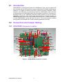
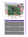
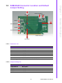
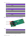
User Manual SOM-DB5800 Development Board for COM Express Type 6 Pin-out Modules Copyright The documentation and the software included with this product are copyrighted 2011 by Advantech Co., Ltd. All rights are reserved. Advantech Co., Ltd. reserves the right to make improvements in the products described in this manual at any time without notice. No part of this manual may be reproduced, copied, translated or transmitted in any form or by any means without the prior written permission of Advantech Co., Ltd. Information provided in this manual is intended to be accurate and reliable. However, Advantech Co., Ltd. assumes no responsibility for its use, nor for any infringements of the rights of third parties, which may result from its use. Acknowledgements Intel and Pentium are trademarks of Intel Corporation. Microsoft Windows and MS-DOS are registered trademarks of Microsoft Corp. All other product names or trademarks are properties of their respective owners. Product Warranty (2 years) Advantech warrants to you, the original purchaser, that each of its products will be free from defects in materials and workmanship for two years from the date of purchase. This warranty does not apply to any products which have been repaired or altered by persons other than repair personnel authorized by Advantech, or which have been subject to misuse, abuse, accident or improper installation. Advantech assumes no liability under the terms of this warranty as a consequence of such events. Because of Advantech’s high quality-control standards and rigorous testing, most of our customers never need to use our repair service. If an Advantech product is defective, it will be repaired or replaced at no charge during the warranty period. For outof-warranty repairs, you will be billed according to the cost of replacement materials, service time and freight. Please consult your dealer for more details. If you think you have a defective product, follow these steps: 1. Collect all the information about the problem encountered. (For example, CPU speed, Advantech products used, other hardware and software used, etc.) Note anything abnormal and list any onscreen messages you get when the problem occurs. 2. Call your dealer and describe the problem. Please have your manual, product, and any helpful information readily available. 3. If your product is diagnosed as defective, obtain an RMA (return merchandize authorization) number from your dealer. This allows us to process your return more quickly. 4. Carefully pack the defective product, a fully-completed Repair and Replacement Order Card and a photocopy proof of purchase date (such as your sales receipt) in a shippable container. A product returned without proof of the purchase date is not eligible for warranty service. 5. Write the RMA number visibly on the outside of the package and ship it prepaid to your dealer. SOM-DB5800 User Manual Part No. 2006580000 Edition 1 Printed in Taiwan July 2011 ii Declaration of Conformity CE This product has passed the CE test for environmental specifications when shielded cables are used for external wiring. We recommend the use of shielded cables. This kind of cable is available from Advantech. Please contact your local supplier for ordering information. CE This product has passed the CE test for environmental specifications. Test conditions for passing included the equipment being operated within an industrial enclosure. In order to protect the product from being damaged by ESD (Electrostatic Discharge) and EMI leakage, we strongly recommend the use of CE-compliant industrial enclosure products. FCC Class A Note: This equipment has been tested and found to comply with the limits for a Class A digital device, pursuant to part 15 of the FCC Rules. These limits are designed to provide reasonable protection against harmful interference when the equipment is operated in a commercial environment. This equipment generates, uses, and can radiate radio frequency energy and, if not installed and used in accordance with the instruction manual, may cause harmful interference to radio communications. Operation of this equipment in a residential area is likely to cause harmful interference in which case the user will be required to correct the interference at his own expense. FCC Class B Note: This equipment has been tested and found to comply with the limits for a Class B digital device, pursuant to part 15 of the FCC Rules. These limits are designed to provide reasonable protection against harmful interference in a residential installation. This equipment generates, uses and can radiate radio frequency energy and, if not installed and used in accordance with the instructions, may cause harmful interference to radio communications. However, there is no guarantee that interference will not occur in a particular installation. If this equipment does cause harmful interference to radio or television reception, which can be determined by turning the equipment off and on, the user is encouraged to try to correct the interference by one or more of the following measures: Reorient or relocate the receiving antenna. Increase the separation between the equipment and receiver. Connect the equipment into an outlet on a circuit different from that to which the receiver is connected. Consult the dealer or an experienced radio/TV technician for help. iii SOM-DB5800 User Manual Technical Support and Assistance 1. 2. Visit the Advantech website at http://support.advantech.com where you can find the latest information about the product. Contact your distributor, sales representative, or Advantech's customer service center for technical support if you need additional assistance. Please have the following information ready before you call: – Product name and serial number – Description of your peripheral attachments – Description of your software (operating system, version, application software, etc.) – A complete description of the problem – The exact wording of any error messages Warnings, Cautions and Notes Warning! Warnings indicate conditions, which if not observed, can cause personal injury! Caution! Cautions are included to help you avoid damaging hardware or losing data. e.g. There is a danger of a new battery exploding if it is incorrectly installed. Do not attempt to recharge, force open, or heat the battery. Replace the battery only with the same or equivalent type recommended by the manufacturer. Discard used batteries according to the manufacturer's instructions. Note! Notes provide optional additional information. Document Feedback To assist us in making improvements to this manual, we would welcome comments and constructive criticism. Please send all such - in writing to: [email protected] Packing List Before setting up the system, check that the items listed below are included and in good condition. If any item does not accord with the table, please contact your dealer immediately. 1 SOM-DB5800-00A1E 1 SOM-EA20 (9696EA2000E) HDMI/DP Riser Card 1 Serial ATA Cable 7P/7P 30 cm 1 Flat COM Port Cable 1 I/O Shield Bracket SOM-DB5800 User Manual iv Safety Instructions 1. 2. 3. Read these safety instructions carefully. Keep this User Manual for later reference. Disconnect this equipment from any AC outlet before cleaning. Use a damp cloth. Do not use liquid or spray detergents for cleaning. 4. For plug-in equipment, the power outlet socket must be located near the equipment and must be easily accessible. 5. Keep this equipment away from humidity. 6. Put this equipment on a reliable surface during installation. Dropping it or letting it fall may cause damage. 7. The openings on the enclosure are for air convection. Protect the equipment from overheating. DO NOT COVER THE OPENINGS. 8. Make sure the voltage of the power source is correct before connecting the equipment to the power outlet. 9. Position the power cord so that people cannot step on it. Do not place anything over the power cord. 10. All cautions and warnings on the equipment should be noted. 11. If the equipment is not used for a long time, disconnect it from the power source to avoid damage by transient overvoltage. 12. Never pour any liquid into an opening. This may cause fire or electrical shock. 13. Never open the equipment. For safety reasons, the equipment should be opened only by qualified service personnel. 14. If one of the following situations arises, get the equipment checked by service personnel: The power cord or plug is damaged. Liquid has penetrated into the equipment. The equipment has been exposed to moisture. The equipment does not work well, or you cannot get it to work according to the user's manual. The equipment has been dropped and damaged. The equipment has obvious signs of breakage. 15. DO NOT LEAVE THIS EQUIPMENT IN AN ENVIRONMENT WHERE THE STORAGE TEMPERATURE MAY GO BELOW -20° C (-4° F) OR ABOVE 60° C (140° F). THIS COULD DAMAGE THE EQUIPMENT. THE EQUIPMENT SHOULD BE IN A CONTROLLED ENVIRONMENT. 16. CAUTION: DANGER OF EXPLOSION IF BATTERY IS INCORRECTLY REPLACED. REPLACE ONLY WITH THE SAME OR EQUIVALENT TYPE RECOMMENDED BY THE MANUFACTURER, DISCARD USED BATTERIES ACCORDING TO THE MANUFACTURER'S INSTRUCTIONS. The sound pressure level at the operator's position according to IEC 704-1:1982 is no more than 70 dB (A). DISCLAIMER: This set of instructions is given according to IEC 704-1. Advantech disclaims all responsibility for the accuracy of any statements contained herein. v SOM-DB5800 User Manual Safety Precaution - Static Electricity Follow these simple precautions to protect yourself from harm and the products from damage. To avoid electrical shock, always disconnect the power from your PC chassis before you work on it. Don't touch any components on the CPU card or other cards while the PC is on. Disconnect power before making any configuration changes. The sudden rush of power as you connect a jumper or install a card may damage sensitive electronic components. SOM-DB5800 User Manual vi Contents Chapter 1 General Information ............................1 1.1 1.2 Introduction ............................................................................................... 2 Connectors and Jumper Setting................................................................ 2 1.2.1 SOM-DB5800 Connector Location ............................................... 2 Figure 1.1 SOM-DB5800 Connector Location ............................. 2 1.2.2 SOM-DB5800 Default Jumper Setting .......................................... 3 Figure 1.2 SOM-DB5800 Default Jumper Setting........................ 3 Table 1.1: Connector List ............................................................ 3 Table 1.2: Jumper and Switch Setting List .................................. 4 Table 1.3: DDI1 Digital Display Interface Connector .................. 5 Table 1.4: GPIO1 GPIO Connector ............................................ 8 Table 1.5: LPC_PH1 LPC Pin Header........................................ 9 Table 1.6: LVDS1 LVDS Connector ........................................... 9 Table 1.7: LVDS_INVERTER1 LVDS Inverter Wafer Box....... 10 Table 1.8: DCIN1 Wide Range DCIN Connector..................... 10 Table 1.9: COM3 COM3 Connector ........................................ 10 Table 1.10: COM4 COM4 Connector ........................................ 11 Table 1.11: SYS_FAN1 System FAN Connector ...................... 11 Table 1.12: SMART_FAN1 Smart FAN Connector ................... 11 Table 1.13: SMB1 SMB Wafer Box ........................................... 11 Table 1.14: I2C1 I2C Wafer Box................................................ 11 Table 1.15: SIR1 SIR Wafer Box............................................... 12 Table 1.16: COM2 COM2 Connector ........................................ 12 Table 1.17: GPIO_SDIO_SLT1 GPIO/SDIO select Pin Header 12 Table 1.18: TPM_PP_SLT1 TPM Enable/Disable Pin Header.. 12 Table 1.20: LVDS_VDD_SLT2 LVDS VDD Voltage select Pin Header...................................................................... 13 Table 1.21: DCIN_12V_SLT1 DCIN/12V Voltage select Pin Header .............................................................................. 13 Table 1.22: PSON1 ATX/AT mode select Pin Header .............. 13 Table 1.23: JFP1 Front panel Pin Header ................................. 13 Table 1.24: USB_CLIENT1 USB client/ USB port select Pin Header .............................................................................. 13 Table 1.19: LVDS_INVERTER_SLT1 LVDS inverter voltage select Pin Header ......................................................... 13 Table 1.25: RTC1 Normal operation/Clear COMS select Pin Header...................................................................... 14 Table 1.26: COM2_SET1 RS232/RS422/RS485 select Pin Header .............................................................................. 14 Table 1.27: DDI_DDC_1 Digital Display Interface AUX/DDC Switch ....................................................................... 14 Table 1.28: SW1 LPC Switch SW2 LPC Switch .............................. 14 SOM-EA20 Connector Location and Default Jumper Setting ................. 15 Table 1.29: Connector List .......................................................... 15 Table 1.30: Jumper Setting List................................................... 15 Table 1.31: DDI1_HPD1 Display Port B/HDMI Port B HPD select Pin Header................................................................ 16 Table 1.32: DDI2_HPD1 Display Port C/HDMI Port C HPD select Pin Header................................................................ 16 Table 1.33: DDI3_HPD1 Display Port D/HDMI Port D HPD select Pin Header................................................................ 16 AIMB-4301 Connector Location (Optional) ............................................. 16 Table 1.34: Connector List .......................................................... 16 1.3 1.4 vii SOM-DB5800 User Manual SOM-DB5800 User Manual viii Chapter 1 1 General Information 1.1 Introduction SOM-DB5800 is a development board for COM-Express Type 6 pin-out module that fully complies with the PCI Industrial Computer Manufacture’s PICMG COM Express standard. It is suitable for different form factor modules including COM-Basic, COMCompact, and COM-Ultra. All functions provided by COM-Express type 6 pin-outs are implemented on SOM-DB5800 with the most popular interfaces or connectors for developers ease of use. Additional accessories help customers to do more diverse application evaluations, such as DDI card that provides an extended function on HDMI/Displayport, a PCIe riser card extends PCIe x4 to PCIe x1, and a middle board to make SOM-DB5800 comply with type 10 pin-out. This board provides a reliable testing platform and flexibility for vertical marketing application pre-study. 1.2 Connectors and Jumper Setting 1.2.1 SOM-DB5800 Connector Location SATA1/2 SATA3/4 SPDIF1 PCIE-4x1 USB3_01 LAN1_USB01 COM1 Audio1 VGA1 LPT1 KB1 SIR1 COM2 PCIE-1x1 SDIO1 GPIO1 PCIE-16x1 MiniPCIE1 USB3 2 SMB1 I2C1 USB3 3 DDI1 USB23 USB7 SPI BIOS1 SYS FAN1 SMART FAN1 COM4 CN1 FWH1 EPCard2 LVDS1 LPC_PH1 COM3 EPCard1 ATX1 LVDS INVERTER1 Figure 1.1 SOM-DB5800 Connector Location SOM-DB5800 User Manual 2 SMB_ALT#1 BATLOW#1 PM_WAKE#1 Chapter 1 1.2.2 SOM-DB5800 Default Jumper Setting EXT_THRM#1 SW2 GPIO SDIO SLT1 SW1 RTC1 USB TPM_PP_SLT1 DDI_DDC_1 BIOS_DIS#0 LID_BTN1 PWR_BTN1 SLEEP_BTN1 RST_BTN1 BIOS_DIS#1 PSON1 LVDS_INVERTER_SLT1 JFP1 LVDS VDD SLT2 DCIN 12V SLT1 Figure 1.2 SOM-DB5800 Default Jumper Setting 1.2.2.1 Connector List Table 1.1: Connector List Connector Description CN1* COM Express Connector KB1* PS/2 KB and MS Connector LPT1* Print port Connector COM1* COM Connector VGA1* CRT Connector LAN1_USB01* LAN1, USB0 and USB1 Connector USB3_01* USB3.0 Port0 and Port1 Connector Audio1* Line-in, Line-out and MIC Connector SATA1* SATA1 Connector SATA2* SATA2 Connector SATA3* SATA3 Connector SATA4* SATA4 Connector SPDIF1* SPDIF Connector PCIE-16X1* PCIEx16 Connector DDI1 Digital Display Interface Connector PCIE-4X1* PCIEx4 Connector PCIE-1X1* PCIEx1 Connector SDIO1* SDIO Connector GPIO1 GPIO Pin Header 3 SOM-DB5800 User Manual General Information COM2_SET1 Table 1.1: Connector List FWH1* FWH Connector LPC_PH1 LPC Pin Header MiniPCIE1* MiniPCIE Connector * Items use general interface and not described in this document. 1.2.2.2 Jumper and Switch Setting List Table 1.2: Jumper and Switch Setting List Jumper /Switch Description GPIO_SDIO_SLT1 GPIO/SDIO select Pin Header TPM_PP_SLT1 TPM Enable/Disable Pin Header BIOS_DIS#0 BIOS select Pin Header BIOS_DIS#1 BIOS select Pin Header LVDS_INVERTER_SLT1 LVDS inverter voltage select Pin Header LVDS_VDD_SLT2 LVDS VDD Voltage select Pin Header DCIN_12V_SLT1 DCIN/12V Voltage select Pin Header PSON1 ATX/AT mode select Pin Header JFP1 Front panel Pin Header USB_CLIENT1 USB client/ USB port select Pin Header RTC1 Normal operation/Clear COMS select Pin Header COM2_SET1 RS232/RS422/RS485 select Pin Header DDI_DDC_1 Digital Display Interface AUX/DDC Switch SW1 LPC Switch SW2 LPC Switch PM_WAKE#1 WAKE Button SMB_ALT#1 SMB Alert Button BATLOW#1 Battery Low Button EXT_THRM#1 External Thermal Button RST_BTN1 Reset Button SMB_ALT#1 SMB Alert Button SLEEP_BTN1 Sleep Button PWR_BTN1 Power Button LID_BTN1 LID Button SOM-DB5800 User Manual 4 Table 1.3: DDI1 Digital Display Interface Connector Pin Pin name A1 NC A2 +V12 +V12 A4 GND A5 NC A6 NC A7 NC A8 NC A9 +V3.3 A10 +V3.3 A11 PLTRST# A12 GND A13 NC A14 NC A15 GND A16 DDI1_PAIR5+ A17 DDI1_PAIR5- A18 GND General Information A3 Chapter 1 1.2.2.3 Connector Pin Name Definition A19 NC A20 GND A21 DDI1_PAIR4+ A22 DDI1_PAIR4- A23 GND A24 GND A25 DDI1_PAIR6+ A26 DDI1_PAIR6- A27 GND A28 GND A29 DDI1_HPD A30 NC A31 GND A32 NC A33 NC A34 GND A35 DDI1_CTRLCLK_AUX+ A36 DDI1_CTRLCLK_AUX- A37 GND A38 GND A39 NC A40 NC A41 GND A42 GND A43 DDI2_CTRLCLK_AUX+ A44 DDI2_CTRLCLK_AUX- 5 SOM-DB5800 User Manual Table 1.3: DDI1 Digital Display Interface Connector A45 GND A46 GND A47 DDI2_HPD A48 NC A49 GND A50 NC A51 GND A52 NC A53 NC A54 GND A55 GND A56 NC A57 NC A58 GND A59 GND A60 DDI3_CTRLCLK_AUX+ A61 DDI3_CTRLCLK_AUX- A62 GND A63 GND A64 DDI3_HPD A65 NC A66 GND A67 GND A68 NC A69 NC A70 GND A71 GND A72 NC A73 NC A74 GND A75 GND A76 NC A77 NC A78 GND A79 GND A80 NC A81 NC A82 GND B1 +V12 B2 +V12 B3 +V12 B4 GND B5 NC B6 NC B7 GND B8 +V3.3 B9 NC SOM-DB5800 User Manual 6 +V3.3_DUAL B11 NC B12 NC B13 GND B14 DDI1_PAIR0+ B15 DDI1_PAIR0- B16 GND B17 NC B18 GND B19 DDI1_PAIR1+ B20 DDI1_PAIR1- B21 GND B22 GND B23 DDI1_PAIR2+ B24 DDI1_PAIR2- B25 GND B26 GND B27 DDI1_PAIR3+ B28 DDI1_PAIR3- B29 GND B30 NC B31 NC B32 GND B33 DDI2_PAIR0+ B34 DDI2_PAIR0- B35 GND B36 GND B37 DDI2_PAIR1+ B38 DDI2_PAIR1- B39 GND B40 GND B41 DDI2_PAIR2+ B42 DDI2_PAIR2- B43 GND B44 GND B45 DDI2_PAIR3+ B46 DDI2_PAIR3- B47 GND B48 NC B49 GND B50 DDI3_PAIR0+ B51 DDI3_PAIR0- B52 GND B53 GND B54 DDI3_PAIR1+ B55 DDI3_PAIR1- B56 GND General Information B10 Chapter 1 Table 1.3: DDI1 Digital Display Interface Connector 7 SOM-DB5800 User Manual Table 1.3: DDI1 Digital Display Interface Connector B57 GND B58 DDI3_PAIR2+ B59 DDI3_PAIR2- B60 GND B61 GND B62 DDI3_PAIR3+ B63 DDI3_PAIR3- B64 GND B65 GND B66 NC B67 NC B68 GND B69 GND B70 NC B71 NC B72 GND B73 GND B74 NC B75 NC B76 GND B77 GND B78 NC B79 NC B80 GND B81 NC B82 NC Table 1.4: GPIO1 GPIO Connector Pin Pin name 1 GPI0 2 GPO0 3 GPI1 4 GPO1 5 GPI2 6 GPO2 7 GPI3 8 GPO3 9 GND 10 GND SOM-DB5800 User Manual 8 Chapter 1 Table 1.5: LPC_PH1 LPC Pin Header Pin name 1 CLK33M_PH 2 LPC_AD1 3 PLTRST# 4 LPC_AD0 5 LPC_FRAME# 6 +V3.3 7 LPC_AD3 8 GND 9 LPC_AD2 10 Pull-up via 10K ohm to +V3.3 11 SERIRQ 12 PLTRST# 13 +V5_DUAL 14 +V5 General Information Pin Table 1.6: LVDS1 LVDS Connector Pin Pin name 1 +V3.3_LVDS_PANEL 2 +V3.3_LVDS_PANEL 3 GND 4 GND 5 +V3.3_LVDS_PANEL 6 +V3.3_LVDS_PANEL 7 LVDS0_Z_D0- 8 LVDS1_Z_D0- 9 LVDS0_Z_D0+ 10 LVDS1_Z_D0+ 11 GND 12 GND 13 LVDS0_Z_D1- 14 LVDS1_Z_D1- 15 LVDS0_Z_D1+ 16 LVDS1_Z_D1+ 17 GND 18 GND 19 LVDS0_Z_D2- 20 LVDS1_Z_D2- 21 LVDS0_Z_D2+ 22 LVDS1_Z_D2+ 23 GND 24 GND 25 LVDS0_Z_CLK- 26 LVDS1_Z_CLK- 9 SOM-DB5800 User Manual Table 1.6: LVDS1 LVDS Connector 27 LVDS0_Z_CLK+ 28 LVDS1_Z_CLK+ 29 GND 30 GND 31 LVDS_DDC_SC 32 LVDS_DDC_SD 33 GND 34 GND 35 LVDS0_Z_D3- 36 LVDS1_Z_D3- 37 LVDS0_Z_D3+ 38 LVDS1_Z_D3+ 39 Pull-down via 4.7K ohm to GND 40 LVDS_CTRL Table 1.7: LVDS_INVERTER1 LVDS Inverter Wafer Box Pin Pin name 1 +V12_Z_LVDS 2 GND 3 LVDS_BKLT_Z_EN# 4 LVDS_Z_VBR 5 +V5_LVDS Table 1.8: DCIN1 Wide Range DCIN Connector Pin Pin name 1 GND 2 +VDC 3 +VDC 4 GND Table 1.9: COM3 COM3 Connector Pin Pin name 1 NC 2 NC 3 RS1_RX 4 NC 5 RS1_TX 6 NC 7 NC 8 NC 9 GND 10 NC SOM-DB5800 User Manual 10 Chapter 1 Table 1.10: COM4 COM4 Connector Pin name 1 NC 2 NC 3 RS2_RX 4 NC 5 RS2_TX 6 NC 7 NC 8 NC 9 GND 10 NC General Information Pin Table 1.11: SYS_FAN1 System FAN Connector Pin Pin name 1 GND 2 +V12 3 SYSFAN_IN Table 1.12: SMART_FAN1 Smart FAN Connector Pin Pin name 1 GND 2 +V_FAN 3 FANTACH_R1 Table 1.13: SMB1 SMB Wafer Box Pin Pin name 1 GND 2 SMB_DAT 3 SMB_CLK 4 +V3.3_DUAL Table 1.14: I2C1 I2C Wafer Box Pin Pin name 1 GND 2 I2C_DAT 3 I2C_CLK 4 +V3.3_DUAL 11 SOM-DB5800 User Manual Table 1.15: SIR1 SIR Wafer Box Pin Pin name 1 +V5 2 NC 3 IRRX 4 GND 5 IRTX Table 1.16: COM2 COM2 Connector Pin Pin name 1 NDCD#2_TXD485- 2 COM2_DSR# 3 NRXD2_TXD485+ 4 COM2_RTS# 5 NTXD2_RXD485+ 6 COM2_CTS# 7 NDTR#2_RXD485- 8 COM2_RI# 9 GND 10 NC 1.2.2.4 Jumper Setting Table 1.17: GPIO_SDIO_SLT1 GPIO/SDIO select Pin Header Pin Function 1-2 SDIO 2-3 GPIO Table 1.18: TPM_PP_SLT1 TPM Enable/Disable Pin Header Pin Function 1-2 TPM Enable 2-3 TPM Disable BIOS_DIS#0 BIOS select Pin Header BIOS_DIS#1 BIOS select Pin Header Jumper setting truth table BIOS_D BIOS_ Chipset SPI Chipset SPI CS0# Carrier IS1# DIS0# CS1# Destination Destination SPI_CS# SPI BIOS Entry Descriptor 1 1 Module Module High Module SPI0/SPI1 1 0 Module Module High Module Carrier FWH 0 1 Module Carrier SPI0 Carrier SPI0/SPI1 0 0 Carrier Module SPI1 Module SPI0/SPI1 SOM-DB5800 User Manual 12 Pin Function 1-2 +V5 2-3 +V12 Chapter 1 Table 1.19: LVDS_INVERTER_SLT1 LVDS inverter voltage select Pin Header Table 1.20: LVDS_VDD_SLT2 LVDS VDD Voltage select Pin Header Function 1-2 +V5 2-3 +V3.3 2-2 +V12 Table 1.21: DCIN_12V_SLT1 DCIN/12V Voltage select Pin Header Pin Function 1-2 +V12 2-3 +VDC Table 1.22: PSON1 ATX/AT mode select Pin Header Pin Function 1-2 AT mode 2-3 ATX mode Table 1.23: JFP1 Front panel Pin Header Pin Function 3-5 Power LED. Pin1 is positive 6-8 Buzzer Enable 12-14 HD LED. Pin14 is positive 11-13 Power Button 18-20 Reset Button Table 1.24: USB_CLIENT1 USB client/ USB port select Pin Header Pin Function 1-2 Normal USB port 1-X USB Client 13 SOM-DB5800 User Manual General Information Pin Table 1.25: RTC1 Normal operation/Clear COMS select Pin Header Pin Function 1-2 Clear CMOS 2-3 Normal Operation Table 1.26: COM2_SET1 RS232/RS422/RS485 select Pin Header Pin Function 5-6/7-9/8-10 /13-15/14-16 RS232 3-4/9-11/10-12/15-17/16-18 RS422 1-2/9-11/10-12/15-17/16-18 RS485 Table 1.27: DDI_DDC_1 Digital Display Interface AUX/DDC Switch Pin Function 1-8 ON SOM connector Pin D15 and Pin D16 are configured as DDC of DDI Port1 1-8 OFF SOM connector Pin D15 and Pin D16 are configured as AUX of DDI Port1 2-7 ON SOM connector Pin C32 and Pin C33 are configured as DDC of DDI Port2 2-7 OFF SOM connector Pin C32 and Pin C33 are configured as AUX of DDI Port2 3-6 ON SOM connector Pin C36 and Pin C37 are configured as DDC of DDI Port3 3-6 OFF SOM connector Pin C36 and Pin C37 are configured as AUX of DDI Port3 Table 1.28: SW1 LPC Switch SW2 LPC Switch Pin Function 1-8 ON, 2-7ON, 3-6ON, 4-5ON SIO Enable 1-8 OFF, 2-7OFF, 3-6OFF, 4-5OFF SIO Disable SOM-DB5800 User Manual 14 DISPLAYPORTD1 HDMID1 DDI2 HPD1 DDI3 HPD1 DISPLAYPORTC1 HDMIB1 DISPLAYPORTD1 DISPLAYPORTD1 DDI1 HPD1 1.3.0.1 Connector List Table 1.29: Connector List Connector Description DISPLAYPORTB1* Display Port B Connector HDMIB1* HDMI Port B Connector DISPLAYPORTC1* Display Port C Connector HDMIC1* HDMI Port C Connector DISPLAYPORTD1* Display Port D Connector HDMID1* HDMI Port D Connector * Items use general interface and not described in this document. 1.3.0.2 Jumper Setting List Table 1.30: Jumper Setting List Jumper/Switch Description DDI1_HPD1 Display Port B/HDMI Port B HPD select Pin Header DDI2_HPD1 Display Port C/HDMI Port C HPD select Pin Header DDI3_HPD1 Display Port D/HDMI Port D HPD select Pin Header 15 SOM-DB5800 User Manual General Information HDMIC1 Chapter 1 1.3 SOM-EA20 Connector Location and Default Jumper Setting 1.3.0.3 Jumper Setting Table 1.31: DDI1_HPD1 Display Port B/HDMI Port B HPD select Pin Header Pin Function 1-2 Display Port B HPD 2-3 HDMI Port B HPD Table 1.32: DDI2_HPD1 Display Port C/HDMI Port C HPD select Pin Header Pin Function 1-2 Display Port C HPD 2-3 HDMI Port C HPD Table 1.33: DDI3_HPD1 Display Port D/HDMI Port D HPD select Pin Header Pin Function 1-2 Display Port D HPD 2-3 HDMI Port D HPD 1.4 AIMB-4301 Connector Location (Optional) PCIEx1 Port1 PCIEx1 Port2 PCIEx1 Port3 1.4.0.1 Connector List Table 1.34: Connector List Connector Description PCIEx1 Port 3* PCIEx1 Port 3 Connector PCIEx1 Port 2* PCIEx1 Port 2 Connector PCIEx1 Port 1* PCIEx1 Port 1 Connector * Items use general interface and not described in this document. SOM-DB5800 User Manual 16 Chapter 1 General Information SOM-DB5800 User Manual 17 www.advantech.com Please verify specifications before quoting. This guide is intended for reference purposes only. All product specifications are subject to change without notice. No part of this publication may be reproduced in any form or by any means, electronic, photocopying, recording or otherwise, without prior written permission of the publisher. All brand and product names are trademarks or registered trademarks of their respective companies. © Advantech Co., Ltd. 2011