1
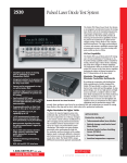
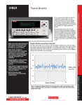
The Model 2520 Pulsed Laser Diode Test System
is an integrated, synchronized system for testing
laser diodes early in the manufacturing process,
when proper temperature control cannot be
easily achieved. The Model 2520 provides all
sourcing and measurement capabilities needed
for pulsed and continuous LIV (light-currentvoltage) testing of laser diodes in one compact,
half-rack instrument. The tight synchronization
of source and measure capabilities ensures high
measurement accuracy, even when testing with
pulse widths as short as 500ns.
LIV Test Capability
The Model 2520 can perform pulsed LIV testing
up to 5A and continuous LIV testing up to 1A.
Its pulsed testing capability makes it suitable for
testing a broad range of laser diodes, including
the pump laser designs for Raman amplifiers.
The instrument’s ability to perform both DC and
pulsed LIV sweeps on the same device simplifies
analyzing the impact of thermal transients on
the LIV characteristics of the laser diode.
• Simplifies laser diode LIV testing
prior to packaging or active
temperature control
• Integrated solution for in-process LIV
production testing of laser diodes at
the chip or bar level
• Sweep can be programmed to stop
on optical power limit
• Combines high accuracy source and
measure capabilities for pulsed and
DC testing
• Synchronized DSP based
measurement channels ensure highly
accurate light intensity and voltage
measurements
• Programmable pulse on time from
500ns to 5ms up to 4% duty cycle
• Pulse capability up to 5A, DC
capability up to 1A
• 14-bit measurement accuracy on
three measurement channels (V F,
front photodiode, back photodiode)
• Measurement algorithm increases
the pulse measurement’s signal-tonoise ratio
• Up to 1000-point sweep stored in
buffer memory eliminates GPIB
traffic during test, increasing
throughput
• Digital I/O binning and handling
operations
Maximize Throughput and
Eliminate Production Bottlenecks
By working in cooperation with leading laser
diode manufacturers, Keithley designed the
Model 2520 specifically to enhance chip- and
bar-level test stand yield and throughput. Its integrated design, ease of use, high speed, and high
accuracy provides a complete solution to help
laser diode manufacturers meet their production
schedules. Producers of laser diodes face constant pressure to increase test throughput and
Remote Electrical Test Head included
optimize return on investment for their capital
equipment used in production testing. Until
recently, these producers were forced to use relatively slow and cumbersome test stands for testing
laser diodes at the chip and bar level, which often led to production bottlenecks.
Higher Resolution for Higher Yields
To achieve the required signal-to-noise ratio,
traditional chip- and bar-level LIV testing solutions have required the use of boxcar averagers
or test system control software modifications to
allow averaging several pulsed measurements.
The resolution of these measurements is critical for the “kink” test and threshold current
calculations. With earlier test system designs,
particularly when performing the kink test,
low resolution and poor linearity of the analog
digitizer made it extremely difficult to discriminate between noise in the measurement and an
actual device kink. The Model 2520’s unique
DSP-based measurement approach automatically
APPLICATIONS
Production testing of:
• Telecommunication laser diodes
• Optical storage read/write head
laser diodes
• Vertical Cavity Surface-Emitting
Lasers (VCSELs)
• Thermal impedance
• Junction temperature response
• IEEE-488 and RS-232 interfaces
1.888.KEITHLEY (U.S. only)
w w w.keithley.com
Multi-channel pulsed
Side Text
test of laser diodes
Pulsed Laser Diode Test System
A
G R E A T E R
M E A S U R E
O F
C O N F I D E N C E
OPTOELECTRONICS TEST
2520
2520
Pulsed Laser Diode Test System
Ordering Information
2520
Pulsed Laser Diode
Test System with
Remote Test Head
Multi-channel pulsed
Side Text
test of laser diodes
2520/KIT1
Pulsed Laser Diode
Measurement Kit
(includes 2520, 2520INT,
and 3 ft. triax cable)
Accessories Supplied
User’s Manual, Quick Reference
Guide, Triax Cables (2),
BNC 10Ω Coaxial Cables (4)
ACCESSORIES AVAILABLE
2520INT-1-GE
7007-1
7007-2
KPCI-488LPA
KUSB-488B
Integrating Sphere (1 inch) with Germanium
Detector
Double Shielded GPIB Cable, 1m (3.3 ft.)
Double Shielded GPIB Cable, 2m (6.6 ft.)
IEEE-488 Interface/Controller for the PCI Bus
IEEE-488 USB-to-GPIB Adapter for USB Port
SERVICES AVAILABLE
2520-3Y-EW
1-year factory warranty extended to 3 years from
date of shipment
C/2520-3Y-DATA 3 (Z540-1 compliant) calibrations within 3 years
of purchase*
*Not available in all countries
identifies the settled region of the pulsed waveforms measured. This means the Model 2520 stores
only that portion of the pulse that is “flat” and contains meaningful data. All measurements made in
the flat portion of the pulse are averaged to improve the Signal-to-Noise ratio still further. If greater
resolution is required, the Model 2520 can be programmed to perform several pulse and measure
cycles at the same pulse amplitude. By making it possible to conduct more thorough testing at the
bar or chip level, the Model 2520 also eliminates the wasted time and costs associated with assembling then scrapping modules with non-compliant diodes.
Simple, One-Box Test Solution
The Model 2520 offers three channels of source and measurement circuitry. All three channels are
controlled by a single digital signal processor (DSP), which ensures tight synchronization of the
sourcing and measuring functions. The laser diode drive channel provides a current source coupled
with voltage measurement capability. Each of the two photodetector channels supplies an adjustable
voltage bias and voltage compliance, in addition to current measurement capability. These three
channels provide all the source and measure capabilities needed for full LIV characterization of laser
diodes prior to integration into temperature controlled modules. By eliminating the need for GPIB
commands to perform test sweeps with multiple separate instruments, the Model 2520’s integrated
sourcing and measurement allows a significant improvement in throughput.
Remote Test Head Maximizes Signal-to-Noise Ratio
The mainframe and remote test head architecture of the Model 2520 is designed to enhance pulsed
measurement accuracy, even at the sub-microsecond level. The remote test head ensures the measurement circuitry is located near the DUT, mounted on the fixture, minimizing cable effects. As the
schematic in Figure 1 shows, traditional semi-custom systems typically employed in the past require
significant integration. The architecture of the Model 2520 (Figure 2) offers a far more compact and
ready-to-use solution.
High Speed Pulse and Measure to Minimize Thermal Effects
The Model 2520 can accurately source and measure pulses as short as 500 nanoseconds to minimize
unwanted thermal effects during LIV testing. Users can program the pulse width from 500ns to 5ms
and pulse off time from 20µs to 500ms. There is a software duty cycle limit of 4% for currents higher
than 1A. To ensure greater accuracy, the instrument provides pulse width programming resolution
levels of 10µs (off time) and 100ns (on time).
Prior to the introduction of the Model 2520, test instrument limitations often placed barriers on test
performance. However, with the Model 2520, the limiting factor is not the test instrument, but the
Model 2520
High-Speed
Current to
Voltage
Converter
OPTOELECTRONICS TEST
Sequencing
and Signal
Analysis
Computer
High-Speed
Multi-Channel
Oscilloscope
Pulse
Source
GPIB
High-Speed
Current to
Voltage
Converter
High-Speed
Current to
Voltage
Converter
Front
Facet
Detector
Voltage Measure
Sequencing
and Signal
Analysis
DSP
Laser Diode
Chip or Bar
Rear
Facet
Detector
High-Speed
Multi-Channel
Digitizer
Pulse I
Source
Parallel Custom Bus
High-Speed
Current to
Voltage
Converter
Figure 1. This schematic reflects the current testing practices of
major laser diode manufacturers. Note that the use of discrete test
components increases the integration and programming effort, while
severely limiting the flexibility of the test system.
1.888.KEITHLEY (U.S. only)
w w w.keithley.com
Remote Test Head
2520INT
Laser Diode
Chip or Bar
Rear
Facet
Detector
Figure 2. The Model 2520 integrates synchronization, source, and
measure capabilities in a single half-rack instrument (with remote
test head) to provide maximum flexibility and test throughput.
A
G R E A T E R
M E A S U R E
O F
C O N F I D E N C E
2520
Pulsed Laser Diode Test System
ESD Protection
A laser diode’s material make-up, design, and small size make it extremely
sensitive to temperature increases and electrostatic discharges (ESDs). To
prevent damage, prior to the start of the test and after test completion, the
Model 2520 shorts the DUT to prevent transients from destroying the device.
The instrument’s 500 nanosecond pulse and measure test cycle minimizes
device heating during test, especially when a short duty cycle is used.
Test Sequencing and Optimization
Up to five user-definable test setups can be stored in the Model 2520 for easy
recall. The Model 2520’s built-in Buffer Memory and Trigger Link interface
can reduce or even eliminate time-consuming GPIB traffic during a test
sequence. The Buffer Memory can store up to 1000 points of measurement
data during the test sweep. The Trigger Link combines six independent software selectable trigger lines on a single connector for simple, direct control
over all instruments in a system. This interface allows the Model 2520 to
operate autonomously following an input trigger. The Model 2520 can be
programmed to output a trigger to a compatible OSA or wavelength meter
several nanoseconds prior to outputting a programmed drive current value
to initiate spectral measurements.
Figure 3. This plot illustrates the Model 2520’s pulsed LIV sweep capability. The sweep was programmed from 0 to 100mA in 1mA steps. Pulse
width was programmed at 1µs at 1% duty cycle, providing for a complete
sweep in just 10ms (excluding data transfer time).
Accessories and Options
The Model 2520 comes with all the interconnecting cables required for the
main instrument and the remote test head. Production test practices vary
widely (automated vs. semi-automated vs. manual), so the cable assemblies
from the remote test head to the DUT can vary significantly. To accommodate these differing requirements, Keithley has developed the Model 2520
RTH to DUT Cable Configuration Guide to help customers determine the
proper cable assemblies to use to connect the remote test head (RTH) to
the DUT.
Figure 4. Model 2520 Remote Test Head
Interface Options
The Model 2520 provides standard IEEE-488 and RS-232 interfaces to
speed and simplify system integration and control. A built-in digital I/O
interface can be used to simplify external handler control and binning
operations.
OPTOELECTRONICS TEST
Additional LIV Test Solutions
For production testing laser diodes after they have been packaged in
temperature controlled modules, Keithley offers the Laser Diode LIV Test
System with increased 28-bit core measurement resolution, allowing for
more detailed characterization. This flexible system combines all the DC
measurement capabilities required to test these modules with tight temperature control over the DUT in a modular instrument package. Configured
from proven Keithley instrumentation, the basic configuration can be easily
modified to add new measurement functions as new testing needs evolve.
1.888.KEITHLEY (U.S. only)
w w w.keithley.com
Multi-channel pulsed
Side Text
test of laser diodes
physics of the connections to the device. Keithley’s optoelectronics applications engineers have addressed these issues by studying and documenting
the optimum cable configuration to enhance measurement accuracy with
extremely fast pulses. Figure 3 illustrates the results of a typical pulse LIV
sweep test with the Model 2520. In this test, a 100-point pulsed LIV sweep
using a 1µs pulse width, at 1% duty cycle, was completed in just 110ms
(including data transfer time), several orders of magnitude faster than
existing, semi-custom test systems.
A
G R E A T E R
M E A S U R E
O F
C O N F I D E N C E
2520
Pulsed Laser Diode Test System
LASER DIODE PULSE OR DC CURRENT SOURCE SPECIFICATIONS
Model
Model
2520
Side
specifications
specifications
Text
DRIVE CURRENT
OFF CURRENT4
Source
Range
Programming
Resolution
Approx.
Electrical
Resolution
Accuracy1, 6
±(%rdg. + mA) 2, 3
RMS Noise
(typical)
(1kHz–20MHz)
0–500 mA
10 µA
8 µA
0.2 + 0.45
0–1.0 A DC
0–5.0 A Pulse
100 µA
80 µA
0.2 + 4.5
TEMPERATURE COEFFICIENT (0°–18°C & 28°–50°C): ±(0.15 × accuracy specification)/°C.
PULSE ON TIME19: 500ns to 5ms, 100ns programming resolution.
PULSE OFF TIME19: 20µs to 500ms, 10µs programming resolution.
PULSE DUTY CYCLE19, 20, 21: 0 to 99.6% for ≤1.0A; 0 to 4% for >1.0A.
VOLTAGE COMPLIANCE: 3V to 10V, 10mV programming resolution5.
POLARITY: 1 quadrant source, polarity reversal available through internal relay inversion.
OUTPUT OFF: <200mΩ short across laser diode; measured at Remote Test Head connector.
Approx.
Electrical
Resolution
Accuracy1
±(%rdg. + mA)
70 µA
0–15 mA
1 µA
7 nA typ.
0.2 + 0.45
800 µA
0–150 mA
10 µA
70 nA typ.
0.2 + 4.5
Setting and
Range
Load
7
Range
Accuracy
±(%rdg. + volts)1, 12
RMS Noise
(typical)13
5.00 V
0.33 mV
0.3% + 6.5 mV
60 µV
10.00 V
0.66 mV
0.3% + 8 mV
120 µV
RANGE: 0 to ±20VDC.
PROGRAMMING RESOLUTION: 10mV.
ACCURACY: ±(1% + 50mV).
CURRENT: 160mA max. with V-Bias shorted to I-Measure.
RMS NOISE (1kHz to 5MHz): 1mV typical.
PHOTODIODE CURRENT MEASURE SPECIFICATIONS
(each channel)
10.00 mA
20.00
mA
50.00
mA
100.00 mA
DC Input
Impedance
Accuracy
RMS Noise
±(%rdg. + current)1, 2 (typical) 3
0.7 µA
< 10 Ω
0.3% + 20 µA
90 nA
1.4 µA
< 6Ω
0.3% + 65 µA
180 nA
3.4 µA
< 3Ω
0.3% + 90 µA
420 nA
6.8 µA
<2.5 Ω
0.3% + 175 µA
840 nA
TEMPERATURE COEFFICIENT (0°–18°C & 28°–50°C): ±(0.15 × accuracy specification)/°C.
INPUT PROTECTION: The input is protected against shorting to the associated channel’s internal
bias supply. The input is protected for shorts to external supplies up to 20V for up to 1 second
with no damage, although calibration may be affected.
Number of
Source Points17
1
10 18
100 18
1000 18
1.888.KEITHLEY (U.S. only)
w w w.keithley.com
Typical
Max.
10 Ω 1⁄4 Watt
Fast
1.0%
55 ns
80 ns
500 mA
10 Ω 1⁄4 Watt
Slow
0.1%
1 µs
1.3 µs
5.00 A
1.5 Ω 1 Watt
Fast
1.0%
100 ns
130 ns
5.00 A
1.5 Ω 1 Watt
Slow
0.1%
1 µs
1.3 µs
SYSTEM SPEEDS
READING RATES (ms)15, 16
Rise/Fall Time6, 8, 9, 10
DC FLOATING VOLTAGE: User may float common ground up to ±10VDC from chassis
ground.
COMMON MODE ISOLATION: >109Ω.
OVERRANGE: 105% of range on all measurements and voltage compliance.
SOURCE OUTPUT MODES:
Fixed DC Level
Fixed Pulse Level
DC Sweep (linear, log, and list)
Pulse Sweep (linear, log, and list)
Continuous Pulse (continuous – low jitter)
PROGRAMMABILITY: IEEE-488 (SCPI-1995.0), RS-232, 5 user-definable power-up states plus
factory default and *RST.
DIGITAL INTERFACE:
Safety Interlock: External mechanical contact connector and removable key switch.
Aux. Supply: +5V @ 300mA supply.
Digital I/O: 2 trigger input, 4 TTL/Relay Drive outputs (33V @ 500mA max., diode
clamped).
Trigger Link: 6 programmable trigger input/outputs.
Pulse Trigger Out BNC: +5V, 50Ω output impedance, output trigger corresponding to
current source pulse; pulse to trigger delay <100ns. See Figure 3.
MAINS INPUT: 100V to 240V rms, 50–60Hz, 140VA.
EMC: Conforms to European Union Directive 89/336/EEC (EN61326-1).
SAFETY: Conforms to European Union Directive 73/23/EEC (EN61010-1) CAT 1.
VIBRATION: MIL-PRF-28800F Class 3, Random.
WARM-UP: 1 hour to rated accuracy.
DIMENSIONS, WEIGHT:
Main Chassis, bench configuration (with handle & feet): 105mm high × 238mm wide
× 416mm deep (41⁄8 in. × 93⁄8 in. × 163⁄8 in.). 2.67kg (5.90 lbs).
Remote Test Head: 95mm high × 178mm deep (with interlock key installed) × 216mm
wide (3½ in. × 7 in. × 8½ in.). 1.23kg (2.70 lbs).
ENVIRONMENT:
Operating: 0°–50°C, 70% R.H. up to 35°C. Derate 3% R.H./°C, 35°–50°C.
Storage: –25° to 65°C.
PHOTODIODE VOLTAGE BIAS SOURCE SPECIFICATIONS (each
channel)
Minimum
Resolution4
Pulse
Overshoot
Max.6, 8, 9
GENERAL
Minimum
Resolution
Range
Pulse
Mode
500 mA
LASER DIODE VOLTAGE MEASURE SPECIFICATIONS
TEMPERATURE COEFFICIENT (0°–18°C & 28°–50°C): ±(0.15 × accuracy specification)/°C.
MAX. LEAD RESOLUTION: 100Ω for rated accuracy.
INPUT IMPEDANCE: 2MΩ differential, 1MΩ from each input to common.
Input bias current ±7.5µA max.
OPTOELECTRONICS TEST
Range
Programming
Resolution
To
Memory
5.3
9.5
48
431
To
GPIB
6.8
18
120
1170
A
G R E A T E R
M E A S U R E
O F
C O N F I D E N C E
2520
Pulsed Laser Diode Test System
0.6
Full Pulse
0.5
1. 1 year, 23°C ±5°C.
2. If Duty Cycle · I exceeds 0.2, accuracy specifications must be derated with an additional error term as follows:
500mA Range: ±0.1% rdg. · D · I
5A Range:
±0.3% rdg. · D · I
where:
I = current setting
D = duty cycle
This derating must also be applied for a period equal to the time that D · I was ≥0.2.
3. Not including overshoot and setting time.
4. Pulse mode only.
5. Output: 500mA DC on 500mA range and 1A DC on 5A range.
6. Refer to Model 2520 Service Manual for test setup of current accuracy.
7. Figures 1 and 2 are typical pulse outputs into resistive loads.
8. Typical.
9. Per ANSI/IEEE Std 181-1977.
10. Per ANSI/IEEE Std 181-1977 10% to 90%.
11. DC accuracy ±700mV @ output terminal. 0.2Ω typical output impedance.
12. At DC, 10µs measurement pulse width, filter off.
13. Standard deviation of 10,000 readings with 10µs pulse width, filter off, with I source set to 0A DC.
14. The A/D converter has 14 bit resolution. The useful resolution is improved by reading averaging. The useful
resolution is:
0.515
0.51
0.4
0.505
Expanded Pulse Top
Current
0.3
(A)
Current
(A)
0.5
0.2
0.495
0.1
0.49
0.485
25
0
0
5
10
15
Time (μs)
20
Figure 1
Pulse Waveform Flatness - 5A into 2 Ohms
6
Full Pulse
5
5.04
4
5.02
Expanded Pulse Top
Current
3
(A)
5
2
4.98
1
4.96
0
0
5
Useful Resolution =
5.06
10
15
Time (μs)
20
Range
·
214
1
Pulse Width (ns) – 400ns
· Averaging Filter Setting
100ns
15. Excluding total programmed (Pulse ON time + Pulse OFF time).
16. Front panel off, calc off, filter off, duty cycle <10%, binary communications.
17. Returning 1 voltage and 2 current measurements for each source point.
18. Sweep mode.
19. Valid for both continuous pulse and sweep modes.
20. Shown is the Power Distribution % based on current settings.
21. Timing Cycle (pw⁄(pw + pd)): 4% max.
Current
(A)
Model
2520
specifications
Model
Side
specifications
Text
NOTES
Pulse Waveform Flatness - 500mA into 20 Ohms
4.94
25
Figure 2
Pulse Output/Trigger Output Relationship
6
Trigger
5
4
3
Volts
2
1
0
Pulse
-1
-2
-1.00E-06
-5.00E-07
0.00E+00
5.00E-07
1.00E-06
1.50E-06
OPTOELECTRONICS TEST
Time
Figure 3
1.888.KEITHLEY (U.S. only)
w w w.keithley.com
A
G R E A T E R
M E A S U R E
O F
C O N F I D E N C E