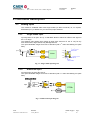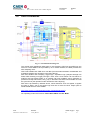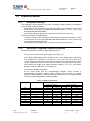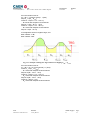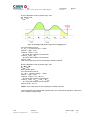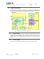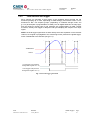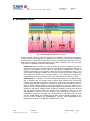
1
Technical Information Manual Revision n. 22 22 April 2013 MOD. V1720 8 CHANNEL 12 BIT 250 MS/S DIGITIZER MANUAL REV.22 NPO: 00103/05:V1720x.MUTx/22 CAEN will repair or replace any product within the guarantee period if the Guarantor declares that the product is defective due to workmanship or materials and has not been caused by mishandling, negligence on behalf of the User, accident or any abnormal conditions or operations. CAEN declines all responsibility for damages or injuries caused by an improper use of the Modules due to negligence on behalf of the User. It is strongly recommended to read thoroughly the CAEN User's Manual before any kind of operation. CAEN reserves the right to change partially or entirely the contents of this Manual at any time and without giving any notice. Disposal of the Product The product must never be dumped in the Municipal Waste. Please check your local regulations for disposal of electronics products. MADE IN ITALY : We stress the fact that all the boards are made in Italy because in this globalized world, where getting the lowest possible price for products sometimes translates into poor pay and working conditions for the people who make them, at least you know that who made your board was reasonably paid and worked in a safe environment. (this obviously applies only to the boards marked "MADE IN ITALY", we can not attest to the manufacturing process of "third party" boards). Document type: User's Manual (MUT) Title: Mod. V1720 8 Channel 12bit - 250MS/s Digitizer Revision date: 22/04/2013 Revision: 22 TABLE OF CONTENTS 1. 2. GENERAL DESCRIPTION .........................................................................................................................7 1.1. OVERVIEW ...............................................................................................................................................7 1.2. BLOCK DIAGRAM ...................................................................................................................................10 TECHNICAL SPECIFICATIONS ............................................................................................................11 2.1. PACKAGING AND COMPLIANCY ..............................................................................................................11 2.1.1. Supported VME Crates ..................................................................................................................11 2.1.2. Stand Alone operation ...................................................................................................................11 2.2. POWER REQUIREMENTS ..........................................................................................................................11 2.3. FRONT PANEL.........................................................................................................................................12 2.4. EXTERNAL CONNECTORS ........................................................................................................................13 2.4.1. ANALOG INPUT connectors .........................................................................................................13 2.4.2. CONTROL connectors ...................................................................................................................13 2.4.3. ADC REFERENCE CLOCK connectors .......................................................................................14 2.4.4. Digital I/O connectors ...................................................................................................................14 2.4.5. Optical LINK connector ................................................................................................................15 2.5. OTHER FRONT PANEL COMPONENTS .......................................................................................................16 2.5.1. Displays .........................................................................................................................................16 3. 2.6. INTERNAL COMPONENTS ........................................................................................................................17 2.7. TECHNICAL SPECIFICATIONS TABLE .......................................................................................................19 FUNCTIONAL DESCRIPTION................................................................................................................20 3.1. ANALOG INPUT.......................................................................................................................................20 3.1.1. Single ended input .........................................................................................................................20 3.1.2. Differential input ...........................................................................................................................20 3.2. CLOCK DISTRIBUTION ............................................................................................................................21 3.2.1. Direct Drive Mode .........................................................................................................................22 3.2.2. PLL Mode ......................................................................................................................................22 3.2.3. Trigger Clock .................................................................................................................................22 3.2.4. Output Clock ..................................................................................................................................22 3.2.5. AD9510 programming ...................................................................................................................22 3.2.6. PLL programming .........................................................................................................................22 3.2.7. Direct Drive BYPASS programming ..............................................................................................23 3.2.8. Configuration file ..........................................................................................................................23 3.2.9. Multiboard synchronization...........................................................................................................23 3.3. ACQUISITION MODES .............................................................................................................................24 3.3.1. Acquisition run/stop .......................................................................................................................24 3.3.2. Acquisition Triggering: Samples and Events .................................................................................24 3.3.2.1. 3.3.3. 3.3.3.1. Custom size events .................................................................................................................................... 26 Event structure ...............................................................................................................................26 Header ....................................................................................................................................................... 26 NPO: 00103/05:V1720x.MUTx/22 Filename: V1720_REV22 Number of pages: 61 Page: 3 Document type: User's Manual (MUT) 3.3.3.2. Revision date: 22/04/2013 Revision: 22 Samples ..................................................................................................................................................... 26 3.3.3.3. 3.3.4. Title: Mod. V1720 8 Channel 12bit - 250MS/s Digitizer Event format examples .............................................................................................................................. 27 Acquisition Synchronization ..........................................................................................................30 3.4. ZERO SUPPRESSION.................................................................................................................................31 3.4.1. Zero Suppression Algorithm ..........................................................................................................31 3.4.1.1. Full Suppression based on the amplitude of the signal .............................................................................. 31 3.4.1.2. 3.4.2. Zero Length Encoding ZLE....................................................................................................................... 32 Zero Suppression Examples...........................................................................................................33 3.5. TRIGGER MANAGEMENT .........................................................................................................................37 3.5.1. External trigger .............................................................................................................................37 3.5.2. Software trigger .............................................................................................................................37 3.5.3. Local channel auto-trigger ............................................................................................................38 3.5.3.1. 3.5.4. Trigger coincidence level .......................................................................................................................... 39 Trigger distribution .......................................................................................................................41 3.6. FRONT PANEL I/OS .................................................................................................................................42 3.6.1. Mode 0: REGISTER.......................................................................................................................44 3.6.2. Mode 1: TRIGGER ........................................................................................................................44 3.6.3. Mode 2: nBUSY/nVETO ................................................................................................................44 3.6.3.1. nBusy signal .............................................................................................................................................. 44 3.6.3.2. nVETO signal ............................................................................................................................................ 44 3.6.3.3. nTrigger signal .......................................................................................................................................... 44 3.6.3.4. 3.6.4. nRun signal................................................................................................................................................ 45 Mode 3: OLD STYLE .....................................................................................................................45 3.6.4.1. nClear_TTT signal .................................................................................................................................... 45 3.6.4.2. Busy signal ................................................................................................................................................ 45 3.6.4.3. DataReady signal ....................................................................................................................................... 45 3.6.4.4. Trigger signal ............................................................................................................................................ 45 3.6.4.5. Run signal.................................................................................................................................................. 45 3.7. ANALOG MONITOR .................................................................................................................................46 3.7.1. Trigger Majority Mode (Monitor Mode = 0) .................................................................................46 3.7.2. Test Mode (Monitor Mode = 1) .....................................................................................................47 3.7.3. Buffer Occupancy Mode (Monitor Mode = 3) ...............................................................................47 3.7.4. Voltage Level Mode (Monitor Mode = 4) ......................................................................................47 3.8. TEST PATTERN GENERATOR ....................................................................................................................47 3.9. RESET, CLEAR AND DEFAULT CONFIGURATION .....................................................................................48 3.9.1. Global Reset ..................................................................................................................................48 3.9.2. Memory Reset ................................................................................................................................48 3.9.3. Timer Reset ....................................................................................................................................48 3.10. VMEBUS INTERFACE .........................................................................................................................49 3.10.1. Addressing capabilities..................................................................................................................49 3.10.1.1. Base address.......................................................................................................................................... 49 3.10.1.2. CR/CSR address ................................................................................................................................... 49 NPO: 00103/05:V1720x.MUTx/22 Filename: V1720_REV22 Number of pages: 61 Page: 4 Document type: User's Manual (MUT) 3.10.1.3. 3.11. Title: Mod. V1720 8 Channel 12bit - 250MS/s Digitizer Revision date: 22/04/2013 Revision: 22 Address relocation ................................................................................................................................ 50 DATA TRANSFER CAPABILITIES ..........................................................................................................51 3.12. EVENTS READOUT ..............................................................................................................................51 3.12.1. Sequential readout .........................................................................................................................51 3.12.1.1. SINGLE D32 ........................................................................................................................................ 51 3.12.1.2. BLOCK TRANSFER D32/D64, 2eVME ............................................................................................. 52 3.12.1.3. CHAINED BLOCK TRANSFER D32/D64 ......................................................................................... 53 3.12.2. 3.13. Random readout (to be implemented) ............................................................................................53 OPTICAL LINK ....................................................................................................................................54 4. SOFTWARE TOOLS .................................................................................................................................55 5. INSTALLATION ........................................................................................................................................58 5.1. POWER ON SEQUENCE ...........................................................................................................................58 5.2. POWER ON STATUS ................................................................................................................................58 5.3. FIRMWARE UPGRADE ..............................................................................................................................59 5.3.1. V1720 Upgrade files description ...................................................................................................60 6. TECHNICAL SUPPORT ...........................................................................................................................61 LIST OF FIGURES FIG. 1.1: MOD. V1720 BLOCK DIAGRAM ...............................................................................................................10 FIG. 2.1: MOD. V1720 FRONT PANEL......................................................................................................................12 FIG. 2.2: MCX CONNECTOR ...................................................................................................................................13 FIG. 2.3: AMP DIFFERENTIAL CONNECTOR ............................................................................................................13 FIG. 2.4: AMP CLK IN/OUT CONNECTOR ............................................................................................................14 FIG. 2.5: PROGRAMMABLE IN/OUT CONNECTOR ..................................................................................................14 FIG. 2.6: LC OPTICAL CONNECTOR ........................................................................................................................15 FIG. 2.7: ROTARY AND DIP SWITCHES LOCATION ....................................................................................................18 FIG. 3.1: SINGLE ENDED INPUT DIAGRAM ...............................................................................................................20 FIG. 3.2: DIFFERENTIAL INPUT DIAGRAM ...............................................................................................................20 FIG. 3.3: CLOCK DISTRIBUTION DIAGRAM ..............................................................................................................21 FIG. 3.4: TRIGGER OVERLAP ..................................................................................................................................25 FIG. 3.5: EVENT ORGANIZATION (STANDARD MODE), NORMAL FORMAT ................................................................27 FIG. 3.6:EVENT ORGANIZATION (PACK2.5 MODE), NORMAL FORMAT ....................................................................28 FIG. 3.7: EVENT ORGANIZATION (STANDARD MODE), ZERO LENGTH ENCODING ...................................................28 FIG. 3.8: EVENT ORGANIZATION (PACK2.5 MODE), ZERO LENGTH ENCODING ......................................................29 FIG. 3.9: ZERO SUPPRESSION EXAMPLE ..................................................................................................................33 NPO: 00103/05:V1720x.MUTx/22 Filename: V1720_REV22 Number of pages: 61 Page: 5 Document type: User's Manual (MUT) Title: Mod. V1720 8 Channel 12bit - 250MS/s Digitizer Revision date: 22/04/2013 Revision: 22 FIG. 3.10: EXAMPLE WITH POSITIVE LOGIC AND NON-OVERLAPPING NLBK / NLFWD ................................................33 FIG. 3.11: EXAMPLE WITH NEGATIVE LOGIC AND NON-OVERLAPPING NLBK / NLFWD ..............................................34 FIG. 3.12: EXAMPLE WITH POSITIVE LOGIC AND NON OVERLAPPING NLBK..............................................................35 FIG. 3.13: EXAMPLE WITH POSITIVE LOGIC AND OVERLAPPING NLBK .....................................................................36 FIG. 3.14: BLOCK DIAGRAM OF TRIGGER MANAGEMENT ........................................................................................37 FIG. 3.15: LOCAL TRIGGER GENERATION ................................................................................................................38 FIG. 3.16: LOCAL TRIGGER RELATIONSHIP WITH MAJORITY LEVEL = 0 ..................................................................39 FIG. 3.17: LOCAL TRIGGER RELATIONSHIP WITH MAJORITY LEVEL = 1 AND TTVAW ≠ 0 ......................................40 FIG. 3.18: LOCAL TRIGGER RELATIONSHIP WITH MAJORITY LEVEL = 1 AND TTVAW = 0......................................41 FIG. 3.19: MAJORITY LOGIC (2 CHANNELS OVER THRESHOLD; BIT[6] OF CH. CONFIG. REGISTER =0) ....................46 FIG. 3.20: A24 ADDRESSING ...................................................................................................................................49 FIG. 3.21: A32 ADDRESSING ...................................................................................................................................49 FIG. 3.22: CR/CSR ADDRESSING ............................................................................................................................49 FIG. 3.23: SOFTWARE RELOCATION OF BASE ADDRESS ...........................................................................................50 FIG. 3.24: EXAMPLE OF BLT READOUT ..................................................................................................................52 FIG. 3.25: EXAMPLE OF RANDOM READOUT ...........................................................................................................53 FIG. 4.1: BLOCK DIAGRAM OF THE SOFTWARE LAYERS ..........................................................................................55 FIG. 4.2: WAVEDUMP OUTPUT WAVEFORMS ..........................................................................................................56 FIG. 4.3: CAENSCOPE OSCILLOSCOPE TAB ............................................................................................................56 FIG. 4.4: CAENUPGRADER GRAPHICAL USER INTERFACE.....................................................................................57 FIG. 4.5: DPP CONTROL SOFTWARE GRAPHICAL USER INTERFACE AND ENERGY PLOT ........................................57 LIST OF TABLES TABLE 1.1: AVAILABLE MODELS, RELATED PRODUCTS AND ACCESSORIES...............................................................8 TABLE 2.1: MOD. V1720 POWER REQUIREMENTS ..................................................................................................11 TABLE 2.2: FRONT PANEL LEDS ............................................................................................................................16 TABLE 2.3: MOD. V1720 TECHNICAL SPECIFICATIONS ...........................................................................................19 TABLE 3.1: BUFFER ORGANIZATION ......................................................................................................................24 TABLE 3.2: FRONT PANEL LVDS I/OS DEFAULT SETTING ......................................................................................42 TABLE 3.3: FEATURES DESCRIPTION WHEN LVDS GROUP IS CONFIGURED AS INPUT ...........................................43 TABLE 3.4: FEATURES DESCRIPTION WHEN LVDS GROUP IS CONFIGURED AS OUTPUT .......................................43 NPO: 00103/05:V1720x.MUTx/22 Filename: V1720_REV22 Number of pages: 61 Page: 6 Document type: User's Manual (MUT) Title: Mod. V1720 8 Channel 12bit - 250MS/s Digitizer Revision date: 22/04/2013 Revision: 22 1. General description 1.1. Overview The Mod. V1720 is a 1-unit wide VME 6U module housing a 8 Channel 12 bit 250MS/s Flash ADC Waveform Digitizer with 2 Vpp dynamic range on single ended MCX coaxial connectors. Versions featuring a 2 Vpp differential input full scale range are also available (see Table 1.1). For single ended versions, the DC offset is adjustable via a 16-bit DAC on each channel in the ±1 V range. The module features a front panel clock/reference In/Out and a PLL for clock synthesis from internal/external references. The data stream is continuously written in a circular memory buffer. When the trigger occurs, the FPGA writes further N samples for the post trigger and freezes the buffer that then can be read via VME or Optical Link. The acquisition can continue without dead-time in a new buffer. Each channel has a SRAM memory buffer (see Table 1.1 for the available memory sizes) divided in buffers of programmable size (1 – 1024). The readout (from VME or Optical link) of a frozen buffer is independent from the write operations in the active circular buffer (ADC data storage). Two modes are supported for the event storage in the board memories: Standard mode and Pack2.5 mode (see § 3.3.3). V1720 supports multi-board synchronization allowing all ADCs to be synchronized to a common clock source and ensuring Trigger time stamps alignment. Once synchronized, all data will be aligned and coherent across multiple V1720 boards VME and Optical Link accesses take place on independent paths and are handled by the on-board controller, therefore when accessed through Optical Link the board can be operated outside the VME Crate (see § 2.1). The trigger signal can be provided via the front panel input as well as via the software, but it can also be generated internally with threshold auto-trigger capability. The trigger from one board can be propagated to the other boards through the front panel TRG-OUT. An Analog Output allows to reproduce a Majority signal, a Test signal, a Buffer Occupancy signal and a programmable Voltage Level. The Modules VME interface is VME64X compliant and the data readout can be performed in Single Data Transfer (D32), 32/64 bit Block Transfer (BLT, MBLT, 2eVME, 2eSST) and 32/64 bit Chained Block Transfer (CBLT). The built-in daisy chainable Optical Link is able to transfer data at 80 MB/s, thus it is possible to connect up to eight V1720 (64 ADC channels) or thirty-two (256 ADC channels) to a single Optical Link Controller (Mod. A2818/A3818, see Table 1.1). NPO: 00103/05:V1720x.MUTx/22 Filename: V1720_REV22 Number of pages: 61 Page: 7 Document type: User's Manual (MUT) Title: Mod. V1720 8 Channel 12bit - 250MS/s Digitizer Revision date: 22/04/2013 Revision: 22 The V1720 can be controlled and readout through the Optical Link in parallel to the VME interface. CAEN provides also for this model a Digital Pulse Processing firmware for Physics Applications. This feature allows to perform on-line processing on detector signal directly digitized. V1720 is well suited for data acquisition and processing of signals from scintillators/photomultipliers or SiPM detectors, implementing function functionalities of a digital QDC Table 1.1: Available models, related products and accessories Code Description WV1720XAAAAA V1720 - 8 Ch. 12 bit 250 MS/s Digitizer: 1.25MS/ch, C4, SE WV1720BXAAAA V1720B - 8 Ch. 12 bit 250 MS/s Digitizer: 10MS/ch, C4, SE WV1720CXAAAA V1720C - 8 Ch. 12 bit 250 MS/s Digitizer: 1.25MS/ch, C4, DIFF WV1720DXAAAA V1720D - 8 Ch. 12 bit 250 MS/s Digitizer: 10MS/ch, C4, DIFF WV1720EXAAAA V1720E - 8 Ch. 12 bit 250 MS/s Digitizer: 1.25MS/ch, C20, SE WV1720FXAAAA V1720F - 8 Ch. 12 bit 250 MS/s Digitizer: 1.25MS/ch, C20, DIFF WV1720GXAAAA V1720G - 8 Ch. 12 bit 250 MS/s Digitizer: 10MS/ch, C20, SE WVX1720XAAAA VX1720 - 8 Ch. 12 bit 250 MS/s Digitizer: 1.25MS/ch, C4, SE WVX1720BXAAA VX1720B - 8 Ch. 12 bit 250 MS/s Digitizer: 10MS/ch, C4, SE WVX1720CXAAA VX1720C - 8 Ch. 12 bit 250 MS/s Digitizer: 1.25MS/ch, C4, DIFF WVX1720DXAAA VX1720D - 8 Ch. 12 bit 250 MS/s Digitizer: 10MS/ch, C4, DIFF WVX1720EXAAA VX1720E - 8 Ch. 12 bit 250 MS/s Digitizer: 1.25MS/ch, C20, SE WVX1720FXAAA VX1720F - 8 Ch. 12 bit 250 MS/s Digitizer: 1.25MS/ch, C20, DIFF WA654XAAAAAA A654 - Single Channel MCX to LEMO Cable Adapter WA654K4AAAAA A654 KIT4 - 4 MCX TO LEMO Cable Adapter WA654K8AAAAA A654 KIT8 - 8 MCX TO LEMO Cable Adapter WA659XAAAAAA A659 - Single Channel MCX to BNC Cable Adapter WA659K4AAAAA A659 KIT4 - 4 MCX TO BNC Cable Adapter WA659K8AAAAA A659 KIT8 - 8 MCX TO BNC Cable Adapter WV1718XAAAAA V1718 - VME-USB 2.0 Bridge WV1718LCXAAA V1718LC - VME-USB 2.0 Bridge (Rohs Compliant) WVX1718XAAAA VX1718 - VME-USB 2.0 Bridge WVX1718LCXAA VX1718LC - VME-USB 2.0 Bridge WV2718XAAAAA V2718 - VME-PCI Bridge WV2718LCXAAA V2718LC - VME-PCI Bridge (Rohs compliant) WK2718LCXAAA V2718KITLC - VME-PCI Bridge (V2718)+PCI Optical Link (A2818)+Optical Fibre 5m duplex (AY2705) (Rohs) WK2718XAAAAA V2718KIT - VME-PCI Bridge (V2718) + PCI OpticalLink (A2818) + Optical Fibre 5m duplex (AY2705) WK2718XBAAAA V2718KITB - VME-PCI Bridge (V2718) + PCIe Optical Link (A3818A) + Optical Fibre 5m duplex (AY2705) WVX2718LCXAA VX2718LC - VME-PCI Bridge WVX2718XAAAA VX2718 - VME-PCI Bridge WKX2718XAAAA VX2718KIT - VME-PCI Bridge (VX2718) + PCI OpticalLink (A2818) + Optical Fibre 5m duplex (AY2705) WKX2718XBAAA VX2718KITB - VME-PCI Bridge (VX2718) + PCIe Optical Link (A3818A) + Optical Fibre 5m duplex (AY2705) WKX2718LCXAA VX2718KITLC - VME-PCI Bridge (VX2718) + PCI Optical Link (A2818) + Optical Fibre 5m duplex (AY2705) NPO: 00103/05:V1720x.MUTx/22 Filename: V1720_REV22 Number of pages: 61 Page: 8 Document type: User's Manual (MUT) Title: Mod. V1720 8 Channel 12bit - 250MS/s Digitizer WA2818XAAAAA A2818 - PCI Optical Link WA3818AXAAAA A3818A - PCIe 1 Optical Link WA3818BXAAAA A3818B - PCIe 2 Optical Link WA3818CXAAAA A3818C - PCIe 4 Optical Link WA317XAAAAAA A317 - Clock Distribution Cable WAI2730XAAAA AI2730 - Optical Fibre 30 m. simplex WAI2720XAAAA AI2720 - Optical Fibre 20 m. simplex WAI2705XAAAA AI2705 - Optical Fibre 5 m. simplex Revision date: 22/04/2013 Revision: 22 WAI2703XAAAA AI2703 - Optical Fibre 30cm. simplex WAY2730XAAAA AY2730 - Optical Fibre 30 m. duplex WAY2720XAAAA AY2720 - Optical Fibre 20 m. duplex WAY2705XAAAA AY2705 - Optical Fibre 5 m. duplex WFWDPPCIAAAA DPP-CI - Digital Pulse Processing for Charge Integrationon for (x720) WFWDPPCI02AA DPP-CI - Digital Pulse Processing for Charge Integration for (x720) - 2 Licence Pack WFWDPPCI05AA DPP-CI - Digital Pulse Processing for Charge Integration for (x720) - 5 Licence Pack WFWDPPCI10AA DPP-CI - Digital Pulse Processing for Charge Integration for (x720) - 10 Licence Pack WFWDPPCI20AA DPP-CI - Digital Pulse Processing for Charge Integration for (x720) - 20 Licence Pack WFWDPPNGAA20(*) DPP-PSD - Digital Pulse Processing for Pulse Shape Discrimination for (x720) WFWDPPNG0220(*) DPP-PSD - Digital Pulse Processing for Pulse Shape Discrimination for (x720) - 2 Licence Pack WFWDPPNG0520(*) DPP-PSD - Digital Pulse Processing for Pulse Shape Discrimination for (x720) - 5 Licence Pack WFWDPPNG1020(*) DPP-PSD - Digital Pulse Processing for Pulse Shape Discrimination for (x720) - 10 Licence Pack WFWDPPNG2020(*) DPP-PSD - Digital Pulse Processing for Pulse Shape Discrimination (x720) - 20 Licence Pack (*) The DPP-PSD firmware runs only on V1720E/V1720F/V1720G NPO: 00103/05:V1720x.MUTx/22 Filename: V1720_REV22 Number of pages: 61 Page: 9 Document type: User's Manual (MUT) Title: Mod. V1720 8 Channel 12bit - 250MS/s Digitizer Revision date: 22/04/2013 Revision: 22 1.2. Block Diagram FRONT PANEL x8 channels DAC AMC [FPGA] ADC & MEMORY CONTROLLER MUX OSC CLK IN CLOCK MANAGER (AD9510) CLK OUT VCXO 1GHz LOCAL BUS BUFFERS VME ADC TRIGGERS & SYNC INPUTS TRG IN TRG OUT S IN MON DIGITAL I/Os DAC ROC [FPGA] - Readout control - VME interface control - Optical link control - Trigger control - External interface control OPTICAL LINK Fig. 1.1: Mod. V1720 Block Diagram The function of each block will be explained in detail in the subsequent sections. NPO: 00103/05:V1720x.MUTx/22 Filename: V1720_REV22 Number of pages: 61 Page: 10 Document type: User's Manual (MUT) Title: Mod. V1720 8 Channel 12bit - 250MS/s Digitizer Revision date: 22/04/2013 Revision: 22 2. Technical specifications 2.1. Packaging and Compliancy 2.1.1. Supported VME Crates The module is housed in a 6U-high, 1U-wide VME unit. The board hosts the VME P1, and P2 connectors and fits into both VME/VME64 standard and V430 backplanes. VX1720 versions fit VME64X compliant crates. 2.1.2. Stand Alone operation When accessed through Optical Link (see § 3.13) the board can be operated outside the VME Crate. It is up to the User to provide the required power supplies (see § 2.2) and adequate cooling ventilation. 2.2. Power requirements The power requirements of the module are as follows: Table 2.1: Mod. V1720 power requirements NPO: 00103/05:V1720x.MUTx/22 Filename: V1720_REV22 +5 V 4.0 A +12 V 0.2 A -12 V 0.2 A Number of pages: 61 Page: 11 Document type: User's Manual (MUT) Title: Mod. V1720 8 Channel 12bit - 250MS/s Digitizer Revision date: 22/04/2013 Revision: 22 2.3. Front Panel Mod. V560E Mod. V1720 EXTERNAL CLOCK IN INTERNAL CLOCK OUT LOCAL TRIGGER OUT EXTERNAL TRIGGER IN SYNC/SAMPLE START ANALOG INPUT ANALOG MONITOR OUTPUT DIGITAL I/O's SCALER 8 CH 12 BIT 250 MS/S DIGITIZER Fig. 2.1: Mod. V1720 front panel NPO: 00103/05:V1720x.MUTx/22 Filename: V1720_REV22 Number of pages: 61 Page: 12 Document type: User's Manual (MUT) Title: Mod. V1720 8 Channel 12bit - 250MS/s Digitizer Revision date: 22/04/2013 Revision: 22 2.4. External connectors 2.4.1. ANALOG INPUT connectors Fig. 2.2: MCX connector Single ended version (see options in § 1.1): Function: Analog input, single ended, input dynamics: 2Vpp Zin=50 Mechanical specifications: MCX connector (CS 85MCX-50-0-16 SUHNER) Fig. 2.3: AMP Differential connector Differential version (see options in § 1.1): Function: Analog input, differential, input dynamics: 2.25Vpp Zin=100 or 10Vpp Zin=1K Mechanical specifications: AMP 3-102203-4 AMP MODUII 2.4.2. CONTROL connectors Function: TRG OUT: Local trigger output (NIM/TTL, on Rt = 50Ω) TRG IN: External trigger input (NIM/TTL, Zin= 50Ω) SYNC/SAMPLE/START: Sample front panel input (NIM/TTL, Zin=50Ω) MON/Σ: DAC output 1Vpp on Rt=50Ω Mechanical specifications: 00-type LEMO connectors NPO: 00103/05:V1720x.MUTx/22 Filename: V1720_REV22 Number of pages: 61 Page: 13 Document type: User's Manual (MUT) 2.4.3. Title: Mod. V1720 8 Channel 12bit - 250MS/s Digitizer Revision date: 22/04/2013 Revision: 22 ADC REFERENCE CLOCK connectors GND CLKCLK+ Fig. 2.4: AMP CLK IN/OUT Connector Function: CLK IN: External clock/Reference input, AC coupled (diff. LVDS, ECL, PECL, LVPECL, CML), Zdiff= 110. Mechanical specifications: AMP 3-102203-4 connector Function: CLOCK OUT: Clock output, DC coupled (diff. LVDS), Zdiff= 110. Mechanical specifications: AMP 3-102203-4 AMP MODUII 2.4.4. Digital I/O connectors Fig. 2.5: Programmable IN/OUT Connector Function: N.16 programmable differential LVDS I/O signals, Zdiff_in= 110 Ohm. Four Indipendent signal group 03, 47, 811, 1215, In / Out direction control; see also § 3.6. Mechanical specifications: 3M-7634-5002- 34 pin Header Connector NPO: 00103/05:V1720x.MUTx/22 Filename: V1720_REV22 Number of pages: 61 Page: 14 Document type: User's Manual (MUT) 2.4.5. Title: Mod. V1720 8 Channel 12bit - 250MS/s Digitizer Revision date: 22/04/2013 Revision: 22 Optical LINK connector Fig. 2.6: LC Optical Connector Mechanical specifications: LC type connector; to be used with Multimode 62.5/125µm cable with LC connectors on both sides Electrical specifications: Optical link for data readout and slow control with transfer rate up to 80MB/s; daisy chainable. NPO: 00103/05:V1720x.MUTx/22 Filename: V1720_REV22 Number of pages: 61 Page: 15 Document type: User's Manual (MUT) Title: Mod. V1720 8 Channel 12bit - 250MS/s Digitizer Revision date: 22/04/2013 Revision: 22 2.5. Other front panel components 2.5.1. Displays The front panel hosts the following LEDs: Table 2.2: Front panel LEDs Name: DTACK CLK_IN NIM TTL LINK PLL _LOCK PLL _BYPS Colour: green green green green green/yellow green green RUN TRG DRDY BUSY OUT_LVDS green green green red green NPO: 00103/05:V1720x.MUTx/22 Function: VME read/write access to the board External clock enabled. Standard selection for CLK I/O, TRG OUT, TRG IN, S IN. Standard selection for CLK I/O, TRG OUT, TRG IN, S IN. Network present; Data transfer activity The PLL is locked to the reference clock The reference clock drives directly ADC clocks; the PLL circuit is switched off and the PLL_LOCK LED is turned off. RUN bit set Triggers are accepted Event/data (depending on acquisition mode) are present in the Output Buffer All the buffers are full Signal group OUT direction enabled. Filename: V1720_REV22 Number of pages: 61 Page: 16 Document type: User's Manual (MUT) Title: Mod. V1720 8 Channel 12bit - 250MS/s Digitizer Revision date: 22/04/2013 Revision: 22 2.6. Internal components SW2,4,5,6 “Base Addr. [31:16]”: Type: 4 rotary switches Function: Set the VME base address of the module. SW3 “CLOCK SOURCE” Type Dip Switch Function: Select clock source (External or Internal) SW1 “FW” Type: Dip Switch. Function: it allows to select whether the “Standard” (STD) or the “Back up” (BKP) firmware must be loaded at power on; (default position: STD). NPO: 00103/05:V1720x.MUTx/22 Filename: V1720_REV22 Number of pages: 61 Page: 17 Document type: User's Manual (MUT) Title: Mod. V1720 8 Channel 12bit - 250MS/s Digitizer Revision date: 22/04/2013 Revision: 22 Fig. 2.7: Rotary and dip switches location NPO: 00103/05:V1720x.MUTx/22 Filename: V1720_REV22 Number of pages: 61 Page: 18 Document type: User's Manual (MUT) Title: Mod. V1720 8 Channel 12bit - 250MS/s Digitizer Revision date: 22/04/2013 Revision: 22 2.7. Technical specifications table Table 2.3: Mod. V1720 technical specifications Package 1-unit wide VME 6U module Analog Input 8 channels, single-ended (SE) or differential. Input range: 2 Vpp; Bandwidth: 125 MHz. Programmable DAC for Offset Adjust x ch. (SE only). Digital Conversion Resolution: 12 bit; Sampling rate: 31.25 to 250 MS/s simultaneously on each channel; multi board synchronization (one board can act as clock master). External Gate Clock capability (NIM/TTL) for burst or single sampling mode. ADC Sampling Clock generation Three operating modes: - PLL mode - internal reference (50 MHz loc. oscillator). - PLL mode - external reference on CLK_IN (Jitter<100ppm). - PLL Bypass mode: Ext. clock on CLK_IN drives directly ADC clocks (Freq.: 31.25 ÷ 250 MHz). CLK_IN AC coupled differential input clock LVDS, ECL, PECL, LVPECL, CML CLK_OUT DC coupled differential LVDS output clock, locked to ADC sampling clock. Freq.: 31.25 ÷ 250MHz. Memory Buffer 1.25 M sample/ch (on V1720 / VX1720 / V1720C / VX1720C / V1720E / VX1720E / V1720F / VX1720F) or 10 M sample/ch (V1720B / VX1720B / V1720D / VX1720D); Multi Event Buffer with independent read and write access. Programmable event size and pre-post trigger. Divisible into 1 ÷ 1024 buffers. Trigger Common External TRGIN (NIM or TTL) and VME CommandIndividual channel autotrigger (time over/under threshold)TRGOUT (NIM or TTL) for the trigger propagation to other V1720 boards. Trigger Time Stamp 31-bit counter – 8ns resolution – 34s range. ADC and Memory controller FPGA One Altera Cyclone EP1C4 or EP1C20 per couple of channels (see Table 1.1). Optical Link Data readout and slow control with transfer rate up to 80 MB/s, to be used instead of VME bus. Daisy chainable: A2818 (PCI) and A3818 (PCIe) cards can control and read respectively up to eight and thirty-two V1720 boards in a chain. VME interface VME64X compliant D32, BLT32, MBLT64, CBLT32/64, 2eVME, 2eSST, Multi Cast Cycles. Transfer rate: 60MB/s (MBLT64), 100MB/s (2eVME), 160MB/s (2eSST). Sequential and random access to the data of the Multi Event Buffer. The Chained readout allows to read one event from all the boards in a VME crate with a BLT access. Upgrade V1720 firmware can be upgraded via VME Software General purpose C Libraries and Demo Programs Zero Suppression - Full Suppression based on the signal amplitude (ZS_AMP) - Zero Length Encoding (ZLE); see § 3.3.4 Analog Monitor 12bit / 125MHz DAC FPGA controlled, four operating modes: - Waveform Generator: 1 Vpp ramp generator. - Majority: output signal is proportional to the number of ch. under/over threshold (1 step = 125mV). - Buffer Occupancy: output signal is proportional to the Multi Event Buffer Occupancy: 1 buffer ~ 1mV. - Voltage level: output signal is a programmable voltage level. LVDS I/O 16 general purpose LVDS I/O controlled by the FPGA Busy, Data Ready, Memory full, Individual Trig-Out and other function can be programmed An Input Pattern from the LVDS I/O can be associated to each trigger as an event marker 1 1 Available with Piggy Back Rev. 0.5 and Firmware Rev. 0.5 (and later) NPO: 00103/05:V1720x.MUTx/22 Filename: V1720_REV22 Number of pages: 61 Page: 19 Document type: User's Manual (MUT) Title: Mod. V1720 8 Channel 12bit - 250MS/s Digitizer Revision date: 22/04/2013 Revision: 22 3. Functional description 3.1. Analog Input The module is available either with single ended (on MCX connector) or, on request, differential (on Tyco MODU II 3-pin connector) input channels. 3.1.1. Single ended input Input dynamics is 2V (Zin= 50 ). A 16bit DAC allows to add a DC offset to the signal in the ±1 V range. The absolute max analog input voltage is 6Vpp (with Vrail max of +6V or -6V) for any DAC offset value; larger values may damage the unit. st The input bandwidth ranges from DC to 250 MHz (with 1 order anti-aliasing low pass filter). Input Dynamic Range: 1 Vpp MCX OpAmp Input 50 ADC +1.00 8 bit Positive Unipolar DAC = FSR +0.50 FPGA Vref DAC 0 +0.50 16 bit -1.00 Negative Unipolar DAC = 0 Bipolar DAC = FSR/2 Fig. 3.1: Single ended input diagram 3.1.2. Differential input Input dynamics is 2Vpp (Zin= 50 ). st The input bandwidth ranges from DC to 250 MHz (with 1 order anti-aliasing low pass filter). Differential Mode Input Zdiff OpAmp ADC AMP MODUII Vref 12 bit FPGA DAC Fig. 3.2: Differential input diagram NPO: 00103/05:V1720x.MUTx/22 Filename: V1720_REV22 Number of pages: 61 Page: 20 Document type: User's Manual (MUT) Title: Mod. V1720 8 Channel 12bit - 250MS/s Digitizer Revision date: 22/04/2013 Revision: 22 3.2. Clock Distribution Fig. 3.3: Clock distribution diagram The module clock distribution takes place on two domains: OSC-CLK and REF-CLK; the former is a fixed 50MHz clock provided by an on board oscillator, the latter provides the ADC sampling clock. OSC-CLK handles both VME and Local Bus (communication between motherboard and mezzanine boards; see red traces in the figure above). REF-CLK handles ADC sampling, trigger logic, acquisition logic (samples storage into RAM, buffer freezing on trigger) through a clock chain. Such domain can use either an external (via front panel signal) or an internal (via local oscillator) source (selection is performed via dip switch SW1, see § 2.6); in the latter case OSC-CLK and REF-CLK will be synchronous (the operation mode remains the same anyway). REF-CLK is processed by AD9510 device, which delivers 6 clock out signals; 4 signals are sent to ADCs, one to the trigger logic and one to drive CLK-OUT output (refer to AD9510 data sheet for more details: http://www.analog.com/UploadedFiles/Data_Sheets/AD9510.pdf ); two operating modes are foreseen: Direct Drive Mode and PLL Mode NPO: 00103/05:V1720x.MUTx/22 Filename: V1720_REV22 Number of pages: 61 Page: 21 Document type: User's Manual (MUT) 3.2.1. Title: Mod. V1720 8 Channel 12bit - 250MS/s Digitizer Revision date: 22/04/2013 Revision: 22 Direct Drive Mode The aim of this mode is to drive externally the ADCs' Sampling Clock; generally this is necessary when the required sampling frequency is not a VCXO frequency submultiple. The only requirement over the SAMP-CLK is to remain within the ADCs' range. 3.2.2. PLL Mode The AD9510 features an internal Phase Detector which allows to couple REF-CLK with VCXO (1 GHz frequency); for this purpose it is necessary that REF-CLK is a submultiple of 1 GHz. AD9510 default setting foresees the board internal clock (50MHz) as clock source of REF-CLK. This configuration leads to Ndiv = 100, Rdiv = 5, thus obtaining 10MHz at the Phase Detector input and CLK-INT = 1GHz. The required 250 MHz Sampling Clock is obtained by processing CLK-INT through Sdiv dividers. When an external clock source is used, if it has 50MHz frequency, then AD9510 programming is not necessary, otherwise Ndiv and Rdiv have to be modified in order to achieve PLL lock. A REF-CLK frequency stability better than 100ppm is mandatory. 3.2.3. Trigger Clock TRG-CLK signal has a frequency equal to ½ of SAMP-CLK; therefore a 2 samples “uncertainty” occurs over the acquisition window. 3.2.4. Output Clock Front panel Clock Output is User programmable. Odiv and Odel parameters allows to obtain a signal with the desired frequency and phase shift (in order to recover cable line delay) and therefore to synchronise daisy chained boards. CLK-OUT default setting is OFF, it is necessary to enable the AD9510 output buffer to enable it. 3.2.5. AD9510 programming CAEN has developed a software tool which allows to handle easily the clock parameters, the CAENupgrader; see www.caen.it path: Products / Front End / VME / Controller (VME) 3.2.6. PLL programming In PLL mode the User has to enter the divider for input clock frequency (input clock PLL mode, via CAENupgrader); since the VCXO frequency is 1GHz, in order to use, for example, a 50MHz ExtClk, the divider to be entered is 20. Then it is necessary to set the parameters for sampling clock and CLK_OUT (enable, frequency and delay in Output Clock field via CAENupgrader); the tool refuses wrong settings for such parameters. NPO: 00103/05:V1720x.MUTx/22 Filename: V1720_REV22 Number of pages: 61 Page: 22 Document type: User's Manual (MUT) 3.2.7. Title: Mod. V1720 8 Channel 12bit - 250MS/s Digitizer Revision date: 22/04/2013 Revision: 22 Direct Drive BYPASS programming In BYPASS mode, the User can directly set the input frequency (Input Clock field, real values are allowed). Given an input frequency, it is possible to set the parameters in order to provide the required signals. 3.2.8. Configuration file Once all parameters are set, the tool allows to save the configuration file which includes all the AD9510 device settings (see CAENupgrader documentation). It is also possible to browse and load into the AD9510 device a pre existing configuration file (see CAENupgrader documentation). For this purpose it is not necessary the board power cycle. 3.2.9. Multiboard synchronization In cases when multi-board systems are involved in an experiment, it is necessary to synchronize different boards. In this way the user can acquire from N boards with Y channel each, like if they were just one board with (N x Y) channels. The main issue in the synchronization of a multi-board system is to propagate the sampling clock among the boards. This is made through input/output daisy chain connections among the digitizers. One board has to be chosen to be the “master” board that propagates its own clock to the others. A programmable phase shift can adjust possible delays in the clock propagation. This allows to have both the same ADC sampling clock, and the same time reference for all boards. Having the same time reference means that the acquisition starts/stops at the same time, and that the time stamps of different boards is aligned to the same absolute time. There are several ways to implement the trigger logic. The synchronization tool allows to propagate the trigger to all boards and acquire the events accordingly. Moreover, in case of busy state of one or more boards, the acquisition is inhibited for all boards. For a detailed guide to multi-board synchronization, refer to the document: AN2086 - Synchronization of CAEN Digitizers in Multiple Board Acquisition Systems (web available). NPO: 00103/05:V1720x.MUTx/22 Filename: V1720_REV22 Number of pages: 61 Page: 23 Document type: User's Manual (MUT) Title: Mod. V1720 8 Channel 12bit - 250MS/s Digitizer Revision date: 22/04/2013 Revision: 22 3.3. Acquisition Modes 3.3.1. Acquisition run/stop The acquisition can be started in two ways, according to bits[1:0] setting of Acquisition Control register (address 0x8100): setting bit[2] in the Acquisition Control register (bits[1:0] of Acquisition Control must be set to 00, that is SW CONTROLLED Start/Stop Mode, or to 01, that is S-IN CONTROLLED Start/Stop Mode). driving S-IN signal high (bits[1:0] of Acquisition Control must be set to 01) Therefore acquisition is stopped either: resetting the bit[2] in the Acquisition Control register (bits[1:0] of Acquisition Control must be set to 00, that is SW CONTROLLED Start/Stop Mode, or to 01, that is S-IN CONTROLLED Start/Stop Mode). driving S-IN signal low (bits[1:0] of Acquisition Control must be set to 01). 3.3.2. Acquisition Triggering: Samples and Events When the acquisition is running, a trigger signal allows to: store a 31-bit counter value of the Trigger Time Tag (TTT). The counter (representing a time reference), like so the Trigger Logic Unit (see § 3.2) operates at a frequency of 125 MHz (i.e. 8 ns, that is to say 2 ADC clock cycles). Due to the way the acquired data are written into the board internal memory (i.e in 4-sample bunches), the TTT counter is read every 2 trigger logic clock cycles, which means the trigger time stamp resolution results in 16 ns (i.e. 62.5 MHz). Basing on that, the LSB of the TTT is always “0”. increment the EVENT COUNTER; fill the active buffer with the pre/post-trigger samples, whose number is programmable (Acquisition window width), freezing then the buffer for readout purposes, while acquisition continues on another buffer buffer size is programmable through the Buffer Organization (0x800C) register. Table 3.1: Buffer Organization REGISTER 0x00 0x01 0x02 0x03 0x04 0x05 0x06 0x07 0x08 0x09 0x0A NPO: 00103/05:V1720x.MUTx/22 BUFFER NUMBER 1 2 4 8 16 32 64 128 256 512 1024 Filename: V1720_REV22 SIZE of one BUFFER (samples) SRAM 1.25 MB/ch Std. Pack2.5 1M 1.25M 512K 640K 256K 320K 128K 160K 64K 80K 32K 40K 16K 20K 8K 10K 4K 5K 2K 2.5K 1K 1.25K SRAM 10 MB/ch Std. Pack2.5 8M 10M 4M 5M 2M 2.5M 1M 1.25M 512K 640K 256K 320K 128K 160K 64K 80K 32K 40K 16K 20K 8K 10K Number of pages: 61 Page: 24 Document type: User's Manual (MUT) Title: Mod. V1720 8 Channel 12bit - 250MS/s Digitizer Revision date: 22/04/2013 Revision: 22 An event is therefore composed by the trigger time tag, pre- and post-trigger samples and the event counter. Overlap between “acquisition windows” may occur (a new trigger occurs while the board is still storing the samples related to the previous trigger); this overlap can be either rejected or accepted (programmable via VME). If the board is programmed to accept the overlapped triggers, as the “overlapping” trigger arrives, the current active buffer is filled up, then the samples storage continues on the subsequent one. In this case events will not have all the same size (see Fig. 3.4). EVENT n EVENT n+1 EVENT n+2 Recorded Not Recorded TRIGGER PRE POST ACQUISITION WINDOW Overlapping Triggers Fig. 3.4: Trigger Overlap A trigger can be refused for the following causes: acquisition is not active memory is FULL and therefore there are no available buffers the required number of samples for building the pre-trigger of the event is not reached yet; this happens typically as the trigger occurs too early either with respect to the RUN_ACQUISITION command (see § 3.3.1) or with respect to a buffer emptying after a MEMORY_FULL status the trigger overlaps the previous one and the board is not enabled for accepting overlapped triggers As a trigger is refused, the current buffer is not frozen and the acquisition continues writing on it. The Event Counter can be programmed in order to be either incremented or not. If this function is enabled, the Event Counter value identifies the number of the triggers sent (but the event number sequence is lost); if the function is not enabled, the Event Counter value coincides with the sequence of buffers saved and readout. NPO: 00103/05:V1720x.MUTx/22 Filename: V1720_REV22 Number of pages: 61 Page: 25 Document type: User's Manual (MUT) Title: Mod. V1720 8 Channel 12bit - 250MS/s Digitizer 3.3.2.1. Revision date: 22/04/2013 Revision: 22 Custom size events It is possible to make events with a number of Memory locations, which depends on Buffer Organization register setting, smaller than the default value. One memory location contains two ADC samples and the maximum number of memory locations NLOC is therefore half the maximum number of samples per block NS = 512K/Nblocks (640K/Nblocks when Pack2.5 mode is used). Smaller NLOC values can be achieved by writing the number of locations NLOC into the Custom Size. NLOC = 0 means “default size events”, i.e. the number of memory locations is the maximum allowed. NLOC = N1, with the constraint 0<N1<½NS (0<N1<2/5NS with Pack2.5), means that one event will be made of 2N1 samples (2.5N1 samples with Pack2.5). 3.3.3. Event structure An event is structured as follows: Header (four 32-bit words) Data (variable size and format) The event can be readout either via VME or Optical Link; data format is 32 bit long word, therefore each long_word contains 4 samples. 3.3.3.1. Header It is composed by four words, namely: Size of the event (number of 32-bit long words) Board ID (GEO); Bit24; data format: 0= normal format; 1= Zero Length Encoding data compression method enabled; 16 bit pattern, latched on the LVDS I/O as one trigger arrives; Channel Mask (=1: channels participating to event; ex CH5 and CH7 participating→Ch Mask: 0xA0, this information must be used by the software to acknowledge which channel the samples are coming from) Event Counter: It is the trigger counter; it can count either accepted triggers only, or all triggers. Trigger Time Tag: It is a 31-bit counter (31 bit count + 1 bit as roll over flag), which is reset either as acquisition starts or via front panel Reset signal, and is incremented every 2 ADC clock cycles. It represents the trigger time reference. TTT resolution is 16 ns and ranges up to 17 s (i.e 8 ns*(2³¹-1)). 3.3.3.2. Samples Stored samples; data from masked channels are not read. NPO: 00103/05:V1720x.MUTx/22 Filename: V1720_REV22 Number of pages: 61 Page: 26 Document type: User's Manual (MUT) Title: Mod. V1720 8 Channel 12bit - 250MS/s Digitizer 3.3.3.3. Revision date: 22/04/2013 Revision: 22 Event format examples The event format is shown in the following figure (case of 8 channels enabled, with Zero Length Encoding disabled and enabled respectively; see § 3.3.3.1 and § 3.4.1.2): An event is structured as follows: identifier (Trigger Time Tag, Event Counter) samples caught in the acquisition windows The event can be stored in the board memories (and can be readout via VME) in two ways: data format is 32 bit long word, and each long_word may contain 2 samples (Standard mode) or “two and a half” (Pack2.5 mode), depending on Channel Configuration register setting. The event formats are described in Fig. 3.5, Fig. 3.6, Fig. 3.7 and Fig. 3.8: 31 30 29 28 27 26 25 24 23 22 21 20 19 18 17 16 15 14 13 12 11 10 9 8 7 6 5 4 3 2 1 0 0 RES reserved reserved 0 0 0 0 0 0 0 0 0 0 0 0 SAMPLE [N-1] – CH[0] SAMPLE [1] – CH[1] 0 0 0 0 SAMPLE [N-2 ] – CH [0] SAMPLE [0] – CH[1] SAMPLE [N-1] – CH[1] 0 0 0 0 SAMPLE [N-2 ] – CH [1] 0 0 0 0 0 0 0 0 SAMPLE [1] – CH[7] SAMPLE [3] – CH[7] 0 0 0 0 0 0 0 0 SAMPLE [0] – CH[7] SAMPLE [2] – CH[7] 0 0 0 0 SAMPLE [N-1] – CH[7] 0 0 0 0 SAMPLE [N-2 ] – CH [7] SAMPLE [3] – CH[1] SAMPLE [2] – CH[1] DATA CH7 0 0 0 0 0 0 0 0 0 0 0 0 DATA CH1 SAMPLE [1] – CH[0] SAMPLE [3] – CH[0] DATA CH0 0 0 0 0 0 0 0 0 EVENT SIZE PATTERN CHANNEL CHANNELMASK MASK PATTERN EVENT COUNTER TRIGGER TIME TAG 0 0 0 0 SAMPLE [0] – CH[0] SAMPLE [2] – CH[0] 0 0 0 0 HEADER 1 0 1 0 BOARD -ID Fig. 3.5: Event Organization (standard mode), normal format NPO: 00103/05:V1720x.MUTx/22 Filename: V1720_REV22 Number of pages: 61 Page: 27 Document type: User's Manual (MUT) Title: Mod. V1720 8 Channel 12bit - 250MS/s Digitizer Revision date: 22/04/2013 Revision: 22 31 30 29 28 27 26 25 24 23 22 21 20 19 18 17 16 15 14 13 12 11 10 9 8 7 6 5 4 3 2 1 0 EVENT SIZE PATTERN PATTERN reserved 0 RES reserved CHANNEL MASK S [N ] – CH[0] H S[ N ] – CH[0] L S[N-2] – CH[0] H S [1] – CH[1] H S [4] – CH[1] L S[N-1] – CH[0] H S [1] – CH[1] L S [3] – CH[1] H S[N-1] – CH[0] L S [2] – CH[1] L S [4] – CH[1] H S [0] – CH[1] H S [3] – CH[1] L S [0] – CH[1] L S [2] – CH[1] H 0 0 S [N ] – CH[1] H S[ N ] – CH[1] L S[N-1] – CH[1] H S[N-1] – CH[1] L S[N-2] – CH[1] H 0 0 0 0 S [2] – CH[7] L S [4] – CH[7] H S [1] – CH[7] H S [4] – CH[7] L S [1] – CH[7] L S [3] – CH[7] H S [0] – CH[7] H S [3] – CH[7] L S [0] – CH[7] L S [2] – CH[7] H 0 0 S[N ] – CH[7] H S [ N ] – CH[7] L S[N-1] – CH[7] H S[N-1] – CH[7] L S[N-2] – CH[7] H DATA CH7 0 0 0 0 0 0 S [0] – CH[0] L S [2] – CH[0] H DATA CH1 S [2] – CH[0] L S [4] – CH[0] H DATA CH0 0 0 0 0 EVENT COUNTER TRIGGER TIME TAG S [1] – CH[0] L S [1] – CH[0] H S [0] – CH[0] H S [3] – CH[0] H S [4] – CH[0] L S [3] – CH[0] L HEADER 1 0 1 0 BOARD-ID Fig. 3.6:Event Organization (Pack2.5 mode), normal format 31 30 29 28 27 26 25 24 23 22 21 20 19 18 17 16 15 14 13 12 11 10 9 8 7 6 5 4 3 2 1 0 EVENT SIZE Res. CHANNEL MASK PATTERN 1 reserved EVENT COUNTER TRIGGER TIME TAG HEADER 1 0 1 0 BOARD -ID SIZE 0 0 0 0 SAMPLE [1] – CH[0] 0 0 0 0 SAMPLE [N-1] – CH[0] 0 0 0 0 SAMPLE [0] – CH[0] CONTROL WORD 0 0 D AT A C H 0 CONTROL WORD SAMPLE [N-2 ] – CH [0] SIZE 0 0 0 0 SAMPLE [1] – CH[1] 0 0 0 0 SAMPLE [0] – CH[1] CONTROL WORD 0 0 0 0 SAMPLE [N-1] – CH[1] 0 0 0 0 D AT A C H 1 CONTROL WORD SAMPLE [N-2 ] – CH [1] SIZE 0 0 0 0 SAMPLE 0 0 0 0 SAMPLE [N-1] – CH[7] [1] – CH[7] 0 0 0 0 SAMPLE [0] – CH[7] CONTROL WORD 0 0 0 0 SAMPLE D AT A C H 7 CONTROL WORD [N-2 ] – CH [7] Fig. 3.7: Event Organization (standard mode), Zero Length Encoding NPO: 00103/05:V1720x.MUTx/22 Filename: V1720_REV22 Number of pages: 61 Page: 28 Title: Mod. V1720 8 Channel 12bit - 250MS/s Digitizer 31 30 29 28 1 0 1 0 27 26 25 24 23 22 21 20 19 18 17 16 Revision date: 22/04/2013 15 14 13 12 11 10 9 8 7 6 Revision: 22 5 4 3 2 1 0 EVENT SIZE BOARD ID RES. 1 PATTERN RESERVED HEADER Document type: User's Manual (MUT) CHANNEL MASK EVENT COUNTER TRIGGER TIME TAG SIZE 0 0 S(2) - CH(0) L S(1) - CH(0) H S(1) - CH(0) L S(0) - CH(0) H S(0) - CH(0) L 0 0 S(4) - CH(0) H S(4) - CH(0) L S(3) - CH(0) H S(3) - CH(0) L S(2) - CH(0) H DATA CHANNEL 0 CONTROL WORD ….. CONTROL WORD 0 0 S(N-2) - CH(0) L S(N-3) - CH(0) H S(N-3) - CH(0) L S(N-4) - CH(0) H S(N-4) - CH(0) L 0 0 S(N) - CH(0) H S(N) - CH(0) L S(N-1) - CH(0) H S(N-1) - CH(0) L S(N-2) - CH(0) H SIZE 0 0 S(2) - CH(1) L S(1) - CH(1) H S(1) - CH(1) L S(0) - CH(1) H S(0) - CH(1) L 0 0 S(4) - CH(1) H S(4) - CH(1) L S(3) - CH(1) H S(3) - CH(1) L S(2) - CH(1) H DATA CHANNEL 1 CONTROL WORD ….. CONTROL WORD 0 0 S(N-2) - CH(1) L S(N-3) - CH(1) H S(N-3) - CH(1) L S(N-4) - CH(1) H S(N-4) - CH(1) L 0 0 S(N) - CH(1) H S(N) - CH(1) L S(N-1) - CH(1) H S(N-1) - CH(1) L S(N-2) - CH(1) H ….. ….. SIZE 0 0 S(2) - CH(7) L S(1) - CH(7) H S(1) - CH(7) L S(0) - CH(7) H S(0) - CH(7) L 0 0 S(4) - CH(7) H S(4) - CH(7) L S(3) - CH(7) H S(3) - CH(7) L S(2) - CH(7) H DATA CHANNEL 7 CONTROL WORD ….. CONTROL WORD 0 0 S(N-2) - CH(7) L S(N-3) - CH(7) H S(N-3) - CH(7) L S(N-4) - CH(7) H S(N-4) - CH(7) L 0 0 S(N) - CH(7) H S(N) - CH(7) L S(N-1) - CH(7) H S(N-1) - CH(7) L S(N-2) - CH(7) H Fig. 3.8: Event Organization (Pack2.5 mode), Zero Length Encoding NPO: 00103/05:V1720x.MUTx/22 Filename: V1720_REV22 Number of pages: 61 Page: 29 Document type: User's Manual (MUT) 3.3.4. Title: Mod. V1720 8 Channel 12bit - 250MS/s Digitizer Revision date: 22/04/2013 Revision: 22 Acquisition Synchronization Each channel of the digitizer is provided with a SRAM memory that can be organized in a programmable number N of circular buffers (N = [1:1024], see Table 3.1). When the trigger occurs, the FPGA writes further a programmable number of samples for the posttrigger and freezes the buffer, so that the stored data can be read via VME or Optical Link. The acquisition can continue without dead-time in a new buffer. When all buffers are filled, the board is considered FULL: no trigger is accepted and the acquisition stops (i.e. the samples coming from the ADC are not written into the memory, so they are lost). As soon as one buffer is readout and becomes free, the board exits the FULL condition and acquisition restarts. IMPORTANT NOTICE: When the acquisition restarts, no trigger is accepted until at least the entire buffer is written. This means that the dead time is extended for a certain time (depending on the size of the acquisition window) after the board exits the FULL condition. A way to eliminate this extra dead time is by setting bit[5] = 1 in the Acquisition Control register. The board is so programmed to enter the FULL condition when N-1 buffers are filled: no trigger is then accepted, but samples writing continues in the last available buffer. As soon as one buffer is readout and becomes free, the boards exits the FULL condition and can immediately accept a new trigger. This way, the FULL reflects the BUSY condition of the board (i.e. inability to accept triggers); if required, the BUSY signal can be provided out on the digitzer front panel through the TRG-OUT LEMO connector (bits[19:18] and bits[17:16] of Front Panel I/O Control register, address 0x811C) or the LVDS I/Os (see § 3.6). NOTE: when bit[5] = 1, the minimum number of circular buffers to be programmed is N = 2. In some cases, the BUSY propagation from the digitizer to other parts of the system has some latency and it can happen that one or more triggers occur while the digitizer is already FULL and unable to accept those triggers. This condition causes event loss and it is particularly unsuitable when there are multiple digitizers running synchronously, because the triggers accepted by one board and not by other boards cause event misalignment. In this cases, it is possible to program the BUSY signal to be asserted when the digitizer is close to FULL condition, but it has still some free buffers (Almost FULL condition). In this mode, the digitizer remains able to accept some more triggers even after the BUSY assertion and the system can tolerate a delay in the inhibit of the trigger generation. When the Almost FULL condition is enabled by setting the Almost FULL level (Memory Almost FULL Level register, address 0x816C) to X, the BUSY signal is asserted as soon as X buffers are filled, although the board still goes FULL (and rejects triggers) when the number of filled buffers is N or N-1, depending on bit[5] in the Acquisition Control Register as described above. In case of multi-board set-up, the BUSY signal can be propagated among boards through the front panel LVDS I/O connectors (see § 3.6). NPO: 00103/05:V1720x.MUTx/22 Filename: V1720_REV22 Number of pages: 61 Page: 30 Document type: User's Manual (MUT) 3.4. Title: Mod. V1720 8 Channel 12bit - 250MS/s Digitizer Revision date: 22/04/2013 Revision: 22 Zero suppression 2 The board implements two algorithms of “Zero Suppression” and “Data Reduction” : - Full Suppression based on the signal amplitude (ZS_AMP) - Zero Length Encoding (ZLE) The algorithm to be used is selected via Control register, and its configuration takes place via two more registers (CHANNEL n ZS_THRES and CHANNEL n ZS_NSAMP). When using these algorithms, it must be noticed that that one datum (64-bit long word) contains 4 samples (5 samples with Pack2.5 mode): therefore, depending also on trigger polarity (settings of bit[31] of Channel n ZS_THRES register), threshold is crossed if: Positive Logic: one datum is considered OVER threshold if at least one sample is higher or equal to threshold. Negative Logic: one datum is considered UNDER threshold if at least one sample is lower than threshold. 3.4.1. Zero Suppression Algorithm 3.4.1.1. Full Suppression based on the amplitude of the signal Full Suppression based on the signal amplitude allows to discard a full event if the signal does not exceed the programmed threshold for Ns subsequent data at least (Ns is programmable by the Channel n ZS_NSAMP register (address 0x1n28). It is also possible to configure the algorithm with “negative” logic: in this case the event is discarded if the signal does not remain under the programmed threshold for Ns subsequent data at least. 2 Available with Piggy Back Rev. 0.5 and Firmware Rev. 0.5 NPO: 00103/05:V1720x.MUTx/22 Filename: V1720_REV22 Number of pages: 61 Page: 31 Document type: User's Manual (MUT) Title: Mod. V1720 8 Channel 12bit - 250MS/s Digitizer 3.4.1.2. Revision date: 22/04/2013 Revision: 22 Zero Length Encoding ZLE Zero Length Encoding allows to transfer the event in compressed mode, discarding either the data under the threshold set by the User (positive logic) or the data over the threshold set by the User (negative logic). With Zero Length Encoding it is also possible to set NLBK (LOOK BACK), the number of data to be stored before the signal crosses the threshold and/or, N LFWD (LOOK FORWARD), the number of data to be stored after the signal crosses the threshold (set in the Channel n ZE_THRES register, address 0x1n24). In this case the event of each channel has a particular format which allows the construction of the acquired time interval: Total size of the event (total number of transferred 32bit data words) Control word [stored valid data, if control word is “good”] Control word [stored valid data, if control word is “good”] ... The total size is the number of 32-bit data that compose the event (including the size itself). The control word has the following format: Bit Function 0: skip [31] 1: good 0: FW rev 0.5 and older [30] 1: FW rev 0.6 and later [29:21] 0 [20:0] stored/skipped words If the control word type is “good”, then it will be followed by as many 32-bit data words as those indicated in the “stored/skipped words” field; if the control word type is “skip” then it will be followed by a “good” control world, unless the end of event is reached. IMPORTANT NOTE: the maximum allowed number of control words is62 (14 for piggy back release 0.6 and earlier); therefore the ZLE is active within the event th until the 14 transition between a “good” and a “skip” zone (or between a “skip” and a “good” zone). All the subsequent samples are considered “good” and stored. NPO: 00103/05:V1720x.MUTx/22 Filename: V1720_REV22 Number of pages: 61 Page: 32 Document type: User's Manual (MUT) 3.4.2. Title: Mod. V1720 8 Channel 12bit - 250MS/s Digitizer Revision date: 22/04/2013 Revision: 22 Zero Suppression Examples If the input signal is the following (N1 , N2 .. Nn, NLBK , NLFWD are 64bit longwords = 4 3 samples each ): Fig. 3.9: Zero Suppression example If the algorithm works in positive logic, and NLBK < N1 ; NLFWD < N5 ; NLBK + NLFWD < N3 ; Fig. 3.10: Example with positive logic and non-overlapping NLBK / NLFWD 3 5 samples each with Pack2.5 mode NPO: 00103/05:V1720x.MUTx/22 Filename: V1720_REV22 Number of pages: 61 Page: 33 Document type: User's Manual (MUT) Title: Mod. V1720 8 Channel 12bit - 250MS/s Digitizer Revision date: 22/04/2013 Revision: 22 then the readout event is: N'2 + N'4 + 5 (control words) + 1 (size) Skip N'1 = 2(N1 - NLBK) Good N'2 = 2(NLBK + N2 + NLFWD ) ... N'2 words with samples over threshold Skip N'3 = 2(N3 - NLFWD - NLBK) Good N'4 = 2(NLBK + N4 + NLFWD) ... N'4 words with samples over threshold Skip N'5 =2(N5 - NLFWD) If the algorithm works in negative logic, and NLBK + NLFWD < N2 ; NLBK + NLFWD < N4 ; Fig. 3.11: Example with negative logic and non-overlapping NLBK / NLFWD then the readout event is: N'1 + N'3 + N'5 + 5 (control words) + 1 (size) Good N'1 = 2(N1 + NLFWD) ... N'1 words with samples under threshold Skip N'2=2(N2 - NLFWD - NLBK) Good N'3 = 2(NLBK + N3 + NLFWD) ... N'3 words with samples under threshold Skip N'4=2(N4 - NLFWD - NLBK) Good N'5 = 2(NLBK + N5 ) ... N'5 words with samples under threshold NPO: 00103/05:V1720x.MUTx/22 Filename: V1720_REV22 Number of pages: 61 Page: 34 Document type: User's Manual (MUT) Title: Mod. V1720 8 Channel 12bit - 250MS/s Digitizer Revision date: 22/04/2013 Revision: 22 In some cases the number of data to be discarded can be smaller than NLBK and NLFWD : 1) If the algorithm works in positive logic, and N1 ≤ NLBK < N3 ; NLFWD = 0 ; Fig. 3.12: Example with positive logic and non overlapping NLBK then the readout event is: N’1 +N’2 + N'4 + 5 (control words) + 1 (size) Good N’1 +N’2 = 2(N1 + N2) ... N’1 + N’2 words with samples over threshold Skip N’3 = 2(N3 - NLBK ) Good N'4 = 2(NLBK + N4 ) ... N'4 words with samples over threshold Skip N’5 = 2N5 2) If the algorithm works in positive logic, and NLBK = 0 ; N5 ≤ NLFWD < N3 ; then the readout event is: N'2 + N’4 +N’5 + 5 (control words) + 1 (size) Skip N’1 = 2N1 Good N'2 = 2(N2 + NLFWD) ... N'2 words with samples over threshold Skip N’3 = 2(N3 - NLFWD) Good N’4 + N’5 (N’5 = 2N5...) ... N’4 + N’5 words with samples over threshold 3) If the algorithm works in positive logic, and NLBK = 0 ; N3 ≤ NLFWD < N5 ; then the readout event is: N'2 + 3 (control words) + 1 (size) Skip N’1 = 2N1 Good N'2 = 2(N2 + N3 + N4 + NLFWD ) ... N'2 words with samples over threshold Skip N’5 = 2(N5 - NLFWD ) NPO: 00103/05:V1720x.MUTx/22 Filename: V1720_REV22 Number of pages: 61 Page: 35 Document type: User's Manual (MUT) Title: Mod. V1720 8 Channel 12bit - 250MS/s Digitizer Revision date: 22/04/2013 Revision: 22 4) If the algorithm works in positive logic, and N3 ≤ NLBK < N1 ; NLFWD = 0 ; Fig. 3.13: Example with positive logic and overlapping NLBK then the readout event is: N'2 +N'4 + 4 (control words) + 1 (size) Skip N’1 = 2(N1 - NLBK) Good N'2 = 2(NLBK + N2) ... N'2 words with samples over threshold Good N'4 = 2(N3 + N4) ... N'4 words with samples over threshold Skip N’5 = 2N5 N.B: In this case there are two subsequent “GOOD” intervals. 5) If the algorithm works in positive logic, and 0 < NLBK < N1 ; NLFWD < N5 ; NLBK + NLFWD ≥ N3 . then the readout event is: N'2 + N'4 + 4 (control words) + 1 (size) Skip N’1 = 2(N1 - NLBK) Good N'2 = 2(NLBK + N2 + NLFWD) ... N'2 words with samples over threshold Good N'4 = 2(N3 - NLFWD ) + 2N4 + 2NLFWD ... N'4 words with samples over threshold Skip N’5=2(N5 - NLFWD) NOTE: In this case there are two subsequent “GOOD” intervals. These examples are reported with positive logic; the compression algorithm is the same also working in negative logic. NPO: 00103/05:V1720x.MUTx/22 Filename: V1720_REV22 Number of pages: 61 Page: 36 Document type: User's Manual (MUT) Title: Mod. V1720 8 Channel 12bit - 250MS/s Digitizer Revision date: 22/04/2013 Revision: 22 3.5. Trigger management All the channels in a board share the same trigger: this means that all the channels store an event at the same time and in the same way (same number of samples and same position with respect to the trigger); several trigger sources are available. Mother Board Mezzanines Memory Buffers TRG OUT TRG IN D Q Acquisition Logic TRIGGER ADC 8 x8 SCLK 8 LOCAL TRG Enable Mask 8 Digital Thresholds SW TRG VME Interface Local Bus Interface Fig. 3.14: Block diagram of Trigger management 3.5.1. External trigger External trigger can be NIM/TTL signal on LEMO front panel connector, 50 Ohm impedance. The external trigger is synchronised with the internal clock (see § 3.2.3); if External trigger is not synchronised with the internal clock, a one clock period jitter occurs. 3.5.2. Software trigger Software trigger are generated via VME bus (write access in the relevant register). NPO: 00103/05:V1720x.MUTx/22 Filename: V1720_REV22 Number of pages: 61 Page: 37 Document type: User's Manual (MUT) 3.5.3. Title: Mod. V1720 8 Channel 12bit - 250MS/s Digitizer Revision date: 22/04/2013 Revision: 22 Local channel auto-trigger Each channel can generate a local trigger as the digitised signal exceeds the Vth threshold (ramping up or down, depending on VME settings), and remains under or over threshold for Nth “4/5 samples groups” (depending on selected storage mode, see § 3.3.3) at least (Nth is programmable via VME). The Vth digital threshold, the edge type, and the minimum number Nth of [4/5 samples] are programmable via VME register accesses; actually local trigger is delayed of Nth [4/5 samples] with respect to the input signal. NOTE: the local trigger signal does not start directly the event acquisition on the relevant channel; such signal is propagated to the central logic which produces the global trigger, which is distributed to all channels (see § 3.5.4). Nth [4/5 samples] Nth [4/5 samples] Nth [4/5 samples] THRESHOLD CH0 IN Local Trigger CH0 (Channel Configuration register <6> =0) Local Trigger CH0 (Channel Configuration register <6> =1) Fig. 3.15: Local trigger generation NPO: 00103/05:V1720x.MUTx/22 Filename: V1720_REV22 Number of pages: 61 Page: 38 Document type: User's Manual (MUT) Title: Mod. V1720 8 Channel 12bit - 250MS/s Digitizer 3.5.3.1. Revision date: 22/04/2013 Revision: 22 Trigger coincidence level In the standard operating, the board’s acquisition trigger is a global trigger generated as in § 3.5.4 This global trigger allows the coincidence acquisition mode to be performed through the Majority operation. Enabling the coincidences is possible by writing in the Trigger Source enable Mask register (address 0x810C): Bits[7:0] enable the specific channel to participate to the coincidence; Bits[23:20] set the coincidence window (TTVAW); Bits[26:24] set the Majority (i.e. Coincidence) level; the coincidence takes place when: Number of enabled local auto-triggers > Majority level Supposing bits[7:0] = FF (i.e. all channels are enabled) and bits[26:24] = 01 (i.e. Majority level = 1), a global trigger is issued whenever at least two of the enabled local channel auto-triggers are in coincidence within the programmed TTVAW. The Majority level must be smaller than the number of channels enabled via bits[7:0] mask. By default, bits[26:24] = 00 (i.e. Majority level = 0), which means the coincidence acquisition mode is disabled and the TTVAW is meaningless. In this case, the global trigger is simple OR of the enabled local channel auto-triggers. Fig. 3.16 shows the trigger management in case the coincidences are disabled. CH0 THRESHOLD CH0(enabled) IN LOCAL-TRG[CH0] CH1 THRESHOLD CH1(enabled) IN LOCAL-TRG[CH1] OR signal TRIGGER (Maj.lev = 0) Fig. 3.16: Local trigger relationship with Majority level = 0 NPO: 00103/05:V1720x.MUTx/22 Filename: V1720_REV22 Number of pages: 61 Page: 39 Document type: User's Manual (MUT) Title: Mod. V1720 8 Channel 12bit - 250MS/s Digitizer Revision date: 22/04/2013 Revision: 22 Fig. 3.17 and shows the trigger management in case the coincidences are enabled with Majority level = 1 and TTVAW is a value different from 0. CH0 THRESHOLD CH0(enabled) IN LOCAL-TRG[CH0] CH1 THRESHOLD CH1(enabled) IN LOCAL-TRG[CH1] OR signal TTVAW TRIGGER (Maj.lev = 1) Fig. 3.17: Local trigger relationship with Majority level = 1 and TTVAW ≠ 0 NOTE: with respect to the position where the global trigger is generated, the portion of input signal stored depends on the programmed length of the acquisition window and on the post trigger setting. NPO: 00103/05:V1720x.MUTx/22 Filename: V1720_REV22 Number of pages: 61 Page: 40 Document type: User's Manual (MUT) Title: Mod. V1720 8 Channel 12bit - 250MS/s Digitizer Revision date: 22/04/2013 Revision: 22 Fig. 3.18 shows the trigger management in case the coincidences are enabled with Majority level = 1 and TTVAW = 0 (i.e. 1 clock cycle) CH0 THRESHOLD CH0(enabled) IN LOCAL-TRG[CH0] CH1 THRESHOLD CH1(enabled) IN LOCAL-TRG[CH1] OR signal TTVAW TRIGGER (Maj.lev = 1) Fig. 3.18: Local trigger relationship with Majority level = 1 and TTVAW = 0 In this case, the global trigger is issued if at least two of the enabled local channel autotriggers are in coincidence within 1 clock cycle. NOTE: a practical example of making coincidences with the digitizer in the standard operating is detailed in the document: GD2817 - How to make coincidences with CAEN digitizers (web available). 3.5.4. Trigger distribution The OR of all the enabled trigger sources, after being synchronised with the internal clock, becomes the global trigger of the board and is fed in parallel to all the channels, which store an event. A Trigger Out is also generated on the relevant front panel TRG_OUT connector (NIM or TTL), and allows to extend the trigger signal to other boards. For example, in order to start the acquisition on all the channels in the crate, as one of the channels ramps over threshold, the Local Trigger must be enabled as Trigger Out, the Trigger Out must then be fed to a Fan Out unit; the obtained signal has to be fed to the External Trigger Input of all the boards in the crate (including the board which generated the Trigger Out signal). NPO: 00103/05:V1720x.MUTx/22 Filename: V1720_REV22 Number of pages: 61 Page: 41 Document type: User's Manual (MUT) Title: Mod. V1720 8 Channel 12bit - 250MS/s Digitizer Revision date: 22/04/2013 Revision: 22 3.6. Front Panel I/Os The V1720 is provided with 16 general purpose programmable LVDS I/O signals (see § 2.4.4). From the ROC FPGA firmware revision 3.8 on, a more flexible configuration management has been introduced, which allows these signals to be programmed in terms of direction (INPUT/OUTPUT) and functionality by groups of 4. IN ORDER TO KEEP THE COMPATIBILITY WITH FIRMWARE REVISIONS LOWER THAN 3.8, ALL PREVIOUS CONFIGURATIONS ARE STILL AVAILABLE IN THE FIRMWARE (SEE § 3.6.4). SINCE THIS COULD BE NO LONGER GUARANTEED IN THE FUTURE, THE USER IS HEARTLY RECOMMENDED TO TAKE THE NEW CONFIGURATION MANAGEMENT AS REFERENCE. The direction of the signals are set by the bits[5:2] in the Front Panel I/O Control register (address 0x811C): Bit[2] → LVDS I/O[3:0] Bit[3] → LVDS I/O[7:4] Bit[4] → LVDS I/O[11:8] Bit[5] → LVDS I/O[15:12] Where setting the bit to 0 enables the relevant signals in the group as INPUT, while 1 enables them as OUTPUT. The LVDS I/O new modes are enabled by setting to 1 the bit[8] of the Front Panel I/O Control register (address 0x811C). By default, the new modes are disabled (i.e. bit[8] = 0) and the status of the LVDS I/O signals is congruent with the old Programmed I/O mode: Table 3.2: Front Panel LVDS I/Os default setting Nr. Direction Description 0 out Ch 0 Trigger Request 1 out Ch 1 Trigger Request 2 out Ch 2 Trigger Request 3 out Ch 3 Trigger Request 4 out Ch 4 Trigger Request 5 out Ch 5 Trigger Request 6 out Ch 6 Trigger Request 7 out Ch 7 Trigger Request 8 out Memory Full 9 out Event Data Ready 10 out Channels Trigger 11 out RUN Status 12 in Trigger Time Tag Reset (active low) 13 in Memory Clear (active low) 14 - reserved 15 - reserved NPO: 00103/05:V1720x.MUTx/22 Filename: V1720_REV22 Number of pages: 61 Page: 42 Document type: User's Manual (MUT) Title: Mod. V1720 8 Channel 12bit - 250MS/s Digitizer Revision date: 22/04/2013 Revision: 22 When enabled (i.e. bit[8] = 1), the new management allows each group of 4 signals of the LVDS I/O 16-pin connector to be configured in one of the 4 following modes (according to bits[15:0] in the Front Panel LVDS I/O New Features register; address 0x81A0): - Mode 0 (bits[n+3:n] = 0000): REGISTER Mode 1 (bits[n+3:n] = 0001): TRIGGER Mode 2 (bits[n+3:n] = 0010): nBUSY/nVETO Mode 3 (bits[n+3:n] = 0011): OLD STYLE Where n = 0, 4, 8, 12 NOTE: Whatever option is set, the LVDS I/Os are always latched with the trigger and the relevant status of the 16 signals is always written into the header’s Pattern field (see § 3.3.3.1) the user can then choose to readout it or not. Table 3.3: Features description when LVDS group is configured as INPUT REGISTER TRIGGER LVDS IN [15:12] Reg[15:12] Not available LVDS IN [11:8] Reg[11:8] Not available LVDS IN [7:4] Reg[7:4] Not available LVDS IN [3:0] Reg[3:0] Not available nBUSY/nVETO 15: nRunIn 14: nTriggerIn 13: nVetoIn 12: nBusyIn 11: nRunIn 10: nTriggerIn 9: nVetoIn 8: nBusyIn 7: nRunIn 6: nTriggerIn 5: nVetoIn 4: nBusyIn 3: nRunIn 2: nTriggerIn 1: nVetoIn 0: nBusyIn OLD STYLE 15: reserved 14: reserved 13: reserved 12: nClear_TTT 11: reserved 10: reserved 9: reserved 8: nClear_TTT 7: reserved 6: reserved 5: reserved 4: nClear_TTT 3: reserved 2: reserved 1: reserved 0: nClear_TTT Table 3.4: Features description when LVDS group is configured as OUTPUT REGISTER TRIGGER LVDS OUT Reg[15:12] [15:12] TrigOut_Ch[7:4] LVDS OUT Reg[11:8] [11:8] TrigOut_Ch[3:0] LVDS OUT Reg[7:4] [7:4] TrigOut_Ch[7:4] LVDS OUT Reg[3:0] [3:0] TrigOut_Ch[3:0] NPO: 00103/05:V1720x.MUTx/22 Filename: V1720_REV22 nBUSY/nVETO 3: nRun 2: nTrigger 1: nVeto 0: nBusy 7: nRun 6: nTrigger 5: nVeto 4: nBusy 11: nRun 10: nTrigger 9: nVeto 8: nBusy 15: nRun 14: nTrigger 13: nVeto 12: nBusy OLD STYLE 15: Run 14: Trigger 13: DataReady 12: Busy 11: Run 10: Trigger 9: DataReady 8: Busy 7: Run 6: Trigger 5: DataReady 4: Busy 3: Run 2: Trigger 1: DataReady 0: Busy Number of pages: 61 Page: 43 Document type: User's Manual (MUT) 3.6.1. Title: Mod. V1720 8 Channel 12bit - 250MS/s Digitizer Revision date: 22/04/2013 Revision: 22 Mode 0: REGISTER Direction is INPUT: the logic level of the LVDS I/O signals can be read through the Front Panel I/O Data register, address 0x8118. Direction is OUTPUT: the logic level of the LVDS I/O signals can be written through the Front Panel I/O Data register, address 0x8118 3.6.2. Mode 1: TRIGGER Direction is INPUT: Not available. Direction is OUTPUT: the TrgOut_Gr[(n+3):n] signals (n = 0, 4) consist of the local channel triggers coming directly from the mezzanines. 3.6.3. Mode 2: nBUSY/nVETO 3.6.3.1. nBusy signal nBusyIn (INPUT) is an active low signal which, if enabled, is used to generate the nBusy signal (OUTPUT) as below. The Busy signal (fed out on LVDS I/Os or TRG-OUT LEMO connector) is: Almost_Full OR (LVDS_BusyIn AND BusyIn_enable) where Almost_Full indicates the filling of the Buffer Memory up to a programmable level (12-bit range) set in the Memory Buffer Almost Full Level register, address 0x816C; LVDS_BusyIn is available in nBUSY/nVETO configuration (see Table 3.3); BusyIn_enable is set in the Acquisition Control register, address 0x8100, bit[8]. 3.6.3.2. nVETO signal Direction is INPUT: nVETOIn is an active low signal which, if enabled (i.e. Acquisition Control register, address 0x8100, bit[9] = 1), is used to veto the generation of the global trigger propagated to the channels for the event acquisition. Direction is OUTPUT: the nVETO signal is the copy of nVETOIn. 3.6.3.3. nTrigger signal Direction is INPUT: nTriggerIn is an active low signal which, if enabled, is a real trigger able to cause the event acquisition. It can be propagated to TRG-OUT LEMO connector or to the individual triggers. Direction is OUTPUT: nTrigger signal is the copy of the trigger signal propagated to the TRG-OUT LEMO connector. NPO: 00103/05:V1720x.MUTx/22 Filename: V1720_REV22 Number of pages: 61 Page: 44 Document type: User's Manual (MUT) Title: Mod. V1720 8 Channel 12bit - 250MS/s Digitizer 3.6.3.4. Revision date: 22/04/2013 Revision: 22 nRun signal Direction is INPUT: nRunIn is an active low signal which can be used as Start for the digitizer (i.e. Acquisition Control register, address 0x8100, bits[1:0] = 11). It is possible to program the start on the level or on the edge of the nRunIn signal (Acquisition Control register, bit[11]). Direction is OUTPUT: nRun signal is the inverse of the internal Run of the board. 3.6.4. Mode 3: OLD STYLE Old Style mode has been introduced in order the LVDS connector (properly programmed) to be able to feature the same I/O signals available in the ROC FPGA firmware revisions lower than 3.8. NOTE: for old configuration registers description, please refer to the document V1720 Registers Description as indicated in the file text file V1720 User Manual Release Notes downloadable at the V1720 and VX1720 web pages. 3.6.4.1. nClear_TTT signal It is the only signal available as INPUT. It is the Trigger Time Tag (TTT) reset, like in the old configuration. 3.6.4.2. Busy signal The Busy signal is active high and it is exactly the inverse of the nBusy signal (see § 3.6.4.2). In case the Memory Buffer Almost Full Level register is set to 0x0 and the BusyIn signal is disabled, the Busy is the FULL signal present in the old configuration. 3.6.4.3. DataReady signal The DataReady is an active high signal indicating that the board has data available for readout (the same as the DataReady front panel LED does). 3.6.4.4. Trigger signal The active high Trigger signal is the copy of the acquisition trigger (global trigger) sent from the motherboard to the mezzanines (it is neither the signal provided out on the TRG-OUT LEMO connector nor the inverse of the signal sent to the LVDS connector; see § 3.6.3.3). 3.6.4.5. Run signal The Run signal is active high and represents the inverse of the nRun signal (see § 3.6.3.4). NPO: 00103/05:V1720x.MUTx/22 Filename: V1720_REV22 Number of pages: 61 Page: 45 Document type: User's Manual (MUT) Title: Mod. V1720 8 Channel 12bit - 250MS/s Digitizer Revision date: 22/04/2013 Revision: 22 3.7. Analog Monitor The board houses a 12bit (100MHz) DAC with 0÷1 V dynamics on a 50 Ohm load (see Fig. 1.1), whose input is controlled by the ROC FPGA and the signal output (driving 50 Ohm) is available on the MON/Σ output connector. MON output of more boards can be summed by an external Linear Fan In. This output is delivered by a 12 bit DAC. The DAC control logic implements four operating modes: - Trigger Majority Mode ( Monitor Mode = 0) - Test Mode (Monitor Mode = 1) - Buffer Occupancy Mode (Monitor Mode = 3) - Voltage Level Mode (Monitor Mode = 4) Operating mode is selected via Monitor Mode register; Monitor Mode = 2 is reserved for future implementation. 3.7.1. Trigger Majority Mode (Monitor Mode = 0) It is possible to generate a Majority signal with the DAC: a voltage signal whose amplitude is proportional to the number of channels under/over threshold (1 step = 125mV); this allows, via an external discriminator, to produce a global trigger signal, as the number of triggering channels has exceeded a particular threshold. Nth [4samples] Nth [4samples] THRESHOLD CH0 IN Nth [4samples] Nth [4samples] THRESHOLD CH1 IN 2.5mV 1.25mV MAJORITY Fig. 3.19: Majority logic (2 channels over threshold; bit[6] of Ch. Config. Register =0) In this mode the MON output provides a signal whose amplitude is proportional to the number of channels over the trigger threshold. The amplitude step (= +1 channel over threshold) is 125mV. NPO: 00103/05:V1720x.MUTx/22 Filename: V1720_REV22 Number of pages: 61 Page: 46 Document type: User's Manual (MUT) 3.7.2. Title: Mod. V1720 8 Channel 12bit - 250MS/s Digitizer Revision date: 22/04/2013 Revision: 22 Test Mode (Monitor Mode = 1) In this mode the MON output provides a sawtooth signal with 1 V amplitude and 30.518 Hz frequency. 3.7.3. Buffer Occupancy Mode (Monitor Mode = 3) In this mode, MON out provides a voltage value proportional to the number of buffers filled with events; step: 1 buffer = 0.976 mV. . This mode allows to test the readout efficiency: in fact if the average event readout throughput is as fast as trigger rate, then MON out value remains constant; otherwise if MON out value grows in time, this means that readout rate is slower than trigger rate. 3.7.4. Voltage Level Mode (Monitor Mode = 4) In this mode, MON out provides a voltage value programmable via the 'N' parameter written in the SET MONITOR DAC register, with: Vmon = 1/4096*N (Volt). 3.8. Test pattern generator The FPGA AMC can emulate the ADC and write into memory a ramp (0, 1, 2, 3,…FF, FF, FE.., 0) for test purposes. It can be enabled via Channel Configuration register. NPO: 00103/05:V1720x.MUTx/22 Filename: V1720_REV22 Number of pages: 61 Page: 47 Document type: User's Manual (MUT) Title: Mod. V1720 8 Channel 12bit - 250MS/s Digitizer Revision date: 22/04/2013 Revision: 22 3.9. Reset, Clear and Default Configuration 3.9.1. Global Reset Global Reset is performed at Power ON of the module or via a VME RESET (SYS_RES). It allows to clear the data off the Output Buffer, the event counter and performs a FPGAs global reset, which restores the FPGAs to the default configuration. It initialises all counters to their initial state and clears all detected error conditions. 3.9.2. Memory Reset The Memory Reset clears the data off the Output Buffer. The Memory Reset can be forwarded via either a write access to Software Clear Register or with a pulse sent to the front panel Memory Clear input (see § 3.6). 3.9.3. Timer Reset The Timer Reset allows to initialize the timer which allows to tag an event. The Timer Reset can be forwarded with a pulse sent to Trigger Time Tag Reset input (see § 3.6). NPO: 00103/05:V1720x.MUTx/22 Filename: V1720_REV22 Number of pages: 61 Page: 48 Document type: User's Manual (MUT) Title: Mod. V1720 8 Channel 12bit - 250MS/s Digitizer Revision date: 22/04/2013 Revision: 22 3.10. VMEBus interface The module is provided with a fully compliant VME64/VME64X interface (see § 1.1), whose main features are: EUROCARD 9U Format J1/P1 and J2/P2 with either 160 pins (5 rows) or 96 (3 rows) connectors A24, A32 and CR-CSR address modes D32, BLT/MBLT, 2eVME, 2eSST data modes MCST write capability CBLT data transfers RORA interrupter Configuration ROM 3.10.1. Addressing capabilities 3.10.1.1. Base address The module works in A24/A32 mode. The Base Address of the module can be fixed through four rotary switches (see § 2.6) and is written into a word of 24 or 32 bit. The Base Address can be selected in the range: 0x000000 0xFF0000 24 23 16 15 31 A24 mode 0 OFFSET 45 23 0 F 1 E 2 789 BC D BC D F 0 6 A A 3 45 SW5 78 9 E SW4 6 1 Fig. 3.20: A24 addressing 0xFFFF0000 0x00000000 31 24 23 A32 mode 16 15 0 OFFSET F 1 E 45 45 3 45 E 2 23 1 23 789 BC D 0 6 A F 1 E 3 45 SW5 78 9 BC D 0 6 A BC D BC D 2 SW4 78 9 A A F 0 6 0 F SW3 78 9 E SW2 6 1 Fig. 3.21: A32 addressing The Base Address of the module is selected through four rotary switches (see § 2.6), then it is validated only with either a Power ON cycle or a System Reset (see § 3.8). 3.10.1.2. CR/CSR address GEO address is picked up from relevant backplane lines and written onto bit 23..19 of CR/CSR space, indicating the slot number in the crate; the recognised Address Modifier for this cycle is 2F. This feature is implemented only on versions with 160pin connectors. 24 23 19 18 16 15 31 0 GEO OFFSET Fig. 3.22: CR/CSR addressing NPO: 00103/05:V1720x.MUTx/22 Filename: V1720_REV22 Number of pages: 61 Page: 49 Document type: User's Manual (MUT) Title: Mod. V1720 8 Channel 12bit - 250MS/s Digitizer 3.10.1.3. Revision date: 22/04/2013 Revision: 22 Address relocation Relocation Address register allows to set via software the board Base Address (valid values ≠ 0). Such register allows to overwrite the rotary switches settings; its setting is enabled via VME Control Register. The used addresses are: 31 24 23 16 15 0 A32 OFFSET ADER H 24 23 software relocation 16 15 0 OFFSET A24 31 ADER L ADER L software relocation Fig. 3.23: Software relocation of base address NPO: 00103/05:V1720x.MUTx/22 Filename: V1720_REV22 Number of pages: 61 Page: 50 Document type: User's Manual (MUT) Title: Mod. V1720 8 Channel 12bit - 250MS/s Digitizer Revision date: 22/04/2013 Revision: 22 3.11. Data transfer capabilities The board supports D32 single data readout, Block Transfer BLT32 and MBLT64, 2eVME and 2eSST cycles. Sustained readout rate is up to 60 MB/s with MBLT64, up to 100 MB/s with 2eVME and up to 160 MB/s with 2eSST. 3.12. Events readout 3.12.1. Sequential readout The events, once written in the SRAMs (Memory Event Buffers), become available for readout via VME. During the memory readout, the board can continue to store more events (independently from the readout) on the free buffers. The acquisition process is therefore “deadtimeless”, until the memory becomes full. Although the memories are SRAMs, VMEBus does not handle directly the addresses, but takes them from a FIFO. Therefore, data are read from the memories sequentially, according to the selected Readout Logic, from a memory space mapped on 4Kbytes (0x0000÷0x0FFC). The events are readout sequentially and completely, starting from the Header of the first available event, followed by the Trigger Time Tag, the Event Counter and all the samples of the channels (from 0 to 7). Once an event is completed, the relevant memory buffer becomes free and ready to be written again (old data are lost). After the last word in an event, the first word (Header) of the subsequent event is readout. It is not possible to readout an event partially (see also § 3.3.3). 3.12.1.1. SINGLE D32 This mode allows to readout a word per time, from the header (actually 4 words) of the first available event, followed by all the words until the end of the event, then the second event is transferred. The exact sequence of the transferred words is shown in § 3.3.3. st We suggest, after the 1 word is transferred, to check the Event Size information and then do as many D32 cycles as necessary (actually Event Size -1) in order to read completely the event. NPO: 00103/05:V1720x.MUTx/22 Filename: V1720_REV22 Number of pages: 61 Page: 51 Document type: User's Manual (MUT) Title: Mod. V1720 8 Channel 12bit - 250MS/s Digitizer 3.12.1.2. Revision date: 22/04/2013 Revision: 22 BLOCK TRANSFER D32/D64, 2eVME BLT32 allows, via a single channel access, to read N events in sequence, N is set via the BLT Event Number register. The event size depends on the Buffer Size Register setting; namely: [Event Size] = [8*(Block Size)] + [16 bytes] Then it is necessary to perform as many cycles as required in order to readout the programmed number of events. We suggest to enable BERR signal during BLT32 cycles, in order to end the cycle avoiding filler readout. The last BLT32 cycle will not be completed, it will be ended by BERR after the #N event in memory is transferred (see example in the figure below). Block size = 1024 bytes BERR = enabled BLT size = 16384 bytes N = 4 Fig. 3.24: Example of BLT readout Since some 64 bit CPU’s cut off the last 32 bit word of a transferred block, if the number of words composing such block is odd, it is necessary to add a dummy word (which has then to be removed via software) in order to avoid data loss. This can be achieved by setting the ALIGN64 bit in the VME Control register. MBLT64 cycle is similar to the BLT32 cycle, except that the address and data lines are multiplexed to form 64 bit address and data buses. The 2eVME allows to achieve higher transfer rates thanks to the requirement of only two edges of the two control signals (DS and DTACK) to complete a data cycle. NPO: 00103/05:V1720x.MUTx/22 Filename: V1720_REV22 Number of pages: 61 Page: 52 Document type: User's Manual (MUT) Title: Mod. V1720 8 Channel 12bit - 250MS/s Digitizer 3.12.1.3. Revision date: 22/04/2013 Revision: 22 CHAINED BLOCK TRANSFER D32/D64 The V1720 allows to readout events from more daisy chained boards (Chained Block Transfer mode). The technique which handles the CBLT is based on the passing of a token between the boards; it is necessary toverify that the used VME crate supports such cycles. Several contiguous boards, in order to be daisy chained, must be configured as “first”, “intermediate” or “last” via MCST Base Address and Control Register. A common Base Address is then defined via the same register; when a BLT cycle is executed at the address CBLT_Base + 0x0000 ÷ 0x0FFC, the “first” board starts to transfer its data, driving DTACK properly; once the transfer is completed, the token is passed to the second board via the IACKIN-IACKOUT lines of the crate, and so on until the “last” board, which completes the data transfer and asserts BERR (which has to be enabled): the Master then ends the cycle and the slave boards are rearmed for a new acquisition. If the size of the BLT cycle is smaller than the events size, the board which has the token waits for another BLT cycle to begin (from the point where the previous cycle has ended). 3.12.2. Random readout (to be implemented) Events can be readout partially (not necessarily starting from the first available) and are not erased from the memories, unless a command is performed. In order to perform the random readout it is necessary to execute an Event Block Request via VME. Indicating the event to be read (page number = 12 bit datum), the offset of the first word to be read inside the event (12 bit datum) and the number of words to be read (size = 10 bit datum). At this point the data space can be read, starting from the header (which reports the required size, not the actual one, of the event), the Trigger Time Tag, the Event Counter and the part of the event required on the channel addressed in the Event Block Request. After data readout, in order to perform a new random readout, it is necessary a new Event Block Request, otherwise Bus Error is signalled. In order to empty the buffers, it is necessary a write access to the Buffer Free register: the datum written is the number of buffers in sequence to be emptied. Fig. 3.25: Example of random readout NPO: 00103/05:V1720x.MUTx/22 Filename: V1720_REV22 Number of pages: 61 Page: 53 Document type: User's Manual (MUT) 3.13. Title: Mod. V1720 8 Channel 12bit - 250MS/s Digitizer Revision date: 22/04/2013 Revision: 22 Optical Link The board houses a daisy chainable Optical Link (communication path which uses optical fiber cables as physical transmission line) able to transfer data at 80 MB/s, therefore it is possible to connect up to eight V1720 to a single Optical Link Controller by using the A2818 PCI card or up to thirty-two V1720 with the A3818 PCIe card: for more information, see www.caen.it (path: Products / Front End / PCI/PCIe / Optical Controller) The parameters for read/write accesses via optical link are the same used by VME cycles (Address Modifier, Base Address, data Width, etc); wrong parameter settings cause Bus Error. VME Control Register bit 3 allows to enable the module to broadcast an interrupt request on the Optical Link; the enabled Optical Link Controllers propagate the interrupt on the PCI bus as a request from the Optical Link is sensed. VME and Optical Link accesses take place on independent paths and are handled by board internal controller, with VME having higher priority; anyway it is better to avoid accessing the board via VME and Optical Link simultaneously. NPO: 00103/05:V1720x.MUTx/22 Filename: V1720_REV22 Number of pages: 61 Page: 54 Document type: User's Manual (MUT) Title: Mod. V1720 8 Channel 12bit - 250MS/s Digitizer Revision date: 22/04/2013 Revision: 22 4. Software tools Fig. 4.1: Block diagram of the software layers CAEN provides drivers for both the physical communication channels (the proprietary CONET Optical Link managed by the A2818 PCI or A3818 PCIe cards and the VME bus accessed by the V1718 and V2718 bridges; refer to the related User Manuals), a set of C and LabView libraries, demo applications and utilities. Windows and Linux are both supported. The available software is the following: - CAENComm library contains the basic functions for access to hardware; the aim of this library is to provide a unique interface to the higher layers regardless the type of physical communication channel. Note: for VME access, CAENcomm is based on CAEN’s VME bridges V1718 (USB to VME) and V2718 (PCI/PCIe to VME). In the case of third-part bridges or SBCs, the user must provide the functions contained in the CAENcomm library for the relevant platform. The CAENComm requires the CAENVMELib library to be installed even in the cases where the VME is not used. - CAENDigitizer is a library of functions designed specifically for the digitizer family and it supports also the boards running special DPP (Digital Pulse Processing) firmware. The purpose of this library is to allow the user to open the digitizer, program it and manage the data acquisition in an easy way: with few lines of code the user can make a simple readout program without the necessity to know the details of the registers and the event data format. The CAENDigitizer library implements a common interface to the higher software layers, masking the details of the physical channel and its protocol, thus making the libraries and applications that rely on the CAENDigitizer independent from the physical layer. The library is based on the CAENComm library that manages the communication at low level (read and write access). CAENVMELib and CAENComm libraries must be already installed on the host PC before installing the CAENDigitizer; however, both CAENVMELib and CAENComm libraries are completely transparent to the user. NPO: 00103/05:V1720x.MUTx/22 Filename: V1720_REV22 Number of pages: 61 Page: 55 Document type: User's Manual (MUT) Title: Mod. V1720 8 Channel 12bit - 250MS/s Digitizer Revision date: 22/04/2013 Revision: 22 - WaveDump is a Console application that allows to program the digitizer (according to a text configuration file that contains a list of parameters and instructions), to start the acquisition, read the data, display the readout and trigger rate, apply some post processing (such as FFT and amplitude histogram), save data to a file and also plot the waveforms using the external plotting tool “gnuplot”, available on internet for free. This program is quite basic and has no graphics but it is an excellent example of C code that demonstrates the use of libraries and methods for an efficient readout and data analysis. NOTE: WaveDump does not work with digitizers running DPP firmware. The users who intend to write the software on their own are suggested to start with this demo and modify it according to their needs. For more details please see the WaveDump User Manual and Quick Start Guide (Doc nr.: UM2091, GD2084). Fig. 4.2: WaveDump output waveforms - CAENScope is a fully graphical program that implements a simple oscilloscope: it allows to see the waveforms, set the trigger thresholds, change the scales of time and amplitude, perform simple mathematical operations between the channels, save data to file and other operations. CAENscope is provided as an executable file; the source codes are not distributed. NOTE: CAENScope does not work with digitizers running DPP firmware and it is not compliant with x742 digitizer family. For more details please see the CAENScope Quick Start Guide GD2484. Fig. 4.3: CAENScope oscilloscope tab NPO: 00103/05:V1720x.MUTx/22 Filename: V1720_REV22 Number of pages: 61 Page: 56 Document type: User's Manual (MUT) Title: Mod. V1720 8 Channel 12bit - 250MS/s Digitizer Revision date: 22/04/2013 Revision: 22 - CAENUpgrader is a software composed of command line tools together with a Java Graphical User Interface (for Windows and Linux OS). CAENUpgrader allows in few easy steps to upload different firmware versions on CAEN boards, to upgrade the VME digitizers PLL, to get board information and to manage the firmware license. CAENUpgrader requires the installation of 2 CAEN libraries (CAENComm, CAENVMELib) and Java SE6 (or later). CAENComm allows CAENUpgrader to access target boards via USB or via CAEN proprietary CONET optical link. Fig. 4.4: CAENUpgrader Graphical User Interface - DPP Control Software is an application that manages the acquisition in the digitizers which have DPP firmware installed on it. The program is made of different parts: there is a GUI whose purpose is to set all the parameters for the DPP and for the acquisition; the GUI generates a textual configuration file that contains all the parameters. This file is read by the Acquisition Engine (DPPrunner), which is a C console application that programs the digitizer according to the parameters, starts the acquisition and manage the data readout. The data, that can be waveforms, time stamps, energies or other quantities of interest, can be saved to output files or plotted using gnuplot as an external plotting tool, exactly like in WaveDump. NOTE: so far DPP Control Software is developed for 724, 720 and 751 digitizer series. Fig. 4.5: DPP Control Software Graphical User Interface and Energy plot NPO: 00103/05:V1720x.MUTx/22 Filename: V1720_REV22 Number of pages: 61 Page: 57 Document type: User's Manual (MUT) Title: Mod. V1720 8 Channel 12bit - 250MS/s Digitizer Revision date: 22/04/2013 Revision: 22 5. Installation The Mod. V1720 fits into all 6U VME crates. VX1720 versions require VME64X compliant crate Turn the crate OFF before board insertion/removal Remove all cables connected to the front panel before board insertion/removal CAUTION ALL CABLES MUST BE REMOVED FROM THE FRONT PANEL BEFORE EXTRACTING THE BOARD FROM THE CRATE! 5.1. Power ON sequence To power ON the board follow this procedure: 1. insert the V1720 board into the crate 2. power up the crate 5.2. Power ON status At power ON the module is in the following status: the Output Buffer is cleared; registers are set to their default configuration. NPO: 00103/05:V1720x.MUTx/22 Filename: V1720_REV22 Number of pages: 61 Page: 58 Document type: User's Manual (MUT) Title: Mod. V1720 8 Channel 12bit - 250MS/s Digitizer Revision date: 22/04/2013 Revision: 22 5.3. Firmware upgrade The firmware of the V1720 is stored on an on-board FLASH memory. Two copies of the firmware are stored in two different pages of the FLASH, called Standard (STD) and Backup (BKP); at Power On, a microcontroller reads the Flash memory and programs the module with the firmware version selected via the JP2 jumper (see § 2.6), which can be placed either on the STD position (left), or in the BKP position (right). It is possible to upgrade the board firmware via VME or Optical Link by writing the FLASH with CAENUpgrader software (see § 4). For instructions to use the program, please refer to the document: GD2512 - CAENUpgrader QuickStart Guide (web available) It is strongly suggested to upgrade ONLY one of the stored firmware revisions (generally the STD one): if both revision are simultaneously updated and a failure occurs, it will not be possible to upload the firmware via VME or Optical Link again! NPO: 00103/05:V1720x.MUTx/22 Filename: V1720_REV22 Number of pages: 61 Page: 59 Document type: User's Manual (MUT) 5.3.1. Title: Mod. V1720 8 Channel 12bit - 250MS/s Digitizer Revision date: 22/04/2013 Revision: 22 V1720 Upgrade files description The board hosts one FPGA on the mainboard and one FPGA on each mezzanine (i.e. one FPGA per couple of adiacent channels). The channel FPGAs firmware is identical. A unique file is provided that will updated all the FPGA at the same time. ROC FPGA MAINBOARD FPGA (Readout Controller + VME interface): FPGA Altera Cyclone EP1C20. AMC FPGA CHANNEL FPGA (ADC readout/Memory Controller): FPGA Altera Cyclone EP1C4 or EP1C20 (see § 2.7) The programming file has the extension .CFA (CAEN Firmware Archive) and is a sort of archive format file aggregating all the standard firmware files compatible with the same family of digitizers. CFA and its name follows this general scheme: x720_revX.Y_W.Z.CFA where: x720 are all the boards the file is compliant to: DT5720, N6720, V1720, VX1720 X.Y is the major/minor revision number of the mainboard FPGA W.Z is the major/minor revision number of the channel FPGA WARNING: in case of programming failures that compromise the communication with the board, a first recovering attempt can be performed by setting the jumper JP2 on the mainboard in the BKP position. If the communication is retrieved when the board is powered on in backup mode, the standard page of the FLASH can be then reprogrammed. If the problem still remains, please contact CAEN technical support (see § 6) for further instructions. NPO: 00103/05:V1720x.MUTx/22 Filename: V1720_REV22 Number of pages: 61 Page: 60 Document type: User's Manual (MUT) Title: Mod. V1720 8 Channel 12bit - 250MS/s Digitizer Revision date: 22/04/2013 Revision: 22 6. Technical support CAEN makes available the technical support of its specialists at the e-mail addresses below: [email protected] (for questions about the hardware) [email protected] (for questions about software and libraries) NPO: 00103/05:V1720x.MUTx/22 Filename: V1720_REV22 Number of pages: 61 Page: 61