1
Version 1.0
Produced in Oct. 2005
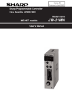
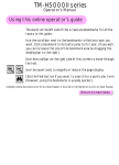
Sharp Programmable Controller
Board PC J-board
Z-500 series
Model name
CPU Board 1 : Z-511J
CPU Board with communication function
User's Manual / Hardware version
CAUTION
5 VDC is required to power the Z-511J. Be careful not to apply any other DC or AC voltage
such as 24 VDC and 100 VDC. Otherwise, the Z-511J will be destroyed.
Sharp Programmable Controller
Board PC J-board
Model name
Z-511J
CPU Board 1:Z-511J
CPU board with communication function
COMM1
User's Manual / Hardware version
COMM2
COMM2
(RS422A)
Data link port
5 VDC power source
FG
0V
5V
Power supply (5 VDC input)
5.0 to 5.2 VDC
Thank you for purchasing a J-board Z500 series programmable controller. This manual (User’s Manual:
Hardware Version) mostly describes hardware details, including specifications and installation procedures
of the J-board.
Before using the J-board, read this manual together with the "JW30H Programming Manual, Ladder Instruction Version," that describes software details such as the available instructions, the "JW-21CM User's Manual"
and the "Maintenance Manual for Interface Modules" that describe communication functions.
In addition, learn the handling methods for other I/O and communication boards by reading each "User's
Manual."
- Should you have any questions and inquiries please feel free to contact our dealer’s shop.
- The whole or partial photocopy of this booklet is prohibited.
- Contents of this booklet may be revised for improvement without notice.
Safety Precautions
Read this user's manual and attached documents carefully before installation, operation, maintenance and
checking in order to use the J-board correctly. Understand all of the J-board knowledge, safety information,
and cautions before starting to use. In this user's manual, safety precautions are ranked into "Danger" and
"Caution" as follows.
Danger
: Wrong handling may possibly lead to death or heavy injury.
Caution : Wrong handling may possibly lead to medium, light injury, or loss on properties.
Even in the case of
Caution , a serious result may be experienced depending on the circumstances.
Anyway, important points are mentioned. Be sure to observe them strictly.
The picture signs of prohibit and compel are explained below.
: It means a don’t. For example, prohibition of disassembly is indicated as (
: It means a must. For example, obligation of grounding is indicated as (
).
).
1) Installation
Caution
• Use in the environments specified in the catalog and user's manual.
Electric shock, fire or malfunction may be caused when used in the environments of high
temperature, high humidity, dusty or corrosive atmosphere, vibration or impact.
• Install according to the instruction manual and user's manual.
Wrong installation may cause drop, trouble or malfunction.
• Never admit wire chips or foreign matter.
Or fire, trouble or malfunction may be caused.
2) Wiring
Compel
• Be sure to ground.
Unless grounded, electric shock or malfunction may be caused.
Caution
• Connect the rated power source.
Connection of a wrong power source may cause a fire.
• Wiring should be done by a qualified electrician.
Wrong wiring may lead to fire, trouble or electric shock.
3) Use
Danger
• Don’t touch the terminal while the power is being supply or you may have on electric shock.
• Assemble the emergency stop circuit and interlock circuit outside of the J-board and connect
to the halt output of the J-board. Otherwise the machine breakdown or accident may be
caused by the trouble of the J-board.
Caution
• "Run" or "stop" during operation should be done with particular care by confirming safety.
Mis-operation may lead to damage or accident of the machine.
• Turn ON the power source in the specified sequence. Turn ON with wrong sequence may
lead to machine breakdown or accident.
4) Maintenance
Danger
• The Z-511J controller contains a lithium battery. Do not expose the Z-511J directly to flames
as the battery may explode and seriously injure people nearby.
Prohibit
• Don’t disassemble or modify.
Or fire, trouble or malfunction may be caused.
Caution
• Turn OFF the power before attaching or removing the board, attaching the I/O connector,
modifying each type of setting switch.
Or electric shock, malfunction or trouble may be caused.
Table of Contents
page
1.
2.
3.
4.
5.
6.
7.
8.
9.
10.
Outline ............................................................................................................................................. 1
Special precautions ....................................................................................................................... 1
Board configuration ....................................................................................................................... 3
System configuration .................................................................................................................... 4
Specifications of Z-511J ................................................................................................................ 9
5-1. General specifications ........................................................................................................... 9
5-2. Performance specifications (CU section) ............................................................................. 9
5-3. Performance specifications (CM section: data link port) ................................................. 10
5-4. Name and description of each part ...................................................................................... 11
5-5. Data memory ......................................................................................................................... 15
5-6. System memory .................................................................................................................... 15
Current consumption of each board .......................................................................................... 16
Board size ..................................................................................................................................... 17
Assemble/fixing ........................................................................................................................... 18
8-1. Assemble ............................................................................................................................... 18
8-2. Fixing ..................................................................................................................................... 19
8-3. Specialized fixing bracket .................................................................................................... 20
The horizontal extension connector .......................................................................................... 21
Allocation of I/O relay .................................................................................................................. 23
10-1. Basic description ................................................................................................................ 23
10-2. I/O relay allocation .............................................................................................................. 23
10-3. Example for I/O relay allocation ........................................................................................ 24
11. ROM operation ............................................................................................................................. 27
12. Upstream communication port ................................................................................................... 28
13. Data link port ................................................................................................................................ 39
14. Items the user must supply ........................................................................................................ 41
1. Outline
Programable controller "J-board: Z-500 series," hereafter referred to as "the J-board," realized both
compactness and low cost by employing a board type structure together with various communication
functions which only larger class models have. It is a programmable controller for middle and small
scale control systems, suitable for integrating into equipment and providing local control of distributed
control systems.
2. Special precautions
Precautions for installation
Never install the J-board in the following locations.
· Where proximate to any heat generating object, or ambient temperature exceeding 0 to 55˚C range
(at storage -20 to 70˚C).
· Where temperature rapidly changes and gives dew condensation.
· Where there is corrosive or flammable gas.
· Where it directly receives vibration or shocks.
· Where exposed to dust, iron powder, or salty atmosphere.
(In conditions where the printed circuit boards may be directly affected by these causes, make sure
to provide an appropriate external case to cover the J-board.)
· Where it is proximate to high voltage equipment, driving power tools, large open/close surge generating devices, and their wirings.
Precautions at use
· Construct an emergency stop circuit externally to prevent damage to machines and personnel and
connect with a halt output for the J-board.
· As the J-board is board structure and it’s electronic parts are exposed, be careful when handling.
1 Before you touch the board directly, be sure to eliminate static electricity in your body.
2 Do not touch directly with dirty hands such as stacked oil etc.
3 Do not put the board alone directly on conductive objects such as metallic boards.
(When the board is put directly on conductive objects such as metallic boards, battery terminals
of the board may be shorted and the back-up memory may be lost.)
4 Be careful not to apply excessive force to each switch, connector, terminal block of the J-board.
· Make sure to turn OFF the power before connecting the board, installing the I/O connector, changing
a switch setting, or mounting a ROM for ROM operation.
Precautions for grounding
Provide class-3 grounding independently for FG terminal of the J-board (on a terminal block of the
CPU board). Do not use with a high voltage ground line in common.
Precautions for wiring work
· Required voltage of the Z-511J is 5 VDC. Be careful not to exceed voltage or reverse the polarity.
(Overvoltage and reversed polarity may damage the internal circuits.)
· A 5 VDC power supply for the Z-511J should be kept away from sources of electrical noise such as
separate from a power supply for loads.
· Do not run I/O lines and communication lines parallel or proximate with power lines and high voltage
lines. Do not run noise generating lines such as power lines, high voltage lines, and I/O lines proximate above the printerd circuit board of the J-board.
· Some I/O boards are equipped with a fuse for output circuit protection. If the fuse is blown by a short
circuit, change whole of the I/O board after repairing the external cause.
* The integrated fuse in the I/O board is to prevent heating by overcurrent and burn out of internal
circuit at shorted loads, and does not protect output elements.
-1-
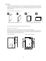
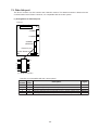
Precautions for installation
Basically use the fixing bracket exclusive for installing the J-board and apply any of the recommended
installation conditions shown below (1, 2, 3, or 4 of figures below). If you intend to install the J-board
without using the fixing bracket, install it with sufficient holding strength. Install J-board in well ventilated conditions.
<Recommendation fixing conditions>
1
2
When fixing bracket A
(Z-341J) is used
3
4
When fixing bracket B
(Z-342J) is used
In case of plane installation shown below, the J-board is not given sufficient ventilation. Therefore,
provide enough space above J-board to prevent temperature rise exceeding 55˚C.
Not good ventilation
Note: The fixing bracket B (Z-342J) cannot be used with the Z-325J.
Precautions for memory back up
The Z-511J contains a memory backup battery. Do not store the Z-511J in high temperatures or at
high humidity. Storing it at high temperatures will greatly reduce the battery life.
Do not put any object directly on the top of the Z-511J.
-2-
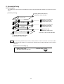
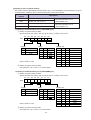
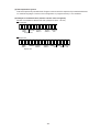
3. Board configuration
Z-511J: CPU board
Connector
for stacking
Horizontal extension connector
Mounted parts
25 mm
COMM1
COMM2
COMM2
(RS422A)
Accessories
Standoff used to attach the PC board to
the fixing bracket (15 mm): 4 pieces
Standoff
Screw (Semus M3 x 6 mm): 4 pieces
Screw
Data link port
5 VDC Power source
-3-
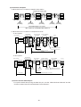
4. System configuration
<Basic system>
Stacking structure
Up to 7 I/O boards can be installed (including horizontal
arranged modules), and up to 2 optional boards can be
installed. (However, a total of 8 boards can be installed
including the CPU board.)
I/O board
Optional board
Z-511J
COMM1
COMM2
PG port, upstream communication port
PG port, upstream communication port.
(RS232C or RS422A)
Support
tool
Upstream communication port (RS422A) 5-pin connector
Data link port (DL1, DL9, CL, or M-net can be used),
5-pin connector
5V DC in
Proprietary cable (JW-203EC, JW-207EC)
I/O board
I/O board
(Z-325J)
*If Z-325J is used as I/O board, horizontal
installation is possible.
-4-
<DL1 data link system>
No. of connected stations: Max. 16 stations
Total extension length: 1 km
Transfer rate: 153.6 kbps
No. of link points: Max. 64 bytes.
* When JW-21CM or J-board are used as the master station, the number of link points
per station is restricted by the number of connected stations.
J-board
I/O board
CPU board
Z-511J
J-board
Communication
Z-332J board I/O board
Z-331J
CPU board
Z-311J
Z-312J
JW20, JW20H
JW30H
JW50/70/100(H)
JW-21CM
JW-10CM
[DL1 data link communication system]
The DL1 data link is a communication system used to send and receive data between the master
station and a slave station, and between slave stations, as shown in the figure below.
Master station
(00 station)
Slave station 01
Own station
sending data
Slave station 02
Slave station 03
Receiving data
from master station
Receiving data
from master station
Receiving data
from master station
Receiving data from
slave station 01
Own station
sending data
Receiving data from
slave station 01
Receiving data from
slave station 01
Receiving data from
slave station 02
Receiving data from
slave station 02
Own station
sending data
Receiving data from
slave station 02
Receiving data from
slave station 03
Receiving data from
slave station 03
Receiving data from
slave station 03
Own station
sending data
-5-
<DL9 data link system>
No. of connected stations: Max. 16 stations
Total extension length: 1 km
Transfer rate: 153.6 kbps
No. of link points: Max. 512 bytes.
* When JW-21CM or J-board are used as the master station, the number of link points
per station is restricted by the number of connected stations.
J-board
I/O board
CPU board
Z-511J
J-board
Communication
Z-332J board I/O board
Z-331J
CPU board
Z-311J
Z-312J
JW20, JW20H
JW30H
JW50/70/100(H)
JW-21CM
JW-10CM
[DL9 data link communication system]
The DL9 data link is a communication system used to send and receive data between the master station
and a slave station as shown in the figure below.
* Direct communication between slave stations is not possible.
Master station (00 station)
Slave station 01
Sending data to
slave station 01
Receiving data
from master station
Receiving data from
slave station 01
Sending data to
master station
Slave station 02
Sending data to
slave station 02
Receiving data
from master station
Receiving data from
slave station 02
Sending data to
master station
Slave station 03
Sending data to
slave station 03
Receiving data
from master station
Receiving data from
slave station 03
Sending data to
master station
-6-
<M-net system>
No. of connected stations: Max. 8 stations
Total extension length: 1 km
Transfer rate: 19.2 kbps/38.4 kbps
No. of link points: Max. 64 bytes.
J-board
I/O board
CPU board
Z-511J
J-board
JW20,
JW50/70/
JW20H
100(H)
Communication
JW30H
Z-332J board I/O board
Z-331J
CPU board
Z-311J
Z-312J
JW-21CM
JW-10CM
Others, M-net
specification
equipment
[M-net communication system]
The M-net is a communication system used to send and receive data between the master station and a
slave station as shown in the figure below.
* Direct communication between slave stations is not possible.
Master station (00 station)
Slave station 01
Sending data to
slave station 01
Receiving data
from master station
Receiving data from
slave station 01
Sending data to
master station
Slave station 02
Sending data to
slave station 02
Receiving data
from master station
Receiving data from
slave station 02
Sending data to
master station
Slave station 03
Sending data to
slave station 03
Receiving data
from master station
Receiving data from
slave station 03
Sending data to
master station
* The M-net is a communication system used to create a data link between a programmable controller
and other equipment. It is a communication conforming to the "Standard for the interface between
modules."
-7-
<Computer link (CL) system>
No. of connected stations: Max. 32 stations
Total extension length: 1 km
Transfer rate: 300 to 19200 bps
Host device
Personal computer,
monitor, etc
J-board
I/O board
CPU board
Z-511J
J-board
Communication
Z-332J board I/O board
Z-331J
CPU board
Z-311J
Z-312J
JW20, JW20H
JW30H
JW50/70/100(H)
JW-21CM
JW-10CM
[Computer link communication system]
The computer link is a communication method in which the J-board responds to commands from a host
personal computer and display unit, as shown in the figure below.
J-board or JW-PLC
(station No. 01)
Host
Command
Personal computer,
monitor, etc.
Response
J-board or JW-PLC
(station No. 02)
Command
Response
J-board or JW-PLC
(station No. 03)
Command
Response
-8-
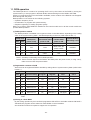
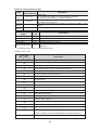
5. Specifications of Z-511J
5-1. General specifications
Item
Specifications
Allowable power voltage
5 VDC (5.0 to 5.2V)
The 5V power supply must be able to handle the total of the current
consumption from all of the boards. MAX. 2.7A
Ambient operation
temperature / humidity
0 to 55oC / 35 to 90%RH (without dewing)
Storage temperature /
humidity
-20 to 70oC / 35 to 90%RH (without dewing)
Vibration resistance
JIS-C-0911 or equivalent, double amplitude : 0.15 mm (10 to 55Hz),1G
(55 to 150Hz), 2 hours each in X, Y, and Z directions
Shock resistance
JIS-C-0912 or equivalent, 10G, 3 times each in X, Y, Z directions
Installation
Any of 3 directions
Grounding
Class-3 grounding
5V current consumption
Approx. 700 mA
Weight
Approx. 400 g
Board size
115 mm x 190 mm
External interface
Calculation port/memory section
5-2. Performance specifications (CU section)
Item
Calculation method
Processing speed
Basic instruction
TMR, CNT
Application
instruction
Numbers of instruction
Program size
ROM operation
Memory back-up
No. of control I/O points
Timer, counter
Data memory
Connectable I/O board
Clock feature
Host communication port
Data link port
Support tool
PG port
Applicable model
Model setting
Connection cable
Specifications
Cyclic calculation and interrupt dealing system
Equivalent to JW30HN
0.038 µseconds. (STR, AND, OR, and others), 0.076 µseconds (OUT)
Few µsecconds on average
Few µ. to few tens µsecconds on average
Basic instruction : 20, application instruction: 113
15.5 K words (equivalent to the JW32CHU1)
ROM operation with an internal flash ROM
Back up by an integrated lithium primary side battery
1024 points (equivalent to the JW32CUH1)
1024 points in total
30720 relay and other points. File register: 80 K bytes
Up to 8 modules, including this module, can be installed.
Yes
Use PG/COMM1 port or PG/COMM2 port.
Communication standard: RS232C/RS422A (Only PG/COMM2 port can
be used for RS232C)
With an RS422A connection, 1: N connection is available. D-sub 15-pin
or proprietary connector. The port complies with the Sharp computer link
protocol (Max. 115.2 K bit/s)
RS485 (proprietary connector)
The DL1 data link, DL9 data link, M-net, or computer link can be
connected.
2 D-sub 15-pin connectors. Shared with the communication port to
connect to host computers.
Hand-held programmer (JW-13PG)
Application program JW92SP (for PC98), JW50SP (for IBM PC)
JW-32CUH1 15.5K
Exclusive cable: JW-22KC (2 m) or JW-24KC (4 m)
-9-
5-3. Performance specifications (CM section: data link port)
Item
Specifications
DL1 data link
Communication
standard
EIA RS-485 or equivalent
SW5 = 2
Transmission rate
153.6 k bps
JIS X-5104.
Transmission format Conforms to the frame organization of the High level Data Link Control (HDLC) protocol.
Data check: CRC
Communication line
No. of connected
stations
No. of link bytes
Link area
Shielded twisted pair cable. Cable total length: Max. 1 km (party line connection)
Max. 16 stations (1 master station + 15 slave stations)
Max. 64 bytes *When the master station is a Z-551J, Z-313J, Z-331J, Z-332J or JW-21CM, the
following limitations apply.
In case of 1 slave station: 32 bytes per station
In case of 2 to 3 stations: 16 bytes per station
In case of 4 to 7 stations: 8 bytes per station
In case of 8 to 15 stations: 4 bytes per station
Set using SW8 (module No. SW)
DL9 data link
Communication
standard
EIA RS-485 or equivalent
SW5 = 3
Transmission rate
153.6 k bps
Transmission format
JIS X-5104.
Conforms to the frame organization of the High level Data Link Control (HDLC) protocol.
Data check: CRC
Communication line
Shielded twisted pair cable. Cable total length: Max. 1 km (party line connection)
No. of connected
stations
Max. 16 stations (1 master station + 15 slave stations)
No. of link bytes
Max. 512 bytes
When the master station is a Z-313J, Z-331J, Z-332J or JW-21CM, the following limitations apply.
In case of 1 to 2 stations: Max. 128 bytes per station
In case of 3 to 4 stations: Max. 64 bytes per station
In case of 5 to 8 stations: Max. 32 bytes per station
In case of 9 to 15 stations: Max. 16 bytes per station
Link area
Assign using SW3 (module No. switch)
M-net
Communication
standard
EIA RS-485 or equivalent
SW5 = 7
Transmission rate
19.2 k bps/38.4 k bps
Transmission format
M-net (interface between modules) specifications or equivalent
Start (1) + data (7) + even parity (1) + stop (1)
Communication line
Shielded twisted pair cable. Cable total length: Max. 1 km (party line connection)
No. of connected
stations
Max. 8 stations (1 master station + 7 slave stations)
No. of link bytes
Link area
Max. 64 bytes
Set by the parameter (parameter address is determined by SW8)
Computer link
Communication
standard
EIA RS-485 or equivalent
SW5 = 4
Transmission rate
300, 600, 1200, 2400, 4800, 9600, 19200 k bps
Start-stop synchronization
Transmission format Start (1) + data (7) + parity (1) + stop (2).
Used character: ASCII alphanumeric character
Communication line
Shielded twisted pair cable. Cable total length: Max. 1km (party line connection)
The wiring system is 2-wire system. (4-wire system is no available.)
No. of connected
stations
Maximum of 32 stations (one host station + 31 slave stations)
[Allocation of Z-511J address]
Address(8)
コ. 0000
コ. 0001
コ. 0002
コ. 0003
コ. 0004
コ. 0005
コ. 0006
コ. 0007
Allocation
No. of bytes occupied
CM section (dummy)
Vacant
8 bytes
Vacant
Vacant
-10-
5-4. Name and description of each part (Z-511J)
LEDs on the CPU board
RUN (green)
A connector for extended horizontal layouts
COMM1 (white)
CN11
SW13
CN10
protect
COMM2 (white)
FAULT (red)
[ Protect switch]
CN8
COMM1
Connector for the PG port or for
the upstream communication port.
(D-sub 15-pin, female)
SWA
CN9
COMM2
Connector for the PG port or for
the upstream communication
port. RS232C or RS422A.
(D-sub 15-pin, female)
SW10
SW1
SW3
CN5
SW7
SW9
Connector for the upstream
communication port. Shared use
with COMM2. RS422A. (Molex:
5278-05AG)
SW6
SW8 SW2 SW4 SW5
CN4
Data link port. DL1, DL9, CL, or Mnet can be used. RS422A (Molex:
5278-05AG)
Backup battery
FG
Power connector: 5 VDC input
(Molex: SD-53376-0310)
CN3
FG 0V 5V
FT (red)
ER (red)
T (green)
RS (green)
RD (green)
SD (green)
CM (green)
Connect to a ground
Data link port LEDs
Table of applicable connectors
Connector
Data transfer
Connector name
Applicable connector
number
standard
CN5
Upstream communication port
RS422A
Molex: 5265-N, 2578G
CN4
Data link port
RS422A
Molex: 5265-N, 2578G
CN3
5 VDC power
Molex: 51102-0500, 50351-8100
-11-
LEDs on the CPU board
J-board status
RUN
FAULT
Operation mode
Stop mode
Error
Goes ON
Blinks
Goes OFF
Goes OFF
Goes OFF
Goes ON
CN5
FG
TXDA
TXDB
RXDA
RXDB
CN4
FG
L1
L2
L3
L4
CN3
FG 0V 5V
CN5: CPU section upstream communication port (5-pin)
Signal name
FG
TxDA
TxDB
RxDA
RxDB
Description
Frame ground (connect to the shield)
Sending data (+)
RS422A upstream
Sending data (-)
Receiving data (+) communication port
Receiving data (-)
CN4: Data link port (5-pin)
Signal name
Description
FG
Frame ground (connect to the shield)
L1
Sending data, receiving data (+)
L2
Sending data, receiving data (-) RS422A upstream
communication port
L3
Receiving data (+)
L4
Receiving data (-)
CN3: Power connector
Signal name
Description
FG
Frame ground
0V
Power input (0V)
5V
Power input (5V)
-12-
Description of the indicator lamps (Z-511J)
CU section
LED name
RUN (green)
FAULT (red)
LED name
Display condition
Operation mode
Goes ON
Goes OFF
Stop mode
Blinks
Goes OFF
When an error occurs
Goes OFF
Goes ON
Display condition
COMM1
(orange)
Monitor data transmission and reception of a peripheral
device or host computer connected to COMM1.
COMM2
(orange)
Monitor data transmission and reception of a peripheral
device or host computer connected to COMM2.
CM section
1) On a DL1 data link, DL9 data link, or computer link
LED name
Display condition
CM (green) Goes ON during link operation (communication)
SD (green) Goes ON while sending data
RD (green) Goes ON while receiving data
RS (green) Goes ON during link operation (request to send data)
Goes ON during a test (Used for inspection by the
T (green)
manufacturer)
ER (red)
Goes ON when a SW setting error occurs
FT (red)
Goes ON when the WDT time out
2) On an M net
LED name
Display condition
CM (green) Goes ON during link operation (communication)
SD (green) Goes ON while sending data
RD (green) Goes ON while receiving data
RS (green) Goes ON during link operation (request to send data)
Goes ON during a test (Used for inspection by the
T (green)
manufacturer)
ER (red)
Goes ON when a communication error occurs.
FT (red)
Goes ON by when the WDT times out
Recovery
Check switch settings.
Replace the board.
Replace the board.
Recovery
Check switch settings,
parameter settings,
disconnected
communication cable,
replace the board.
Replace the board.
Note
The CM section does not have LEDs for displaying error codes. Monitor the system memory (#170 and up)
and check the error details.
* To learn about error details and troubleshooting, see the "JW-21CM User's Manual," "Maintenance Manual
for Interface Modules," and the "JW-23LM User's Manual."
-13-
Description of each switch
Switches in the CU section
Switch
Switch details
no.
Default setting
SWA-1
ON
Slot assignment switch.
Specifies whether it is the first or last half in the same rack number.
SWA-2
ON
Recovery switch. Turn ON the power while pressing this switch to
SW7
recover from an error condition. such as a memory error. The details are
maintained in memory. To clear the memory, take other steps.
SW1-1
OFF
Rack number switch.
SW1-2
OFF
Assign a rack address.
SW1-3
OFF
SW13
OFF
Prohibit (ON) or allow (OFF) writing the program and system memories.
Switches in the CM section
Switch
No.
Switch details
SW9-1
Default
setting
OFF
SW9-2
OFF
DL1 data link
DL9 data link
M-net
Computer link
OFF
OFF
OFF
OFF
OFF: 2-wire system
ON: 4-wire system
OFF
OFF
Specify the total
number of link
bytes (set only
when used as a
master station)
Communication
mode when an
error occurs.
SW10-1
OFF
OFF
SW10-2
OFF
OFF
SW6-1
OFF
Not used
Not used
Not used
SW6-2
OFF
Termination
resistance
Termination
resistance
Termination
resistance
Upper digit of
station number
Lower digit of
station number
Upper digit of
station number
Lower digit of
station number
Upper digit of
station number
Lower digit of
station number
Module No.
switch
SW8
0
SW2
0
SW3
0
SW4
0
SW5
0
Module No. switch Module No. switch
Number of slave
stations (only
when used as a
master station)
2
Number of slave
stations (only when
used as a master
station)
3
-14-
OFF
OFF
Parity
OFF: Odd
ON: Even
Termination
resistance (4-wire
system)
Termination
resistance (2-wire
system)
Upper digit of station
number
Lower digit of station
number
Module No. switch
Data transfer
speed
Data transfer speed
7
4
5-5. Data memory (Z-511J)
See pages 2-1 to 2-3 in the "JW30H Programming Manual, Ladder Instruction Version." (The details are
identical to the JW32CUH1)
5-6. System memory (Z-511J)
See pages 3-1 to 3-2 and 5-1 to 5-17 in the "JW30H Programming Manual, Ladder Instruction Version."
(The details are identical to the JW32CUH1)
-15-
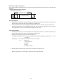
6. Current consumption of each board
The current requirement of the Z-511J is the total current consumption of all the boards and support tools
connected to it.
Current consumption of each board
Model name
Z-511J: CPU board
Current consumption
700 mA
111 mA (when all of the output points are ON). When
Z-321J: 32 point I/O board
"N" number of points are ON = 10 + 6.3 N1 (N1:
Number of points whose output is ON)
212 mA (when all of the output points are ON). When
Z-322J: 64 point I/O board
"N" number of points are ON = 10 + 6.3 N1 (N1:
Number of points whose output is ON)
126 mA (when all of the output points are ON). When
"N" number of points are ON = 15 + 2.5N1 + 12N2 (N1:
Z-323J: 30 point I/O board
Number of points whose TR output is currently turned
ON. N2 = Number of points whose triac output is
currently turned ON)
38 mA (when all of the output points are ON). When "N"
Z-324J: 28 point I/O board
number of points are ON = 10 + 2.3N1 (N1: Number of
points whose output is ON)
267 mA (when all of the output points are ON). When
Z-325J: 64 point I/O board 2
"N" number of points are ON = 15 + 6.3N1 (N1: Number
of points whose output is ON)
Z-331J: Communication board 1 (LM+CM) 170 mA
Z-332J: Communication board 2(CM)
100 mA
Z-333J: Communication board 3 (LM)
80 mA
Z-334J: ME-NET board
330 mA
Z-335J: Satellite net board
280 mA
Z-351J: Analog input board
60 mA
Z-352J: Analog output board
100 mA
Z-353J: Pulse output board
120 mA
Support tool (JW-2PG, JW-13PG)
150 mA
-16-
7. Board size
Printed circuit board size
100 mm
5 mm
25 mm
* 5 mm
D
170 mm
CPU board *
D2
Standoff hole
4-f4
W
D2
I/O board or
communication
board
D2
D2
15 mm
In case of fixing bracket A
5 mm
* CPU board should be installed on the top.
H
* 15 mm for Z-511J and Z-325J
Board size (Fixing bracket size is excluded.)
Type
Z-511J: CPU board
Z-321J: 32 point I/O board
Z-322J: 64 point I/O board
Z-323J: 30 point I/O board
Z-324J: 28 point I/O board
Z-325J: 64 point I/O board 2
Z-331J: Communication board 1 (LM+CM)
Z-332J: Communication board 2 (CM)
Z-333J: Communication board 3 (LM)
Z-334J: ME-NET board
Z-335J: Satellite net board
Z-351J: Analog input board
Z-352J: Analog output board
Z-353J: Pulse output board
Z-341J: Fixing bracket A
Z-342J: Fixing bracket B
H
115 mm
110 mm
110 mm
117.5 mm
115 mm
115 mm
117.5 mm
117.5 mm
117.5 mm
117.5 mm
117.5 mm
117.5 mm
117.5 mm
117.5 mm
W
190 mm
180 mm
180 mm
180 mm
180 mm
190 mm
180 mm
180 mm
180 mm
180 mm
180 mm
180 mm
180 mm
180 mm
D
25.0 mm (D1)
16.6 mm (D2)
16.6 mm (D2)
21.6 mm (D2)
21.6 mm (D2)
16.6 mm (D2)
16.6 mm (D2)
16.6 mm (D2)
16.6 mm (D2)
21.6 mm (D2)
21.6 mm (D2)
21.6 mm (D2)
21.6 mm (D2)
16.6 mm (D2)
See "8-3. Specialized fixing bracket"
Weight *
Approx. 230 g
Approx. 125 g
Approx. 135 g
Approx. 180 g
Approx. 210 g
Approx. 170 g
Approx. 180 g
Approx. 180 g
Approx. 180 g
Approx. 250 g
Approx. 250 g
Approx. 220 g
Approx. 210 g
Approx. 200 g
Approx. 220 g
Approx. 290 g
* Including standoffs and screws
Example for measurement D
Board composition
CPU board + one I/O board + fixing bracket A
CPU board + two I/O boards + fixing bracket A
CPU board + three I/O boards + fixing bracket A
CPU board + four I/O boards + fixing bracket A
-17-
Measurement D
When the board
When the board
(D2=16.6 mm) is/are
(D2=21.6 mm) is/are
used.
used.
56.6 mm
61.6 mm
73.2 mm
83.2 mm
89.8 mm
104.8 mm
105.2 mm
126.4 mm
8. Assemble/fixing
8-1. Assemble
For building up of the J-board, assemble the boards using the attached standoffs and screws as shown
below.
[Assembly drawing]
Screw (Semus M3 X 6 mm)
Attached to each of board.
1
CN
N1
C
CPU board
Standoff: 15 mm/20 mm
Attached to I/O board,
communication board
I/O board
(Communication board)
Standoff: 15 mm/20 mm
Attached to I/O board,
communication board
1
CN
I/O board
(Communication board)
Standoff: 10 mm
Attached to CPU board
Fixing bracket A
* The Z-511J has 15 mm standoffs.
Screw (Semuth M3 X 6 mm)
Attached to each of board.
Notes For connecting between the boards, match position of each connection connector (CN1)
and secure their inserts. For removal, be careful not to forcibly pull them in an incorrect
direction.
[Required tools for building up]
- Phillips screw driver
- Box (hex.) driver: for 5.5 mm
-18-
Standoff shape
5.5 mm
8-2. Fixing
Basically use the fixing bracket exclusive for installing the J-board and apply all of the recommended
installation conditions shown below (1, 2, 3 or 4 of figures below). If you intend to install J-board
without using the fixing bracket, install it with sufficient holding strength. Install the J-board in well
ventilated condition.
<Our recommendation fixing conditions>
1
2
3
When fixing bracket A (Z-341J) is used
4
When fixing bracket B (Z-342J) is used
Note: The fixing bracket B (Z-342J) cannot be used with the Z-325J.
<Spare space for installation>
For spare space for connector wiring work of each board, see the figures below.
(Spare space dimensions nominated below are not considered for attachment and detachment of
wires after installation. Required spare space may vary with wiring method and used cable size so
confirm final required space at actual wiring work.)
Z-511J: CPU board
Z-325J: 64-point I/O board 2
90 mm
15 mm
COMM1
25 mm
25 mm
COMM2
COMM2
(RS422A)
Upstream
communication
5 VDC Power source
25 mm
-19-
8-3. Specialized fixing bracket
Fixing bracket A: Z-341J (Plane fixing type)
[Bracket size]
[Fixing halls drilling dimensions]
4-φ5 (Fixing hall)
0.5 mm
1.2 mm (t)
116 mm
4.5 mm
(Board)
10.7 mm
205 mm
205 mm
196 mm
Fixing bracket
outside diameter
10.7 mm
4.5 mm
Fixing screw: M4
8 mm
100 mm
8 mm
Fixing bracket B: Z-342J (Vertical fixing type)
[Bracket size]
50 mm
Fixing screw: M4
117.2 mm
(Board)
1.2 mm (t)
[Fixing halls drilling dimensions]
50 mm
4.5 mm
4-φ5 (Fixing hall)
205 mm
196 mm
Fixing bracket outside diameter
4.5 mm
30 mm
10 mm
10 mm
Fixing screw should be prepared by user.
-20-
9. The horizontal extension connector
The Z-511J and Z-325J are equipped with a connector for horizontal boards (CN11) in addition to
stacking connector (CN10.)
The horizontal arrangement shown below is available.
Specialized cable: JW-203EC (30 cm) or JW-207EC (70 cm)
24VDC (4P terminal block)
Z-325J
Z-511J
OUT
CN-H
(10P)
CN-A
(14P)
OUT
CN-G
(10P)
CN-B
(14P)
IN
OUT
CN-F
(10P)
CN-C
(14P)
IN
COMM1
IN
COMM2
COMM2
(RS422A)
Upstream
communication
5 VDC Power source
OUT
CN-E
(10P)
OUT
CN-D
(10P)
<Installation limit>
1 Several J-boards can be installed under the Z-511J as the stacked installation.
2 To connect boards horizontally, an I/O board with a horizontal extension connector should be at the
top.
* Only the Z-325J has the horizontal extension connector.
3 The horizontal I/O board cannot be connected the communication board.
4 Do not set SW1 (RACK NO.) to "0" on the horizontal I/O board.
(Make sure to set 1 to 3.)
5 Four input/output boards and three communication board can be connected to the Z-511J, including when arranged horizontally.
6 Be sure to use the specialized cables listed below for the horizontal extension cable.
Model name
JW-203EC
JW-207EC
Cable length
30 cm
70 cm
-21-
<Example of a horizontal arrangement>
Specialized cable: JW-203EC (30 cm) or JW-207EC (70 cm)
Z-325J
I/O board
I/O board
Z-325J
Communication
board
Z-325J
Z-344J
Z-511J
CN
Dimension D
D
16.6 mm
Z-325J
16.6 mm
Z-325J
16.6 mm
15 mm
Z-325J
25 mm *
D
21.6 mm
Z-511J
Z-334J
15 mm
* Including table connector depth, when horizontal arrangement connector is connected.
Board composition
Z-325J
Z-325J + Z-325J
Z-325J + Z-325J + Z-325J
Measurement D
31.6 mm
48.2 mm
64.8 mm
Board composition
Z-511J
Z-511J + Z-334J
-22-
Measurement D
35 mm
56.6 mm
10. Allocation of I/O relay
10-1. Basic description
The I/O relay addresses are assigned using SW1 and SW2 (SWA) on each board, as shown in the table
below.
SW1 (RACK NO.) settings
The rack numbers are assigned as shown in the table below.
SW1 (RACK NO.) settings
1
OFF
1 2 3
2
OFF
3
OFF
ON
1
1 2 3
OFF
2
OFF
3
OFF
1
1 2 3
ON
2
OFF
3
OFF
1
1 2 3
OFF
2
ON
3
Rack number
Rack. NO = 0
Rack. NO = 1
Rack. NO = 2
Rack. NO = 3
SW2 (SWA) settings
1: Assigns the first half or last half of a rack. (ON = first half, and OFF = last half.)
If you use two communication boards, set the second communication board to "OFF."
2: Set the number of bytes used. (ON = 8 bytes, and OFF = 4 bytes.)
Normally, this switch is set to "ON."
2
2
2
2
SW2 settings
1
1
2
1
1
2
1
1
2
1
1
2
Details
ON
ON
ON
OFF
OFF
ON
OFF
OFF
First half
8 bytes occupation *
First half
4 bytes occupation **
Last half
8 bytes occupation *
Last half
4 bytes occupation **
* 10 bytes occupation in the case of Z-325J
** 6 bytes occupation in the case of Z-325J
Note 1. Be careful not to set the same number for more than one board with SW1 (RACK No.) and SW2.
When multiple boards are allocated on the same I/O, J-board malfunctions.
Note 2. When more than one point is turned ON with SW1 (RACK No.), "I/O verify error: Error code 60"
occurs.
10-2. I/O relay allocation of Z-511J
Type
CM
Dummy
CM
Dummy
Vacant
Dummy
Vacant
Dummy
Vacant
Dummy
Vacant
Dummy
Vacant
Dummy
Address (OTC)
コ.N
コ.N+1
コ.N+2
コ.N+3
コ.N+4
コ.N+5
コ.N+6
Vacant
コ.N+7
Dummy
-23-
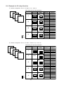
10-3. Example for I/O relay allocation
1 Vertical arrangement: Z-511J + Z-325J x n (n = max. 3)
SW setting and I/O relay allocation
Z-325J
Installation
SW1
(RACK NO)
1
1 2 3
Z-325J
SWA
Z-325J
4
Z-511J
3
SW2
(SWA)
2
1 2
SW2
1
1 2 3
2
1 2
SW2
1 2 3
3
1 2
SW2
1 2 3
4
1 2
ON
OFF
I/O relay
address
コ. 000,001
コ. 002,003
コ. 004,005
コ. 006,007
コ. 010,011
コ. 012,013
コ. 014,015
コ. 016,017
コ. 020,021
コ. 022,023
コ. 024,025
コ. 026,027
コ. 030,031
コ. 032,033
コ. 034,035
コ. 036,037
コ. 040,041
コ. 042,043
コ. 044,045
Installed
address
R = 0, S = 0
R = 0, S = 1
R = 0, S = 2
R = 0, S = 3
R = 1, S = 0
R = 1, S = 0
R = 1, S = 1
R = 1, S = 2
R = 1, S = 3
R = 2, S = 0
R = 2, S = 0
R = 2, S = 1
R = 2, S = 2
R = 2, S = 3
R = 3, S = 0
R = 3, S = 0
R = 3, S = 1
R = 3, S = 2
R = 3, S = 3
I/O relay
address
コ. 000.001
コ. 002,003
コ. 004,005
コ. 006,007
コ. 010,011
コ. 012,013
コ. 014,015
コ. 016,017
コ. 020,021
コ. 022,023
コ. 024,025
コ. 026,027
コ. 030,031
コ. 032,033
コ. 034,035
コ. 036,037
コ. 040,041
コ. 042,043
コ. 044,045
コ. 046,047
コ. 050,051
コ. 052,053
コ. 054,055
Installed
address
R = 0, S = 0
R = 0, S = 1
R = 0, S = 2
R = 0, S = 3
R = 0, S = 4
R = 0, S = 5
R = 0, S = 6
R = 0, S = 7
R = 1, S = 0
R = 1, S = 0
R = 1, S = 1
R = 1, S = 2
R = 1, S = 3
R = 2, S = 0
R = 2, S = 0
R = 2, S = 1
R = 2, S = 2
R = 2, S = 3
R = 3, S = 0
R = 3, S = 0
R = 3, S = 1
R = 3, S = 2
R = 3, S = 3
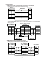
2 Vertical arrangement: Z-511J + Z-334J + Z-325J x n (n = max. 3)
SW setting and I/O relay allocation
Z-325J
Installation
SW1
(RACK NO)
1
1 2 3
Z-325J
SWA
Z-325J
5
Z-334J
4
SW2
(SWA)
1 2
Z-511J
3
SWA
2
2
None
1 2
1
SW2
1 2 3
3
1 2
SW2
1 2 3
4
1 2
SW2
ON
OFF
1 2 3
5
-24-
1 2
3 Horizontal arrangement: Z-511J + Z-325J x n (n = max. 3)
SW setting and I/O relay allocation
Z-325J
Installation
SW1
(RACK NO)
1
1 2 3
Z-325
Z-325J
4
Z-511J
SW2
(SWA)
SWA
1 2
3
2
1
SW2
1 2 3
2
Z-325J
Z-325
Z-325J
SW2
Z-511J
4
1 2
1 2 3
3
1 2
2
3
1
SW2
1 2 3
4
1 2
ON
OFF
I/O relay
address
コ. 000,001
コ. 002,003
コ. 004,005
コ. 006,007
コ. 010,011
コ. 012,013
コ. 014,015
コ. 016,017
コ. 020,021
コ. 022,023
コ. 024,025
コ. 026,027
コ. 030,031
コ. 032,033
コ. 034,035
コ. 036,037
コ. 040,041
コ. 042,043
コ. 044,045
Installed
address
R = 0, S = 0
R = 0, S = 1
R = 0, S = 2
R = 0, S = 3
R = 1, S = 0
R = 1, S = 0
R = 1, S = 1
R = 1, S = 2
R = 1, S = 3
R = 2, S = 0
R = 2, S = 0
R = 2, S = 1
R = 2, S = 2
R = 2, S = 3
R = 3, S = 0
R = 3, S = 0
R = 3, S = 1
R = 3, S = 2
R = 3, S = 3
4 Horizontal arrangement: Z-511J + Z-334J + Z-325J x n (n = max. 3)
SW setting and I/O relay allocation
Z-325J
Z-325
SW1
(RACK NO)
1
1 2 3
2
None
Z-334J
Z-325J
5
Installation
Z-511J
4
SWA
1 2
2
3
1
SWA
Z-325J
Z-325
Z-325J
5
SW2
(SWA)
1 2
SW2
Z-334J
Z-511J
3
1 2 3
3
1 2
2
4
SW2
1
1 2 3
4
1 2
SW2
ON
OFF
1 2 3
5
-25-
1 2
I/O relay
address
コ. 000.001
コ. 002,003
コ. 004,005
コ. 006,007
コ. 010,011
コ. 012,013
コ. 014,015
コ. 016,017
コ. 020,021
コ. 022,023
コ. 024,025
コ. 026,027
コ. 030,031
コ. 032,033
コ. 034,035
コ. 036,037
コ. 040,041
コ. 042,043
コ. 044,045
コ. 046,047
コ. 050,051
コ. 052,053
コ. 054,055
Installed
address
R = 0, S = 0
R = 0, S = 1
R = 0, S = 2
R = 0, S = 3
R = 0, S = 4
R = 0, S = 5
R = 0, S = 6
R = 0, S = 7
R = 1, S = 0
R = 1, S = 0
R = 1, S = 1
R = 1, S = 2
R = 1, S = 3
R = 2, S = 0
R = 2, S = 0
R = 2, S = 1
R = 2, S = 2
R = 2, S = 3
R = 3, S = 0
R = 3, S = 0
R = 3, S = 1
R = 3, S = 2
R = 3, S = 3
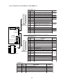
5 Portrait arrangement: Z-511J +Z-334J +Z-333J +Z-354J +Z-354J +Z-321J +Z-321J +Z-321J
Z-321J
8
Z-321J
Z-321J
Z-354J
Z-354J
7
Z-333J
Z-334J
6
5
4
Z-511J
3
2
1
Switch setting and I/O relay allocation
Mounting
SW1
(RACK NO)
SW2
(SWA)
1 2 3
1 2
2
None
1 2
3
None
1 2
1
4
5
6
7
8
1 2 3
1 2
1 2 3
1 2
1 2 3
1 2
1 2 3
1 2
1 2 3
1 2
I/O relay
address
コ 0000, 0001
コ 0002, 0003
コ 0004, 0005
コ 0006, 0007
コ 0010, 0011
コ 0012, 0013
コ 0014, 0015
コ 0016, 0017
コ 0020, 0021
コ 0022, 0023
コ 0024, 0025
コ 0026, 0027
Installed
address
R = 1, S = 0
R = 1, S = 1
R = 1, S = 2
R = 1, S = 3
R = 0, S = 0
R = 0, S = 1
R = 0, S = 2
R = 0, S = 3
R = 0, S = 4
R = 0, S = 5
R = 0, S = 6
R = 0, S = 7
コ 0030, 0031
コ 0032, 0033
コ 0034, 0035
コ 0036, 0037
コ 0040, 0041
コ 0042, 0043
コ 0044, 0045
コ 0046, 0047
コ 0050, 0051
コ 0052, 0053
コ 0054, 0055
コ 0056, 0057
コ 0060, 0061
コ 0062, 0063
コ 0064, 0065
コ 0066, 0067
コ 0070, 0071
コ 0072, 0073
コ 0074, 0075
コ 0076, 0077
R = 1, S = 4
R = 1, S = 5
R = 1, S = 6
R = 1, S = 7
R = 2, S = 0
R = 2, S = 1
R = 2, S = 2
R = 2, S = 3
R = 2, S = 4
R = 2, S = 5
R = 2, S = 6
R = 2, S = 7
R = 3, S = 0
R = 3, S = 1
R = 3, S = 2
R = 3, S = 3
R = 3, S = 4
R = 3, S = 5
R = 3, S = 6
R = 3, S = 7
-26-
ON
OFF
11. ROM operation
The ROM operation is a method of operating the Z-511J by the content of the ROM, by storing the
system memory or user program in the flash ROM, and transferring from the ROM to the RAM.
Saving of a program and more in the ROM is available, as the contents of the ROM do not disappear
after turning OFF the power.
ROM operation is convenient for the following systems:
• Operation frequency is low.
• No alternation of program and system memory.
• Requires registering or loading programs quickly.
With Z-511J series, flash ROMs are installed in the control module and so all the control module are
possible ROM operation.
(1) ROM operation method
The ROM operation is available in four types as shown in the table below, depending on the setting
value in the system memory #255. Set #255 depending on the use. (initial value is 000 OCT)
Setting value Transfer ROM to Data memory after
RAM (when
data transfer when
OCT HEX
power is ON)
power is ON.
Mode after data
transfer when
power is ON.
Transfer ROM to
RAM using a tool.
000
00
No
—
—
Available
021
11
Yes
Hold
Mode when the
power is OFF.
Available
042
22
Yes
Clear*
Stop
Available
104
44
Yes
Clear*
Run
Available
* The stored data in the ROM is maintained.
Note 1: A battery is necessary even in ROM operation.
Note 2: Before transfer data from the ROM to the RAM (when the power is ON, or using a tool),
make sure turn OFF the protect switch.
(2) Registerable contents to ROM
Areas that can be registered ROM is decided by setting value of system memory #256. (Initial value
is 200OCT.)
Setting value
Registerable contents to ROM
OCT
HEX
System memory
Program
Register
File 1
File 2
200
80
#200 to 2177
Yes
No
No
No
201
81
#200 to 2177
Yes
8K bytes *1
No
No
202
82
#200 to 2177
Yes
No
16K bytes
64K bytes *2
203
83
#200 to 2177
No
8K bytes *1
No
No
204
84
#200 to 2177
No
No
16K bytes
64K bytes *2
205
85
#200 to 2177
Yes
8K bytes *1
16K bytes
No
206
86
#200 to 2177
No
8K bytes *1
16K bytes
64K bytes *2
*1: 8 K bytes from 09000 to 99777 and E0000 to #57777. Area E6000 to E7777 cannot be stored in the
ROM.
(3) Writing in a flash ROM
By the writing operation by the hand-held programmer JW-13PG or the ladder software JW-92SP /
JW-52SP, the program can be written into flash ROMs of control modules.
See instruction manual of respective support tool for operation.
-27-
12. Upstream communication port
J-board Z-511J has upstream communication ports (communication port) (PG/ COMM1,PG/ COMM2).
The communication port can communicate with connected device having the I/O port of RS-232C/422A
of host computer, such as personal computer.
It can communicate the same as SHARP's computer link. When the support tool is not used, one set of
control module can have two channels of communication port, and two systems such as personal computer and liquid crystal control terminal can be connected.
Personal computer etc.
Only RS-422A
(Usable when the support tool
is not connected.)
Personal computer etc.
RS-232C or RS-422A
(Usable when the support tool
is not connected.)
Z-511J
COMM1
COMM2
"L" angle connector
COMM2
(RS422A)
Data link port
5 VDC Power source
Note
The "L" angle connector branches RS422A signals from the COMM2.
Therefore, if the D-sub 15-pin connector of the COMM2 is not used,
the "L" angle connector can be used as upstream communication
port.
Name
Function
COMM1 lamp
(orange)
• Flickers during communication by connecting PG/COMM1 port and
personal computer, etc.
COMM2 lamp
(orange)
• Flickers during communication by connecting PG/COMM2 port and
personal computer, etc.
PG/COMM1 port
(Only the RS-422A)
• Connect with support tool.
Usable as communication port (RS-422A only) when the support tool is
not used.
PG/COMM2 port
(RS-232C/422A)
• Connect with support tool.
Usable as communication port (RS-232C/422A) when the support tool is
not used.
-28-
[1] Pin arrangement of PG/COMM1 port, PG/COMM2 port
15 14 13 12 11 10 9
8
7
6
5
4
3
2
1
• PG/COMM1 port
Pin
No.
1
2
3
4
5
6
7
8
Signal
name
FG
--TxDA
--RTS(-)
SG
SG
---
9
RxDA
(15 pin D-sub
female connector) 10
RxDB
11 TxDB
12
--13 RTS(+)
14
+5V
15
+5V
COMM1
COMM2
Contents
Signal
Outside body grounding
--*
Sending data (PLC to personal computer) RS-422A
*
--RS-422A
Signal grounding
Signal grounding
--*
Receiving data (Personal computer to
PLC)
Receiving data (Personal computer to
RS-422A
PLC)
Sending data (PLC to personal computer)
*
--RS-422A
---
*: Not connected with pin No. 2, 4, 8, and 12.
COMM2
(RS422A)
• PG/COMM2 port
FG
2
3
4
5
L1
L2
L3
L4
8
7
6
1
5
4
3
2
5 VDC Power source
("L" angle connector)
15 14 13 12 11 10 9
1
Data link port
Pin Signal
Contents
No. name
1
FG Outside body grounding
2
SD Sending data (PLC to personal computer)
3
TxDA Sending data (PLC to personal computer)
Receiving data (Personal computer to
4
RD
PLC)
5 RTS(-)
6
SG Signal grounding
7
SG Signal grounding
8
RTS ON while PLC is supplied power source
(15 pin D-sub
Receiving data (Personal computer to
RxDA
female connector) 9
PLC)
Receiving data (Personal computer to
10 RxDB
PLC)
11 TxDB Sending data (PLC to personal computer)
12
CTS ON: Available sending, OFF: Ban sending
13 RTS(+)
14
+5V
15
+5V
• COMM2 port
Pin
number
1
2
3
4
5
Signal
name
FG
TxDA
TxDB
RxDA
RxDB
Description
Connect to the shield
Sending data (PLC to personal computer)
Sending data (PLC to personal computer)
Receiving data (Personal computer to PLC)
Receiving data (Personal computer to PLC)
-29-
Signal
RS422A
RS422A
RS422A
RS422A
Signal
RS-232C
RS-422A
RS-232C
RS-422A
_
RS-232C
RS-422A
RS-232C
RS-422A
-
[2] Wiring diagrams
(1) When using RS-232C for communication method of host computer side.
Be within 15m for the total length of a communication cable.
Z-511J
(PG/COMM2 port)
Host computer
Shielded wire
Signal name
Pin No. Signal name
1
FG
FG
2
SD
RD
4
RD
TD
8
RTS
CS
12
CTS
RS
7
SG
SG
Within 15m
RS-232C
Use the RS-232C/RS-422 converter, such as Z-101HE, when the total length of the communication
cable is over 15m.
Z-511J
RS-232C/RS-422 converter
PG/COMM1 port
(Z-101HE)
or PG/COMM2 port
Host computer
Pin No.
Signal name
Terminal block
name
Pin No.
Signal name
Signal name
3
TxDA
RD (+)
3
RD
RD
11
TxDB
RD (-)
2
TD
TD
9
RxDA
TD (+)
4
RS
RS
10
RxDB
TD (-)
7
SG
SG
1
FG
SHIELD
1
FG
FG
Shielded wire
Shielded wire
Class-3 grounding
Within 1km
RS-422A
Within 15m
RS-232C
(2) When using RS-422A for communication method
Be within 1km for the total length of a communication cable.
Z-511J
PG/COMM1 port
or PG/COMM2 port
Z-511J
PG/COMM1 port
or PG/COMM2 port
Host computer
Pin No.
Signal name
Pin No.
Signal name
Signal name
3
TxDA
3
TxDA
RXD
11
TxDB
11
TxDB
RXD
9
RxDA
9
RxDA
TXD
10
RxDB
10
RxDB
TXD
1
FG
1
FG
FG
Shielded wire
Within 1km
RS-422A
-30-
Shielded wire
[3] Setting of Z-511J system memory
Set system memory #234/#235 (communication port 1) and #236/#237 (communication port 2) for
communication conditions when communicating with a personal computer.
System memory
number
Description
#234
Transfer rate, parity, stop bit
#235
Station No. 001 to 037OCT
#236
Transfer rate, parity, stop bit
#237
Station No. 001 to 037OCT
Set communication port 1
(PG/COMM1 port)
Set communication port 2
(PG/COMM2 port)
(1) Setting of communication port 1 (PG/COMM1 port)
1 Setting of system memory #234
Specify transfer rate, parity, and stop bit as ON (1) / OFF(0) of D0 to D5.
D7
D6
D5
D4
D3
D2
D1
D0
#234
Stop bit
Parity
Transfer rate
D5
Stop bit
D4
D3
Parity
0
1 bit
0
0
None
1
2 bits
0
1
Add
1
0
Even
1
1
Data is fixed to 7 bits.
2 Setting of system memory #235
Set station No., 001 to 037OCT to communicate.
D2
0
0
0
0
1
1
1
1
D1
0
0
1
1
0
0
1
1
D0
0
1
0
1
0
1
0
1
Transfer rate(bits/s)
19200
9600
4800
2400
1200
115200
57600
38400
(2) Setting of communication port 2 (PG/COMM2 port)
1 Setting of system memory #236
Specify transfer rate, parity, and stop bit as ON (1) / OFF(0) of D0 to D5.
D7
D6
D5
D4
D3
D2
D1
D0
#236
Stop bit
Transfer rate
Parity
D5
Stop bit
D4
D3
Parity
0
1 bit
0
0
None
1
2 bits
0
1
Add
1
0
Even
1
1
Data is fixed to 7 bits.
2 Setting of system memory #237
Set station No., 001 to 037OCT to communicate.
-31-
D2
0
0
0
0
1
1
1
1
D1
0
0
1
1
0
0
1
1
D0
0
1
0
1
0
1
0
1
Transfer rate(bits/s)
19200
9600
4800
2400
1200
115200
57600
38400
[4] Communicate with a personal computer
The following instructions are available for communicating between the Z-511J and a personal computer. There are three type of command; read out command, write command and control command.
Command
Contents
Read out command
Messages that a personal computer transmits to the Z-511J when it
reads out data from the Z-511J.
Write command
Messages that a personal computer transmits to the Z-511J when it
reads out data from the Z-511J.
Control command
Messages that a personal computer transmits to the Z-511J when it
reads out data from the Z-511J.
As for the detail of each command, see "List of commands," and "Computer link" section of user's
manual of link module JW-21CM.
(1) Communication format
When a command from a personal computer is received, the communication port of Z-511J
operates according to the received command, and sends a response. When an error occurs
while processing, it returns an error response.
Z-511J
Personal computer etc.
COMM1
COMM2
COMM2
(RS422A)
1
Upstream
communication
2
5 VDC Power source
1 Communication format of command (personal computer to Z-511J)
Sum check area
A A
R
S S C
D D ? Command content C C I
(H) (L)
(H) (L) R
2 Communication format of response (Z-511J to personal computer)
Sum check area
A A
R
S S C
D D # Response content C C I
(H) (L)
(H) (L) R
Error response where an error occurs
Sum check area
A A
R E E S S C
D D % C C C C I (H) (L) (H) (L) R
(H) (L)
-32-
[Details of communication format]
*
*
*
Data
Code used
(ASCII character)
AD (H)
AD (L)
00 to 37OCT
RI
0 to FHEX
SC (H)
SC (L)
EC (H)
EC (L)
Description
Station No.
- In command, the station no. to be received command.
- In response, the station no. to send response.
Response time (Set the time from receiving a command to
responding. See page 35.)
Sum check code (Search the mistake of transfer data. Refer to next
page.)
00 to FFHEX
Error code (Indicate error content. Refer to the follows)
01 to 1BHEX
Identification
symbol
ASCII
code
: (colon)
? (question)
# (number mark)
% (percent)
3AHEX
3FHEX
23HEX
25HEX
Description
Header (Indicates beginning of command and response).
Indicates commands.
Indicates response (at normal).
Indicates response (at error).
Termination mark (Indicates termination of a command and
CR (carriage return)
0DHEX response).
* (H) indicates upper digit, (L) indicates lower digit.
• Details of error code
Error code
(EC (H), EC (L))
Description
01
Format error
02
Designated address is not TMR/CNT setting value
05
Number of transfer bytes is not correct
06
PLC does not stop by HLT (stop PLC processing)
07
Writing to PLC memory is not executed correctly
08
Memory capacity, file capacity is full
0A
Parity error
0B
Framing error
0C
Overrun error
0D
Sum check error
0E
Prohibit program memory write (memory protection switch "ON")
0F
Other CPU is accessing memory
10
Not match write mode
11
Not program area
12
Tried to write in ROM
1B
System memory error
30
A password is not yet registered.
31
The secret mode is not released.
32
Password register error.
(Tried to register other than alphabetical and numerical figures.)
33
The secret mode is not released.
-33-
• Sum check code SC (H), SC (L)
The communication port detects error using sum check as well as party check in order to increase the
reliability.
1) Sum check area (See page 32)
[Example] Command
Sumcheck area
A A
D D ?
(H) (L)
Command content
S S C
C C (H) (L) R
2) Check method
1. Add data from station No. to the last data of the command contents or response contents (just
before sum check code) that are summed up in ASCII code.
2. Convert the sum check code (2 digits hexadecimal) to 8 bits data and add 1) to the result.
When the grand total is "0" (disregarded figure up), the message is regarded as correct. When
the grand total is not "0," the message is regarded as an error.
3) Produce method
1. Add data from station No. to the last data of the command contents or response contents (just
before sum check code) that are summed up in ASCII code.
2. Operate complement number of 2 of the result of 1.
Complement number of 2: Turn over all the bits indicated by the binary system (0 to 1, 1 to 0)
and add 1.
[Example] The complement number of 2 of 4EHEX is B2HEX
4E → 01001110
↓ invert each bit
10110001
↓ add 1
10110010 → B2HEX
3. Divide upper 4 bits and lower 4 bits and convert them to ASCII code.
When sum check is not necessary, setting @ in the command line.
-34-
• Response time RI
When a personal computer is interpreter system, it executes programs one by one while interpreting.
This personal computer may not have finished its process before receiving the response from the Z511J. As a countermeasure, set response time RI of command (max. 600ms).
RI(HEX)
Response time (ms)
RI(HEX)
Response time (ms)
0
0
8
80
1
10
9
90
2
20
A
100
3
30
B
200
4
40
C
300
5
50
D
400
6
60
E
500
7
70
F
600
As the Z-511J accesses memories after one operation cycle, the actual response time is the total of
setting value of RI in command and the waiting time of one operation cycle.
[Reference] Setting response time RI
It is difficult to recommend the optimum response time, as the optimum response time is
varied depending on the model of personal computer, the programming language and
the system program. First, set a fairly long time, then, shorten gradually.
Note
There are some limitations for the number of bytes to handle by commands and for the communication buffer of personal computers. Be careful for the number of bytes to handle and communication
buffers.
(2) Write mode
Write mode of PLCs are "mode 0" (write prohibited for all memories) at power ON. Prior to writing
program from the personal computer, change write mode to "mode 1" or "mode 2" using EWR
command (setting of write mode). SWE command can be used to read out current status of
writing mode.
Set write mode to "mode 0" as much as possible, except when writing date into PLC. Each mode
has restrictions as follow:
Mode 0
Write prohibited for all memories
Mode 1
Write enable only for data memory
Mode 2
Write enable for all memories
Note
Turn OFF control module protect switch (write allowed) before executing write commands and change
to write mode 2 using EWR command.
-35-
Each command can be executed in the write mode or when the PLC is in the following state.
⃝ : Executable × : Non-executable
Write mode
Control command
Write command
Read-out command
Function
Relay monitor
Current value monitor of timer/counter/MD
Register current value monitor
Read out register of file 1
Read out register of file 0 to 3
Read out register of file 00 to 03, 10 to 2C
Read out parameter of special I/O module
Read out parameter of option module
Read out system memory
Read out program memory
Read out date
Read out time
Set/reset relay
Set/reset timer/counter
Write in register
Write the same data in register
Write in register of file 1
Write in register of file 0 to 3
Write in register of file 00 to 03, 10 to 2C
Write in parameter of special I/O module
Write in parameter of option module
Write in system memory
Write in program memory
Change setting value of timer/counter
Set date
Set time
Set time revision
Stop operation
Restart operation
Monitor operation conditions
Read memory capacity
Read out write mode status
Set write mode
Turn back the message
Release secret/password registration
Set secret function
Check secret function
Command
name
0
1
2
MRL
MTC
MRG
RFL
RFLF
(Note)RFLE
RPSR
RPS
RPO
RSM
RPM
MDY
MTM
SRR
SRT
WRG
FRG
WFL
WFLF
(Note)WFLE
WPSR
WPS
WPO
WSM
WPM
CTC
SDY
STM
ACL
HLT
RUN
MPC
VLM
SWE
EWR
TST
PAS
SES
SEI
○
○
○
○
○
○
○
○
○
○
○
○
○
×
×
×
×
×
×
×
×
×
×
×
×
×
×
×
×
○
○
○
○
○
○
○
*1
*2
○
○
○
○
○
○
○
○
○
○
○
○
○
○
○
○
○
○
○
○
○
×
×
×
×
×
×
○
○
○
○
○
○
○
○
○
○
*1
*2
○
○
○
○
○
○
○
○
○
○
○
○
○
○
○
○
○
○
○
○
○
○
○
○
○
○
○
○
○
○
○
○
○
○
○
○
○
○
○
○
PLC status
Stopped
by HLT
Run
command
○
○
○
○
○
○
○
○
○
○
○
○
○
○
○
○
○
○
○
○
○
○
○
○
○
○
○
○
×
○
○
○
○
○
○
○
○
○
○
○
○
×
○
×
○
×
○
×
○
×
○
○
○
○
○
○
○
○
○
○
○
○
○
○
○
○
○
○
○
○
○
○
○
*1
○
*2
○
○
*1: When data of command is 0, then, ⃝ . When data command is 1 or 2, then × .
*2: When data of command is 0, then, ⃝ . When data command is F, then × .
-36-
(3) Address expression system
In each command, the setting value in the following table is set in the address module of
communication format.
Relay number
Timer/counter point of contact
number
Timer/counter number
MD number
Register address
File register
address
Address
(octal)
Setting value
(octal)
00000 to 15777
00000 to 15777
20000 to 75777
20000 to 75777
T0000 to T1777
C0000 to C1777
T0000 to T1777
0000 to 1777
0000 to 1777
MTC, SRT
000 to 777
0000 to 1777
MTC
コ0000 to コ1577
A0000 to A1577
コ2000 to コ7577
B2000 to A7577
b0000 to b1777
B0000 to B1777
b2000 to b3777
B2000 to B3777
09000 to 09777
09000 to 09777
19000 to 19777
19000 to 19777
29000 to 29777
29000 to 29777
39000 to 39777
39000 to 39777
49000 to 49777
49000 to 49777
59000 to 59777
59000 to 5977
69000 to 69777
69000 to 69777
79000 to 79777
79000 to 79777
89000 to 89777
89000 to 89777
99000 to 99777
99000 to 99777
E0000 to E7777
E0000 to E7777
Using command
MRL, SRR
MRL
MRG, WRG,
FRG
File 0
000000 to 035777 000000 to 035777
File 1
File 2, 3
000000 to 037777 000000 to 037777 RFL, RFLF, RFLE
000000 to 177777 000000 to 177777 WFL, WFLF, WFLE
File 10 to 2C
000000 to 177777 000000 to 177777
Special I/O module parameter
address
Option module parameter address
System memory address
Z-511J(15.5K words)
000 to 177
0000 to 0177
RPSR, RPS
WPSR, WPS
00 to 77
0000 to 0077
RPO, WPO
#0000 to #2177
0000 to 2177
RSM, WSM
00000 to 36777
000000 to 036777
Program
address
RPM, WPM, CTC
-37-
(4) Data expression system
Data are expressed by hexadecimal. Program contents are also expressed by hexadecimal based
on machine language. Contents of bit configuration of program memory is not available.
(5) Example of communication (monitor current value of register)
Monitor from 09000 to 09003 of PLC06. (Response time : 100 ms)
Command
C
06? AM R G 09 00 0 0 9 0 03 3 F R
Station
Command
address
Response time
Register
address 1
Register
address 2
Sumcheck
code
Response
C
06# AM R G 09 00 0 0 9 0 03 0 0 4F3 2 0 1 E B R
Station
Command
address
Response time
Register
address 1
Register
address 2
-38-
Sumcheck
09002
09000
09003 code
09001
13. Data link port
The Z511J consists of a CPU section and a data link section. This data link section is identical to the
communication board Z-332J. However, it is compatible with the 4-wire system.
(1) Arrangement of data link ports
Z-511J
COMM1
COMM2
COMM2
(RS422A)
Data link port
5 VDC Power source
1
FG
2
3
4
5
L1
L2
L3
L4
("L" angle connector)
- Data link port (compatible with the 4-wire system)
Pin
Signal
Description
number name
1
FG Connect to the shield
2
L1 Sending data (PLC to personal computer)
3
L2 Sending data (PLC to personal computer)
4
L3 Receiving data (Personal computer to PLC) (4-wire system only)
5
L4 Receiving data (Personal computer to PLC) (4-wire system only)
-39-
Signal
RS422A
RS422A
RS422A
RS422A
(2) Connection examples
a. When the Z-511J is used as a data link slave station
Twisted pair shield cable
L1
L2
SHIELD
FG
Master station
JW-10CM
L1
L2
SHIELD
FG
Slave station 01
JW-10CM
Class-3
grounding
L1
L2
L3
Ground
Slave station 02
ZW-160DL9
Class-3
grounding
L1
L2
L3
Ground
Slave station 03
ZW-501D9
Class-3
grounding
L1
L2
FG
FG
Slave station 17
Z-511J
Class-3
Class-3
grounding grounding
Total cable length:1 km or less
Max. number of connectable slave station:15
b. When the Z-511J is used as in computer link mode
- 4-wire system
RS-232C/422
converter Z-101HE
Host computer
FG
TD
RD
SG
Frame ground
Sending data
Receiving data
Signal ground
1
2
3
7
FG
TD
RD
SG
PLC01 for W100
ZW-1K0CL2
PLC02 for JW100H
JW-10CM
Z-511J
TD (+)
L3
L3
L3
TD (−)
RD (+)
RD (−)
L4
L4
L4
L1
L2
L1
L2
SHIELD
SHIELD
SHIELD
L1
L2
FG
FG
GND
Class-3 grounding
Twisted pair shield cable
Shield cable
15 m or less
Cable total length: 1 km or less
RS-232C
RS-485
- 2-wire system
RS-232C/422
converter Z-101HE
Host computer
FG
TD
RD
RS
SG
Frame ground
Sending data
Receiving data
Request to send
Signal ground
1
2
3
4
7
FG
TD
RD
RS
SG
PLC01 for W10
ZW-10CL2
RD (+)
RD (−)
SHIELD
PLC02 for W16/51
ZW-160CL2/501CL2
PLC17 for W100
ZW-1K0CL2
L1(T1)
L2(T2)
L3
L1
L2
FG
L1
L2
SHIELD
Ground
Class-3
grounding
Class-3
grounding
Class-3
grounding
Z-511J
L1
L2
FG
FG
Twisted pair shield cable
Shield cable
15 m or less
Cable total length: 1 km or less
RS-232C
RS-485
(3) How to use the data link port
For specific details about using the data link port, see the "JW21CM User's Manual" and the
"Commu nication board: Z-331J/332J/333J User's Manual."
-40-
14. Items the user must supply
Please supply the following parts yourself.
Connectors for the upstream communication port and power line.
Connector
Connector name
Mfg.
Applicable connector
number
CN5
Upstream communication port Molex CN: 5265-N, Terminal: 2578G
CN4
Data link port
Molex CN: 5265-N, Terminal: 2578G
CN3
5V DC power
Molex CN: 51102-0500, Terminal: 50351-8100
-41-
SHARP MANUFACTURING SYSTEMS CORPORATION
♦ Information about Sharp image sensor camera and programmable controller
is available at our internet homepage
http://sharp-world.com/sms/
1.0v
10.2005
(0.1I.M.S)