1
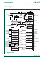
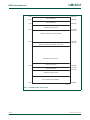
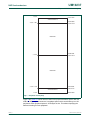
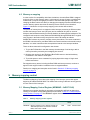
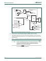
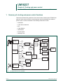
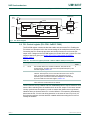
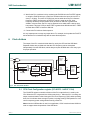
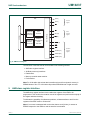
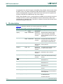
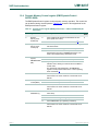
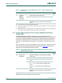
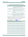
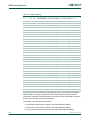
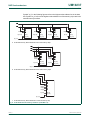
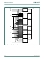
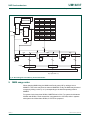
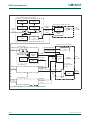
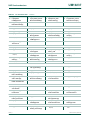
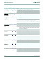
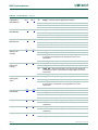
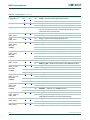
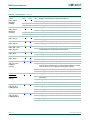
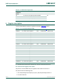
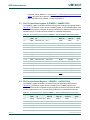
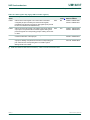
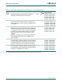
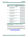
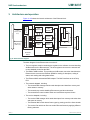
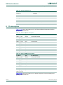
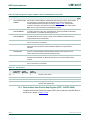
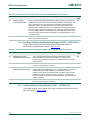
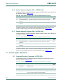
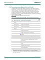
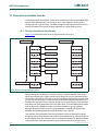
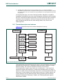
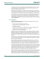
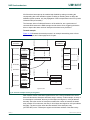
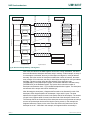
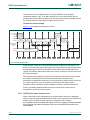
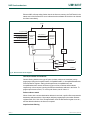
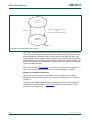
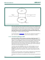
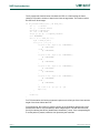
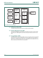
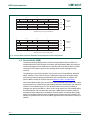
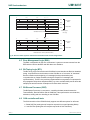
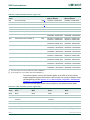
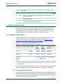
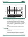
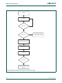
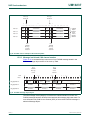
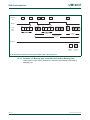
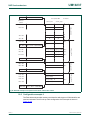
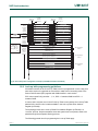
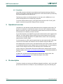
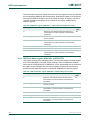
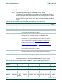
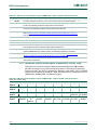
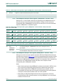
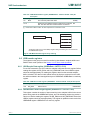
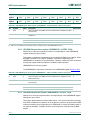
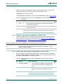
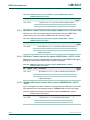
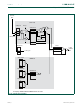
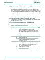
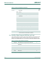
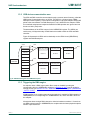
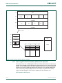
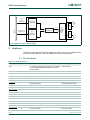
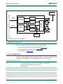
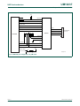
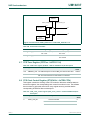
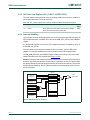
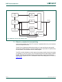
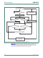
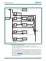
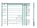
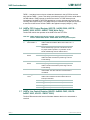
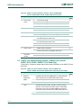
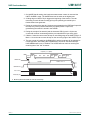
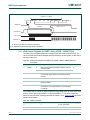
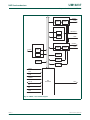
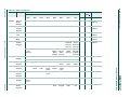
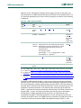
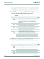
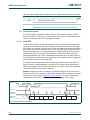
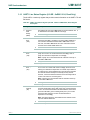
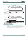
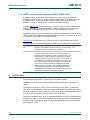
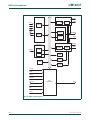
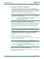
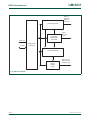
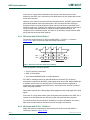
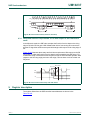
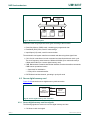
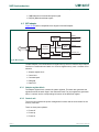
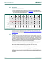
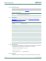
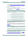
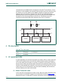
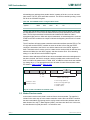
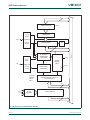
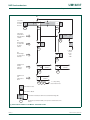
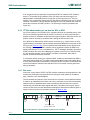
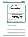
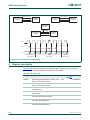
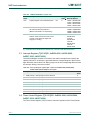
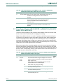
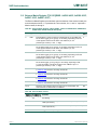
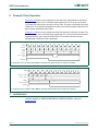
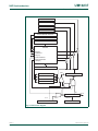
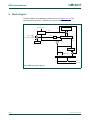
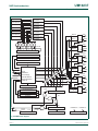
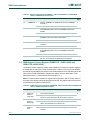
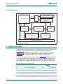
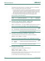
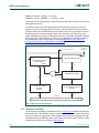
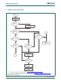
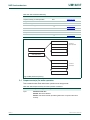
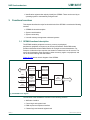
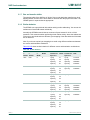
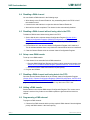
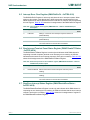
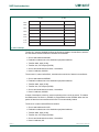
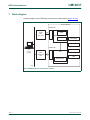
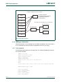
UM10237
NXP Semiconductors
Chapter 4: LPC2468 clocking and power control
Table 20.
Clock Source Select register (CLKSRCSEL - address 0xE01F C10C) bit
description
Bit Symbol
Value Description
1:0 CLKSRC
Reset
value
Selects the clock source for the PLL as follows:
0
00
Selects the Internal RC oscillator as the PLL clock source
(default).
01
Selects the main oscillator as the PLL clock source.
10
Selects the RTC oscillator as the PLL clock source.
11
Reserved, user software should not write ones to reserved bits.
The value read from a reserved bit is not defined.
Warning: Improper setting of this value, or an incorrect sequence of
changing this value may result in incorrect operation of the device.
7:2 -
0
Unused, always 0.
0
5. PLL (Phase Locked Loop)
The PLL accepts an input clock frequency in the range of 32 kHz to 50 MHz . The input
frequency is multiplied up to a high frequency, then divided down to provide the actual
clock used by the CPU and the USB block.
5.1 PLL operation
The PLL input, in the range of 32 kHZ to 50 MHz, may initially be divided down by a value
"N", which may be in the range of 1 to 256. This input division provides a greater number
of possibilities in providing a wide range of output frequencies from the same input
frequency.
Following the PLL input divider is the PLL multiplier. This can multiply the input divider
output through the use of a Current Controlled Oscillator (CCO) by a value "M", in the
range of 1 through 32768. The resulting frequency must be in the range of 275 MHz to
550 MHz. The multiplier works by dividing the CCO output by the value of M, then using a
phase-frequency detector to compare the divided CCO output to the multiplier input. The
error value is used to adjust the CCO frequency.
There are additional dividers at the PLL output to bring the frequency down to what is
needed for the CPU, USB, and other peripherals. The PLL output dividers are described
in the Clock Dividers section following the PLL description. A block diagram of the PLL is
shown in Figure 4–8
PLL activation is controlled via the PLLCON register. The PLL multiplier and divider
values are controlled by the PLLCFG register. These two registers are protected in order
to prevent accidental alteration of PLL parameters or deactivation of the PLL. Since all
chip operations, including the Watchdog Timer, could be dependent on the PLL if so
configured (for example when it is providing the chip clock), accidental changes to the PLL
setup could result in unexpected or fatal behavior of the microcontroller. The protection is
accomplished by a feed sequence similar to that of the Watchdog Timer. Details are
provided in the description of the PLLFEED register.
The PLL is turned off and bypassed following a chip Reset and by entering Power-down
mode. PLL is enabled by software only.
UM10237_1
User manual
© NXP B.V. 2006. All rights reserved.
Rev. 01 — 18 December 2006
31 of 664