1
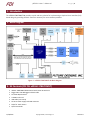
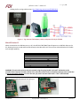
µEZGUI User’s Manual Covers the following products: uEZGUI-1788-70WVT (Dev Kit) uEZGUI-1788-70WVT-BA (Board Assembly) Copyright ©2014, Future Designs, Inc., All Rights Reserved µEZGUI User’s Manual P a g e |2 Table of Contents 1. Introduction _________________________________________________________________________________ 4 2. Block Diagram ________________________________________________________________________________ 4 3. Kit Contents (FDI PN: uEZGUI-1788-70WVT) ________________________________________________________ 4 4. Useful links __________________________________________________________________________________ 5 5. Functional Description _________________________________________________________________________ 5 6. Startup procedure_____________________________________________________________________________ 6 7. Demonstration Software Main Menu _____________________________________________________________ 6 8. Setting up a Slideshow _________________________________________________________________________ 8 9. Setting up a Video _____________________________________________________________________________ 8 10. uEZ Doxygen online HTML documentation _________________________________________________________ 8 11. uEZ Project Maker_____________________________________________________________________________ 9 12. Software ____________________________________________________________________________________ 9 13. Configuring Rowley CrossWorks CrossStudio for ARM® for J-Link Flashing _______________________________ 10 14. Configuring IAR EWARM v6 for J-Link Flashing _____________________________________________________ 11 15. Configuring Keil uVison 4 for J-Link Flashing _______________________________________________________ 12 16. Functional Test Software ______________________________________________________________________ 13 17. Board Layout ________________________________________________________________________________ 14 18. I/O Connector Descriptions ____________________________________________________________________ 15 JTAG Connector J5 __________________________________________________________________________ 15 Tag Connect J12 ____________________________________________________________________________ 15 ISP Connector J3 (not loaded) _________________________________________________________________ 17 Alternate Power and communication J11 (loaded) _________________________________________________ 18 P1 – USB mini-AB port _______________________________________________________________________ 18 P2 – USB Power Input 5VDC ___________________________________________________________________ 18 Expansion Connectors J4 & J5 _________________________________________________________________ 19 Expansion Connector Cable Details _____________________________________________________________ 22 19. Schematics _________________________________________________________________________________ 23 20. Temperature Range __________________________________________________________________________ 23 21. Real Time Clock Backup Time ___________________________________________________________________ 23 22. ESD Warning ________________________________________________________________________________ 23 23. Power Requirements _________________________________________________________________________ 23 24. Mechanical Details ___________________________________________________________________________ 24 25. Dimension comparison between 70WVE and 70WVT models _________________________________________ 25 11/18/2014 Copyright ©2014, Future Designs, Inc Revision 5 µEZGUI User’s Manual P a g e |3 Important Legal Information Information in this document is provided solely to enable the use of Future Designs products. FDI assumes no liability whatsoever, including infringement of any patent or copyright. FDI reserves the right to make changes to these specifications at any time, without notice. No part of this document may be reproduced or transmitted in any form or by any means, electronic or mechanical, for any purpose, without the express written permission of Future Designs, Inc. 996 A Cleaner Way, Huntsville, AL 35805. For more information on FDI or our products please visit www.teamfdi.com. NOTE: The inclusion of vendor software products in this kit does not imply an endorsement of the product by Future Designs, Inc. 2014 Future Designs, Inc. All rights reserved. uEZ® is a registered trademark of Future Designs, Inc. Microsoft, MS-DOS, Windows, Windows XP, Microsoft Word are registered trademarks of Microsoft Corporation. Other brand names are trademarks or registered trademarks of their respective owners. FDI PN: MA00039 Revision: 1.0, 10/03/2014 Printed in the United States of America 11/18/2014 Copyright ©2014, Future Designs, Inc Revision 5 µEZGUI User’s Manual P a g e |4 1. Introduction The uEZGUI-1788-70WVT-BA provides a quick and easy solution for implementing a Graphical User Interface (GUI) based design by providing the basic functions necessary for most customer products. 2. Block Diagram Figure 1 – uEZGUI-1788-70WVT-BA Block Diagram 3. Kit Contents (FDI PN: uEZGUI-1788-70WVT) uEZGUI-1788-70WVT-BA Resistive Touch Screen Kit with LCD Segger Mini-JTAG Debugger and JTAG cable FDI JTAG Adapter Board 4 GB Micro SD card USB Cable (A to mini B) 5V 2A AC Power supply with USB connector Stylus for Touch Screen Quick Start Guide 11/18/2014 Copyright ©2014, Future Designs, Inc Revision 5 µEZGUI User’s Manual P a g e |5 4. Useful links Complete Users Manuals, Schematics, and documentation are available on the Micro-SD card provided with the uEZGUI Kit and are also available from the following websites (please refer to the websites for the latest updates): Future Designs Support Page - http://www.teamfdi.com/support/ uEZ Source Code, users manuals, and quickstart guides - https://sourceforge.net/projects/uez/ Segger Mini-JTAG Debugger - http://www.segger.com/cms/jlink-software.html Rowley Crossworks IDE download for 30-day evaluation - http://www.rowley.co.uk/arm/index.htm 5. Functional Description LPC1788 Cortex-M3 based Microprocessor SDRAM 16MB, optional up to 32MB NOR FLASH 8MB, optional up to 16MB Serial EEPROM with Access Protection (optional) Internal 4kB EEPROM RTC – Real Time Clock Temperature Sensor 3-axis Accelerometer Optional 128Mbit Serial Flash Optional Wi-Fi Module Speaker Micro-SD Card Socket for up to 64GB storage Mini JTAG Power-on Reset Generator - power-on reset supervisor and voltage monitor (SW1) Expansion Connector for customer specific applications USB Host or Device support through mini B/AB connector and adapter 11/18/2014 Copyright ©2014, Future Designs, Inc Revision 5 µEZGUI User’s Manual P a g e |6 6. Startup procedure The uEZ GUI kit comes with a pre-installed Micro SD card that contains files required for the slide show and videos to run. It also contains users’ manuals, schematics, and documentation for the product. Power is supplied via a USB cable and power supply provided in the kit. Connect the USB cable from the power supply to (P2) the mini B USB connector labeled 5V 1A min input only. Note that the other USB connector (P1) is for communications only and will not supply power to the unit. Also note that the minimum power requirement is 1.0A so most USB power sources, which are limited to 500mA max, will not adequately power this unit. The following screens should appear once power has been applied to the kit: At this point the unit is ready for software demonstrations and user operation. By connecting the USB A to mini B cable to P1, the uEZGUI will also appear as a USB Flash Drive to the PC, allowing the user to read/write files directly to the Micro SD card. 7. Demonstration Software Main Menu The Demonstration Software has the following options: Slideshow Selecting the slideshow icon will cause the Micro SD card to be read. This demonstration allows the user to select between several slideshow options such as “uEZGUI Family Overview”, “Demonstration Pictures”, “uEZ Software 11/18/2014 Copyright ©2014, Future Designs, Inc Revision 5 µEZGUI User’s Manual P a g e |7 Overview”, “Modular Development Kit”, etc. Select the slideshow to view by touching the menu entry for it on the touch screen. By touching the screen during the slideshow, the menu overlay will appear. Select the play button (green) to begin the automated slide show. Touch the “||” button to pause the slideshow. The user can switch to the next slide by touching the “>” or “<” menu buttons, or by “dragging” the screen up or down. Click on the “X“ to return to the main menu. The following programs appear under the “Apps” icon: Accelerometer Selecting this icon demonstrates the accelerometer feature by moving a simulated ball across the screen as the board is tilted along the X and Y axis. To return to the main menu touch the exit icon. Time and Date This feature displays the current time and date from the internal Real Time Clock (RTC). To change the time or date simply click on the section you want to change and increase or decrease using the up and down indicators. Once set an on-board super capacitor will back-up the time and date for several days (typically) if the unit is powered off. To return to the main menu touch the exit icon. Temperature Selecting this icon displays the temperature from the LM75 temperature sensor. To select between Celsius and Fahrenheit click the “C’ or “F” to change. To return to the main menu touch the exit icon. Exit the “Apps” Icon to the main screen and the following programs are available The following programs appear under the “Communications” icon: Console This option is only valid with either the uEZGUI-EXP1 or uEZGUI-EXP-DK attached with an active Ethernet connection. Select the icon to start a telnet server on port 23. Telnet to port 23 on the unit’s IP address from a PC to access the standard serial console over a telnet connection. The following programs appear under the “Settings” icon: Brightness Selecting the brightness icon shows a menu with color bars and a brightness adjustment slider. Move the slider up or down to adjust the brightness. There is a check box in this menu that can turn the screensaver demonstration on or off. By default it is turned off. When enabled, the screensaver will dim the screen and then display a moving uEZ logo icon all over the screen. When the screen is touched again, it will return back to the current menu view. Calibrate Use this feature to calibrate the LCD for the first time or if corrections are required. This feature draws 5 targets on the screen. They should be pressed as they appear using the provided stylus. If the calibration data is valid it will be saved. This menu will also appear if the touch screen is pressed during boot-up. 11/18/2014 Copyright ©2014, Future Designs, Inc Revision 5 µEZGUI User’s Manual P a g e |8 Functional Test is a step by step test of the following parameters: Speaker test LCD color test SDRAM size test Temperature EEPROM test NOR Flash Memory test Draw A very simple art program is provided. Use the touch screen to draw lines in the box to the right. Clicking on Color allows the color to be changed between various options. Hint – use black to erase. Save stores the graphic image as the file IMAGE.RAW on the Micro SD card. Load recalls the saved graphic image from the Micro SD card. emWin Demo If present, this runs a demonstration of various emWin graphical demos. See http://www.segger.com/emwin.html for more details. This example is available here for reference: http://www.segger.com/emwin-samples.html 8. Setting up a Slideshow The Slideshow demonstration loads and scrolls between images provided on a SD micro card. Images must be in 24 bit uncompressed Targa (.TGA) format. Adobe Photoshop and many other graphics programs can save images in this format. The images must be 800x480 and 11.11”x6.67” in size and use the file names WVSLIDExx.TGA where xx is 00 thru 99. (i.e. WVSLID01.tga, WVSLID02.tga, etc). Images must be stored in a directory under /SLIDES. Edit the file “SLIDES.TXT” by adding a line in the following format: “<title>,<directory>”. The field <title> is the text shown when selecting a slideshow. The field <directory> is the subdirectory in which the slides are found. The field <directory> must be 8 characters or less. NOTE: Currently, the uEZ GUI will only allow selection of the top four entries of “SLIDES.TXT”. Place the pictures created above in the subdirectory listed in the “SLIDES.TXT” file. For example, entry “uEZGUI1788-70WVT,UEZGUI” puts up a title of “uEZGUI-1788-70WVT” and loads the slides (WVSLID01.TGA to WVSLID08.TGA) from the directory /SLIDES/UEZGUI. 9. Setting up a Video Refer to the “uEZ Video Conversion Guide” for details on converting a video for playback on a uEZGUI. The guide covers the video conversion process, as well as how to setup the video files on a microSD card for playback in the uEZ video player. 10. uEZ Doxygen online HTML documentation μEZ® has built-in comment documentation that follows the Doxygen comment standard. 11/18/2014 Copyright ©2014, Future Designs, Inc Revision 5 µEZGUI User’s Manual P a g e |9 This standard allows for code comments and annotations to be written in a certain manner, and then compiled along with source code into HTML documentation. FDI provides the pre-compiled HTML documentation at this link: http://www.teamfdi.com/uez/docs/ In the uEZ source code, “uEZ/uEZDoxyfile” is the main project file for the Doxygen generator. When Doxygen is recompiled, the new Doxygen files will be found here: uEZ\Docs\ Doxygen_Documentation.html FDI will update the documentation roughly with each new μEZ® release or as new drivers are added to the system. For more information, see the Doxygen website: http://www.doxygen.org/ 11. uEZ Project Maker FDI has provided a project maker to help create new projects for uEZGUI hardware. The project maker is included in the uEZ source code download package and includes its own user’s manual. This project maker can create demo projects using a very simple emWin example GUI, along with some basic peripheral functionality. The project maker greatly speeds up the development process for new applications. Example projects are ready to be compiled and programmed onto uEZGUI hardware using the included J-Link debugger, with no extra project configuration necessary. 12. Software μEZ® takes its name from the Muses of Greek mythology. A Muse was a goddess who inspired the creation process for the arts and sciences. Like its ancient Greek namesake, the μEZ® platform inspires rapid development by supplying customers with an extensive library of open source software, drivers, and processor support - all under a common framework. μEZ® development works on the premise of ”design once, reuse many times”. This provides an open source standard for embedded developers to build upon and support. μEZ® allows companies to focus on innovation and on their own value-added applications while minimizing development time and maximizing software reuse. The diagram below shows a typical embedded application stack. μEZ® has three primary categories of components that help simplify embedded application development: 1. Operating System Abstraction Layer (μEZ® OSAL) 2. Sub-system drivers (μEZ® TCP/IP, μEZ® USB, μEZ® Driver) 3. Hardware Abstraction Layer (μEZ® HAL) 11/18/2014 Copyright ©2014, Future Designs, Inc Revision 5 P a g e | 10 µEZGUI User’s Manual Applications µEZ® OSAL µEZ® TCP/IP µEZ® USB Host Device OTG Iwip µEZ® DRIVER LCD Touchscreen File System I2C, SPI, Etc. FreeRTOSTM µEZ® HAL Hardware Peripheral API Embedded Microprocessor The selection of an RTOS can be one of the most daunting aspects of an embedded system development. With μEZ® the primary features of common multi-tasking operating systems are abstracted, thus easing the transition to an open source or low-cost RTOS. The μEZ® OSAL provides applications access to the following features in an OSindependent fashion: Pre-emptive multitasking Stack overflow detection Unlimited number of tasks Queues Semaphores (binary, counting, mutex) The μEZ® sub-system drivers utilize the OSAL functions to provide protected access to the processor peripherals. The sub-system driver API functions are typically protocol layer interfaces (TCP/IP, USB, etc) designed as high-level access routines such as open, close, read, write, etc. where possible. μEZ® is ideally suited for Embedded Systems with standard features such as: Processor and Platform BSPs TCP/IP stack (Board Support Packages) USB Device/Host Libraries Real Time Operating System (RTOS) Mass Storage Devices Memory Management LCD Displays with Touch Screen NAND/NOR Flash Input / Output Devices SDRAM and DDR Memory 13. Configuring Rowley CrossWorks CrossStudio for ARM® for J-Link Flashing 1) See the document “uEZ® Software Quickstart Guide” for details on how to download the uEZ® source code and setup the Rowley CrossWorks compiler. (http://www.teamfdi.com/development-tools-kits/uez.php) software quick start guide 2) Plug in the J-Link device into the PC and install any drivers as directed. The Segger J-Link drivers can be found at http://www.segger.com/cms/jlink-software.html with additional information at http://www.segger.com/cms/development-tools.html. 3) Plug in the J-Link’s JTAG connector to the uEZGUI board at J3 with the JTAG adapter. 11/18/2014 Copyright ©2014, Future Designs, Inc Revision 5 µEZGUI User’s Manual P a g e | 11 4) Select Target menu and choose Targets. The following list will appear to the right. 5) Right click on “Segger J-Link” and select Properties 6) If programming a blank LPC1788 part, select a Speed of 100. If the part has already been programmed, select a Speed of 1000. 7) Go back to menu Target and select “Connect Segger J-Link” 8) Compile the application and press F5 to download and start debugging. 14. Configuring IAR EWARM v6 for J-Link Flashing The IAR tools do not require any special configuration for configuring the J-Link tools. To update IAR’s J-Link dll you just need to run Segger’s J-Link DLL Updated and select the IAR install you wish to update and click Ok. 11/18/2014 Copyright ©2014, Future Designs, Inc Revision 5 µEZGUI User’s Manual P a g e | 12 15. Configuring Keil uVison 4 for J-Link Flashing To configure Keil, use the following steps. 1. Click Flash from the Menu Bar and select Configure Flash Tools… 2. Click the Utilities Tab. 3. In the dropdown box for Use Target Driver for Flash Programming select the CORTEX-M/R J-LINK/J-Trace. 4. Click the Debug tab and select the same device for Use. 11/18/2014 Copyright ©2014, Future Designs, Inc Revision 5 µEZGUI User’s Manual P a g e | 13 16. Functional Test Software The Functional Test Software tests all the basic features of the uEZGUI-1788-70WVT KIT as follows. Functional Test - a step by step test of the following parameters: Accelerometer – Tests the presence of the accelerometer. EEPROM test - The EEPROM is tested for communication and integrity. LCD color test - Red, Green, and Blue are displayed in smooth bands to ensure the LCD lines are correct MicroSD – Looks for a Micro SD Card with the file “SLIDES/SLIDES.TXT” NOR Flash Memory test - basic test is performed to confirm read/write access. RTC – Sets the time and confirms the clock is running. SDRAM size test - Memory is sized and a basic test is performed to confirm read/write access. Speaker test - Tones are played and the User is asked to verify that they are heard. Temperature – the board has an external LM75A that is tested to be in a range of 20-30 C. A final report of PASS or FAIL is displayed along with a list of any Skipped and Failed items. 11/18/2014 Copyright ©2014, Future Designs, Inc Revision 5 µEZGUI User’s Manual P a g e | 14 17. Board Layout The following figures illustrate the layout of the various components of the uEZGUI-1788-70WVT-BA kit. They are for reference only and are subject to change. Figure 2 –uEZGUI-1788-70WVT Component View 11/18/2014 Copyright ©2014, Future Designs, Inc Revision 5 µEZGUI User’s Manual P a g e | 15 18. I/O Connector Descriptions JTAG Connector J5 The uEZGUI-1788-70WVT-BA uses a reduced size JTAG connector based on a 2mm Header. This smaller connector provides 100% of the functionality of the standard 20-pin JTAG connector, but utilizes 70% less board space. The connector is a standard part available from most major vendors. Pin Number Description Pin Number Description 1 2 3 4 5 GND 5.0V TDO RESETn TCK 6 7 8 9 10 RTCK TDI TMS 3.3V TRSTn For users that may have existing JTAG debuggers, an adapter may be fabricated using the following wiring diagram: (part numbers for the connectors are included from both the manufacturer and Digi-Key) Figure 3 – Mini JTAG Adapter Schematic Tag Connect J12 The uEZGUI-1788-70WVT-BA also includes the ability to JTAG and program using the Tag-Connect TC2050ARM2010 ARM 20-pin to TC2050 Adapter. Adapter: http://www.tag-connect.com/TC2050-ARM2010 Cable with legs: http://www.tag-connect.com/TC2050-IDC Cable with no legs: http://www.tag-connect.com/TC2050-IDC-NL 11/18/2014 Copyright ©2014, Future Designs, Inc Revision 5 µEZGUI User’s Manual P a g e | 16 Holding clip for no-legs cable version: http://www.tag-connect.com/TC2050-CLIP Figure 4 – Tag-Connect JTAG adapter, cables, and pinout for 10-pin TC2050 MicroSD Socket J2 When connected to the USB Host port on a PC, the uEZGUI-1788-70WVT-BA will appear as a USB Flash Drive to the PC, allowing the user to read and write files directly to the MicroSD card. The unit uses a MicroSD Socket for flexible mass storage capability. Pin Number 1 2 3 4 5 6 7 8 Description NC Micro SD Chip Select Micro SD MOSI 3.3V Micro SD SCLK Ground Micro SD MISO NC WARNING: The microSD card must only be removed using the spring loaded “push-pull” mechanism on the microSD socket. Improper forceful removal of the microSD card will result in permanent damage to the socket that is not covered under warranty. To insert the card, just push it into the socket until a “click” sound is heard. Start with the microSD card in this position relative to the microSD slot with the text and “lip” facing up. 11/18/2014 Next gently insert the card partially into the socket. Copyright ©2014, Future Designs, Inc Revision 5 µEZGUI User’s Manual Use your figure to gently push the card into the socket until it clicks. P a g e | 17 At this point the microSD card is fully inserted. It should not fall out, even if the unit is shaken vigorously. To remove the microSD card, press the card back into the socket until another “click” sound is heard, then release pressure on the card. At this point, the card should be partially ejected from the socket. Finally grab the card and gently pull to remove it. See the following pictures for proper micro-SD removal: To remove the microSD card, gently push it into the At this point, the microSD card should partially stick out socket again until it “clicks”, and then release your figure. of the socket. Carefully grab the edges or sides of the microSD card and gently pull it out. At this point the microSD card is fully removed from the socket. ISP Connector J3 (not loaded) The uEZGUI-1788-70WVT-BA is laid out with an ISP programming header. This header is designed to be utilized with the USB-ICP-LPC2K programmer from FDI. However the connector on the uEZGUI-1788-70WVT11/18/2014 Copyright ©2014, Future Designs, Inc Revision 5 µEZGUI User’s Manual P a g e | 18 BA is not directly compatible with the one used on the USB-ICP. This connector is a 1.25mm Hirose male, shrouded connector. The Hirose Part Number is: DF13A-6P-1.25H(20) (Digikey PN: H3371-ND). The pin out shown below is a direct, 1:1 connection to the USB-ICP-LPC2K programmer available from Future Designs, Digi-Key or Mouser. Pin Number Description 1 2 3 4 5 6 3.3V Reset Input ISP Entry Ground RXD TXD Alternate Power and communication J11 (loaded) The uEZGUI-1788-70WVT-BA is laid out with an alternate power and communication header. This header provides access to UART 3, as well as a 5V power input. This connector is a 1.25mm Hirose male, shrouded connector. The Hirose Part Number is: DF13A-6P-1.25H(20) (Digikey PN: H3371-ND). Pin Number Description 1 2 3 4 5 6 P0.10_TXD2_SDA2 5V Input 5V Input Ground Ground P0.11_RXD2_SCL2 P1 – USB mini-AB port The uEZGUI-1788-70WVT-BA has a mini-AB USB connector for host or device mode. By using a USB OTG adapter (with a mini-A plug) it will short the ID pin 4 to ground. This can be used for host mode detection in the application. Pin Number Description 1 2 3 4 5 5V DD+ ID Ground P2 – USB Power Input 5VDC The uEZGUI-1788-70WVT is normally powered via P2 with the included 5V USB Wall Supply. This power supply is only included in the development kit and is not included with the uEZGUI-1788-70WVT-BA. Note that the other USB connector (P1) is for communications only and will not supply power to the unit. Also note that the minimum power requirement is 1.0A so most USB power sources, which are limited to 500mA max, will not adequately power this unit. 11/18/2014 Copyright ©2014, Future Designs, Inc Revision 5 µEZGUI User’s Manual Pin Number Description 1 2 3 4 5V No Connect No Connect Ground P a g e | 19 Expansion Connectors J4 & J5 The uEZGUI-1788-70WVT-BA includes two expansion connectors that provide a wide variety of capabilities for user expansion, ranging from 10/100 Ethernet to USB Host, etc. The tables below provide the pinout and signal names available on these connectors: J4 Signal Details Pin Pin Name 1 Ground (GND) 2 P0.11_RXD2_SCL2_MAT3.1 3 P0.10_TXD2_SDA2_MAT3 4 P0.20_DTR1_SCL1 5 P0.19_DSR1_SDA1 6 P0.22_RTS1 7 P0.17_CTS1_MISO_MISO0 8 P0.16_RXD1_SSEL0 9 P0.15_TXD1_SCK0_TXD1_SCK 10 Ground (GND) 11 USB1_DM 12 USB1_DP 13 USB1H_PWRD 14 USB1H_OVC 15 USB1H_PPWR 11/18/2014 Pin Description P0[11] - General purpose digital Input/Output pin. RXD2 - Receiver input for UART2. SCL2 - I2C2 clock Input/Output (this is not an open-drain pin) MAT3[1] -Match output for Timer3, channel 1. P0[10] - General purpose digital input/output pin. SDA2 - I2C2 data input/output (this is not an open-drain pin). MAT3[0] - Match output for Timer3, channel 0. TXD2 -Transmitter output for UART2. P0[20] - General purpose digital input/output pin. DTR1 - Data Terminal Ready output for UART1 SCL1 - I2C1 clock input/output (this is not an open-drain pin) P0[19] - General purpose digital input/output pin. SDA1-I2C1 data input/output (this is not an open-drain pin). DSR1 - Data Set Ready input for UART1. P0[22] - General purpose digital input/output pin. RTS1 - Request to Send output for UART1. P0 [17] - General purpose digital input/output pin CTS1 - Clear to Send input for UART1. MISO - Master In Slave Out for SPI. MISO0 - Master In Slave Out for SSP0. Power I/O I I/O O I/O I/O O O I/O O I/O I/O I/O I I/O O I/O I I/O I/O P0[16] - General purpose digital input/output pin. I/O SSEL0 - Slave Select for SP0. RXD1 - Receiver input for UART1. P0[15] - General purpose digital input/output pin. SCK0 - Serial clock for SSP0. TXD1 – Transmitter output for UART1. SCK - Serial clock for SPI. I/O I I/O I/O O I/O Power I/O I/O I/O I/O I/O O I/O I/O I P0[30] - General purpose digital Input/Output pin. USB_D- 1 - USB port 1 bidirectional D- line. P4[29] - General purpose digital Input/Output pin. USB_D+1 - USB port 1 bidirectional D+ line. P4[26] -General purpose digital Input/Output pin. BLS0 - LOW active Byte Lane select signal 0. P4[24] - General purpose digital Input/Output pin. P0[19] - General purpose digital Input/Output pin. CAP1[1] - Capture input for Timer 1, channel 1 Copyright ©2014, Future Designs, Inc Revision 5 µEZGUI User’s Manual 16 17 18 19 P0.9_I2STX_SDA_MOSI1_MAT2.3 P0.8_I2STX_WS_MISO1_MAT 2.2 P0.7_I2STX_CLK_SCK1_MAT 2.1 P0.6_I2SRX_SDA_SSEL1_MAT2.0 20 21 P0.5_I2SRX_WS_TD2_CAP2.1 P0.4_I2SRX_CLK_RD2_CAP2.0 22 Ground (GND) 23 RESET_INn 24 RESET_OUTn 25 P0.26_AD03_AOUT_RXD3 26 P1.31_SCK1_AD0.5 27 P1.17_ENET_MDIO 28 P1.16_ENET_MDC 29 Ground (GND) 30 P1.15_ENET_REFCLK 31 P1.14_ENET_RX_ER 32 3p3 volts 33 P1.10_ENET_RXD1 11/18/2014 P a g e | 20 USB_PPWR1 - Port Power enable signal for USB port 1. I/O I2STX_SDA - I2S transmit data. It is driven by the transmitter and read by the receiver. Corresponds to the signal SD in the I2S-bus specification. MAT2[3] - Match output for Timer 2, channel 3 MOSI1 - Master Out Slave In for SSP1. P0[8] -General purpose digital Input/Output pin. I2STX_WS - I2S Transmit word select. It is driven by the master and received by the slave. Corresponds to the signal WS in the I2S-bus specification. MAT2[2] - Match output for Timer 2, channel 2 MISO1 - Master In Slave Out for SSP1. P0[7] – General purpose digital Input/Output pin. I2STX_CLK - I2S transmit clock. It is driven by the master and received by the slave. Corresponds to the signal SCK in the I2S-bus specification. MAT2[1] - Match output for Timer 2, channel 1 SCK1 - Serial Clock for SSP1. P0[6] - General purpose digital Input/Output pin I2SRX_SDA - I2S Receive data. It is driven by the transmitter and read by the receiver. Corresponds to the signal SD in the I2S-bus specification. SSEL1 - Slave Select for SSP1. MAT2[0] - Match output for Timer 2, channel 0 P0[5] - General purpose digital Input/Output pin. I2SRX_WS - I2S Receive word select. It is driven by the master and received by the slave. Corresponds to the signal WS in the I2S-bus specification. TD2 - CAN2 transmitter output. CAP2[1] - Capture input for Timer 2, channel 1 P0[4] -General purpose digital Input/Output pin. I2SRX_CLK - I2S Receive clock. It is driven by the master and received by the slave. Corresponds -bus specification. RD2 - CAN2 receiver input CAP2[0] - Capture input for Timer 2, channel 0 External reset input: A LOW on this pin resets the device, causing I/O ports and peripherals to take on their default states, and processor execution to begin at address 0. TTL with hysteresis, 5 V tolerant RSTOUT - This is a 3.3 V pin. LOW on this pin indicates LPC1788 being in Reset state P0[26] General purpose digital Input/Output pin. AD0[3] - A/D converter 0, input 3. AOUT - D/A converter output. RXD3 - Receiver input for UART3 P1[31] – General purpose digital Input/Output pin. SCK1 - Serial Clock for SSP1. AD0[5] - A/D converter 0, input 5 P1[17] - General purpose digital Input/Output pin. ENET_MDIO - Ethernet MIIM data input and Output P1[16] - General purpose digital Input/Output pin. ENET_MDC - Ethernet MIIM clock P1[15] – General purpose digital Input/Output pin. ENET_REF_CLK/ENET_RX_CLK – Ethernet Reference Clock (RMII interface)/ Ethernet Receive Clock (MII interface) P1[14] –General purpose digital Input/Output pin. ENET_RX_ER - Ethernet receive error (RMII/MII interface) 3.3 volts P1[10] – General purpose digital Input/Output pin. ENET_RXD1 - Ethernet receive data 1 (RMII/MII interface) Copyright ©2014, Future Designs, Inc O I/O I/O O I/O I/O I/O O I/O I/O I/O O I/O I/O I/O I/O O I/O I/O O I I/O I/O I I Power I O I O I I/O I/O I/O I I/O I/O I/O O Power I/O I I/O I Power I/O I Revision 5 µEZGUI User’s Manual 34 P1.9_ENET_RXD0 35 P1.8_ENET_CRSDV 36 P1.4_ENET_TXEN 37 P1.1_ENET_TXD1 38 P1.0_ENET_TXD0 39 Ground (GND) 40 P2.10_EINT0_NMI 41 P0.3_RXD0 42 P0.2_TXD0 43 44 USBD_DP USBD_DM 45 USBD_VBUS 46 47 48 49 50 5volts (5VO) 5volts (5VO) 5volts (5VO) 3p3 volts (3V3) 3p3 volts (3V3) Pin Pin Name 1 Ground (GND) 2 P5.4_TXD0_OE_MAT3.3_TXD4 3 P5.3_RXD4_SCL0+ 4 P5.2_MAT3.2_SDA0+ 5 P1.12_MCIDAT3_PCAP0.0 6 P1.11_MCIDAT2_PWM0.6 7 P1.7_MCIDAT1_PWM0.5 8 P1.6_MCIDAT0_PWM0.4 11/18/2014 P a g e | 21 P1[9] - General purpose digital Input/Output pin. ENET_RXD0 - Ethernet receive data 0 (RMII/MII interface) P1[8] - General purpose digital Input/Output pin. ENET_CRS_DV/ENET_CRS – Ethernet Carrier Sense/Data Valid (RMII interface)/ Ethernet Carrier Sense (MII interface) P1[4] - General purpose digital Input/Output pin. ENET_TX_EN - Ethernet transmit data enable (RMII/MII interface) P1[1] - General purpose digital Input/Output pin. ENET_TXD1 - Ethernet transmit data 1 (RMII/MII interface) P1[0] - General purpose Digital Input/Output pin. ENET_TXD0 - Ethernet transmit data 0 (RMII/MII interface) I/O - P2[10] - General purpose digital Input/Output pin. Note: LOW on this pin while RESET is LOW forces on-chip boot loader to take over control of the part after a reset. P0[3] - General purpose digital Input/Output pin. RXD0 - Receiver input for UART0 P0[2] - General purpose digital Input/Output pin. TXD0 - Transmitter output for UART0 USB_D+2 - USB port 2 bidirectional D+ line USB_D-2 - USB port 2 bidirectional D- line USB_PWRD2 - Power Status for USB port 2. VBUS - Monitors the presence of USB bus power. Note: This signal must be HIGH for USB reset to occur. I - AD0[4] - A/D converter 0, input 4 5.0 Volts 5.0 Volts 5.0 Volts 3.3 Volts 3.3 Volts I/O I I/O I I/O O I/O O I/O O Power I/O I/O I I/O O I/O I/O I I Power Power Power Power Power J5 Signal Details Pin Description P5[4] – General Purpose digital Input/Output TXD0_OE - UART0 Transmitter Output Enable MAT3[3] – Match output for Timer 3, channel 3 TXD4 – UART4 Transmit data P5[3] – General Purpose digital Input/Output RXD4- UART4 receive data SCL0+ - I2C Clock for FM+ Operation P5[3] – General Purpose digital Input/Output MAT3[2] – Match output for Timer 3, channel 2 SDA0+ - I2C Data for FM+ Operation P1[12] – General Purpose digital Input/Output MCIDAT3 – Data line 3 for SD/MMC interface PCAP0[0]- Capture input for PWM0 channel 0 P1[11] – General Purpose digital Input/Output MCIDAT2 – Data line 2 for SD/MMC interface PWM0[6]-Pulse Width Modulator 0, output 6 P1[7] – General Purpose digital Input/Output MCIDAT1 – Data line 1 for SD/MMC interface PWM0[5]-Pulse Width Modulator 0, output 5 P1[6] – General Purpose digital Input/Output MCIDAT1 – Data line 1 for SD/MMC interface PWM0[4]-Pulse Width Modulator 0, output 4 Copyright ©2014, Future Designs, Inc Power I/O O O O I/O I I/O I/O O I/O I/O I/O I I/O I/O O I/O I/O O I/O I/O O Revision 5 P a g e | 22 µEZGUI User’s Manual 9 P1.5_MCIPWR_PWM0.3 10 P1.3_MCICMD-PWM0.2 11 P0.1_TD1_RXD3_RXD0 12 P0.0_RD1_TXD3_TXD0 13 14 5volts(5VO) Ground (GND) 15 P0.13_USB2_UPLED_AD0.7 16 P0.12_USBPPWR2_AD0.6 17 P0.25_AD0.2_TXD3 18 TP_RL_Y2_P0.24_AD0.1 19 TP_RL_X1_P0.23_AD0.0 20 Ground (GND) AD0[6]- A/D converter0, input 6 P1[5] – General Purpose digital Input/Output MCIPWR – Power Supply Enable for external SD/MMC Power Supply PWM0[3]-Pulse Width Modulator 0, output 3 P1[3] – General Purpose digital Input/Output MCICMD – Command line for SD/MMC interface PWM0[2]-Pulse Width Modulator 0, output 2 P0[1] – General Purpose digital Input/Output TD1 – Can1 transmitter output RXD3 – Receiver input for UART3 RXD0 – Alternate UART0 receive data P0[0] – General Purpose digital Input/Output RD1 – Can1 receive input TXD3- Transmitter output for UART3 TXD0 – alternate UART0 transmit data 5.0 Volts P0[13] – General Purpose digital Input/Output UPLED- USB port 2 Good Link indicator AD0[7]- A/D converter0, input 7 P0[12] – General Purpose digital Input/Output AD0[6]- A/D converter0, input 6 P0[25] – General Purpose digital Input/Output AD0[2]- A/D converter0, input 2 TXD3 – Transmitter output for UART3 TP_RL_Y2 – Touch panel interface right side horizontal [Not Typically Supported] P0[24] - General Purpose digital Input/Output AD0[1] – A/D converter0, input 1 TP_RL_X1 – Touch Panel left side horizontal [Not Typically Supported] P0[23] - General Purpose digital Input/Output AD0[0] – A/D converter0, input 0 I I/O O O I/O I/O O I/O O I I I/O I O O Power Power I/O O I I/O I I/O I O I/O I I/O I Power Expansion Connector Cable Details The maximum length for the expansion connector cables is as follows: General Purpose IO, TTL, Serial, etc = 6” recommended maximum, 8” absolute maximum Ethernet, high-speed IO, etc = 3” recommended maximum, 4” absolute maximum The following table provides example part numbers for the expansion cables: Description 3” 20-pin 0.5mm 6” 20-pin 0.5mm 3” 50-pin 0.5mm 6” 50-pin 0.5mm Mfg Molex Molex Molex Molex Mfg PN 21020-0209 21020-0215 21020-7650 21020-0548 Digi-Key Pn WM10226-ND WM10218-ND WM10231-ND WM10223-ND Note: These lengths are only recommendations. The actual lengths utilized will be dependent on the expansion board circuitry, layouts and general environment of the application. It is up to the customer to test and validate the functional operation and use of the expansion connectors. 11/18/2014 Copyright ©2014, Future Designs, Inc Revision 5 µEZGUI User’s Manual P a g e | 23 19. Schematics Please see the FDI website at http://www.teamfdi.com/support/touch-screen.php#uezgui-1788-70wvt for support documentation. 20. Temperature Range uEZGUI-1788-70WVT-BA board w/o LCD: -40°C to +85°C uEZGUI-1788-70WVT-BA with LCD: -20°C to +70°C 21. Real Time Clock Backup Time The uEZGUI’s Real Time Clock is backed up with a Seiko Super Capacitor to allow the time to be preserved when external power is removed. The calculated backup time is shown below. Super Capacitor XH414HG Typical Voltage 3.0 V Stop Voltage 2.0 V Maximum Current 1µA Typical Backup Time 18 hrs 22. ESD Warning The uEZGUI-1788-70WVT-BA kit is shipped in a protective anti-static package. The kit must not be subjected to high electrostatic potentials. Damage may occur to the boards that will not be covered under warranty. General practice for working with static sensitive devices should be followed when working with the kit. 23. Power Requirements Power is supplied into the power-only USB connector (P2) via a power supply provided in the kit. The power supply provides 5VDC output at 1.2A (min) and has input voltage range of 100-240VAC with standard U.S. 2-prong plug. The following typical power requirements were measured at room temperature with LPC1788 at 120MHz clock rate: Voltage 5V Booted at the uEZ Demo Screen 790 mA Observed Max (video playback) 880 mA The following measurements were taken with a GainSpan GS1011MIP Wi-Fi module loaded on the board and turned on and connected to an access point. Voltage 5V 11/18/2014 Observed Max (Wi-Fi & video) 1100 mA Maximum Allowed Up to 2A through uEZGUI power connectors Copyright ©2014, Future Designs, Inc Revision 5 µEZGUI User’s Manual P a g e | 24 The uEZGUI is capable of providing a maximum of 100mA of 3.3V power for “external use” over the expansion connectors. If more than 100mA of 3.3V is needed for an expansion board: o Then the primary power input (i.e. 5V) should be located on the Expansion Board rather than on the UEZGUI. o The expansion board should be designed with a separate 3.3V voltage regulator. o Ensure the 3.3V voltage rails of the uEZGUI & Expansion Board are not connected together. o The uEZGUI should be powered using 5V from the Expansion Board over the 70 pin breakout, instead of powering the Expansion Board from the uEZGUI unit. The uEZGUI-1788-70WVT may also optionally be powered via the following connectors; o Alternate Power/Communication Connector, J11, with a maximum of 2A 5V input o Expansion Connector(s) J4 and/or J5 – refer to the expansion connector section for details 24. Mechanical Details The following illustrations show the mechanical details of the uEZGUI-1788-70WVT PCB Figure 5 – Mechanical Layout (Component View) 11/18/2014 Copyright ©2014, Future Designs, Inc Revision 5 µEZGUI User’s Manual 25. P a g e | 25 Dimension comparison between 70WVE and 70WVT models Figure 6 – uEZGUI-1788-70WVE Dimensions and Stack-up 11/18/2014 Copyright ©2014, Future Designs, Inc Revision 5 µEZGUI User’s Manual P a g e | 26 Figure 7 – uEZGUI-1788-70WVT Dimensions and Stack-up 11/18/2014 Copyright ©2014, Future Designs, Inc Revision 5 Mouser Electronics Authorized Distributor Click to View Pricing, Inventory, Delivery & Lifecycle Information: FDI: uEZGUI-1788-70WVT