1
PCI-1243U
4-Axis Stepping Motor Control
Card
User Manual
Copyright
The documentation and the software included with this product are copyrighted 2004 by Advantech Co., Ltd. All rights are reserved. Advantech
Co., Ltd. reserves the right to make improvements in the products
described in this manual at any time without notice. No part of this manual may be reproduced, copied, translated or transmitted in any form or
by any means without the prior written permission of Advantech Co., Ltd.
Information provided in this manual is intended to be accurate and reliable. However, Advantech Co., Ltd. assumes no responsibility for its use,
nor for any infringements of the rights of third parties, which may result
from its use.
Acknowledgements
PC-LabCard is a trademark of Advantech Co., Ltd.
IBM and PC are trademarks of International Business Machines Corporation.
MS-DOS, Microsoft C and Quick Basic are trademarks of Microsoft Corporation.
BASIC is a trademark of Dartmouth College.
Intel is a trademark of Intel Corporation.
Turbo C is a trademark of Borland International.
All other product names or trademarks are properties of their respective
owners.
Part No. 2003124300
1st Edition
Printed in Taiwan
January 2005
PCI-1243U User Manual
ii
Product Warranty (2 years)
Advantech warrants to you, the original purchaser, that each of its products will be free from defects in materials and workmanship for two years
from the date of purchase.
This warranty does not apply to any products which have been repaired or
altered by persons other than repair personnel authorized by Advantech,
or which have been subject to misuse, abuse, accident or improper installation. Advantech assumes no liability under the terms of this warranty as
a consequence of such events.
Because of Advantech’s high quality-control standards and rigorous testing, most of our customers never need to use our repair service. If an
Advantech product is defective, it will be repaired or replaced at no
charge during the warranty period. For out-of-warranty repairs, you will
be billed according to the cost of replacement materials, service time and
freight. Please consult your dealer for more details.
If you think you have a defective product, follow these steps:
1.
Collect all the information about the problem encountered. (For
example, CPU speed, Advantech products used, other hardware
and software used, etc.) Note anything abnormal and list any
onscreen messages you get when the problem occurs.
2.
Call your dealer and describe the problem. Please have your manual, product, and any helpful information readily available.
3.
If your product is diagnosed as defective, obtain an RMA (return
merchandize authorization) number from your dealer. This allows
us to process your return more quickly.
4.
Carefully pack the defective product, a fully-completed Repair and
Replacement Order Card and a photocopy proof of purchase date
(such as your sales receipt) in a shippable container. A product
returned without proof of the purchase date is not eligible for warranty service.
5.
Write the RMA number visibly on the outside of the package and
ship it prepaid to your dealer.
iii
CE
This product has passed the CE test for environmental specifications
when shielded cables are used for external wiring. We recommend the use
of shielded cables. This kind of cable is available from Advantech. Please
contact your local supplier for ordering information.
Technical Support and Assistance
Step 1. Visit the Advantech web site at www.advantech.com/support
where you can find the latest information about the product.
Step 2. Contact your distributor, sales representative, or Advantech's customer service center for technical support if you need additional
assistance. Please have the following information ready before
you call:
- Product name and serial number
- Description of your peripheral attachments
- Description of your software (operating system, version, application software, etc.)
- A complete description of the problem
- The exact wording of any error messages
Packing List
Before setting up the system, check that the items listed below are
included and in good condition. If any item does not accord with the
table, please contact your dealer immediately.
1.
PCI-1243U card
2.
Companion CD-ROM (DLL driver included)
3.
User Manual
PCI-1243U User Manual
iv
Contents
Chapter 1
General Information ........................................... 2
1.1
1.2
1.3
1.4
Introduction...................................................................................
Features.........................................................................................
Applications..................................................................................
Specifications................................................................................
2
3
3
4
1.5
Block Diagram.............................................................................. 5
1.4.1 Digital Input / Output .................................................................... 4
1.4.2 General .......................................................................................... 4
Figure 1.1:PCI-1243U 4-Axis Stepping Motor Control Card ....... 5
Chapter 2
Installation ........................................................... 8
2.1
Hardware Installation.................................................................... 8
2.2
Pin Assignments ........................................................................... 9
2.3
Limit Switch Configuration)....................................................... 13
2.4
Jumper Settings........................................................................... 16
2.5
Setting the BoardID Switch (SW1) ............................................ 17
2.6
Software Driver Installation ....................................................... 18
2.1.1 Installing the Card in your Computer: ........................................... 8
Figure 2.1:PCI-1243U Pin Assignment ......................................... 9
2.2.1 Input / Output Circuit Connections ............................................. 11
Figure 2.2:Output Connections Example .................................... 11
Figure 2.3:Pulse Output Test Conf. (Open Collector Type) ....... 11
Figure 2.4:Isolated Digital Input Wiring Configuration ............. 12
Figure 2.5:Isolated Digital Output Wiring Configuration ........... 12
Figure 2.6:Limit Switches ........................................................... 13
2.3.1 Lim+/ Lim- .................................................................................. 14
Figure 2.7:Lim Switch Test Configuration ................................. 14
2.3.2 SD+/SD- ...................................................................................... 14
Figure 2.8:SD Switch Test Configuration ................................... 14
2.3.3 ORG ............................................................................................. 15
Figure 2.9:ORG Switch Test Configuration ................................ 15
Table 2.1:JP1 Settings ................................................................. 16
Figure 2.10:EMG / Tri_STA Test Configuration ........................ 16
Table 2.2:BoardID Setting (SW1) ............................................... 17
2.5.1 BoardID Register ......................................................................... 17
Table 2.3:BoardID register of PCI-1243U .................................. 17
Chapter 3
Motion Utility .................................................... 20
3.1
Introduction................................................................................. 20
3.2
Configuration.............................................................................. 22
3.1.1 Main Page .................................................................................... 20
Figure 3.1:Displaying Available PCI-1243U Cards on System .. 20
Figure 3.2:Accessing the PCI-1243U Card ................................. 21
Figure 3.3:Information Page ........................................................ 21
3.2.1 Machine Configuration Page ....................................................... 22
Figure 3.4:Machine Configuration Page ..................................... 23
v
3.3
3.2.2 Motion I/O Configuration Page ................................................... 23
Figure 3.5:Motion I/O Configuration .......................................... 23
3.2.3 Home Configuration Page ........................................................... 24
Figure 3.6:Home Configuration .................................................. 24
Figure 3.7:Save and Load Configuration Files ........................... 25
Motion Operations ...................................................................... 25
3.3.1 Testing Motion Movement .......................................................... 25
3.3.2 Point to Point Movement ............................................................. 26
Figure 3.8:Point to Point Movement ........................................... 27
3.3.3 Home Function ............................................................................ 28
Figure 3.9:Home Function .......................................................... 28
3.3.4 Digital I/O Operation ................................................................... 29
Figure 3.10:Digital I/O Operation ............................................... 29
Chapter 4
Register Programming ..................................... 32
4.1
Motion Control Registers ........................................................... 32
4.2
Programming PCI-1243U........................................................... 40
4.3
Command Modes........................................................................ 45
4.4
Status Registers........................................................................... 51
4.5
General I/O Registers ................................................................. 54
4.1.1 R0: Preset Pulse Counter (24 bits) .............................................. 32
4.1.2 R1: FL Speed Register (13 bits) .................................................. 33
4.1.3 R2: FH Speed Register (13 bits) .................................................. 33
Figure 4.1:R4’s Effect on Output Pulse Speed ............................ 33
4.1.4 R3: Accel/decel Rate Register (10 bits) ...................................... 34
Figure 4.2:R3’s Effect ................................................................. 34
4.1.5 R4: Multiplier Register (10 bits) ................................................. 35
4.1.6 R5: Ramping-Down Point Register (16 bits) .............................. 36
Figure 4.3:Setting the Ideal Ramping-Down Point ..................... 37
Figure 4.4:Pulse Calculation ....................................................... 38
4.1.7 R6: Idling Pulse Register (3-bit) ................................................. 39
4.1.8 R7: Environmental Data Register (1-bit) .................................... 39
4.2.1 I/O Control Register Map: ........................................................... 40
4.2.2 Command Buffer Register Format .............................................. 44
4.3.1
4.3.2
4.3.3
4.3.4
Start-Stop Commands .................................................................. 45
Operation Mode Select Command .............................................. 47
Register Select Command ........................................................... 48
Output Mode Select Command ................................................... 50
4.4.1 Status0: Channel Status Buffers (RD0, RD4, RD8 and RD13) .. 52
4.4.2 Extension Monitor ....................................................................... 52
4.5.1
4.5.2
4.5.3
4.5.4
4.5.5
4.5.6
4.5.7
4.5.8
Base+10h: Read Board ID ........................................................... 54
Base+11h: Read/Write IDO Port ................................................. 54
Base+12h: Read/Write IDI Port .................................................. 54
Base+13h: R/W IDI Port Trigger Control Register ..................... 55
Base+14h: IRQ Control/Enable Register Low Byte ................... 55
Base+15h: IRQ Control/Enable Register High Byte ................... 55
Base+16h: IRQ Status Low Byte ................................................ 56
Base+17h: IRQ Status High Byte ................................................ 56
PCI-1243U User Manual
vi
4.5.9
4.5.10
4.5.11
4.5.12
4.5.13
Timer Function Specification ...................................................... 56
Base+18h: Counter Data Register Low byte ............................... 57
Base+19h: Counter Data Register High Byte .............................. 57
Base+1Ah: Counter Gate Control Register ................................. 57
Base+1Bh: Counter Load Trigger ............................................... 57
4.6
Motion Status Register ............................................................... 58
4.7
Typical Operational Procedures ................................................ 63
4.6.1
4.6.2
4.6.3
4.6.4
4.6.5
4.6.6
4.6.7
4.6.8
4.6.9
4.7.1
4.7.2
4.7.3
4.7.4
4.7.5
4.7.6
4.7.7
4.7.8
Base+1Ch: STA Motion Start Trigger Source Control Register . 58
Base+1Dh: STA Software Source Trigger .................................. 58
Base+1Eh: Software Reset PCD4541 ......................................... 58
Base+20h: X-Axis Limit Switch Control Reg./Status ................. 59
Base+21h: Y-Axis Limit Switch Control Reg./Status ................. 59
Base+22h: Z-Axis Limit Switch Control Reg./ Status ................ 59
Base+23h: U-Axis Limit Switch Control Reg./Status ................. 60
Base+24h: +/- Limit Switch Status ............................................. 60
Example of reading Status Register ............................................ 61
Initialization ................................................................................. 63
Setting Speed Data ...................................................................... 64
Constant Speed Preset Model ...................................................... 65
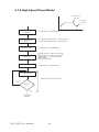
High Speed Preset Model ............................................................ 66
Constant Speed Continuous Mode .............................................. 67
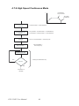
High Speed Continuous Mode .................................................... 68
Constant Speed Origin Return Model ......................................... 69
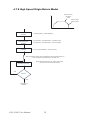
High Speed Origin Return Model ............................................... 70
Appendix A Diagrams ........................................................ 72
A.1 Jumper and Switch Layout ......................................................... 72
A.2 PCI-1243U Block Diagram ........................................................ 73
A.3 Output Circuit Diagram .............................................................. 73
Appendix B Simple St. Motor Driver ............................... 76
Figure B.1:Simple Stepping Motor Driver Block Diagram ........ 76
Figure B.2:Pattern Encoder Connection ...................................... 76
Figure B.3:JP1 at Full Step Control ............................................ 77
Figure B.4:JP1 at Half Step Control ............................................ 78
Figure B.5:4-Phase Stepping Motor Power Control Circuit ....... 79
Appendix C Home Function .............................................. 82
C.1 How to Read the Home Velocity Profile.................................... 82
C.2 Home Mode0
..................... 83
Figure C.1:Velocity Profile of Home Mode0 .............................. 83
C.3 Home Mode1 .............................................................................. 84
Figure C.2:Velocity Profile of Home Mode1 .............................. 84
C.4 Home Mode6 .............................................................................. 85
Figure C.3:Velocity Profile of Home Mode6 .............................. 85
C.5 Home Mode9 .............................................................................. 86
Figure C.4:Velocity Profile of Home Mode9 .............................. 86
vii
PCI-1243U User Manual
viii
CHAPTER
1
2
General Information
If you have just purchased the PCI1243U, or just need to brush up on its
features or specifications, you would
want to read this chapter.
Sections include:
• Introduction
• Features
• Applications
• Specifications
• Block Diagram
Chapter 1 General Information
1.1 Introduction
PCI-1243U is a high-speed four-axis stepping motor control card that
simplifies stepping motor control, giving you added performance from
your stepping motors.
Four-Axis Control
PCI-1243U has one single-chip pulse generator on-board, which enables
the simultaneous and independent control of three axes. PCI-1243U provides digital pulse and directional control (+ and -) for each stepping
motor axis.
User-Friendly Interface
PCI-1243U has been designed to act as a user-friendly solution for your
stepping motor control applications. Programming the PCI-1243U is very
easy. Windows DLL drivers and a utility are provided, and they contain
all the command functions needed for total control of your stepping
motors.
Digital I/O
PCI-1243U features 8 isolated digital inputs and 8 isolated digital outputs
for general I/O use (on/off control etc.).
Isolation Protection
The PCI-1243U's PULSE and DIRECTION outputs and five limits input
switches are isolated from the PC side.
PCI-1243U User Manual
2
1.2 Features
• One on-board pulse generator that enables simultaneous independent
control of four stepping motors
• Two operating modes - two-pulse (+ and - direction pulse) or one-pulse
(pulse-direction) mode
• Programmable step rate from 1 to 400k pps (pulses per second).
• Programmable initial speed, final speed and time duration. Automatic
trapezoidal acceleration/deceleration tamping is performed
16 I/O TTL Compatible Channels
• All inputs/outputs are optically isolated, providing 5000Vrms isolation
protection
• Command Interpreter provided that eases learning the PCI-1243U command set
1.3 Applications
• Precise X-Y-Z position control
• Precise rotation control
• Robotics and assembly equipment
• Other stepping-motor applications
3
Chapter 1
1.4 Specifications
• Number of axes: Three independent axes (individually programmable)
• Operating modes: Two-pulse mode (+ or – direction) or one-pulse
(pulse-direction) mode
• Steps per command: ±16777215 steps
• Step Rate: 1 - 400 kpps
• Acceleration/deceleration ramping: User programmable start, run and
ramping rates.
• Output polarity: Positive/negative going pulse (programmable)
• Output Sink Protection: 1.1 A / all channels
• Output Type: Open Collector, 150 mA/ch, Vmax = 30 V DC
• Limit *5 / EMG *1 / All Isolated / Ref DOC
• Limit switch input voltage: external +12V to +24V
• Limit: ORG/+-SD/+-EL:NC,NO Control By Register
• EMG/Tri-Start: Isolated : NC, NO Control By Jumper
1.4.1 Digital Input / Output
• Input channels: 8 Isolated DI
• Output channels: 8 Isolated open-collector DO
• Input voltage range: DC+12V ~ +24V
• Output capability: Open Collector, 150 mA/ch, Vmax = 30 V DC
1.4.2 General
• Power Consumption:
Normal: 340 mA/ 5 V
Max: 500 mA / 5 V
• Connector: 62-pin D-type connector
• Board Dimensions: 183.5 x 99.06 mm
• Operating Temperature: 0 ~70° C
PCI-1243U User Manual
4
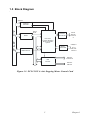
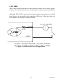
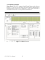
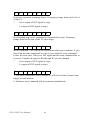
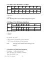
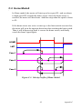
1.5 Block Diagram
Address
Address
Decoder
P
C
B
U
S
DATA
BUS
OUTPUT
ISOLATOR
Buffer
DIR &
PULSE
OUTPUT
S
PCD-4541
2 Phase Stepping
Motor Controller
System
INPUT
ISOLATOR
IRQ Selecteor
ORG,EL+
,
EL- &
SD+,SDINPUTS
DIGITAL
OUTPUTS
DIO
BLOCK
DIGITAL
INPUTS
Figure 1.1: PCI-1243U 4-Axis Stepping Motor Control Card
5
Chapter 1
PCI-1243U User Manual
6
CHAPTER
2
2
Installation
If you have not yet configured and/or
installed your PCI-1243U, or need to
change the configuration this chapter
will give you the information you
require.
Sections include:
• Hardware Installation
• Pin Assignments
• Limit Switch Configuration
• Jumper Settings
• BoardID
Chapter 2 Installation
2.1 Hardware Installation
After you have set the jumpers and BoardID switch, you will be ready to
install the card in your PC's chassis. The following section will assist you
in installing PCI-1243U.
Warning!
Disconnect power from your PC whenever you
install or remove the PCI-1243U or its cables.
2.1.1 Installing the Card in your Computer:
1.
Turn off the computer and all peripheral devices (such as printers
and monitors).
2.
Disconnect the power cord and any other cables from the back of
the computer. Turn the chassis so that the back of the unit faces
you.
3.
Remove the chassis cover (see your computer users guide if necessary).
4.
Locate the expansion slots at the rear of the unit and choose an
unused slot.
5.
Remove the screw that secures the expansion slot cover to the chassis. Save the screw to secure PCI-1243U.
6.
Carefully grasp the upper edge of the PCI-1243U card. Align the
hole in the retaining bracket with the hole on top of the expansion
slot, and align the gold striped edge connector with the expansion
slot socket. Press the board firmly into the socket.
7.
Replace the screw in the expansion slot retaining bracket.
8.
Replace the chassis cover.
9.
Connect the D-62 male connector to the PCI-1243U's 62-pin
female connector. Connect the connector to your stepping motor
driver according to the specifications outlined in Section 2.2.
10.
Connect the cables you removed in step 2. Turn on the computer.
Hardware installation is now complete.
PCI-1243U User Manual
8
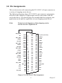
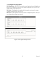
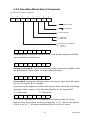
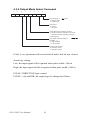
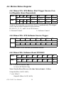
2.2 Pin Assignments
This section assists with connecting the PCI-1243U’s 62-pin connector to
a variety of stepping motor drivers.
The following diagrams shows PCI-1243U’s pin connector assignments,
and offer some examples of input/output circuit connections from the
card to the driver. You should select the example that best supports your
application needs and the capabilities of your stepping motor driver.
Note:
Output circuit diagrams of the stepping motor
can be found in Appendix B
EXT_COM
NC
EXT_GND
AORG
ALCOM
EXT_GND
BORG
BLCOM
EXT_GND
CORG
CLCOM
EXT_GND
DORG
DLCOM
IDO2
IDO5
IDO_COM
NC
IDI2
IDI5
IDI_COM
EMG
ADIR
ALIMASDBDIR
BLIMBSDCDIR
CLIMCSDDDIR
DLIMDSDIDO0
IDO3
IDO6
EXT_GND
IDI0
IDI3
IDI6
NC
1
2
3
4
5
6
7
8
9
10
11
12
13
14
15
16
17
18
19
20
21
22
23
24
25
26
27
28
29
30
31
32
33
34
35
36
37
38
39
40
41
42
43
44
45
46
47
48
49
50
51
52
53
54
55
56
57
58
59
60
61
62
Tri_STA (reversed)
APulse
ALIM+
ASD+
BPulse
BLIM+
BSD+
CPulse
CLIM+
CSD+
DPulse
DLIM+
DSD+
IDO1
IDO4
IDO7
EXT_GND
IDI1
IDI4
IDI7
Figure 2.1: PCI-1243U Pin Assignment
9
Chapter 2
Driving Pins for Each Axis
DIR/-dir
Direction signal output (in direction mode) or (-) direction
pulse output (in pulse mode)
Pulse/+dir
Pulse signal output (in direction mode) or (+) direction
pulse output (in pulse mode)
Emergency Stop Pins
EMG
Emergency Stop input
Tri_STA
Input channel for motion start external trigger signal.
The hardware trigger start function is reserved for future
usage.
EXT_COM
Isolated inputs common point for EMG and Tri_STA
channel
Limit Switch Pins
Lim+
(+) Direction limit switch input
Lim-
(-) Direction limit switch input
SD+
(+) Direction slowdown limit switch input
SD-
(-) Direction slowdown limit switch input
ORG
Original (home) point limit switch input
LCOM
Limit switch common point for each channel
Isolated Digital Input Pins
IDIx
Isolated Digital Input channels, x= 0~7
IDI_COM
Common ground for IDI channels
Isolated Digital Output Pins
IDOx
Isolated Digital Output channels, x=0~7
IDO_COM
Common point for IDO channels
EXT_GND
Ground pin for IDO channels
PCI-1243U User Manual
10
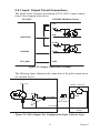
2.2.1 Input / Output Circuit Connections
The figure below illustrates an example of PCI-1243U output connections to the stepping motor driver.
PCI-1243
KR-5MC-5M Motor Driver
+5V
CW+
390 Ohm
CWCW/PULSE
CCW+
390 Ohm
CCW/DIR
CCW-
EXT_GND
GND
Figure 2.2: Output Connections Example
The following figure illustrates the connection of the pulse output pin to
the external device.
IVCC (5V)
Vmax = 30V DC
-
+
V
Load
OUTx/DIRx
Imax= 100mA
EXT_GND
Driver
Figure 2.3: Pulse Output Test Configuration (Open Collector Type)
11
Chapter 2
PCI-1243U provides 8 isolated DI channels and 8 isolated DO channels.
With general purpose I/O points, users can control and monitor peripheral
sensors in their applications. The following figures illustrate how the I/O
points are connected.
V = 12 ~ 24 Vdc
IDI_COM
V
(4.7k)
IDI0 ~ 7
Figure 2.4: Isolated Digital Input Wiring Configuration
IVCC (5V)
Vmax = 30 V DC
IDO_COM
IDO0 ~ 7
+
V
-
Load
EXT_GND
Imax = 200 mA/CH (1.1A/all)
Figure 2.5: Isolated Digital Output Wiring Configuration
PCI-1243U User Manual
12
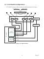
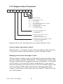
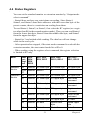
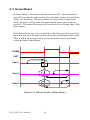
2.3 Limit Switch Configuration)
PCI-1243U features 5 limit switches for additional control of output.
(+)DIRECTION
(-)DIRECTION
TABLE
MOTOR
DRIVER
Lim+
SD+
PCI-1243U
LimINPUT
ISOLATOR
SDORG
DIR
OUTPUT
ISOLATOR
PULSE
Figure 2.6: Limit Switches
13
Chapter 2
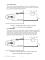
2.3.1 Lim+/ LimThese are the End Limit signal inputs. If there is a signal in the same
direction as the pulse output (in direction or pulse mode) that becomes
active, the pulse output stops immediately.
V = 12 ~ 24 V DC
nLCOM
V
(4.7k)
nLIM+/nLIM-
nLCOM = ALCOM / BLCOM / CLCOM / DLCOM
Figure 2.7: Lim Switch Test Configuration
2.3.2 SD+/SDThese are the Slow-Down signal inputs, which are in operation in the SDenable mode (refer to the control select modes). If there is a signal in the
same direction as the pulse output (in direction or pulse mode) that
becomes active during high-speed start, the frequency ramps down.
When the signal becomes inactive, the frequency ramps up again.
V = 12 ~ 24 V DC
nLCOM
V
(4.7k)
nSD+/nSD-
nLCOM = ALCOM / BLCOM / CLCOM / DLCOM
Figure 2.8: SD Switch Test Configuration
PCI-1243U User Manual
14
2.3.3 ORG
This is the Origin point input. If this signal becomes active during origin
return (refer to the control select modes), pulse output stops immediately.
Although PCI-1243U caters for five limit switches on each axis, not all of
them have to be operated in one application. Refer to following figure for
an example of the usage of limit switches.
V = 12 ~ 24 V DC
nLCOM
V
(4.7k)
nORG
nLCOM = ALCOM / BLCOM / CLCOM / DLCOM
nSwitchIn
= xLIM+
/ xLIM-Test
/ xSD+
/ xSD- / xORG
Figure 2.9:
ORG Switch
Configuration
15
Chapter 2
2.4 Jumper Settings
JP1 has a convenient design that enables storage of motion register
configurations into CPLD, so the configurations can be kept even when
the PC power is off. The factory default is in “Normal” position (1-2 pin
shorted), which means the register setting will disappear after a power
reset. You can move JP1 to the “Keep” position (2-3 pin shorted) to store
configurations.
Table 2.1: JP1 Settings
Normal (reset register) (default).
Keep (store configurations)
JP11 and JP12 set the polarity for Emergency stop and Tri_STA pin
respectively. When the jumper is set to pin 2 and 3 (factory default), the
input channel is in 'normally open'. When the jumper is set to pin 1 and 2,
the input channel is 'normally closed'.
Normally
Closed
V = 12 ~ 24 V DC
EMG/Tri-STA
+
V
Imax = 10 mA
EXT_COM
(4.7k / 1 W)
Normally
Open
Figure 2.10: EMG / Tri_STA Test Configuration
Note:
The factory default is Normally Open.
PCI-1243U User Manual
16
-
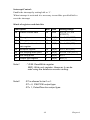
2.5 Setting the BoardID Switch (SW1)
You can use the BoardID command (0x10) to get the board’s unique
identifier. PCI-1243U has a built-in BoardID DIP switch (SW1), which
is used to define each card's unique identifier. You can determine the
identifier in the register as shown in Table 2.2. When there are multiple
cards on the same chassis, this BoardID setting is useful for identifying
each card's device number. We set the PCI-1243U’s BoardID switch to 0
at the factory. If you need to adjust this setting, please see below..
Table 2.2: BoardID Setting (SW1)
BoardID (DEC)
Switch Position
0*
ID3
ON
ID2
ON
ID1
ON
ID0
ON
1
ON
ON
ON
OFF
2
ON
ON
OFF
ON
3
ON
ON
OFF
OFF
4
ON
OFF
ON
ON
5
ON
OFF
ON
OFF
6
ON
OFF
OFF
ON
7
ON
OFF
OFF
OFF
8
OFF
ON
ON
ON
9
OFF
ON
ON
OFF
10
OFF
ON
OFF
ON
11
OFF
ON
OFF
OFF
12
OFF
OFF
ON
ON
13
OFF
OFF
ON
OFF
14
OFF
OFF
OFF
ON
15
OFF
OFF
OFF
OFF
* : Default
2.5.1 BoardID Register
You can determine the BoardID setting in the register as shown below.
Table 2.3: BoardID register of PCI-1243U
Base+(0x10)
3
2
1
0
Abbreviation
ID3
ID2
ID1
ID0
Note:
ID0: The least significant bit (LSB) of BoardID
ID3: The most significant bit (MSB) of BoardID
17
Chapter 2
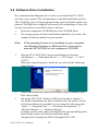
2.6 Software Driver Installation
We recommend installing the driver before you install the PCI-1243U
card into your system. This will guarantee a smooth installation process.
The 32-bit DLL driver Setup program for the card is included on the companion CD-ROM that is shipped with your DAS card package. Please follow the steps below to install the driver software:
1.
Insert the companion CD-ROM into your CD-ROM drive.
2.
The setup program will be launched automatically if you have the
autoplay function enabled on your system.
Note:
If the autoplay function is not enabled on your computer,
use Windows Explorer or Windows Run command to
execute SETUP.EXE on the companion CD-ROM.
3.
Start the PCI-1243U DLL drivers installation by selecting
“Installation” => “Individual Driver” => “PCI Series” => “PCI1243U”.
When the Setup Program is launched, you will see the following
Setup Screen.
4.
Follow the installation instructions step by step to complete your
DLL driver setup.
5.
Set up the PCI-1243U Motion Utility by referring to chapter 3.
For further information on driver-related issues, an online version
of Software Manual is available by accessing the following path:
“Start” => “Program Files” => “Advantech Automation” =>
“Motion Manager” => “Motion Manager”.
Example source codes can be found under the corresponding installation folder such as the default installation path:
\Program Files\Advantech\AMCL\Examples\PCI-1243
PCI-1243U User Manual
18
CHAPTER
3
2
Motion Utility
This chapter introduces the Advantech
Motion Manager utility.
Sections include:
• Introduction
• Configuration
• Motion Operations
Chapter 3 Motion Utility
3.1 Introduction
The Advantech Motion Manager Utility is designed for easy installation,
configuration, and diagnostics on PCI-1243U. In this utility, you can set
mechanical parameters, electrical parameters, and home modes in the
parameter table. Some basic motion functions can also be operated in the
utility, such as point-to-point, continuous movement, and home.
You can also figure the digital input points status easily in the utility. Furthermore, the motion speed profile display function is also implemented
in this software package.
In the following section, all the functions will be introduced one by one.
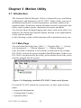
3.1.1 Main Page
You can launch the utility from “Start” => “Program Files” => “Advantech Automation” => “Motion Manager” => “Motion Manager”.
Once the utility is initialed, it will scan the system and list the existing
PCI-1243U cards on the system with their BoardID number. If there is no
PCI-1243U card detected by the utility, please double check if the card is
properly plugged into the system.
Figure 3.1: Displaying Available PCI-1243U Cards on the System
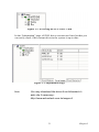
For each PCI-1243U card in the system, there are three main software
pages:
• Inspection (Information)
• Configuration (Config)
• Operation (Run)
PCI-1243U User Manual
20
Figure 3.2: Accessing the PCI-1243U Card
In the “Information” page, all DLL driver versions are listed so that you
can easily check if the current driver in the system is up-to-date.
Figure 3.3: Information Page
Note
You may download the driver from Advantech’s
web site if necessary:
http://www.advantech.com.tw/support/
21
Chapter 3
3.2 Configuration
In the “Configuration” page you can set all the parameters used by PCI1243U, including mechanical, motion I/O and home parameters. You
input the basic mechanical parameters in the first page. This includes
parameters such as maximum RPM of motor, number of pulses per revolution, and the gear ratio of the gear box, if there is one. Then, based on
this mechanical information, the software driver can automatically calculate the unit transformation, so that the user can enjoy the convenience of
inputting commands with Pulse, mm or inch.
PCI-1243U also supports four different types of Home functions, with
related settings that are configurable from this page.
3.2.1 Machine Configuration Page
POLogic: There are two possible logic modes for the pulse output of
PCI-1243U.
Setting Positive Logic means the pulse output channel will normally be in
low status, and the output pulse will start from a rising edge. While the
logic mode is set to Negative Logic, the pulse output channels will normally be high. The choice depends on the type of motor driver.
Pulse Mode: The output of PCI-1243U can be set as CW/CCW mode or
Pulse/Direction mode in this column.
Max Speed (rpm): You need to input the maximum rotation speed of the
motor here. The unit is rpm (revolutions per minute).
PPR (pulse/rev): Property of stepping motor, PPR (pulses per revolution) means the number of pulses that are required to turn the motor one
revolution. With the parameters of maximum speed and PPR, the software driver can calculate the maximum pulse output rate.
Pitch (mm/rev): The property of ball-screws. If ball-screws were used in
the moving table, it is necessary to input the parameter here to use physical units like mm and inch, in the command set.
Gear Ratio: The property of the gear box. If a gear box was used in the
moving table, then it is necessary to input a parameter here to use physical units like mm and inch, in the command set.
PCI-1243U User Manual
22
Figure 3.4: Machine Configuration Page
3.2.2 Motion I/O Configuration Page
HWLimtMode_P: The hardware limitation switch mode in positive
direction. It can be “Normal Open” or “Normal Close”.
HWLimtMode_N: The hardware limitation switch mode in negative
direction. It can be “Normal Open” or “Normal Close”.
SD_P: The “Slow-Down” switch can be enabled by checking the dialog
box above. And Users can set the hardware slow-down switch mode in
positive direction as “Normal Open” or “Normal Close” in this column.
SD_N: The hardware slow-down switch mode in negative direction. It
can be “Normal Open” or “Normal Close”.
Figure 3.5: Motion I/O Configuration
23
Chapter 3
3.2.3 Home Configuration Page
Home Mode: PCI-1243U supports four different Home modes, they are
mode0, 1, 6, and 9. Choose the most suitable mode to get better homing
accuracy. Please refer to Appendix C for detailed information on each
Home mode.
Direction: This defines the initial direction when the homing movement
starts. As long as the direction is defined, the motor will move in the specific direction. It will stop when it reaches the ORG sensor, or return if
the limit switch was reached first.
ORG Mode: The hardware ORG sensor switch mode in original point. It
can be “Normal Open” or “Normal Close”.
Reset Mode: While the setting is “Reset Counter”, the counter value will
be reset after homing is accomplished. If the “Do not reset counter” mode
was chosen, the counter value will stay as it was, even when the homing
process is finished.
SV: The start up speed while homing.
DV: The final drive speed while homing.
Acc. Time: The time period for acceleration from “SV” to “DV”.
Offset: The additional offset distance after reaching the original point.
Unit: The unit of above commands can be pulse, mm or inch.
Figure 3.6: Home Configuration
Apply, Save and Load the parameters:
PCI-1243U User Manual
24
After finishing the configuration for each axis, the parameters can be
applied to the PCI-1243U card by using “Apply to Axis” as shown in the
following diagram.
You can also press the “New” button to create a virtual PCI-1243U, and
simulate the parameters.
The parameters can be saved into a file and loaded from a file. This
makes it possible to send the configuration file to a remote site by e-mail,
so several sites can easily have the same configuration.
Figure 3.7: Save and Load Configuration Files
3.3 Motion Operations
3.3.1 Testing Motion Movement
The motion utility provides operational functions as well as configuration
functions. You can test motion movement without writing any software
program. However, please do apply the parameters you set for the axes in
the configuration pages. Since the default parameters are all "0", if you
did not press the "Apply to Axis" button, operation of the axes is not possible and there will be a red cross on the tab as shown below.
25
Chapter 3
3.3.2 Point to Point Movement
Acc/Dec Mode: PCI-1243U supports Trapezoid and S-curve acceleration/deceleration modes. The mode can be set in the column.
AccTime_L: Acceleration time period allowed in Trapezoid acceleration
mode.
DecTime_L: Deceleration time period allowed in Trapezoid deceleration
mode.
AccTime_S: Acceleration time period allowed in S-curve acceleration
mode.
DecTime_S: Deceleration time period allowed in S-curve deceleration
mode.
SV: Start-up velocity of the movement
DV: Final driving velocity of the movement
Unit: The unit of above commands can be pulse, mm or inch.
Distance: The distance you want to move in the point to point movement.
PtP ABS: In a Point to Point movement, the ‘Distance’ mentioned above
is calculated on the basis of an absolute coordinate system. That means
the distance is from the original starting point.
PtP INC: In Point to Point movement, the ‘Distance’ mentioned above is
calculated on the basis of a relative coordinate system. That means the
distance is from the current location.
CW: In continuous movement, press the CW button to make the motor
turn clockwise.
CCW: In continuous movement, press the CCW button to make the
motor turn counterclockwise.
Stop_S: Once this button is pressed, the motor will decelerate to SV then
stop.
Stop_M: When the button is pressed the motor will stop immediately.
Change DV: This is an advanced function of PCI-1243U that can change
speed on the fly. DV can be changed directly without decelerating to initial speed.
Hold: The movement can be paused by pressing the “Hold” button.
Conti.: When movement is paused by the “Hold” command, you can
resume movement by pressing the “Conti.” button.
PCI-1243U User Manual
26
Figure 3.8: Point to Point Movement
27
Chapter 3
3.3.3 Home Function
Home Mode: PCI-1243U supports four different Home modes, they are
mode0, 1, 6, and 9. Users can choose the best fit mode to get the proper
homing accuracy. Please refer to Appendix C for the detail definition of
each Home mode, and 3.2.3 for parameter information.
.
Figure 3.9: Home Function
PCI-1243U User Manual
28
3.3.4 Digital I/O Operation
DO Mask State: PCI-1243U provides a mask option for each digital output bit. If the mask bit is not set, the output command will not affect the
output status of the specific bit.
DO State: Checking the box under the bit number can issue the status
change command to the specific bit.
DI State: In this column it shows the status of digital input bits, and you
can change the polling time interval.
Figure 3.10: Digital I/O Operation
29
Chapter 3
PCI-1243U User Manual
30
CHAPTER
4
2
Register Programming
This chapter describes the PCI-1243U's
hardware registers. It also contains typical operational procedures that will
assist you in program design. This
chapter is a good place to start getting
to know and use the capabilities of the
PCI-1243U to best suit your application.
Sections include:
• PCI-1243U Registers
• Programming PCI-1243U
• Command Modes
• Status Registers
• General I/O Registers
• Motion Status Register
• Typical Operational Procedures
Chapter 4 Register Programming
4.1 Motion Control Registers
Several motion control registers are used to control PCI-1243U. These
registers are used to store commands, speed, mode, number of pulses and
more. The following sections describe these registers in detail.
4.1.1 R0: Preset Pulse Counter (24 bits)
PCI-1243U has an internal preset countdown counter. By entering a number of pulses, this preset counter will begin counting down from that
point.
The preset counter decrements by one for each pulse output in the continuous, zero return and preset operations. However, if the preset counter
operation mode is inhibited by the output mode command, the preset
counter will not count down.
The counter value (number of remaining pulses) can be read while in
operation or while stopped. To read the value, first select R0. The register
select timing latches the data into a 24-bit read buffer.
In preset operation, PCI-1243U places a number of positioning pulses in
this register, and then starts the operation. Once the operation has started,
the counter value is decremented with each pulse that is output. When the
number of pulses that have been output is equal to the value originally
entered in the preset counter, the value in the counter will be zero and
PCI-1243U will stop operation.
The allowable range is 0 to 16,777,215 (FFFFFF HEX).
If you enter 0 in the preset counter and write the start command, PCI1243U will not use the preset operation. When INT output is enabled,
PCI-1243U will output an INT signal.
If you stop the preset operation using the stop command or an external
signal, the number of remaining pulses will be saved in the preset
counter. By entering a new start command, PCI-1243U will continue to
output all of the remaining pulses.
After the preset number of pulses has been output, the value in the preset
counter will be 0.
If you want to restart the operation using the same number of pulses, you
will have to put the value in R0 again.
PCI-1243U User Manual
32
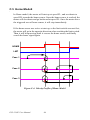
4.1.2 R1: FL Speed Register (13 bits)
This register is used to set the FL (initial/low) speed. To operate in high
speed mode, PCI-1243U will start with the FL speed and then accelerate
to the FH (final/high) speed. If a deceleration-stop command is entered
during high-speed operation, PCI-1243U will decelerate. When the speed
drops to FL speed, the operation will stop.
If the FL speed is set to 0, the motor may not actually stop. Make sure to
set the FL speed to a number greater than 1.
The allowable range is 1 to 8,191 (1FFF HEX).
The relationship between the value entered and the output pulse speed
varies with the value placed in R4 (Please refer to 4.1.5).
4.1.3 R2: FH Speed Register (13 bits)
This register is used to set the FH (final/high) speed.
The allowable range is 1 to 8,191 (1FFF HEX).
The relationship between the value entered and the output pulse speed
varies with the value placed in R4 (Please refer to 4.1.5).
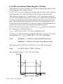
Speed
Speed
FH
FH
FL
FL
High
Speed
Start
time
time
Deceleration
stop input
Figure 4.1: R4’s Effect on Output Pulse Speed
33
Chapter 4
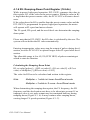
4.1.4 R3: Accel/decel Rate Register (10 bits)
This register is used to select the acceleration (ramping up) and deceleration (ramping down) characteristics.
If PCI-1243U executes a high-speed mode start, the motor starts at the FL
speed entered in R1, and accelerates to the FH speed entered in R2.
The motor decelerates to FL speed when a “SD” (slow down) signal is
received, the ramping down point is reached, or a deceleration command
is received. Specify the acceleration and deceleration characteristics for
these operating patterns using the accel/decel rate setting register. The
acceleration rate of the linear accel/decel is equal to the maximum acceleration rate of the S-curve acceleration/deceleration pattern.
If the reference clock period is (TCLK) [sec], TSUD (the time required for
the ramping-up / ramping-down) is:
TSUD = [(R2)-(R1)] x (R3) x (TCLK) x Multiplier [sec]
Alternatively, if the ramping-up/ramping-down time is known, R3 can be
calculated as: R3 = TSUD / {[(R2)-(R1)] x (TCLK) x Multiplier}
Note
Multiplier = 1 while in Linear Accel/Decel mode
Multiplier = 2 while in S-curve Accel/Decel mode
The range for R3 is 002 (hex) to 3FF (hex) (2 to 1023 in decimal).
Note
For PCI-1243U, TCLK = 233.ns
The allowable range is: 2 to 1,023 (3FF HEX).
Speed
FH
FL
TSUD
TSUD
Figure 4.2: R3’s Effect
PCI-1243U User Manual
34
time
4.1.5 R4: Multiplier Register (10 bits)
The speed setting registers R1 and R2 can have values from 1 to 8,191.
The relationship between the values entered and the output pulse speed
can be set using this multiplier register.
When a set value on the speed register is Rf (where Rf is a value set at R1
and R2), the frequency outputted at the PULSE OUTPUT terminal
FPOUT is
FPOUT = {(Reference clock freq. [Hz] x (Rf)) / (8192 x (R4)}
= (Rf) x {(Reference clock freq.) / [8192 x (R4)]}
When (reference clock)/ [8192 x (R4)]= 1 ... 1x mode
When (reference clock)/ [8192 x (R4)]= 2 ... 2x mode
For PCI-1243U, the reference clock frequency is 4.9152 [MHz], Therefore:
(R4)= 600 (=258 hex) 1x mode
(R4)= 300 (=12C hex) 2x mode
The setting range is 002 (hex) to 3FF (hex), which corresponds to 2 to
1023 in decimal notation. The smaller the setting value, the higher the
output frequency.
35
Chapter 4
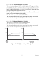
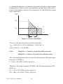
4.1.6 R5: Ramping-Down Point Register (16 bits)
While in preset, high-speed operation, PCI-1243U compares the value in
this register, R5, to the value in the preset counter. When the value in R5
is larger than the preset counter value, the PCI-1243U will start to decelerate.
If the value placed in R5 is smaller than the preset counter value and the
PCI-1243U is programmed for preset, high-speed operation, the motor
will operate at FL speed and not accelerate.
The FL speed, FH speed, and the accel/decel rate determine the rampingdown point.
Please note that in PCI-1243U, the R5 value is calculated by the user. The
system will not define the R5 value automatically.
Entering inappropriate values may stop the output of pulses during deceleration, or cause PCI-1243U to operate longer at the FL speed after deceleration.
The allowable range is 0 to 65,535 (FFFF HEX) of pulses remaining at
which to start deceleration.
Calculating the Ramping-Down Point
R5 set value [pulses] = {[(R2 set value)2 - (R1 set value)2] x (R3 set
value) x Multiplier} / [(R4 set value) x 8192]
The value for R5 has to be calculated and written in the register.
Note
Multiplier = 1 while in Linear Accel/Decel mode
Multiplier = 2 while in S-curve Accel/Decel mode
When determining the ramping-down point, the FL frequency, the FH
frequency and the deceleration rate have to be taken into account. If an
improper value is set, pulse output may be terminated halfway during
ramping-down (Figure 4.3. A) or may continue after ramping-down,
causing longer FL speed operation (Figure 4.3. C).
PCI-1243U User Manual
36
Speed
FH
R5 setting value is
too small
FL
A
time
Speed
FH
R5 setting value is optimal
(several pulses at FL)
FL
B
time
Speed
FH
R5 setting value is
too large
FL
C
time
Figure 4.3: Setting the Ideal Ramping-Down Point
37
Chapter 4
A ramping-down point is set based on the number of pulses output during
ramping-down. Therefore the area marked by oblique lines in the chart
below is the number of pulses to be calculated. FL and FH are the output
pulse frequencies.
PPS
A
FH
F
FL
E
D
t
B
Ts d
C
Figure 4.4: Pulse Calculation
TSD [sec], the time required for the deceleration is:
TSD = [(R2)-(R1)] x (R3) x Multiplier / (CLOCK) (1)
where CLOCK = 4.9152 MHz
Note
Multiplier = 1 while in Linear Accel/Decel mode
Multiplier = 2 while in S-curve Accel/Decel mode
The relationship between the set value on speed register (Rf) and output
frequency (F [PPS]) is
F = (Rf) x (CLOCK)/ [8192 x (R4)] (2)
Therefore, FL output frequency FL [PPS] and FH output frequency FH
[PPS] are
FL = (R1) x (CLOCK)/ [8192 x (R4)] (3)
FH = (R2) x (CLOCK)/ [8192 x (R4)] (4)
PCI-1243U User Manual
38
PSD, the number of pulses during T, [sec] is represented by the area of the
trapezoid A-B-C-F
PSD = {[(FL) + (FH)]* Ted}/ 2(5)
Substitute equations (1), (3) and (4) into equation (5)
PSD = {[(R2)^2 – (R1)^2] x (R3) x Multiplier} / [2 x 8192 x (R4)]
When output 5 pulses at FL speed after the completion of the rampingdown, the set value of the ramping-down point register (R5) is
R5 = PSD + 5
R5 = {[(R2)^2 – (R1)^2] x (R3) x Multiplier} / [16384 x (R4)] + 5
Note
Multiplier = 1 while in Linear Accel/Decel mode
Multiplier = 2 while in S-curve Accel/Decel mode
4.1.7 R6: Idling Pulse Register (3-bit)
To operate in high speed mode, the motor is accelerated quickly after
starting. Therefore, the speed calculated from the output pulse frequency
will be higher than the FL speed that is set. If FL is set to a value lower
than the self-start frequency, the motor will not start.
Therefore, in order to be able to start from near the self-start frequency,
the acceleration using the FL speed can be started from 1 to 7 pulses after
the start command. The pulses that the start is delayed by are referred to
as idling pulses.
The allowable range is 0 to 7. This is effective in high-speed operation.
Setting this register to 0 will provide a normal start.
4.1.8 R7: Environmental Data Register (1-bit)
The allowable range is 0 or 1
0CW/CCW pulse type
1Pulse/DIR type
39
Chapter 4
4.2 Programming PCI-1243U
PCI-1243U stores a selected command in a buffer. This command
remains there until a new command is received. The only command that
can be RESET, is the 'starting mode' command.
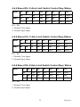
4.2.1 I/O Control Register Map:
The following table depicts the PCI-1243U’s register I/O address map.
Axis
Offset
Address
R/W
Definition
X
(0)
0x00
Write
Command Buffer
Read
Status0
0x01
0x02
0x03
Y
(1)
0x04
0x05
0x06
0x07
PCI-1243U User Manual
Write
Data Register (LowerBit7 To Bit0)
Read
Internal Data (Lower)
Write
Data Register (MiddleBit15 To Bit8)
Read
Internal Data (Middle)
Write
Data Register (UpperBit23 To Bit16)
Read
Internal Data (Upper)
Write
Command Buffer
Read
Status0
Write
Data Register (LowerBit7 To Bit0)
Read
Internal Data (Lower)
Write
Data Register (MiddleBit15 To Bit8)
Read
Internal Data (Middle)
Write
Data Register (UpperBit23 To Bit16)
Read
Internal Data (Upper)
40
Z
(2)
0x08
0x09
0x0A
0x0B
U
(3)
0x0C
0x0D
0x0E
0x0F
0x10
0x11
0x12
0x13
0x14
0x15
0x16
0x17
Write
Command Buffer
Read
Status0
Write
Data Register (LowerBit7 To Bit0)
Read
Internal Data (Lower)
Write
Data Register (MiddleBit15 To Bit8)
Read
Internal Data (Middle)
Write
Data Register (UpperBit23 To Bit16)
Read
Internal Data (Upper)
Write
Command Buffer
Read
Status0
Write
Data Register (LowerBit7 To Bit0)
Read
Internal Data (Lower)
Write
Data Register (MiddleBit15 To Bit8)
Read
Internal Data (Middle)
Write
Data Register (UpperBit23 To Bit16)
Read
Internal Data (Upper)
Write
NA
Read
Board ID (Version Code)
Write
IDO Port (D7~ D0)
Read
Read Back IDO Setting
Write
NA
Read
IDI Port (D7 ~ D0)
Write
IDI Control REG
Read
IDI Control REG
Write
IRQ Control REG_L
Read
IRQ Status_L(Reset Status)
Write
IRQ Control REG_H
Read
IRQ Status_H (Reset Status)
Write
X
Read
IRQ Status_L
Write
X
Read
IRQ Status_H
41
Chapter 4
0x18
0x19
0x1A
0x1B
0x1C
0x1D
0x1E
0x1F
0x20
0x21
0x22
0x23
0x24
Write
Counter Data REG_L
Read
Counter Data REG_L
Write
Counter Data REG_H
Read
Counter Data REG_H
Write
Counter Control REG
Read
Counter Control REG
Write
Load Counter Data
Read
X
Write
STA_Mode
Read
STA_Mode Status
Write
SW STA Trigger
Read
NA
Write
Reset PCD4541 Command
Read
NA
Write
NA
Read
NA
Write
X-Axis Limit Switch Control Register
Read
X-Axis Limit Switch Control Status
Write
Y-Axis Limit Switch Control Register
Read
Y-Axis Limit Switch Control Status
Write
Z-Axis Limit Switch Control Register
Read
Z-Axis Limit Switch Control Status
Write
U-Axis Limit Switch Control Register
Read
U-Axis Limit Switch Control Status
Write
NA
Read
Limit switch status
For each motion axis, four register addresses are used. One command
buffer and three data buffers.
PCI-1243U User Manual
42
Command Buffers: WR0, WR4, WR8 and WR12
Each of the three channels has a command buffer which enables individual programming. Channel l's command buffer is BASE + 0, Channel 2's
is BASE + 4, Channel 3's is BASE + 8 and Channel 4's is BASE + 12. A
command can be written to any of the three buffers, and the appropriate
channel will respond to the command.
Low Data Buffers: WR1, WR5, WR9 and WR13
Low data-buffer for each channel is found at BASE + 1, BASE + 5,
BASE + 9 and BASE + 13, for channel 1, channel 2, channel 3 and channel 4 respectively. During writing (output), these buffers contain data bits
0-7 of the respective channels.
Middle Data Buffers: WR2, WR6, WR10 and WR14
Middle data-buffer for each channel is found at BASE +2, BASE +6,
BASE +10 and BASE +14, for channel 1, channel 2, channel 3 and channel 4 respectively. When writing (output), these buffers contain data bits
8-15 of the respective channels.
High Data Buffers: WR3, WR4, WR11 and WR15
High data-buffer for each channel is found at BASE +3, BASE +7, BASE
+11 and BASE +15, for channel 1, channel 2, channel 3 and channel 4
respectively. When writing (output), these buffers contain data bits 16 -23
of the respective channels.
43
Chapter 4
4.2.2 Command Buffer Register Format
The command buffer register format is as follows:
Register format
D7
D6
C1
C0
Mode
D5
D4
D3
D2
D1
D0
Command
Selection Modes
The two high-order bits of the command buffer specifies the command
that will be executed. The remaining six bits contain command parameters. The command modes available are as follows:
Selection modes
C1
C0
0
0
Start-Stop Command selection
0
1
Operation Mode Select command
1
0
Register Select command
1
1
Output Mode select command
Please refer to section 4.3 for details on each command mode.
PCI-1243U User Manual
44
4.3 Command Modes
The following sections describe all the available commands and their
parameters in detail.
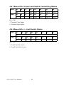
4.3.1 Start-Stop Commands
7
6
0
5
4
3
2
1
0
0
Frequency Selection
0: Use FL frequency
1: Use FH frequency
External start control
0: Do not inhibit a start
1: Inhibit the start command
(till trigger)
0: Constant speed mode
1: High Speed mode
1: Start/stop control
0: Stop interrupt reset
1: Stop interrupt enable
0
0
*
1
0
0
0
0
Constant speed operation with the FL register. Operates at the speed set
for the FL register.
0
0
*
1
0
0
0
1
Constant speed operation with the FH register. Operates at the speed set
for the FH register.
0
0
*
1
0
1
0
1
High speed mode operation with the FH register. Frequency ramps up
halfway from the rate of FL to that of FH. During high-speed start this
command lets the frequency ramp up/down to the rate of the FH speed.
45
Chapter 4
0
0
*
1
0
1
0
0
Dual rate operation (ramping down). Frequency ramps down to the level
of the FL.
*
0 (no output of INT signal at stop)
1 (output of INT signal at stop)
0
0
*
1
1
1
0
0
Decelerating stop (reset command is required after stop). Frequency
ramps down to the rate of the FL, then stops.
0
0
0
0
1
0
0
0
Reset command. This stops pulse generation under any condition. If you
start with the start-command, be sure to reset with the reset command
before the next start. This gives INT signal and the start command has to
be reset. Contents in registers R0 through R7 are not changed.
*
0 (no output of INT signal at stop)
1 (output of INT signal at stop)
0
0
0
0
0
0
1
0
1: The start command is set to standby. It will wait for the external start
trigger to start motion.
0: Software start command will start motion immideately.
PCI-1243U User Manual
46
4.3.2 Operation Mode Select Command
Operation Mode Select Command
7
6
0
5
4
1
3
2
1
0
0
1: ORG signal enable
1: SD+ signal enable
1: Preset enable
0: (+)direction
1: (-)direction
Accel/decal characteristic
0 : Linear
1 : S-curve
0
1
0
0
*
0
0
:
0
Manual mode. Operation initiated in the start mode continues until the
stop command is transferred.
0
1
0
0
*
0
0
1
Origin return mode. Operation initiated in the start mode continues until
the mechanical origin signal or stop command comes.
0
1
0
0
*
1
0
0
Preset mode. Operation initiated in the start mode, stops when the quantity set for register R0 is reached.
Operation in the high speed start mode ramps down when the remaining
quantity of the counter is less than the quantity set for register R5.
0 (+) direction
0
1
*
1 (-) direction
0
0
0
0
0
PCI-1243U supports two acceleration/deceleration modes. You can
choose linear accel/decal mode by setting bit5 as ‘0’. On the other hand,
if bit6 is set to ‘1’, then the acdel/decal profile will be S-curve.
47
Chapter 4
4.3.3 Register Select Command
7
6
1
0
5
4
3
2
1
0
Register Selection
0
0
0
0
1
1
1
1
0
0
1
1
0
0
1
1
0
1
0
1
0
1
0
1
R0: Preset Counter Data
R1: FL register
R2: FH register
R3: Acceleration/deceleration rate register
R4: Multiplier register
R5: Ramping-down point register
R6: Set idling pulse
R7: Output type register
Preset counter operation control
0 Counts output pulse
1 Do not count
Ramping-down point interrupt control
0 Ramping-down reset
1 Ramping-down interrupt enable
Interrupt output when external start is enabled
0 : Interrupt is not output (reset)
1 : Interrupt is enabled
:
Register select code: Selecting an access register with last 3 bits.
Preset Counter Operation Control:
When this bit is 1, the preset counter will stop counting. When this bit is
0, the preset counter will decrement by one for each pulse output.
Ramping-down Point Interrupt Control:
This bit controls whether or not the INT signal is output when the ramping-down point is reached. When this bit is 1 and the preset counter value
becomes smaller than the ramping-down point setting in R5, it will output
an INT signal. To reset the INT signal, set this bit to 0. If you want to
mask this operation, leave this bit set to 0. The INT terminal output is the
result of an logical OR of this signal with the interrupt signal when
stopped. To determine which source has caused the INT signal to be output, check Status0.
PCI-1243U User Manual
48
Interrupt Control:
Enable the interrupt by setting bit0 as ‘1’.
When interrupt is activated it is necessary to read this specified bit0 to
reset the interrupt.
Kinds of registers and data bits
Description
Bits
R/W
Setting Range
R0
Preset counter data
24
R/W
0 to 16,777,215
(FFFFFF)
R1
FL register
13
W(R)
1 to 8,191 (1FFF)
R2
FH register
13
W(R)
1 to 8, 191 (1FFF)
R3
Acceleration/deceleration
rate register
10
W(R)
2 to 1, 023 (3FF)
R4
Multiplier register
10
W(R)
2 to 1, 023 (3FF)
R5
Set ramping-down point
16
W(R)
0 to 65, 535 (FFFF)
R6
Set idling pulse
3
W(R)
0 to 7
R7
Output type register
1
W(R)
0 to (1)
Note1
: * R/W: Read/Write register
W(R): Write only register. However, it can be
read using the extension monitor setting.
Note2
R7 is allowed to be 0 or 1.
R7 = 0, CW/CCW output type
R7= 1, Pulse/Direction output type
49
Chapter 4
4.3.4 Output Mode Select Command
7
6
1
1
5
4
3
2
1
0
0
Logic setting of +/0: Negative logic
1: Positive logic
PO output
Pulse output
0: Output
1: No output
Intermediate stop accel/decel operation
0: Enable accel/decel operation (continuous)
1: Disable accel/decel operation (change to
constant speed)
Input signal sensitivity setting for
and EMG (*)
0: High sensitivity
1: Low sensitivity
ORG , EL
Monitor mode selection
0: Standard monitor
1: Extension monitor
If bit3 is set, operations will not accel/decal unless this bit was cleared.
Sensitivity setting:
Low: the input signal will be ignored when pulse width < 800 ns
High: the input signal will be recognized when pulse width < 800 ns
PULSE / DIRECTION logic control
PULSE / +dir and DIR/-dir output logic be changed as follows
PCI-1243U User Manual
50
4.4 Status Registers
You can set the standard monitor or extension monitor by “Output mode
select command”
- Status0 does not have any restrictions on reading. Since Status1,
Status2, and Status3 share their addresses with the lower data byte of the
preset counter, there is a restriction on reading from them.
To read Status1, Status2, or Status3, first select the R7 register (or a register other than R0 in the normal monitor mode). Then you can read Status1
from the lower data byte, Status2 from the middle data byte, and Status3
from the upper data byte.
- Status0 to 3 are latched while reading. The data bus will not change
while in the read cycle.
- After operation has stopped, if the start mode command is read with the
extension monitor, the start control mode bit will be 0.
- When reading using the register select command, the register selection
is limited to R3 only.
Mode
Addr
ess\
Regi
ster
RD0,
RD4,
RD8,
RD12
Standard
Monitor
R0
Status0 R0 lower byte R0 middle byte
R0 upper byte
R1 to
R7
Status0 Status1
0
Extension R0
Monitor
R1
RD1, RD5,
RD9, RD13
RD2, RD6,
RD10, RD14
0
RD3, RD7,
RD11, RD15
Status0 R0 lower byte R0 middle byte
R0 upper byte
Status0 R1 lower byte R1 upper byte
Start mode
command
R2
Status0 R2 lower byte R2 upper byte
Control mode
command
R3
Status0 R3 lower byte R3 upper byte
Register select
command
R4
Status0 R4 lower byte R4 upper byte
Output mode
command
R5
Status0 R5 lower byte R5 upper byte
R7 data
R6
Status0 R6 data
Speed lower
byte
Speed upper
byte
R7
Status0 Status1
Status2
Status3
51
Chapter 4
The definitions of Status registers are as following:
4.4.1 Status0: Channel Status Buffers (RD0, RD4, RD8
and RD13)
There is a status buffer for each channel (status 0). These buffers are
found at BASE +0, BASE +4, BASE +8 and BASE +13 for channel 1,
channel 2, channel 3 and channel 4 respectively. These buffers enable
you to read the internal status of each channel, and also get certain information on input signals or conditions.
7
6
5
4
3
2
1
0
Monitor INT output when operation is stopped
0: INT is being output
Monitor INT output at ramping-down point
0: INT is being output
Monitor INT output at external start
0: INT is being output
Operation status
0: Stopped
1: Operating
Pulse output zero status
0: Non zero
1: Zero
Pulse counter and R5 comparison
0: Pulse counter > R5
1: Pulse counter <= R5
Monitor acceleration status
0: Not accelerating
1: Accelerating
Monitor deceleration status
0: Not decelerating
1: Decelerating
Status 0 bit configuration
4.4.2 Extension Monitor
When the Extension Monitor was selected, you can check the value of
each register R0 ~ R7 by assigning the register with “register selection
command”, and then read the specific address respectively. Also, Status1,
Status2 and Status3 can be read in the extension monitor mode. On the
following page are the definitions of each status register.
PCI-1243U User Manual
52
7
6
5
4
3
2
1
0
Monitor -EL terminal
0: Off
1: On
Monitor +EL terminal
0: Off
1: On
Monitor ORG terminal
0: Off
1: On
NA
NA
Monitor -SD terminal
0: Off
1: On
Monitor +SD terminal
0: Off
1: On
NA
Status 1 bit configuration
7
6
5
4
3
2
1
0
NA
NA
NA
NA
Monitor -PO terminal
0: Off
1: On
Monitor +PO terminal
0: Off
1: On
NA
Monitor interrupt (each axis)
0: No interrupt,
1: Interrupt occurred
For the value of Status3, it should be “0100-0000”. It represents the
PCD4541 chipset.
53
Chapter 4
4.5 General I/O Registers
Register from Base+10h to Base+1Bh are for general I/O, following are
the definitions of each register.
4.5.1 Base+10h: Read Board ID
Write D7
Read
D6
D5
D4
D3
D2
D1
D0
-
-
-
-
-
-
-
-
D7
D6
D5
D4
D3
D2
D1
D0
-
-
-
-
ID3
ID2
ID1
ID0
This Register Is Read Board ID (D3~D0)
The Operation Steps are as the following
Step 1: outportb (base+0x10, 0x00)
Step 2: BoardID = inportb (base+0x10)
4.5.2 Base+11h: Read/Write IDO Port
Write
Read
D7
D6
D5
D4
D3
D2
D1
D0
IDO7
IDO6
IDO5
IDO4
IDO3
IDO2
IDO1
IDO0
D7
D6
D5
D4
D3
D2
D1
D0
IDO7
IDO6
IDO5
IDO4
IDO3
IDO2
IDO1
IDO0
This Register Is Read/Write IDO Output (D7~D0)
4.5.3 Base+12h: Read/Write IDI Port
Write
Read
D7
D6
D5
D4
D3
D2
D1
D0
-
-
-
-
-
-
-
-
D7
D6
D5
D4
D3
D2
D1
D0
IDI7
IDI6
IDI5
IDI4
IDI3
IDI2
IDI1
IDI0
This Register Read IDI Port (D7~D0)
PCI-1243U User Manual
54
4.5.4 Base+13h: R/W IDI Port Trigger Control Register
Write D7
D6
D5
D4
D3
D2
D1
D0
IDI_Ctl7 IDI_Ctl6 IDI_Ctl5 IDI_Ctl4 IDI_Ctl3 IDI_Ctl2 IDI_Ctl1 IDI_Ctl0
Read D7
D6
D5
D4
D3
D2
D1
D0
IDI_Ctl7 IDI_Ctl6 IDI_Ctl5 IDI_Ctl4 IDI_Ctl3 IDI_Ctl2 IDI_Ctl1 IDI_Ctl0
IDI_Ctl7 ~ IDI_Ctl0: Isolated Digital Input channel interrupt Edge Trigger Control
0: IDIx (x = 7 ~ 0): Falling Edge Trigger
1: IDIx (x = 7 ~ 0): Rising Edge Trigger
4.5.5 Base+14h: IRQ Control/Enable Register Low Byte
Write D7
D6
D5
D4
D3
D2
D1
D0
INT_IDI7 INT_IDI6 INT_IDI5 INT_IDI4 INT_IDI3 INT_IDI2 INT_IDI1 INT_IDI0
Read D7
D6
D5
D4
D3
D2
D1
D0
INT_IDI7 INT_IDI6 INT_IDI5 INT_IDI4 INT_IDI3 INT_IDI2 INT_IDI1 INT_IDI0
INT_IDI7~ INT_IDI0:
0: Disable IDIx INT (x = 7 ~ 0)
1: Enable IDIx INT (x = 7 ~ 0)
4.5.6 Base+15h: IRQ Control/Enable Register High Byte
Write
Read
D7
D6
D5
D4
D3
D2
D1
D0
INT_All
-
-
-
-
-
INT_Motion
INT_Timer
D7
D6
D5
D4
D3
D2
D1
D0
INT_All
-
-
-
-
-
INT_Motion
INT_Timer
INT_All:
0: Disable INT of all channels
1: Enable INT of all channels
INT_Motion, INT_Timer:
0: Disable INT for Motion or Timer functions
1: Enable INT for Motion or Timer functions
55
Chapter 4
4.5.7 Base+16h: IRQ Status Low Byte
Write
D7
D6
D5
D4
D3
D2
D1
D4
D3
D2
D1
D0
Clear interrupt flag
Read
D7
D6
D5
D0
IDI_Sta7 IDI_Sta6 IDI_Sta5 IDI_Sta4 IDI_Sta3 IDI_Sta2 IDI_Sta1
IDI_Sta0
IDI_Sta7~ IDI_Sta0: IDIx (x = 7 ~ 0) INT Status
0: In-Active
1: Active
Note: This flag will be cleared while writing to the register
4.5.8 Base+17h: IRQ Status High Byte
Write
D7
D6
D5
D4
D3
D2
D1
D0
Clear interrupt flag
Read
D7
D6
D5
D4
D3
D2
D1
D0
Sta_All
-
-
-
-
-
Sta_Motion
Sta_Timer
Sta_All: INT Status
0: Inactive
1: Active
Sta_Motion, Sta_Timer:
0: INT is inactive for Motion or Timer functions
1: INT is active for Motion or Timer functions
Note
This flag will be cleared while writing to the
register
4.5.9 Timer Function Specification
Clock Base : 1 MHz On Board OSC
Timer Tick Base: 10 Clock Base (100 kHz)
Timer Tick Width: 10 µs
PCI-1243U User Manual
56
4.5.10 Base+18h: Counter Data Register Low byte
Write
D7
D6
D5
D4
D3
D2
D1
D0
D3
D2
D1
D0
Counter DATA (Low Byte)
Read
D7
D6
D5
D4
Counter DATA (Low Byte)
4.5.11 Base+19h: Counter Data Register High Byte
Write
D7
D6
D5
D4
D3
D2
D1
D0
D3
D2
D1
D0
Counter DATA (High Byte)
Read
D7
D6
D5
D4
Counter DATA (High Byte)
4.5.12 Base+1Ah: Counter Gate Control Register
Write
Read
D7
D6
D5
D4
D3
D2
D1
D0
-
-
-
-
-
-
-
CNT_EN
D7
D6
D5
D4
D3
D2
D1
D0
-
-
-
-
-
-
-
CNT_EN
CNT_EN: Counter Gate Control status
0: Disable
1: Enable
4.5.13 Base+1Bh: Counter Load Trigger
Write
D7
D6
D5
D4
D3
D2
D1
D0
D2
D1
D0
Load counter setting value into chip
Read
D7
D6
D5
D4
D3
X
57
Chapter 4
4.6 Motion Status Register
4.6.1 Base+1Ch: STA Motion Start Trigger Source Control Register (Axes Dependant)
Write
D7
D6
D5
D4
NA
Read
D3
D2
D1
D0
U-Axes
Z-Axes
Y-Axes
X-Axes
D7
D6
D5
D4
D3
D2
D1
D0
0
0
0
0
U-Axes
Z-Axes
Y-Axes
X-Axes
With the STA function, you can start all axes synchronously. The trigger
source can be either external or from software.
D3~D0: X-, Y-, Z-, and U-Axis STA Source
0: External Control
1: Software Control
4.6.2 Base+1Dh: STA Software Source Trigger
Write
D7
D6
D5
D4
D3
D2
D1
D0
D6
D5
D4
D3
D2
D1
D0
NA
Read
D7
NA
Writing to Base+1D to start the synchronous motion.
4.6.3 Base+1Eh: Software Reset PCD4541
Write
D7
D6
D5
D4
D3
D2
D1
NA
Read
D7
RST
D6
D5
D4
D3
D2
D1
NA
D0
RST
D0: 1: Reset PCD4541 Chip
0: Active PCD4541 Chip
Note: For the Reset Process, the time Interval must > 100 us.
Outportb (Base+0x1E, 0x01);
/* wait 100us */
Outportb (Base+0x1E, 0x00);
PCI-1243U User Manual
D0
58
4.6.4 Base+20h: X-Axis Limit Switch Control Reg./Status
Write
D7
D6
NA
Read
D5
D4
D3
D2
D1
D0
NA
SD-
SD+
LMT-
LMT+
ORG
D7
D6
D5
D4
D3
D2
D1
D0
0
0
0
SD-
SD+
LMT-
LMT+
ORG
D0 ~ D4:
1: Normal Close Input
0: Normal Open Input
4.6.5 Base+21h: Y-Axis Limit Switch Control Reg./Status
Write
D7
D6
NA
Read
D5
D4
D3
D2
D1
D0
NA
SD-
SD+
LMT-
LMT+
ORG
D7
D6
D5
D4
D3
D2
D1
D0
0
0
0
SD-
SD+
LMT-
LMT+
ORG
D0 ~ D4:
1: Normal Close Input
0: Normal Open Input
4.6.6 Base+22h: Z-Axis Limit Switch Control Reg./ Status
Write
D7
D6
NA
Read
D5
D4
D3
D2
D1
D0
NA
SD-
SD+
LMT-
LMT+
ORG
D7
D6
D5
D4
D3
D2
D1
D0
0
0
0
SD-
SD+
LMT-
LMT+
ORG
D0 ~ D4:
1: Normal Close Input
0: Normal Open Input
59
Chapter 4
4.6.7 Base+23h: U-Axis Limit Switch Control Reg./Status
Write
D7
D6
NA
Read
D5
D4
D3
D2
D1
D0
NA
SD-
SD+
LMT-
LMT+
ORG
D7
D6
D5
D4
D3
D2
D1
D0
0
0
0
SD-
SD+
LMT-
LMT+
ORG
D0 ~ D4:
1: Normal Close Input
0: Normal Open Input
4.6.8 Base+24h: +/- Limit Switch Status
Write
D7
D6
D5
D4
D3
D2
D1
D0
D6
D5
D4
D3
D2
D1
D0
NA
Read
D7
ULMT+ ULMT- ZLMT+ ZLMT- YLMT+
D0 ~ D7:
1: Limit Switch Active
0: Limit Switch In-Active
PCI-1243U User Manual
60
YLMT- XLMT+ XLMT-
4.6.9 Example of reading Status Register
In this section, we will demonstrate how to get the emergency stop limit
switch status by reading the Status Register.
Step1:
Setting the “Output Mode Select Command” and you can choose the
.Monitor mode. as Standard monitor or Extension monitor. In Standard
monitor mode user can get Status0 ~ 1, and in Extension monitor mode
Status0 ~ 3 can be read. Since the status of emergency stop limit switch is
defined in Status1, so both Standard and Extension monitor mode is
workable. In this case, we set the monitor mode as “Extension”.
outportb(base+(CH*4+CommandBufferIndex),DATA);
//CH : Axes 0 ~ 2
//CommandBufferIndex = 0
//DATA is just setting The [Output Mode Command] Monitor Mode
Selection Bit5
//DATA = ( CurrentAxesOutputModeCommandValue &
(~FORCE_EXTENSION_MODE)) | (FORCE_EXTENSION_MODE)
Step2:
Select R7 Register. (If you want to read another status such as R0, R1, or
Current Speed.., then you must select another Register such as R0, R1,
and R6. Please refer to the Table in section 4.6)
outportb(base+(CH*4+CommandBufferIndex,DATA);
//DATA is just setting The [Register Select Command] As R7
//DATA = ( CurrentAxesRegisterSelectCommandValue & (~0x07)) |
(FORCE_SELECT_R7)
61
Chapter 4
Step3:
Read the Status1 register. For X-Axes (RD0, RD1, RD2, RD3), Y-Axes
(RD4 ~ RD7), Z-Axes (RD8 ~ RD11) Please refer to the Table in section
4.6
Status0 Of n-Axes = inportb(base+(CH*4+0))
Status1 Of n-Axes = inportb(base+(CH*4+1))
Status2 Of n-Axes = inportb(base+(CH*4+2))
Status3 Of n-Axes = inportb(base+(CH*4+3))
Step4:
Get the EL+/EL status
For
EL- = Status1.BIT0
EL+ = Status1.BIT1
EL- Of n-Axes = ((Status1 Of n-Axes) & 0x01 )>>0
EL+ Of n-Axes = ((Status1 Of n-Axes) & 0x02 )>>1
PCI-1243U User Manual
62
4.7 Typical Operational Procedures
4.7.1 Initialization
Note: Before following the flow chart, user need to define the output mode first
by setting R7. If user set R7 as “0”, then the output will be CW/CCW mode. Or
user can choose Pulse/Direction Mode by setting R7 as “1”.
Negative Logic
Pulse output
Logic?
Positive
Logic
Counter
operation
mode?
Count stop
Counter
operation
mode?
Output pulse
EL,ORG
sensitivity?
Count stop
Output pulse
4 Clocks
EL,ORG
sensitivity?
4 Clocks
Immediate
stop
Immediate
stop
EL,ORG
sensitivity?
4 Clocks
Immediate
stop
Command buffer -- 11010010(D2H)
4 Clocks
EL,ORG
sensitivity?
Immediate
stop
Command buffer -- 11010011(D3H)
Command buffer -- 11000010(C2H)
Command buffer -- 11000011(C3H)
Command buffer -- 11010000(D0H)
Command buffer -- 11010001(D1H)
Command buffer -- 11000000(C0H)
Command buffer -- 11000001(C1H)
63
Chapter 4
4.7.2 Setting Speed Data
Select the FL Register
Set FL data
Select the FH Register
Set FH data
Select the acceleration rate
register
Set acceleration rate data
Select the ramping-down
point register
Command buffer <- 10000001(81H)
Set middle byte (8:15)
Set lower byte (0:7)
Wait 400 ns
The order is important!
Command Buffer <- 10000010(82H)
Set middle byte (8:15)
Set lower byte (0:7)
Wait 400 ns
The order is important!
Command Buffer <- 10000011(83H)
Set middle byte (8:15)
Set lower byte (0:7)
Wait 400 ns
The order is important!
Command Buffer <- 10000101(85H)
Set ramping-down point data
Set middle byte (8:15)
Set lower byte (0:7)
Wait 400 ns
(setting is not required if automatic rampingdown setting mode is selected)
Select the multiplier register
Command Buffer <- 10000100(84H)
Set multiplier data
Set middle byte (8:15)
Set lower byte (0:7)
Wait 400 ns
The order is important!
END
PCI-1243U User Manual
64
4.7.3 Constant Speed Preset Model
f
Ramp down at
set point
Stop at preset count
Execute the reset
command
Effect the ramping
mode and select the
direction
t
Command buffer <- 00001000(08H)
For(+)direction: command buffer <- 01000100(44H)
For(-)direction: command buffer <- 01001100(4CH)
Select the counter
Command Buffer <- 10000000(80H)
Set the number of
output pulse
Register bits 23-16 <- data, high-order 8 bits
Register bits 15-8 <- data, mid-order 8 bits
Register bits 7-0 <- data, low-order 8 bits
Wait for 400ns
The order is important!
Start
Command Buffer <- 00010101(15H)
The status (0)is read
Waiting for completion of operation
NO
Bit 3=0?
YES
Completion of
operation
65
Chapter 4
4.7.4 High Speed Preset Model
f
Ramp down at
set point
Stop at preset count
Execute the reset
command
Effect the ramping
mode and select the
direction
t
Command buffer <- 00001000(08H)
For(+)direction: command buffer <- 01000100(44H)
For(-)direction: command buffer <- 01001100(4CH)
Select the counter
Command Buffer <- 10000000(80H)
Set the number of
output pulse
Register bits 23-16 <- data, high-order 8 bits
Register bits 15-8 <- data, mid-order 8 bits
Register bits 7-0 <- data, low-order 8 bits
Wait for 400ns
The order is important!
Start
Command Buffer <- 00010101(15H)
The status (0)is read
Waiting for completion of operation
NO
Bit 3=0?
YES
Completion of
operation
PCI-1243U User Manual
66
4.7.5 Constant Speed Continuous Mode
f
Immediate
stop
command
Execute the reset
command
Effect the manual mode
and set the direction
Enter the start
command
Enter the immediate
stop command
t
Command buffer <- 00001000(08H)
For(+)direction: command buffer <- 01000000(40H)
For(-)direction: command buffer <- 01001000(48H)
For FL: Command Buffer <- 00010000(10H)
For FH: Command Buffer <- 00010001(11H)
Command buffer <-00001000(08H) (reset command)
Completion of
operation
67
Chapter 4
4.7.6 High Speed Continuous Mode
f
Decelerationstop command
Stop after
deceleration
Execute the reset
command
Effect the manual
mode and select the
direction
Enter the start
command
Enter the deceleration
stop command
t
Command buffer <- 00001000(08H)
For(+)direction: command buffer <- 01000000(40H)
For(-)direction: command buffer <- 01001000(48H)
For FH: Command Buffer <- 00010101(15H)
Command Buffer <00011100(1CH)
The status (0)is read
Waiting for deceleration stop
NO
Bit 3=0?
YES
Completion of
operation
PCI-1243U User Manual
68
4.7.7 Constant Speed Origin Return Model
f
Stop by origin
switch = ON
Execute the reset
command
Effect the origin return
mode and select the
direction
Enter the start
command
t
Command buffer <- 00001000(08H)
For(+)direction: command buffer <- 01000001(41H)
For(-)direction: command buffer <- 01001001(49H)
For FH: Command Buffer <- 00010000(10H)
For FL: Command Buffer <- 00010001(11H)
When the ORG signal is ON,pulse output stops
and bit 3 of status 0 becomes 0
The status (0)is read
NO
Bit 3=0?
YES
Completion of
operation
69
Chapter 4
4.7.8 High Speed Origin Return Model
f
Ramp down by
SD switch
¡˚ON¡±
Stop by origin
switch ¡˚ON¡±
t
Execute the reset
command
Effect the origin return
mode and set the
direction
Enter the start
command
Command buffer <- 00001000(08H)
For(+)direction: command buffer <- 01000011(43H)
For(-)direction: command buffer <- 01001011(4BH)
For FH: Command Buffer <- 00010101(15H)
When the SD limit switch of the same direction as the preset direction in
¡˚ON¡±,the frequency ramps down to the rate of FL
The status (0)is read
When the ORG limit switch is ¡˚ON¡±, pulse output
stops and bit 3 of status 0 becomes 0
NO
Bit 3=0?
YES
Completion of
operation
PCI-1243U User Manual
70
APPENDIX
A
2
Diagrams
This chapter provides diagrams for
some of the major functions of PCI1243U.
Sections include:
• Jumper and Switch Layout
• PCI-1243U Block Diagram
• Output Circuit Diagram
Appendix A Diagrams
A.1 Jumper and Switch Layout
PCI-1243U User Manual
72
A.2 PCI-1243U Block Diagram
Address
Address
Decoder
P
C
B
U
S
DATA
BUS
OUTPUT
ISOLATOR
Buffer
DIR &
PULSE
OUTPUT
S
PCD-4541
2 phase stepping
controller system
INPUT
ISOLATOR
IRQ Selecteor
ORG,EL+
,
EL- &
SD+,SDINPUTS
DIGITAL
OUTPUTS
DIO
BLOCK
DIGITAL
INPUTS
A.3 Output Circuit Diagram
EXT.VCC
1K
+5V
PULSE/+dir
PULSE
1K
DIR/-dir
COM
DIR
73
Appendix A
PCI-1243U User Manual
74
B
APPENDIX
2
Simple Stepping Motor
Driver
This chapter provides extra diagrams
related to the simple stepping motor
driver.
Appendix B Simple St. Motor Driver
Full/Halfstep
select
PULSE
Power
Control
Circuit
Pattern
Encoder
Stepping
Motor
DIRECTION
DC Power of Motor
DC Power of Control Circuit
Figure B.1: Simple Stepping Motor Driver Block Diagram
4.7K
+5V
CLK
Pulse
CLR
Direction
FH
+5V
FB
EN_
D
EN_
C
EN_
B
EN_
A
HALF FULL
JP
1
10
K
1uF
GND
1
20
2
19
3
18
17
4
5
18CV8
16
6
15
7
14
8
13
9
12
10
11
Figure B.2: Pattern Encoder Connection
PCI-1243U User Manual
76
OD
OC
OB
OA
TO
POWER
CONTROL
CIRCUIT
[0001]
FB=1
FB=1
FB=0
FB=0
[1000]
0010
FB=0
FB=0
FB=1
FB=1
[0100]
Output Pattern = [OD OC OB OA]
FH = 1 in all states
Figure B.3: JP1 at Full Step Control
77
Appendix B
[0001]
FB = 1
FB = 1
FB = 0
[1001]
FB = 0
[0011]
FB = 1
FB = 1
FB = 0
FB = 0
[1000]
[0010]
FB = 0
FB = 0
FB = 1
[1100]
[0110]
FB = 0
FB = 1
FB = 0
[0100]
FB = 1
Output Pattern = [OD OC OB OA]
FH = 0 In all states
Figure B.4: JP1 at Half Step Control
PCI-1243U User Manual
78
FB = 1
Motor's Power
RD
RF
RL
+5V
RL
+5V
OA
PH
B
PH RF
A
PH
C RF
RF
RL
+5V
RL
+5V
OC
OB
PH
D
OD
From Pattern Encoder
Figure B.5: 4-Phase Stepping Motor Power Control Circuit
79
Appendix B
PCI-1243U User Manual
80
C
APPENDIX
2
Home Function
An accurate home position is fundamental for every precision machine. In
order to manage the various requirements for the home position, PCI1243U provides a total of 4 home
modes.
This chapter gives users an overview of
each home mode and its characteristics.
After reading this chapter, it should be
easier to choose the most suitable home
mode for your application.
Appendix C Home Function
C.1 How to Read the Home Velocity Profile
Since the homing process is quite complex, PCI-1243U provides a ‘Home
Pattern Graph’ for each mode to give users a clear concept about how the
home function proceeds.
In the Home velocity profile, there are three types of sensor inputs that
can be found, and they are all high-active. “HOME” represents the status
of the home sensor, and the raising edge means the home sensor was triggered. “LMT” means limit switch, and the raising edge means the limit
switch was activated. “ECZ” represents the index signal of the encoder.
The pattern in each case shows the velocity profile of the motor. It starts
from a solid dot, and the arrow represents the direction of movement,
which then ends up at a hollow dot. There are only two movement speeds
that can be defined in the homing process. One is the start up speed FL,
and the other is the maximum speed FH. For velocity, the slants means
speed up or slow down.
PCI-1243U User Manual
82
C.2 Home Mode0
In Home mode0, the motor will start up at low speed FL, and accelerate
to high speed FH towards the home sensor. Once the home sensor is
reached, the motor will decelerate. And then stop when the speed is down
to FL.
If the home sensor was active at start up, or the limit switch was met first,
the motor will go in the opposite direction when reaching the limit switch.
Then it will keep moving until it crosses the home sensor, and finally
search the home signal again.
HOME
LMT
Case 1
Case 2
Case 3
Figure C.1: Velocity Profile of Home Mode0
83
Appendix C
C.3 Home Mode1
In Home Mode1, the motor will start up at speed FL, and accelerate to
speed FH towards the home sensor. Once the home sensor is reached, the
motor will decelerate. The main difference with mode0 is that in this
mode, the motor will go back and approach the home again with low
speed FL. This makes the stop point even closer to the raising edge of the
home sensor.
If the home sensor was active at start up, or the limit switch was met first,
the motor will go in the opposite direction when reaching the limit switch.
Then it will keep moving until it crosses the home sensor, and finally
search the home signal again.
HOME
LMT
Case 1
Case 2
Case 3
Figure C.2: Velocity Profile of Home Mode1
PCI-1243U User Manual
84
C.4 Home Mode6
In Home mode6, the motor will start up at low speed FL, and accelerate
to high speed FH towards the limit switch. Once the limit switch is
reached, the motor will stop immediately.
LMT
Case 1
Figure C.3: Velocity Profile of Home Mode6
85
Appendix C
C.5 Home Mode9
In Home mode9, the motor will start up at speed FL, and accelerate to
speed FH towards the home sensor. Once the home sensor is reached, the
motor will decelerate and go backward at speed FL. Once the motor leave
the triggered area of home sensor, it will stop immediately.
If the home sensor was active at start up, or the limit switch was met first,
the motor will go in the opposite direction when reaching the limit switch.
Then it will keep moving until it crosses the home sensor, and finally
search the home signal again.
HOME
LMT
Case 1
Case 2
Case 3
Figure C.4: Velocity Profile of Home Mode9
PCI-1243U User Manual
86