1
Manual version 015
Appendix III: Electronics Disassembly / Reassembly
SBE 9plus
AD/CS PCB (CSAD)
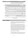
See drawing 32068A. This PCB contains a 12 bit A/D converter with built in
multiplexer (Linear Technology LTC1290), a 5 volt reference (Linear
Technology LTC1027), an inverter that supplies -13.5 volts for the analog
interface boards (LT1054), and a Dallas Semiconductor microcontroller
(DS87C520). Sample enable is inverted by Q1 to interrupt the microcontroller
and begin sampling. Analog channels 0 through 7 are converted in turn, a
conversion requiring approximately 20 microseconds. After all 8 conversions
have finished the system shift clock causes the microcontroller to shift the
binary data from the 8 conversions out onto pin 1. Most significant bit is
shifted out first.
The -13.5V supply is buffered through Q2 to ensure compatibility with a 9plus
that has a -15V supply in the top end cap.
Differential Amplifier / Low Pass Filter PCBs (AIF1 and AIF2)
See drawing 32156A. AIF1 and AIF2 are identical; AIF1 is for voltage channels
0 to 3 and AIF2 is for voltage channels 4 to 7. U1, U3, U4, and U6 are
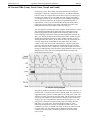
AD620BN differential amplifiers. The differential outputs are routed to four
low-pass filters, which are 2-pole Butterworth (maximally flat) types. They have
unity gain at dc and a gain of 0.707 at 5.5 Hz. The filters are of the singleamplifier follower type, which give extremely good gain accuracy because there
are no gain-setting resistors.
Components determining the filter frequency transfer characteristic have 1% or
2% tolerances and are stable with ambient temperature (i.e., metal film resistors
and Mylar capacitors respectively).
Modem PCB
Note:
The 300 baud modem interface, now
standard in the 9plus, was optional in
9plus CTDs with serial number 785
and lower.
See drawing 32023C. The Modem PCB mounts on stand-offs to the Sea Cable
Interface PCB on the top end cap, where it is sandwiched between the mounting
rails. +14.3 V power and the modem signals are obtained via interboard
connector J1. This is a 300 baud full-duplex circuit based on a Motorola
MC145443 modem chip (U5). A 6-pole active bandpass filter (U2 and U4 and
associated components) rejects the U3-buffered uplink FSK signal
(1070 - 1270 Hz), while passing the downlink signal (2025 - 2225 Hz). The
modem chip passes serial data to UART U7, which is controlled by a single-chip
microprocessor PXAG37KBA (U8). If the serial data uplink interface option is
installed, a logic to RS-232 level converter chip (U6, LT1081) provides access
to the modem channel from a terminal, computer, or serial-output instrument
connected to J2 via top end cap JT4. Control signals for the G.O. 1015 Rosette
Interface are available at J4, while the G.O. 1015 bottle trip confirm signal is
routed to the card file backplane from J3.
51