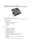
1
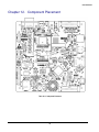
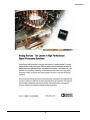
Renesas Demonstration Kit (RDK) for RX63N
User’s Manual: Hardware v3.2
R20UT2532EU0100
RENESAS MCU
RX Family / RX600 Series / RX63N Group
?
All information contained in these materials, including products and product specifications,
represents information on the product at the time of publication and is subject to change by
Renesas Electronics Corp. without notice. Please review the latest information published by
Renesas Electronics Corp. through various means, including the Renesas Electronics Corp.
website (http://www.renesas.com).
i
R20UT2532EU0100
Disclaimer
By using this Renesas Demonstration Kit (RDK), the user accepts the following terms. The RDK is not guaranteed to be error free, and the User
assumes the entire risk as to the results and performance of the RDK. The RDK is provided by Renesas on an “as is” basis without warranty of
any kind whether express or implied, including but not limited to the implied warranties of satisfactory quality, fitness for a particular purpose,
title and non-infringement of intellectual property rights with regard to the RDK. Renesas expressly disclaims all such warranties. Renesas or its
affiliates shall in no event be liable for any loss of profit, loss of data, loss of contract, loss of business, damage to reputation or goodwill, any
economic loss, any reprogramming or recall costs (whether the foregoing losses are direct or indirect) nor shall Renesas or its affiliates be liable
for any other direct or indirect special, incidental or consequential damages arising out of or in relation to the use of this RDK, even if Renesas
or its affiliates have been advised of the possibility of such damages.
Precautions
This Renesas Demonstration Kit is only intended for use in a laboratory environment under ambient temperature and humidity conditions. A
safe separation distance should be used between this and any sensitive equipment. Its use outside the laboratory, classroom, study area or
similar such area invalidates conformity with the protection requirements of the Electromagnetic Compatibility Directive and could lead to
prosecution.
The product generates, uses, and can radiate radio frequency energy and may cause harmful interference to radio communications. However,
there is no guarantee that interference will not occur in a particular installation. If this equipment causes harmful interference to radio or
television reception, which can be determined by turning the equipment off or on, you are encouraged to try to correct the interference by one or
more of the following measures:
•
Ensure attached cables do not lie across the equipment
•
Reorient the receiving antenna
•
Increase the distance between the equipment and the receiver
•
Connect the equipment into an outlet on a circuit different from that which the receiver is connected
•
Power down the equipment when not in use
•
Consult the dealer or an experienced radio/TV technician for help NOTE: It is recommended that wherever possible shielded interface
cables should be used.
The product is potentially susceptible to certain EMC phenomena. To mitigate against them it is recommended that the following measures be
undertaken:
•
The user is advised that mobile phones should not be used within 10m of the product when in use.
•
The user is advised to take ESD precautions when handling the equipment.
The Renesas Demonstration Kit does not represent an ideal reference design for an end product and does not fulfill the regulatory standards for
an end product.
ii
R20UT2532EU0100
Table of Contents
Chapter 1. Preface ................................................................................................................................................ 1
Chapter 2. Purpose ............................................................................................................................................... 2
Chapter 3. Power Supply ...................................................................................................................................... 4
3.1. Requirements ................................................................................................................................................. 4
3.2. Power – Up Behavior ..................................................................................................................................... 4
Chapter 4. Board Layout ....................................................................................................................................... 5
4.1. Board Layout .................................................................................................................................................. 5
4.2. Board Dimensions .......................................................................................................................................... 6
Chapter 5. Block Diagram ..................................................................................................................................... 7
Chapter 6. User Circuitry ...................................................................................................................................... 9
6.1. Pushbutton Switches ..................................................................................................................................... 9
6.2. Debug LCD Module ....................................................................................................................................... 9
6.3. LEDs ............................................................................................................................................................ 10
6.4. 3 – Axis Accelerometer ................................................................................................................................ 11
6.5. Digital Temp Sensor .................................................................................................................................... 11
6.6. Micron Serial Flash ...................................................................................................................................... 11
6.7. MicroSD Memory Card Slot ......................................................................................................................... 11
6.8. Potentiometer ............................................................................................................................................... 11
6.9. Serial port ..................................................................................................................................................... 11
6.10. Reset Circuit .............................................................................................................................................. 12
6.11. Audio (Audio Out, Mic, Speaker) ............................................................................................................... 12
6.12. RCAN ......................................................................................................................................................... 12
6.13. USB ............................................................................................................................................................ 13
6.14. Ethernet ..................................................................................................................................................... 14
6.15. Option Links and Jumper Settings ............................................................................................................. 15
6.16. Oscillator Sources ...................................................................................................................................... 18
iii
R20UT2532EU0100
6.17. Total Phase Beagle Debug Header ........................................................................................................... 18
Chapter 7. RX63N Operating Modes .................................................................................................................. 19
Chapter 8. Programming Methods ...................................................................................................................... 20
Chapter 9. Restoring the Factory Demo ............................................................................................................. 21
Chapter 10. Headers ........................................................................................................................................... 22
10.1. Extension Header 1 ................................................................................................................................... 22
10.2. Extension Header 2 ................................................................................................................................... 23
10.3. Application Header ..................................................................................................................................... 24
10.4. PMOD
TM
Interfaces .................................................................................................................................... 25
Chapter 11. Code Development ......................................................................................................................... 26
11.1. Overview .................................................................................................................................................... 26
11.2. Compiler Restrictions ................................................................................................................................. 26
11.3. Breakpoint Support .................................................................................................................................... 26
11.4. Memory Map .............................................................................................................................................. 27
Chapter 12. Component Placement ................................................................................................................... 28
Chapter 13. Additional Information ..................................................................................................................... 29
13.1. Hardware Partner Information ................................................................................................................... 29
Renesas Contact Information ............................................................................................................................. 42
iv
R20UT2532EU0100
R20UT2532EU0100
Chapter 1. Preface
Cautions
This document may be, wholly or partially, subject to change without notice.
All rights reserved. The RDK design, documentation, and demo software are intended to improve understanding and time-to-market for
RX63N-based designs. Duplication of the design, documentation, and demonstration software is encouraged.
Trademarks
All brand or product names used in this manual are trademarks or registered trademarks of their respective companies or organizations.
Copyright
© 2013 Renesas Electronics America, Inc. All rights reserved.
© 2013 Renesas Electronics Corporation. All rights reserved.
© 2013 Renesas Solutions Corporation. All rights reserved.
© 2013 Renesas Electronics Europe. All rights reserved.
Website:
http://www.renesas.com/
Glossary
ACCEL
Accelerometer
NC
No Connection
ADC
Analog-to-Digital Converter
PC
Program Counter
CAN
Controller Area Network
PCM
Phase-Change Memory
CPU
Central Processing Unit
POT
Potentiometer
DAC
Digital-to-Analog Converter
PMOD
Peripheral Module
EMC
Electromagnetic compatibility
RAM
Random Access Memory
ESD
Electrostatic Discharge
RCAN
Renesas Controller Area Network
HEW
High-performance Embedded
ROM
Read-Only Memory
RDK
Renesas Demonstration Kit
SDRAM
Synchronous Dynamic Random Access
Workshop
I/O
Input / Output
LCD
Liquid Crystal Display
LED
Light Emitting Diode
SD
Secured Digital
MCU
Microcontroller Unit
TEMP
Temperature
MIC
Microphone
VR
Variable Resistor
Memory
1
R20UT2532EU0100
Chapter 2. Purpose
This RDK is an evaluation and demonstration tool for Renesas RX63N microcontrollers. The goal is to provide the user with a powerful debug
and demonstration platform targeted at common applications. A set of human/machine interfaces are tightly integrated with the features of the
RX63N and the software demonstration programs providing the user with an accessible platform to rapidly evaluate and customize.
Target Applications and Features:
•
•
•
•
•
Audio
o
Stereo audio driver connected to the PWM interface
o
On-board microphone to demonstrate sampling, FFT/FPU capabilities
o
Volume Control Potentiometer
o
Micro SD card interface for audio and data files
Motor Control
o
3 – Phase motor control algorithm representation with LEDs
o
Motor control algorithm speed variation through volume control potentiometer
Gaming
o
3 – Axis Accelerometer (Digital)
o
User pushbutton switches
Communications
o
10/100 Ethernet Interface connected to an internal Ethernet MAC (1588 compatible)
o
USB Interface connected to an internal USB controller (Host, Device and OTG)
o
RS-232 Interface
o
CAN Interface
o
I2C, SPI with Debug through the Beagle connector from Total Phase
o
PMOD connections to support a variety of generic PMOD devices (WiFi, Bluetooth, RF, and much more).
User Code and Application Debugging
o
On-board J-Link OB for high-quality source code debugging
Develop and submit your sample programs to demonstrate these features to the online community: www.RenesasRulz.com
2
R20UT2532EU0100
The Renesas RDK user experience is complemented by the online Renesas ecosystem:
•
Renesas Interactive: www.RenesasInteractive.com
o
•
•
•
Free Online Learning
Renesas Rulz: www.RenesasRulz.com
o
Online community
o
Online user forums
o
www.RenesasRules.com/RX63N - Online support site for this RDK
University Program: www.RenesasUniversity.com
o
Support for Professors and Students
o
Support for University Kits (QSKs)
Renesas Microcontroller Samples (America Customers)
o
Free of charge
o
Request directly from www.America.Renesas.com/samples
3
R20UT2532EU0100
Chapter 3. Power Supply
3.1. Requirements
This RDK gets its power from the Segger J-Link OB USB connection or optionally from a regulated 5V power supply. The optional power jack is
a center positive connector using a 2.1 mm barrel.
Warning:
The RDK is neither under nor over-voltage protected.
Use a 5v REGULATED center positive supply which can source at
least 1 Amp.
3.2. Power – Up Behavior
The factory demo is based on two partner technologies:
-
Micrium’s RTOS kernel (uCOS-III), TCP-IP and HDCP networking stacks.
-
Exosite’s networked embedded systems and portal technology providing the cloud connectivity.
To boot up the factory demo:
-
Read the enclosed Exosite QSG
-
Install the factory DVD (version 1.0), included all provided drivers (JLINK).
-
Connect Ethernet cable to the RDK and your LAN connection
-
Connect the mini-USB cable to the JLink port, this will provide the debug link but also power (5 volts).
-
Watch the board boot-up sequence, displaying the board MAC address, IP address and cloud status.
-
The MAC address should match the address printed on the MAC Address sticker (right of the LCD display)
-
Register your board and address thru the Exosite portal website.
-
See your cloud status being updated to “connected”.
-
You are now ready to control your board through the Exosite portal.
4
R20UT2532EU0100
Chapter 4. Board Layout
4.1. Board Layout
The following diagram shows the top layer component layout.
5
R20UT2532EU0100
Figure 4-1: Board Layout
4.2. Board Dimensions
The following diagram gives the board dimensions and connector positions. All through hole connectors are on a common 0.1” grid for easy
interfacing.
Figure 4-2: Board Dimensions
6
R20UT2532EU0100
Chapter 5. Block Diagram
Figure 5-1 shows the CPU board components and their connectivity.
Figure 5-1: Block Diagram
7
R20UT2532EU0100
Figure 5-2 shows host PC connection to the RDK board and supporting partners.
USB
Figure 5-2: RDK Connections
8
R20UT2532EU0100
Chapter 6. User Circuitry
6.1. Pushbutton Switches
There are five pushbutton switches located on the CPU board. Table 6-1 shows the function of each pushbutton switch and its connection to the
MCU.
Switch
Function
MCU
SW1
Connects to an IRQ line for user controls.
P40, IRQ8-DS, Pin 95
SW2
Connects to an IRQ line for user controls.
P41, IRQ9-DS, Pin 93
SW3
Connects to an IRQ line for user controls.
P44, IRQ12-DS, Pin 90
SW4 (RESET)
When pressed, the RDK microcontroller and J-Link circuit are reset.
RES# , Pin 10
Table 6-1: Switch Functions
6.2. Debug LCD Module
A debug LCD module is supplied on the RDK. The debug LCD module uses an SPI interface to reduce the pin allocation. Software contrast
control is also provided. The module supplied with the RDK uses 3.3v. The display is a 96 x 64 graphics display and uses a white LED
backlight. The backlight is on by default and can be toggled OFF by setting MCU port P21 low. The backlight brightness can be also controlled
on a duty cycle using MTU pin MTIOC1B or TPU pin TIOCA3. Table 6-2 shows the pin allocation and signal names used for the graphics LCD
connector.
J11
Pin
Circuit Net Name
MCU
Pin
Circuit Net Name
MCU
1
+5V Backlight Positive Anode
-
2
BL_ENA
P21, pin 27
3
GND
-
4
GND
-
5
GND
-
6
LCD-CS
PC2, pin 50
7
RSTOUT# (Inverted RESET_IO)
PC3, pin 49 (inv)
8
LCD-RS
P51, pin 43
9
+3.3V
-
10
+3.3V
-
11
SCK
RSPCKA, pin 47
12
MOSI
MOSIA, pin 46
13
MOSI
MOSIA, pin 46
14
MOSI
MOSIA, pin 46
15
+3.3V
-
16
+3.3V
-
17
+3.3V
-
18
+3.3V
-
19
GND
-
20
+3.3V
-
Table 6-2: Debug LCD Module Connections
9
R20UT2532EU0100
6.3. LEDs
There are 17 LEDs on the RDK board.
•
The green ‘POWER’ LED (LED3) lights when the board is powered.
•
The Segger J-Link OB Debugger Interface LED (LED16) illuminates when the Debugger USB Interface is connected to a host PC.
•
There are 12 user LEDs (LED4-LED15) that are connected to IO ports. Each LED will light when their corresponding port pin is set
low. The 12 user LEDs are arranged to show the winding phases of a motor control circuit.
•
The remaining 2 LED’s (LED2 and LED1) are Ethernet specific, and are not accessed directly from the MCU.
Table 6-3 shows the user LED pin references and their corresponding microcontroller port pin connections.
LED Reference (As shown
Color
Circuit Net Name
MCU
LED1 (Speed ENET)
Green (On for 100BT)
-
N/A
LED2 (1PPS ENET)
Red
-
N/A
LED3 (5V Power)
Green
-
N/A
LED4
Green
LED6
PD5, pin 81
LED5
Green
LED12
PE3, pin 75
LED6
Red
LED3
PD2, pin 84
LED7
Red
LED9
PE0, pin 78
LED8
Green
LED5
PD4, pin 82
LED9
Green
LED11
PE2, pin 76
LED10
Red
LED2
PD1, pin 85
LED11
Red
LED8
PD7, pin 79
LED12
Green
LED4
PD3, pin 83
LED13
Green
LED10
PE1, pin 77
LED14
Red
LED1
PD0, pin 86
LED15
Red
LED7
PD6, pin 80
LED16 (Segger J-Link)
Green
-
N/A
D5 (USB Power)
Green
-
N/A
on silkscreen)
Table 6-3: LED Port
10
R20UT2532EU0100
6.4. 3 – Axis Accelerometer
The RDK includes an Analog Devices ADXL345 3–axis accelerometer. The part is connected to I2C SDA (MCU Pin 33) and SCL (MCU Pin 34).
I2C Address: 0x3A (0011101r) where r = R/W
6.5. Digital Temp Sensor
The RDK has component placement options for two Analog Devices digital temperature sensors (ADT7410TRZ or ADT75ARZ). Both are
connected to the I2C SDA (MCU Pin 33) and SCL pins (MCU Pin 34).
I2C Address = 0x90
ADT75 = (1001aaar) where aaa = A2:A1:A0, r=R/Wn
ADT7410 = (10010aar) where aa = A1:A0, r=R/Wn
6.6. Micron Serial Flash
A Micron Phase Change Memory (PCM) serial flash is provided for user non-volatile storage. PCM memory has greater write endurance than
standard serial flash. This part, NP5Q128A13ESFC0E, is 128 megabit and is accessed by the SPI Bus using SFL-CS (MCU Port PC0).
6.7. MicroSD Memory Card Slot
A MicroSD memory card slot is provided for file system data storage. This is configured to use SPI mode rather than nibble mode and is
accessed using SD-CS (MCU Port PC4).
6.8. Potentiometer
A single turn potentiometer is connected to the ADC channel AN002 of the microcontroller. This may be used to vary the analog voltage input
value to this pin between 3V3A and Ground. The potentiometer can also be used as a volume control through software.
Note: The potentiometer is fitted to offer an easy way of supplying a variable analog input to the controller. It does not necessarily reflect the
accuracy of the controllers ADC. Please see the device manual for details.
6.9. Serial port
The Serial module allows the MCU to communicate to a Host PC through the RS-232 connector, J5, using RS232Rx and RS232Tx. The serial
port is configured in DCE mode allowing direct connection to a PC without a Null modem. The serial module can also be used as a serial
debug port.
Table 6-4 contains details of the specific pin functions and their locations.
Description
Function
MCU Pin
Connector Pin
TXD2
Serial Transmission Pin
44
J5.2
RXD2
Serial Reception Pin
42
J5.3
Table 6-4: Serial port pin details
11
R20UT2532EU0100
6.10. Reset Circuit
The RDK includes a user reset switch (SW4) to reset both the RX63N MCU and Debugger MCU. This is connected to the internal reset circuit
on the RX63N (RES#) and input on the J-Link OB Segger Debugger.
There is a peripheral reset control line connected to PC2 (pin 49) on the RX63N which can be used to reset major peripherals at once. This
includes the Ethernet PHY, Beagle Port, Application Header, and Debug LCD.
6.11. Audio (Audio Out, Mic, Speaker)
An amplified stereo audio output jack is provided and connected to the timer circuit. Audio can be generated using a buffered output on TPU0 for
left (TIOCA0) and right (TIOCB0) channels. The headphone stereo amp is powered by a National Semi LM4808M. An on-board Analog
Devices Inc. (ADI) Silicon microphone (ADMP401) is connected to the ADC channel AN005 using an ADI SSM2167 low voltage Microphone
preamplifier. Note that the default is to have JP7, SPK EN, fitted. This enables the on-board Star Micronics speaker. Removing this jumper
disables the on-board speaker. Remove the jumper to use the headphone audio jack. The on-board speaker is powered by a SSM2377 audio
power amplifier to increase volume. Both the microphone and on-board speaker amplifiers can be turned OFF by setting AMP_SHDN (PA2)
low. DAC audio on the right channel is also supported using SPL SEL JP17.
Circuit Net Name
Function
MCU Pin
MCU Function
AUD_L
Audio Left
70
TIOCA0
AUD_R
Audio Right
29
TIOCB0
AN005
Microphone Analog In
89
AN005
AN002
Volume Control Analog In
92
AN002
AMP_SHDN
Mic. & On-board Speaker
68
PA2
Amp. Shutdown
AN006
Right Audio Analog Feedback
88
AN006
P05/DA1/IRQ13-A
DAC Right Audio Option (Can
100
DA1
select this option using JP17)
6.12. RCAN
The RCAN module can be controlled by the MCU through the CTx0 (Port pin P32) and CRx0 (Port pin P33) lines, or controlled externally
through the header connections CTx0 and CRx0.
The Table 6-5 contains details of the specific pin functions and their locations.
an 8 pin Renesas R2A25416SP CAN transceiver is fitted to the board.
Description
Function
MCU Pin
Header Pin
CTx0
RCAN Transmission Pin
18
CAN High J6.1
CRx0
RCAN Reception Pin
17
CAN Low J6.3
Table 6-5: RCAN port pin details
12
Note that
R20UT2532EU0100
6.13. USB
The USB module can be configured as Host, Function, or OTG with the correct switch settings on SW6.
•
Function / Device / Slave mode: This mode does not take any external power circuitry to implement. Simply put the SW6 DIP
switches to the proper setting as in table 6-7 and configure the software appropriately.
•
Host mode: Connect the included MiniAB to Host adapter Cable to have the proper cable connection for USB Host. This mode uses
U12 and associated passive circuitry to create USB Power. Set SW6 DIP switches to the settings shown in table 6-7. Note that you will
have to add an external 5V regulated supply that sources 1 Amp or greater to J4 in order to meet the USB Specification for power
delivery (500ma).
•
OTG: Set SW6 DIP switches to the settings shown in Table 6-7. Note that the Maxim MAX3353EEUE and associated circuitry will
create the proper USB OTG voltages. Note the Maxim IC must be configured in software using the I2C bus (Address 0x58) for proper
operation. Note that you will have to add an external 5V regulated supply that sources more than 1 Amp to J4 in order to meet the USB
Specification for power delivery (500ma).
Table 6-6 contains details of the USB signal descriptions and pin connections.
Description
Function
Microcontroller
Pin Number
USB_VBUS
USB cable connection monitor pin
30
USD+
USB data I/O pin
37
USD-
USB data I/O pin
36
VCC_USB
Power supply pin for USB built-in transceiver
35
VSS_USB
Ground pin for USB built-in transceiver
38
USB_DPUPE
Pull-up control pin
25
USB _ID
OTG USB ID
28
USB_OVRCURA
Host / OTG Over-current detect / Function Pull-up control pin B
32
USB_DRPD
D- Pull Down
26
USB_DPRPD
D+ Pull Down
23
USB0_EXICEN
Expansion
27
Table 6-6: USB Pin Definitions
Table 6-7 details how to set the SW6 DKP switches for each USB mode.
13
R20UT2532EU0100
USB DIP Switch Settings (SW6)
Mode No.
SW6.1
SW6.2
SW6.3
SW6.4
USB Host
OFF
OFF
ON
OFF
USB Function / device / slave
ON
OFF
OFF
ON
USB On the Go (OTG)
OFF
ON
OFF
ON
Table 6-7: USB DIP Switch SW6 settings
6.14. Ethernet
The Ethernet module conforms to the Ethernet or IEEE802.3 media access control (MAC) standard. The Ethernet controller is connected to the
direct memory access controller for Ethernet controller (E-DMAC) and carries out high-speed data transfer to and from the memory. In addition,
the Ethernet controller is connected to the National Semiconductor 10/100 Mbps DP83620SQE physical transceiver chip enabling it to perform
transmission and reception of Ethernet frames. Note that the chip is configured in Reduced Pin-count mode (RMII). The Ethernet PHY is
configured at power-on reset for Auto-Negotiation, advertising 10Base-T and 100Base-TX in both full and half-duplex modes.
Each RDK is pre-programmed in factory with a unique IEEE assigned MAC address ranging from 00:30:55:08:00:01 to 00:30:55:08:FF:FF. The
MAC address programmed into the part at the factory is shown on the front of the board and is stored in data flash at memory address 0x107FF0.
If there is a problem with the pre-programmed MAC address, the demonstration code will default to a default MAC address.
Table 6-8 contains details of the signal descriptions and pin connections. All connections to the MCU are direct.
Net Name
Function
MCU Pin
Number
ETH_CLK
Transmit/Receive Clock
58
TX_EN
Transmit Enable
56
RMII_TXD0
Transmit Data, Bit 1
55
RMII_TXD1
Transmit Data, Bit 2
54
RMII_MAS
Master Mode (high)
NC
RX_ER
Receive Error
57
RMII_RXD0
Receive Data, Bit 1
59
RMII_RXD1
Receive Data, Bit 2
61
CRS
Carrier Sense
53
MDC
Management Data Clock
66
MDIO
Management data I/O
67
ETH-IRQ
Power Down / Interrupt
98
Table 6-8: Ethernet Module Connections
14
R20UT2532EU0100
6.15. Option Links and Jumper Settings
Table 6-9 and Table 6-10 detail the function of the various option links contained on the RX63N RDK. There is also a 3-pin on-board speaker
function select jumper (JP17). By default, this jumper is set to play audio from the right audio channel (MCU pin 29) out the on-board speaker.
It can be cut and modified to use MCU pin 100 (P05/DA1) instead.
Table 6-9 details the Ethernet LED Configuration Resistor.
Ethernet Configuration Options
Reference
Function
Fitted
Alternative (Removed)
Related
To
R12
Ethernet
LED Configuration – Link/Activity (J1.L),
LED Configuration – Link (J1.L),
Configuration
Speed (LED14), Collision (J1.R)
Speed (LED14), Activity (J1.R)
Table 6-9: Ethernet Configuration Options
15
-
R20UT2532EU0100
Jumper Settings
Reference
JP7
Function
Open
Short
On Board Speaker Disabled
On Board Speaker Enabled
CAN terminator
Removes the CAN termination
CAN terminator active
disable
resistor – useful in some
Speaker
Notes
Enable
JP9
Cut the trace between the pads
to ‘open’ the circuit
debugging situations
JP10
JP11
JP12
JP13
Switch 3 acts on P42/AN2
Switch 3
Removes Switch 3 from
Isolation
P42/AN2 Circuit
Switch 3
Removes Switch 2 from
Isolation
P41/AN1 Circuit
Switch 3
Removes Switch 1 from
Isolation
P40/AN0 Circuit
J-Link Disable
J-Link OB debugger is active
J-Link OB is disabled with all
and works normally
output high impedance. This
Cut the trace between the pads
to ‘open the circuit
Switch 2 acts on P41/AN1
Cut the trace between the pads
to ‘open the circuit
Switch 1 acts on P40/AN0
Cut the trace between the pads
to ‘open the circuit
-
is useful for running a program
without the debugger or using
the boot mode of the RX63N
JP16
CAN Level
Disconnects CAN level shifter
Shifter Enable
from P33/CRx0_RXD6
CAN Level Shifter active
Cut the trace between the pads
to ‘open’ the circuit
Table 6-10 below describes the function of the jumper headers. The default configuration is indicated by BOLD text.
Jumper Settings
Reference
JP7
Function
Open
Short
On Board Speaker Disabled
On Board Speaker Enabled
CAN terminator
Removes the CAN termination
CAN terminator active
disable
resistor – useful in some
Speaker
Notes
Enable
JP9
Cut the trace between the pads
to ‘open’ the circuit
debugging situations
JP10
JP11
JP12
Switch 3
Removes Switch 3 from
Isolation
P42/AN2 Circuit
Switch 3
Removes Switch 2 from
Isolation
P41/AN1 Circuit
Switch 3
Removes Switch 1 from
Isolation
P40/AN0 Circuit
Switch 3 acts on P42/AN2
Cut the trace between the pads
to ‘open the circuit
Switch 2 acts on P41/AN1
Cut the trace between the pads
to ‘open the circuit
Switch 1 acts on P40/AN0
Cut the trace between the pads
to ‘open the circuit
16
R20UT2532EU0100
Jumper Settings
Reference
JP13
Function
Open
Short
J-Link Disable
J-Link OB debugger is active
J-Link OB is disabled with all
and works normally
output high impedance. This
Notes
-
is useful for running a program
without the debugger or using
the boot mode of the RX63N
JP16
CAN Level
Disconnects CAN level shifter
Shifter Enable
from P33/CRx0_RXD6
CAN Level Shifter active
Cut the trace between the pads
to ‘open’ the circuit
Table 6-10: Jumper header settings
17
R20UT2532EU0100
6.16. Oscillator Sources
All crystals are provided by NDK, Nihon Dempa Kogyo Co., LTD.
A crystal is fitted on the RDK and used to supply the main clock to the
Renesas microcontroller. Table 6-11 details the crystals that are fitted on the RX63N RDK.
Component
Part Number
Function
Frequency
Crystal (X1)
NX3225GA-12M
CPU/USB Clock
12 MHz
Crystal (X2)
NX3215SA-32K
CPU/RTC Clock
32.768 KHz
Crystal (X3)
NX3225GA-25M
Ethernet Clock
25 MHz
Crystal (X4)
NX3225GA-12M
J-Link OB System
12 MHz
Table 6-11: Oscillators / Resonators
6.17. Total Phase Beagle Debug Header
The Beagle I2C/SPI Protocol Analyzer is a non-intrusive USB-based bus monitor that can capture, display, and filter I2C and SPI data as it
appears on the bus. Using both the Data Center Software and Beagle analyzer, users can easily view I2C bus traffic (up to 4 MHz) and SPI bus
traffic (up to 24 MHz) in real time. Additional functionality allows engineers to filter data against a wide variety of parameters, or instantly search
for specific hexadecimal or ASCII data patterns during a live capture. The Beagle analyzer is fully supported on Windows, Linux, and Mac OS X,
and comes with free software, free APIs, free technical support, and free software/firmware upgrades.
Total Phase manufactures powerful and affordable USB, I2C, SPI, and CAN tools for embedded systems engineers. The complete line of Total
Phase host adapters and protocol analyzers are the development and debugging tools of choice for Fortune 500 companies, small businesses,
and research institutions all over the world.
For more technical information, online demos, and ordering information, visit www.totalphase.com.
18
R20UT2532EU0100
Chapter 7. RX63N Operating Modes
This RDK supports the 4 CPU modes: Debug Mode, Run Mode, USB Boot Mode and SCI Boot Mode.
and alter the state of MCU ports MD, PC7, and EMLE.
•
These modes are selected by SW5
The operating mode should only be set when the RDK is powered OFF.
Debugging mode is required for all debugging purposes. When the RDK is placed in Debug mode, a program will run unless a
debugging connection is made.
•
Run mode will disable MCU on-chip emulator communication and disable debugging.
•
USB and SCI boot modes allow debugging of the MCU through the user USB port (J9) and serial port (J5).
Table 7-1 details how to configure SW5 for each of these modes.
SW5.1
SW5.2
SW5.4
Debug Mode
OFF
OFF
ON
Run Mode
OFF
OFF
OFF
USB Boot Mode
ON
OFF
OFF
SCI Boot Mode
ON
ON
OFF
Table 7-1: MCU Operating Modes Table
19
R20UT2532EU0100
Chapter 8. Programming Methods
The RDK is intended for use with HEW, IAR, and KPIT Eclipse IDE software development tools. The board includes an on-board RX621 based
Segger J-Link OB debugger.
Refer to RX63N Group Hardware Manual for details of programming the microcontroller without using these
tools. The on-board J-Link OB is pre-programmed at the factory and configured for normal operation.
disabled by fitting a jumper to the J-Link disable 2-pin header (JP13).
mode.
The on-board debugger can be
This is useful if the board needs to be put into either USB or SCI boot
The RX621 based Segger J-Link OB is located under the Okaya LCD.
and can self-update later on if new versions are available.
20
The Jlink interface is pre-programmed at the factory final test
R20UT2532EU0100
Chapter 9. Restoring the Factory Demo
1.
To reload the Exosite/Micrium Factory Demo into the board, first set SW5 to Debug Mode (OFF, OFF, OFF, ON). Plug the USB cable to the J-link
connector of the RDK – the J-Link connector is above the display between the DB9 for the serial port and the power jack.
2.
Launch Renesas e2 studio: Start > All Programs > Renesas Electronics e2studio > Renesas e2studio.
3.
Unless you have installed the RDK’s DVD v3.2 that pre-loads the “Factory_Demo_Reload” project into the current workspace, you’ll need to import it
using this archive file : RDK_Demos.zip present in the DVD’s directory \Factory_demo (skip to Step 4 otherwise):
•
In the Top Menu bar, click File>Import click General and Existing Projects in Workspace, click Next
•
Select Archive File by clicking Browse to the DVD path, locate and select RDK_Demos.zip, click Open
•
Make sure to select the specific Project “Factory_Demo_Reload” and click Finish, the import will complete within minutes.
4.
In the Top Menu bar, click Run and select Debug Configurations
5.
Click Debug-only and click on Factory_Demo_Reload
6.
Click “Debug.” This step will re-program the RX63N Flash memory.
7.
If you are prompted to open the Debug perspective now, click “Yes.” This will open the main Debug window, and report that no source is available for
this project, this is normal.
8.
Restart the board by going to Run > Terminate, the RDK factory demo will reboot itself. You may close e2 studio now.
21
R20UT2532EU0100
Chapter 10. Headers
10.1. Extension Header 1
Table 10-1 shows the controller pin headers for JN1 and their corresponding microcontroller connections. The header pins connect directly to
the microcontroller pin.
JN1 Extension Header
Pin
Circuit Net Name
MCU Pin
Pin
Circuit Net Name
MCU Pin
1
5V0
-
2
Ground
-
3
3V3
-
4
Ground
-
5
3V3A
97
6
AGND
3, 94, 99
7
AVREF3V3
96
8
RESET#
10
9
SWITCH1 (P40/IRQ8-DS/AN000)
95
10
SWITCH2 (P41/IRQ9-DS/AN001)
93
11
SWITCH3 (P44/IRQ12-DS/AN004)
90
12
AN003 (P43/IRQ11-DS/AN003)
91
13
AN006 (P46/IRQ14-DS/AN006)
88
14
VREFH0_3V3
50
15
AGND
3, 94, 99
16
PMOD1_CS (PE4)
74
17
PMOD_SCK (PE5/RSPCKB)
73
18
PMOD_MOSI (PE6/MOSIB)
72
19
PMOD_MISO (PE7/MISOB)
71
20
MOSI (PC6/MOSI)
46
21
MISO (PC7/MISO)
45
22
SCK (PC5/SCK)
47
23
SFL-CS (PC0/SSLA1)
52
24
SD-CS (PC4/SSLA0)
48
25
SDA (P13/SDA)
33
26
SCL (P12/SCL)
34
Table 10-1: JN1 Extension Header
22
R20UT2532EU0100
10.2. Extension Header 2
Table 10-2 shows the controller pin headers for JN2 and their corresponding microcontroller connections. The header pins connect directly to
the microcontroller pin.
JN2 Extension Header
Pin
Circuit Net Name
1
RSTOUT#
3
MCU Pin
Pin
Circuit Net Name
MCU Pin
-
2
P53/BCLK
P35/NMI
15
4
Ground
5
PWMLP-OUT (Audio Generator)
40
6
PA6
64
7
PA7
63
8
P21 (BL_ENA)
27
9
PC1
51
10
NC
-
11
NC
-
12
NC
-
13
LED1 (PD0/IRQ0/AN008)
86
14
LED2 (PD0/IRQ0/AN008)
85
15
LED3 (PD2/IRQ2/AN010)
84
16
LED4 (PD3/IRQ3/AN011)
83
17
LED5 (PD4/IRQ4/AN012)
82
18
LED6 (PD5/IRQ5/AN013)
81
19
LED7 (PD6/IRQ6/AN6)
80
20
LED8 (PD7/IRQ7/AN7)
79
21
LED9 (PE0/ANEX0)
78
22
LED10 (PE1/ANEX1)
77
23
LED11 (PE2/AN0)
76
24
LED12 (PE3/AN1)
75
25
P24 (PMOD2_CS)
24
26
NC
Table 10-2: JN2 Extension Header
23
41
-
-
R20UT2532EU0100
10.3. Application Header
Table 10-3 shows the controller pin headers for J8 and their corresponding microcontroller connections. The header pins connect directly to
the microcontroller pin.
J8 Application Header
Pin
Circuit Net Name
MCU Pin
Pin
Circuit Net Name
MCU Pin
1
NC
-
2
GND
-
3
3V3
-
4
GND
-
5
NC
-
6
NC
-
7
NC
-
8
NC
-
9
NC
-
10
NC
-
11
NC
-
12
NC
-
13
NC
-
14
NC
-
15
SPI_CS (PJ3/WIFI-CS)
4
16
RSTOUT#
17
PWR_OFF (PE4)
74
18
NC
19
SPI_DIN (MOSI)
46
20
SPI_CLK (SCK)
47
21
UART_IN (CTx0_TXD6)
18*
22
SPI_DOUT (MISO)
45
23
SPI_INTR (WIFI-IRQ)
100
24
UART_OUT (CRx0_RXD6)
17
25
GPIO (PE5)
73*
26
GPIO (PE6)
72*
Table 10-3: J8 Application Header
24
10
-
R20UT2532EU0100
10.4. PMODTM Interfaces
Two Digilent PMODTM (Interface Type 2A, expanded SPI) connection headers are available on the RDK. These interfaces can be accessed on the
SPI bus using MCU port PE4 and P24 as chip selects. Table 10-4 shows the PMODTM headers and their corresponding microcontroller
connections.
PMOD1 (J15)
PMOD2 (J16)
Pin
Signal
Direction
Circuit Name
Function
Circuit Name
Function
1
Select
Out
PE4
PMOD1_CS
P24
PMOD2_CS
2
SDI
Out
PE6
PMOD_MOSI (MOSIB)
PE6
PMOD_MOSI (MOSIB)
3
SDO
In
PE7
PMOD_MISO (MISOB)
PE7
PMOD_MISO (MISOB)
4
SCK
Out
PE5
PMOD_SCK (RSPCKB)
PE5
PMOD_SCK (RSPCKB)
5
GND
-
GND
-
GND
-
6
VCC
-
3V3
-
3V3
-
7
IRQ
In
P55
PMOD_PIN7 (IRQ10)
P55
PMOD_PIN7 (IRQ10)
8
RST/IRQ
Out
PA1
PMOD_PIN8 (IRQ11)
PA1
PMOD_PIN8 (IRQ11)
9
GPIO
-
LED11
PMOD_PIN9 (PE2)
LED11
PMOD_PIN9 (PE2)
10
GPIO
-
LED10
PMOD_PIN10 (PE1)
LED10
PMOD_PIN10 (PE1)
11
GND
-
GND
-
GND
-
12
VCC
-
3V3
-
3V3
-
Table 10-4: PMOD Headers
25
R20UT2532EU0100
Chapter 11. Code Development
11.1. Overview
Note: For all code debugging using Renesas software tools, the CPU board must be connected to a PC USB port via the on-board Segger
J-Link OB debugger.
Due to the continuous process of improvements undertaken by Renesas the user is recommended to review the information provided on the
Renesas website at www.renesas.com/rdkRX63N to check for the latest updates to the Compiler and Debugger manuals.
11.2. Compiler Restrictions
We provided both the GNU, the IAR and Renesas Toolchains with this kit. The GNU RX Toolchain has NO restrictions. The RX compiler along
with HEW was used with ALL the Micrium uC/OS-III and Exosite example projects. The IAR size limitation, for the kickstart version, was
increased from 32KB to 64KB.
The Renesas Toolchain is fully functional for a period of 60 days from first use. After the first 60 days of use have expired, the compiler will
default to a maximum of 128k (code and data). To use the Renesas Toolchain with programs greater than this size you will need to purchase
the full version tools from your Renesas distributor. Renesas Tools Marketing team advises to start any new project with the e2 studio IDE.
Warning: The protection software for the compiler will detect changes to the system clock. Changing the system clock back in time
may cause the trial period to expire prematurely.
11.3. Breakpoint Support
Breakpoint support is directly supported by Segger J-Link OB emulator.
26
R20UT2532EU0100
11.4. Memory Map
H’0000 0000
On-Chip RAM
H’0001 8000
Reserved Area
H’0008 0000
Peripheral I/O Registers
H’0010 0000
On-chip ROM (data flash)
H’0010 8000
Reserved Area
H’007F 8000
FCU-RAM
H’007F A000
Reserved Area
H’007F C000
Peripheral I/O Registers
H’007F C500
Reserved Area
H’007F FC00
H’0080 0000
Peripheral I/O Registers
Reserved Area
H’00F8 0000
OnChip ROM (program ROM)
(Write Only)
H’0100 0000
On-Chip
Flash
H’FEFF E000
OnChip ROM (FCU firmware)
(Read Only)
H’FF00 0000
Reserved
H’FFF8 0000
OnChip ROM (program ROM)
(Read Only)
H’FFFF FFFF
Table 11-1: Memory Map
27
R20UT2532EU0100
Chapter 12. Component Placement
Table 121-1: Component Placement
28
R20UT2532EU0100
Chapter 13. Additional Information
13.1. Hardware Partner Information
Hardware partners played an integral role in the definition, development, and deployment of this RDK. Without their numerous contributions, this
project would not have been possible. Contributors include National Semiconductor for the DP83620 Precision PHYTER - IEEE1588 Precision
Time Protocol Ethernet transceiver and LP38500 3.3v regulator. Analog Devices supplied the ADXL345 3-Axis Accelerometer, SSM2167
microphone preamplifier and ADMP401 digital microphone, ADT7410TRZ (or ADT75ARZ) temp sensor, SSM2377 Audio Amplifier, and
ADM3101E RS-232 line driver / receiver. NDK contributed all 4 crystals for the board. Micron contributed their Phase Change Serial Flash
Memory (NP5Q128A13ESFC0E). Okaya provided the 96 x 64 backlit graphics LCD. Segger provided all the Debugger circuitry for their J-Link
OB. Star Micronics provided their NDT-03C speaker. TotalPhase provided the connectors to interface to their beagle serial channel debugger.
And finally, Future Designs, Inc. provided the hardware customization, schematic capture, PCB design and layout, manufacturing, and Supply
Chain Management services for this RDK. For more information or to contact our partners please refer to their websites:
•
Analog Devices – http://www.analog.com
•
Future Designs – http://www.teamfdi.com
•
Micron – http://www.micron.com
•
National Semiconductor – http://www.national.com
•
NDK - http://www.ndk.com
•
Okaya – http://www.okaya.com
•
Segger – http://www.segger.com
•
Seiko Instruments – http://www.seikoinstruments.com/
•
Totalphase – http://www.totalphase.com
29
R20UT2532EU0100
30
R20UT2532EU0100
31
R20UT2532EU0100
32
R20UT2532EU0100
33
R20UT2532EU0100
34
R20UT2532EU0100
35
R20UT2532EU0100
36
R20UT2532EU0100
37
R20UT2532EU0100
38
R20UT2532EU0100
39
R20UT2532EU0100
For educators and students.
The Alliance Partner Program allows
Gain the technical knowledge
Teach with professional
you to connect instantly with
you need. Evaluate, research, and learn at
grade tools. Learn MCUs
hundreds of qualified design consulting
your own pace, where and when you want, for
with a modern architecture.
and contracting professionals.
free.
RenesasUniversity.com
renesas.com/Alliance
RenesasInteractive.com
Renesas Samples
Customize your data
Get a first-hand look at our products.
A forum and community site
retrieval needs on the Renesas
Let us know your needs,
and we'll get some samples out to
you. It's that simple.
to share technical information,
web site. You'll receive
updates on the product that
RenesasSamples.com
questions and opinions with
others who use Renesas MCUs
you're interested in.
and MPUs.
renesas.com/MyRenesas
RenesasRulz.com
Software Library
Access a wealth of information to
speed you along on your designs.
40
R20UT2532EU0100
renesas.com/software
41
R20UT2532EU0100
Renesas Contact Information
For details on how to use High-performance Embedded Workshop (HEW), refer to the HEW manual available on the web site.
For information about the RX63N series microcontrollers refer to the RX600 Group hardware manual.
For information about the RX63N assembly language, refer to the RX Series Software Manual.
For more information about e2 Studio software, please visit : http://www.renesas.com/products/tools/ide/ide_e2studio/index.jsp
Online technical support and information is available at: http://www.RenesasRulz.com
Technical Contact Details
America:
[email protected]
Europe:
[email protected]
Japan:
[email protected]
General information on Renesas Microcontrollers can be found on the Renesas website at: http://www.renesas.com/
42
Renesas Demonstration Kit (RDK) for RX63N
User's Manual
R20UT2532EU0100
Publication Date
Rev.3.2
Published by:
Renesas Electronics America, Inc.
30 July 2013
2880 Scott Boulevard
Santa Clara, CA 95050-2554, U.S.A
©2013 Renesas Electronics America, All Rights Reserved.
RX63N Group
Renesas Electronics America, Inc.
2880 Scott Boulevard
Santa Clara, CA 95050-2554, U.S.A