1
GR712RC
Dual-Core LEON3FT SPARC V8 Processor
2015 User’s Manual
The most important thing we build is trust
GR712RC
Dual-Core LEON3FT SPARC V8 Processor
User’s Manual
GR712RC-UM, Nov 2015, Version 2.6
www.combham.com/gaisler
GR712RC
Table of contents
1
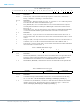
Introduction........................................................................................................... 7
1.1
1.2
1.3
1.4
1.5
1.6
1.7
1.8
Scope...................................................................................................................... 7
GR712RC Architecture .......................................................................................... 7
Memory map .......................................................................................................... 8
Interrupts ................................................................................................................ 9
GRLIB IP cores...................................................................................................... 9
References............................................................................................................ 10
Errata.....................................................................................................................11
Document revision history ................................................................................... 18
2
Signals and I/O Switch Matrix........................................................................... 21
3
Clocking ............................................................................................................... 31
3.1
3.2
3.3
3.4
3.5
3.6
3.7
3.8
3.9
3.10
4
LEON3FT - High-performance SPARC V8 32-bit Processor......................... 35
4.1
4.2
4.3
4.4
4.5
4.6
4.7
4.8
4.9
5
System clock ........................................................................................................ 31
SpaceWire clock................................................................................................... 31
MIL-STD-1553 .................................................................................................... 32
Telemetry ............................................................................................................. 32
Telecommand ....................................................................................................... 32
Obsolete ............................................................................................................... 32
SLINK.................................................................................................................. 32
SDRAM clock...................................................................................................... 33
Clock gating unit.................................................................................................. 33
Test mode clocking .............................................................................................. 34
Overview.............................................................................................................. 35
LEON3 integer unit.............................................................................................. 36
Instruction cache .................................................................................................. 43
Data cache ............................................................................................................ 44
Additional cache functionality ............................................................................. 44
Memory management unit ................................................................................... 47
Floating-point unit................................................................................................ 49
Error detection and correction.............................................................................. 49
Signal definitions ................................................................................................. 51
Fault Tolerant Memory Controller.................................................................... 52
5.1
5.2
5.3
5.4
5.5
5.6
5.7
5.8
5.9
5.10
5.11
Overview.............................................................................................................. 52
PROM access ....................................................................................................... 53
Memory mapped IO ............................................................................................. 55
SRAM access ....................................................................................................... 56
8-bit PROM and SRAM access ........................................................................... 57
8- bit I/O access.................................................................................................... 58
Burst cycles .......................................................................................................... 58
SDRAM access .................................................................................................... 58
Refresh ................................................................................................................. 59
Memory EDAC .................................................................................................... 61
Bus Ready signalling ........................................................................................... 63
GR712RC-UM, Nov 2015, Version 2.6
2
www.combham.com/gaisler
GR712RC
5.12
5.13
5.14
5.15
6
On-chip Memory with EDAC Protection ......................................................... 69
6.1
6.2
6.3
7
Overview.............................................................................................................. 89
Operation.............................................................................................................. 89
Registers............................................................................................................... 90
General Purpose Register................................................................................... 92
13.1
13.2
14
Overview.............................................................................................................. 86
Operation.............................................................................................................. 86
Registers............................................................................................................... 87
Signal definitions ................................................................................................. 88
General Purpose Timer Unit with Time Latch Capability.............................. 89
12.1
12.2
12.3
13
Overview.............................................................................................................. 84
Operation.............................................................................................................. 84
Registers............................................................................................................... 85
Signal definitions ................................................................................................. 85
General Purpose Timer Unit.............................................................................. 86
11.1
11.2
11.3
11.4
12
Overview.............................................................................................................. 77
Operation.............................................................................................................. 77
AHB Trace Buffer ................................................................................................ 78
Instruction trace buffer......................................................................................... 79
DSU memory map ............................................................................................... 80
DSU registers ....................................................................................................... 81
JTAG Debug Interface........................................................................................ 84
10.1
10.2
10.3
10.4
11
Overview.............................................................................................................. 72
Operation.............................................................................................................. 72
Registers............................................................................................................... 74
Hardware Debug Support Unit ......................................................................... 77
9.1
9.2
9.3
9.4
9.5
9.6
10
Overview.............................................................................................................. 71
Operation.............................................................................................................. 71
Registers............................................................................................................... 71
Multiprocessor Interrupt Controller................................................................. 72
8.1
8.2
8.3
9
Overview.............................................................................................................. 69
Operation.............................................................................................................. 69
Registers............................................................................................................... 70
AHB Status Registers ......................................................................................... 71
7.1
7.2
7.3
8
External bus errors ............................................................................................... 64
Read strobe........................................................................................................... 65
Registers............................................................................................................... 65
Signal definitions ................................................................................................. 68
Operation.............................................................................................................. 92
Registers............................................................................................................... 92
General Purpose I/O Port .................................................................................. 93
14.1
14.2
14.3
Overview.............................................................................................................. 93
Operation.............................................................................................................. 93
Registers............................................................................................................... 95
GR712RC-UM, Nov 2015, Version 2.6
3
www.combham.com/gaisler
GR712RC
14.4
15
UART Serial Interface ........................................................................................ 97
15.1
15.2
15.3
15.4
15.5
15.6
15.7
15.8
16
Overview............................................................................................................ 135
CAN controller overview................................................................................... 135
AHB interface .................................................................................................... 135
BasicCAN mode ................................................................................................ 136
PeliCAN mode ................................................................................................... 140
Common registers .............................................................................................. 150
Design considerations ........................................................................................ 151
Signal definitions ............................................................................................... 151
Obsolete.............................................................................................................. 152
19.1
20
Overview............................................................................................................ 127
Operation............................................................................................................ 127
Tx DMA interface .............................................................................................. 128
Rx DMA interface.............................................................................................. 129
MDIO Interface.................................................................................................. 131
Reduced Media Independent Interfaces (RMII) ................................................ 131
Registers............................................................................................................. 131
Signal definitions ............................................................................................... 134
CAN Interface ................................................................................................... 135
18.1
18.2
18.3
18.4
18.5
18.6
18.7
18.8
19
Overview............................................................................................................ 102
Operation............................................................................................................ 102
Link interface ..................................................................................................... 103
Receiver DMA channels .................................................................................... 105
Transmitter DMA channels .................................................................................111
RMAP .................................................................................................................114
AMBA interface..................................................................................................119
SpaceWire clock generation............................................................................... 120
Registers............................................................................................................. 121
Signal definitions ............................................................................................... 126
Ethernet Media Access Controller (MAC) ..................................................... 127
17.1
17.2
17.3
17.4
17.5
17.6
17.7
17.8
18
Overview.............................................................................................................. 97
Operation.............................................................................................................. 97
Baud-rate generation ............................................................................................ 98
Loop back mode................................................................................................... 98
FIFO debug mode ................................................................................................ 99
Interrupt generation.............................................................................................. 99
Registers............................................................................................................... 99
Signal definitions ............................................................................................... 101
SpaceWire Interface with RMAP support...................................................... 102
16.1
16.2
16.3
16.4
16.5
16.6
16.7
16.8
16.9
16.10
17
Signal definitions ................................................................................................. 96
Signal definitions ............................................................................................... 152
CAN Bus multiplexor........................................................................................ 153
20.1
20.2
20.3
Overview............................................................................................................ 153
Operation............................................................................................................ 153
Registers............................................................................................................. 153
GR712RC-UM, Nov 2015, Version 2.6
4
www.combham.com/gaisler
GR712RC
21
MIL-STD-1553B BC/RT/BM .......................................................................... 154
21.1
21.2
21.3
21.4
21.5
22
I2C-master ......................................................................................................... 159
22.1
22.2
22.3
22.4
23
Overview............................................................................................................ 179
Operation............................................................................................................ 179
Registers............................................................................................................. 180
Signal definitions ............................................................................................... 182
GRTC - Telecommand Decoder....................................................................... 183
26.1
26.2
26.3
26.4
26.5
26.6
26.7
26.8
26.9
26.10
27
Overview............................................................................................................ 171
Operation............................................................................................................ 171
Registers............................................................................................................. 174
Signal definitions ............................................................................................... 178
ASCS Controller................................................................................................ 179
25.1
25.2
25.3
25.4
26
Overview............................................................................................................ 165
Operation............................................................................................................ 165
Registers............................................................................................................. 167
Signal definitions ............................................................................................... 170
SLINK Serial Bus Based Real-Time Network Master................................... 171
24.1
24.2
24.3
24.4
25
Overview............................................................................................................ 159
Operation............................................................................................................ 159
Registers............................................................................................................. 162
Signal definitions ............................................................................................... 164
SPI Controller.................................................................................................... 165
23.1
23.2
23.3
23.4
24
Overview............................................................................................................ 154
AHB interface .................................................................................................... 155
1553 Clock generation ....................................................................................... 155
Registers............................................................................................................. 157
Signal definitions ............................................................................................... 158
Overview............................................................................................................ 183
Data formats....................................................................................................... 184
Coding Layer (CL)............................................................................................. 185
Transmission ...................................................................................................... 187
Relationship between buffers and FIFOs........................................................... 190
Command Link Control Word interface (CLCW) ............................................. 192
Configuration Interface (AMBA AHB slave) .................................................... 192
Miscellaneous..................................................................................................... 193
Registers............................................................................................................. 194
Signal definitions ............................................................................................... 201
GRTM - CCSDS Telemetry Encoder .............................................................. 202
27.1
27.2
27.3
27.4
27.5
27.6
27.7
Overview............................................................................................................ 202
References.......................................................................................................... 203
Layers................................................................................................................. 204
Data Link Protocol Sub-Layer ........................................................................... 205
Synchronization and Channel Coding Sub-Layer.............................................. 207
Physical Layer.................................................................................................... 210
Connectivity ....................................................................................................... 212
GR712RC-UM, Nov 2015, Version 2.6
5
www.combham.com/gaisler
GR712RC
27.8
27.9
27.10
28
Clock Gating Unit ............................................................................................. 221
28.1
28.2
28.3
29
Operation............................................................................................................ 213
Registers............................................................................................................. 216
Signal definitions ............................................................................................... 220
Overview............................................................................................................ 221
Operation............................................................................................................ 221
Registers............................................................................................................. 222
LEON3 Configuration ...................................................................................... 223
29.1
29.2
29.3
29.4
29.5
29.6
CPU.................................................................................................................... 223
Cache configuration ........................................................................................... 223
Memory Management Unit (MMU) .................................................................. 223
Floating Point Unit (FPU).................................................................................. 224
Debug Support Unit (DSU)................................................................................ 224
Fault tolerance.................................................................................................... 224
GR712RC-UM, Nov 2015, Version 2.6
6
www.combham.com/gaisler
GR712RC
1
Introduction
1.1
Scope
This document is a user’s manual for the radiation-hard GR712RC Dual-Core LEON3FT SPARC V8
processor. GR712RC is based on LEON3FT and IP cores from the GRLIB IP library, implemented
with the Ramon RadSafeTM 180 nm cell library on Tower Semiconductors 180nm CMOS process.
1.2
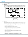
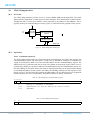
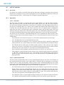
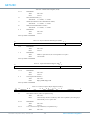
GR712RC Architecture
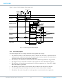
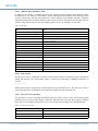
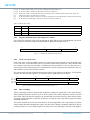
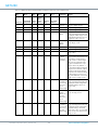
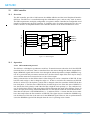
The GR712RC has the following on-chip features:
• 2 x LEON3FT processor cores with 32KiB cache and 32-entry TLB SRMMU
• 2 x Double-precision high-performance floating-point units (GRFPU V2)
• Debug Support Unit (DSU) with 256-line instruction and AMBA AHB trace buffers
• PROM/SRAM/SDRAM memory controller with BCH and Reed-Solomon error-correction
• up to 32 MiB PROM over two 16 MiB banks
• up to 32 MiB SRAM over two 16 MiB banks
• up to 1 GiB SDRAM over two 512 MiB banks
• 192 KiB on-chip RAM with BCH error-correction (uncacheable)
• 6 x SpaceWire links (two with RMAP support, one DMA channel per link, one port per link)
• 6 x UARTs
• 6 x General Purpose Timers (2 with time latch capability)
• Multi-processor Interrupt Controller with support for 31 interrupts
• 2 x 32 bits General Purpose I/O
• JTAG debug link
• 10/100 Ethernet MAC with RMII interface
• MIL-STD-1553B BC/RT/BM controller
• 2 x CAN 2.0 controller
• High-speed CCSDS Telecommand decoder and Telemetry encoder
• SPI master controller
• I2C master controller
• SLINK and ASCS16 controllers
• Clock gating unit
• I/O switch matrix
JTAG
LEON3FT
AHB
Control
LEON3FT
Debug
Support Unit
JTAG
Debug Link
1553
CAN
TMTC
1553
BC/RT/BM
2xCAN
TM &
TC
SpaceWire
6xSpW
RAM
192K
AMBA AHB
Memory
Controller
AHB/APB
Bridge
AMBA APB
6xUART
Timers
RS232
WDOGN
IrqCtrl
I/O port
ASCS
Ethernet
MAC
SPI
I2C
SPI
I2C ASCS16 SLINK ETH PHY
SLINK
8/32-bits memory bus
PROM
I/O
SRAM
SDRAM
GPIO
GR712RC Block diagram
GR712RC-UM, Nov 2015, Version 2.6
7
www.combham.com/gaisler
GR712RC
1.3
Memory map
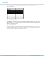
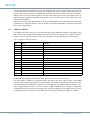
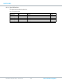
The memory map of the internal AHB/APB buses is specified as shown below.
TABLE 1. Internal memory map
Core
Address range
FTMCTRL
0x00000000 - 0x20000000
0x20000000 - 0x40000000
0x40000000 - 0x80000000
Bus
PROM area
I/O area
SRAM/SDRAM area
AHB
AHB
APBCTRL - 1
0x80000000 - 0x80100000
APB bridge
FTMCTRL
0x80000000 - 0x80000100
Registers
APB
APBUART - 0
0x80000100 - 0x80000200
Registers
APB
IRQMP
0x80000200 - 0x80000300
Registers
APB
GPTIMER
0x80000300 - 0x80000400
Registers
APB
SPICTRL
0x80000400 - 0x80000500
Registers
APB
CANMUX
0x80000500 - 0x80000600
Registers
APB
GRGPREG
0x80000600 - 0x80000700
Registers
APB
GRASCS
0x80000700 - 0x80000800
Registers
APB
GRSLINK
0x80000800 - 0x80000900
Registers
APB
GRGPIO - 1
0x80000900 - 0x80000A00
Registers
APB
GRGPIO - 2
0x80000A00 - 0x80000B00
Registers
APB
GRTM
0x80000B00 - 0x80000C00
Registers
APB
I2CMST
0x80000C00 - 0x80000D00
Registers
APB
CLKGATE
0x80000D00 - 0x80000E00
Registers
APB
GRETH
0x80000E00 - 0x80000F00
Registers
APB
APB
AHBSTAT
0x80000F00 - 0x80001000
Registers
APB1 plug&play
0x800FF000 - 0x80100000
Plug&play configuration
APB
APBCTRL - 2
0x80100000 - 0x80200000
APB bridge
AHB
APBUART - 1
0x80100100 - 0x80100200
Registers
APB
APBUART - 2
0x80100200 - 0x80100300
Registers
APB
APBUART - 3
0x80100300 - 0x80100400
Registers
APB
APBUART - 4
0x80100400 - 0x80100500
Registers
APB
APBUART - 5
0x80100500 - 0x80100600
Registers
APB
GRTIMER
0x80100600 - 0x80100700
Registers
APB
GRSPW2 - 0
0x80100800 - 0x80100900
Registers
APB
GRSPW2 - 1
0x80100900 - 0x80100A00
Registers
APB
GRSPW2 - 2
0x80100A00 - 0x80100B00
Registers
APB
GRSPW2 - 3
0x80100B00 - 0x80100C00
Registers
APB
GRSPW2 - 4
0x80100C00 - 0x80100D00
Registers
APB
GRSPW2 - 5
0x80100D00 - 0x80100E00
Registers
APB
APB2 plug&play
0x801FF000 - 0x80200000
Plug&play configuration
APB
DSU3
0x90000000 - 0xA0000000
Registers
AHB
FTAHBRAM
0xA0000000 - 0xA0100000
0x80100000 - 0x80100100
RAM area
Registers
AHB
APB
B1553BRM
0xFFF00000 - 0xFFF01000
Registers
AHB
GRTC
0xFFF10000 - 0xFFF10100
Registers
AHB
Proprietary, do not access
0xFFF20000 - 0xFFF20100
Registers
AHB
CANOC
0xFFF30000 - 0xFFF31000
Registers
AHB
AHB plug&play
0xFFFFF000 - 0xFFFFFFFF
Plug&play configuration
AHB
Access to addresses outside the ranges described above returns an AMBA AHB error response.
GR712RC-UM, Nov 2015, Version 2.6
8
www.combham.com/gaisler
GR712RC
1.4
Interrupts
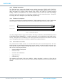
The following table specifies the interrupt assignment for the GR712RC.
TABLE 2. Interrupt assignment
Core
Interrupt #
Function
AHBSTAT
1
AHB bus error
APBUART - 0
2
UART1 RX/TX interrupt
GRGPIO - 1 to 2
1-15
External I/O interrupt (3 & 4 are GPIO only)
CANOC
5-6
OCCAN interrupt (core 1 - 2)
GRTIMER
7
GRTIMER timer underflow interrupt
GPTIMER
8-11
GPTIMER timer underflow interrupts
IRQMP
12
IRQMP extended interrupt
SPICTRL, SLINK
13
SPI and SLINK interrupt
B1553BRM, GRETH, GRTC
14
1553, Ethernet, and Telecommand interrupt
ASCS
16
ASCS interrupt
APBUART - 1to 5
17-21
UART2-6 RX/TX interrupt
GRSPW2 - 0 to 5
22-27
SpaceWire 0-5 RX/TX data interrupt
I2CMST
28
I2C master interrupt
GRTM
29
Telemetry encoder interrupt
30
Telemetry encoder time strobe interrupt
The interrupts are routed to the IRQMP interrupt controller and forwarded to the LEON3FT processors. Interrupt 16-31 are generated as interrupt 12 and for those interrupts a chained interrupt handler
is used.
1.5
GRLIB IP cores
The GR712RC uses the following cores from the GRLIB IP library:
TABLE 3. Used IP cores
Core
Function
Vendor ID
Device ID
LEON3FT
Fault tolerant SPARC V8 32-bit processor
0x01
DSU3
Debug support unit
0x01
0x053
0x004
IRQMP
Interrupt controller
0x01
0x00D
APBCTRL
AHB/APB Bridge
0x01
0x006
FTMCTRL
8/32-bit Memory controller with EDAC
0x01
0x054
AHBSTAT
AHB failing address register
0x01
0x052
FTAHBRAM
Fault tolerant on chip memory
0x01
0x050
AHBJTAG
JTAG/AHB debug interface
0x01
0x01C
GRSPW2
SpaceWire link with DMA
0x01
0x029
B1553BRM
MIL-STD1553B BC/RT/BM controller
0x01
0x072
CANOC
OC CAN controller
0x01
0x019
GRETH
10/100 Ethernet MAC
0x01
0x01D
0x00C
APBUART
8-bit UART with FIFO
0x01
GPTIMER
Modular timer unit
0x01
0x011
GRTIMER
Modular timer unit with time latch capability
0x01
0x038
GRGPIO
General purpose I/O port
0x01
0x01A
GRTC
CCSDS Telecommand Decoder
0x01
0x031
GRTM
CCSDS Telemetry Encoder
0x01
0x030
-
Proprietary
0x01
0x080
CANMUX
CAN bus multiplexer
0x01
0x081
GR712RC-UM, Nov 2015, Version 2.6
9
www.combham.com/gaisler
GR712RC
TABLE 3. Used IP cores
Core
1.6
Function
Vendor ID
Device ID
GRASCS
ASCS16 controller
0x01
0x043
GRSLINK
SLINK controller
0x01
0x02F
SPICTRL
SPI controller (master only)
0x01
0x02D
I2CMST
I2C master
0x01
0x028
CLKGATE
Clock gating unit
0x01
0x02C
GRGPREG
General purpose register
0x01
0x087
References
[DS]
[SPARC]
GR712RC - Dual-Core LEON3FT SPARC V8 Processor, Data Sheet, GR712RC-DS,
Issue 2.1, June 2014, Cobham Gaisler, www.cobham.com/gaisler
The SPARC Architecture Manual, Version 8, Revision SAV080SI9308, SPARC
International Inc.
[SPW]
ECSS - Space Engineering, SpaceWire - Links, Nodes, Routers and Networks,
ECSS-E-ST-50-12C, 31 July 2008
[RMAPID]
ECSS - Space Engineering, SpaceWire Protocol Identification, ECSS-E-ST-50-51C,
February 2010
[RMAP]
ECSS - Space Engineering, Remote Memory Access Protocol, ECSS-E-ST-50-52C,
February 2010
[1553BRM]
Core1553BRM Product Handbook, 50200040-0/11-04, November 2004, Actel Corporation
Core1553BRM MIL-STD-1553 BC, RT, and MT, 51700052-4/12.05, v 5.0,
December 2005, Actel Corporation
Core1553BRM User's Guide, 50200023-0/06.04, June 2004, Actel Corporation
[MMU]
[GRETH]
Core1553BRM v2.16 Release Notes, 51300019-8/6.06, June 2006, Actel Corporation
Technical Note on LEON SRMMU Behaviour, GRLIB-TN-0002, Issue 1,
Revision 1, February 2015, Cobham Gaisler, www.comham.com/gaisler
Technical Note on GRETH Controller Behaviour, GRLIB-TN-0008, Issue 1,
October 2015, Cobham Gaisler, www.cobham.com/gaisler
GR712RC-UM, Nov 2015, Version 2.6
10
www.combham.com/gaisler
GR712RC
1.7
Errata
1.7.1 FTAHBRAM: On-chip Memory not cacheable
The 192 KiB on-chip memory at address 0xA00000000 is not cacheable in the L1 caches of the processors. This means that executing from the on-chip memory will be slow, approximately 0.25 MIPS/
MHz. The on-chip memory should preferably be used for data storage for on-chip IP cores, such as
the Mil-Std-1553B controller, Ethernet controller and SpaceWire links.
See sections 4.2.15 and 6.1 for details.
1.7.2 CAN OC: interrupt can be cleared before read
The Transmit Interrupt can be cleared before read, if a read access is made to the Interrupt Register in
the same clock cycle as the interrupt is set by the transmitter logic.
Instead of looking at the Transmit Interrupt flag, the Transmit Buffer Status flag in the Status Register
can bee looked at when something has been scheduled for transmission.
See section 18.4.5.
1.7.3 GRSPW2: interrupt can be lost
If an AMBA AHB error occurs in the same clock cycle as a SpaceWire link error or Time-Code TickOut interrupt is generated and the AMBA AHB error interrupts are disabled then the corresponding
interrupt will be lost (i.e. SpaceWire link error or Time-Code Tick-Out interrupt)
The workaround is to always have AMBA AHB error interrupt enabled (AHB Error Interrupt (AI) in
GRSPW DMA Control Register) if the other two interrupts are used (Interrupt Enable (IE) in
GRSPW Control Register). An AMBA AHB error interrupt will cause the GRSPW2 core to stop, and
therefore interrupt handling will be required anyway.
See section 16.9.
1.7.4 GRSPW2: CRC calculation partially incorrect
RMAP CRC calculation for the DMA receiver does not work correctly under all conditions. The
detected header length is not used correctly in cases when two characters are received on consecutive
cycles and one of them is the header CRC. This results in an incorrect header CRC indication in the
receiver descriptor (i.e. Header CRC (HC) field). The calculation is continued however (as described
in the manual) and the data CRC indication (i.e. Data CRC (DC) field) is still correct and covers the
whole packet and can thus be used to determine that there are no errors in the complete packet.
See section 16.4.5.
1.7.5 SPICTRL: transfers in progress bit not cleared
The Transfer in Progress bit (TIP the core's Event Register is not cleared automatically by the core if
an overrun occurs. The core needs to be disabled in order to clear the bit. The problem does not affect
most software drivers.
Workaround 1: Read receive queue so that no overrun occurs.
Workaround 2: Disable and re-enable core if overrun occurs.
Workaround 3: Do not use Transfer in Progress (TIP) interrupts.
See section 23.3.
1.7.6 SPICTRL: back-to-back transfers
Back-to-back transfers where a word is written to the core's transmit queue at the very end of the
transfer of a previous word may cause the core to essentially change the clock phase (CPHA) of the
SPI communication. This leads to transmission and reception of wrong data.
The SPI controller regards a transfer as completed when the last bit has been sampled. With clock
phase 1 there is a window between sampling of the last bit and when the SCK clock line returns to its
idle state. If a new transfer is started (a word is written to the core's transmit queue) in this window,
then the bug will be triggered.
GR712RC-UM, Nov 2015, Version 2.6
11
www.combham.com/gaisler
GR712RC
This scenario can occur when writing a series of words to the SPI controller and the delay between
two writes matches the time it takes for the core to transfer the current transmit queue contents. A possible scenario is that a processor wants to send two words over SPI, after the first word has been written the processor gets an interrupt, when the processor returns from serving the interrupt and writes
the second word the second write could hit the window.
Software drivers that use SPI clock phase 0 (data sampling starts on the first transition of SCK) are
potentially affected.
Workaround 0: Use a SPI clock phase of 1 and adjust the CPOL value instead.
Workaround 1: Ensure that all words of a transfer are written to the transmit queue before the last bit
of a preceding word has been sent.
See section 23.3.
1.7.7 FTMCTLR: EDAC usage with 8-bit wide memory
The FTMCTRL - 8/16/32-bit Memory Controller with EDAC IP core supports EDAC protection of
8-bit wide PROM and SRAM banks. The implementation has a shortcoming that prevents a contiguous data area stretching over multiple banks to be protected with EDAC when using memory devices
with 8-bit wide data buses. It has therefore been documented in user's manuals that only the first
PROM bank and the first SRAM bank can be used with EDAC protection of 8-bit wide data.
Detailed analysis shows however that the limitation of using only one bank applies to the usage of a
contiguous memory space. It is in fact possible to use multiple banks (i.e. multiple chip select signals)
in 8-bit wide operation with EDAC protection, provided that the memory space can be not contiguous. The checkbytes for the device in each bank are stored at the top addresses of the actual device.
Thus 80% of each device can be utilized but there will consequently be gaps in the user data.
For this scheme to work with GR712RC it is mandatory that the bank size is defined as at least 4
times larger than the actual memory device mapped to the bank. Thus the gaps in the user data will be
larger than the expected 20% imposed by the checkbytes, since now the distance between the start of
each bank is at least four times the memory device size. The governing principle is that the actual
memory device size must not be larger than a quarter of the bank size for this scheme to work for
more than 2 PROM banks. Note that more than 2 PROM banks can be decoded in the GR712RC,
although only 2 external chip select signals are provided.
For this scheme to work with 2 PROM banks (due to programming) there is no limitation on the size
of the actual memory device mapped to the bank.
This scheme is compatible with the power-on reset values of the ROMBANKSZ field and applies to
both two 2 or 4 PROM bank solutions.
For programmable PROM bank sizes, such as the ones available on the GR712RC, half of the PROM
space (i.e. 256MiB) is mapped to the first PROM bank after power-up reset. During the boot sequence
one can change the PROM bank size accordingly to enable other PROM banks as well.
This scheme also works with PROM memory device sizes up to 256 MiB (when using a PROM bank
size of 256MiB), provided that only two PROM banks are used.
The same principles apply to GR712RC’s SRAM banks, which have a programmable bank size that
should be setup to be at least 4 times larger than the actual memory device mapped to the bank.
The address of where a checkbyte is located is calculated as follows:
AMBA address of first data byte in a 32-bit word (lowest address, word aligned): A[31:0]
AMBA address of checkbyte: A[31:28] & "11" & not A[27:2]
Note that the chip select decoding is done once for the data bytes only and the same chip select is kept
asserted also for the checkbyte.
Example 1:
Assuming one is using four 128KiB PROM memory devices, each with its own PROM select signal.
By defining the PROM bank as 4 x 128KiB = 512KiB (i.e. ROMBANKSZ = ln (512KiB/8KiB) / ln 2
= 6), it is possible to use four PROM banks with EDAC protection in 8-bit operation.
The first bank is located at address 0x0000 0000, the second at 0x0008 0000, and so on. One can use
80% of each memory device, thus the following ranges can be used for user data:
PROM bank 0: 0x0000 0000 - 0x0001 9997
PROM bank 1: 0x0008 0000 - 0x0009 9997
GR712RC-UM, Nov 2015, Version 2.6
12
www.combham.com/gaisler
GR712RC
The corresponding checkbytes are located as follows (one checkbyte per 32-bit data word):
PROM
PROM
...
PROM
PROM
bank 0: 4 byte data starting at 0x0000 0000 => checkbyte at 0x0001 FFFF
bank 0: 4 byte data starting at 0x0000 0004 => checkbyte at 0x0001 FFFE
PROM
PROM
...
PROM
PROM
bank 1: 4 byte data starting at 0x0008 0000 => checkbyte at 0x0009 FFFF
bank 1: 4 byte data starting at 0x0008 0004 => checkbyte at 0x0009 FFFE
bank 0: 4 byte data starting at 0x0001 9990 => checkbyte at 0x0001 999B
bank 0: 4 byte data starting at 0x0001 9994 => checkbyte at 0x0001 999A
bank 1: 4 byte data starting at 0x0009 9990 => checkbyte at 0x0009 999B
bank 1: 4 byte data starting at 0x0009 9994 => checkbyte at 0x0009 999A
Note that after power-up reset only two PROM banks are active and the bank size is default 256MiB.
This effectively maps the usable data bytes of the two first PROM memory devices as follows:
PROM bank 0: 0x0000 0000 - 0x0001 9997
PROM bank 1: 0x1000 0000 - 0x1001 9997
The corresponding checkbytes are located as follows (one checkbyte per 32-bit data word):
PROM
PROM
...
PROM
PROM
bank 0: 4 byte data starting at 0x0000 0000 => checkbyte at 0x0001 FFFF
bank 0: 4 byte data starting at 0x0000 0004 => checkbyte at 0x0001 FFFE
PROM
PROM
...
PROM
PROM
bank 1: 4 byte data starting at 0x1000 0000 => checkbyte at 0x1001 FFFF
bank 1: 4 byte data starting at 0x1000 0004 => checkbyte at 0x1001 FFFE
bank 0: 4 byte data starting at 0x0001 9990 => checkbyte at 0x0001 999B
bank 0: 4 byte data starting at 0x0001 9994 => checkbyte at 0x0001 999A
bank 1: 4 byte data starting at 0x1001 9990 => checkbyte at 0x1001 999B
bank 1: 4 byte data starting at 0x1001 9994 => checkbyte at 0x1001 999A
Thus the first PROM memory device is accessible with the same address mapping as after the PROM
bank size has been modified. The second PROM memory device is accessible but with a different
address mapping. The third and the fourth PROM memory devices are not accessible until the PROM
bank size has been modified. (Note that the checkbytes values do not change as such.)
Example 2:
Assuming one is using two 256MiB PROM memory devices, each with its own PROM select signal.
With the default power-on values, the PROM bank size is 256MiB and only two PROM banks are in
use. It is possible to use the two PROM banks with EDAC protection in 8-bit operation.
The first bank is located at address 0x0000 0000, and the second PROM bank is located at its default
address staring at 0x1000 0000 (i.e. 256MiB bank size default). One can use 80% of each memory
device, thus the following ranges can be used for user data:
PROM bank 0: 0x0000 0000 - 0x0CCC CCCB
PROM bank 1: 0x1000 0000 - 0x1CCC CCCB
The corresponding checkbytes are located as follows (one checkbyte per 32-bit data word):
PROM
PROM
...
PROM
PROM
bank 0: 4 byte data starting at 0x0000 0000 => checkbyte at 0x0FFF FFFF
bank 0: 4 byte data starting at 0x0000 0004 => checkbyte at 0x0FFF FFFE
PROM
PROM
...
PROM
PROM
bank 1: 4 byte data starting at 0x1000 0000 => checkbyte at 0x1FFF FFFF
bank 1: 4 byte data starting at 0x1000 0004 => checkbyte at 0x1FFF FFFE
bank 0: 4 byte data starting at 0x0CCC CCC4 => checkbyte at 0x0CCC CCCE
bank 0: 4 byte data starting at 0x0CCC CCC8 => checkbyte at 0x0CCC CCCD
bank 1: 4 byte data starting at 0x1CCC CCC4 => checkbyte at 0x1CCC CCCE
bank 1: 4 byte data starting at 0x1CCC CCC8 => checkbyte at 0x1CCC CCCD
GR712RC-UM, Nov 2015, Version 2.6
13
www.combham.com/gaisler
GR712RC
Note: MKPROM2 currently does not support generation of EDAC checkbytes for more than one
PROM bank.
1.7.8 LEON3FT Cache Controller: Incorrect Bus Access After Power-Down
A LEON with support for clock gating has one clock that is kept running and one clock that is gated
off in power-down mode. Due to a design error, the gated clock was used for logic that keeps track of
the state of the AMBA bus. Due to this error, the first instruction or data (whichever is first) access to
the bus after leaving power-down might be performed incorrectly.
The errata triggers a failure when all of the following conditions are met:
• The processor enters power-down mode while it has received grant to the bus
• For data cache: The instructions to be executed after the power-down instruction contain a load or
store instruction. The memory position accessed is not present in the data cache, or is located in a
noncachable memory area.
For instruction cache: The instructions following the power-down instruction are not present in the
instruction cache or the instruction cache is disabled.
• The processor leaves power-down mode and has lost grant to the bus. For this condition to be met,
another master in the system has made a bus access simultaneously with the processor leaving powerdown mode.
The default behaviour in GRLIB systems is to grant master 0 by default, this master is typically the
LEON processor.
On systems where the errata is applicable and not using any of the workarounds described in this document, the impact is that:
• The first data access that goes to the AHB bus may not be performed correctly. If it was a load it will
return invalid data.
• If the instruction cache is disabled, or if the processor is executing from a memory area marked as
noncachable, then the instruction fetch when the processor leaves power-down mode may return
erroneous data that will be interpreted as an instruction and executed by the processor.
Workaround 1: Do not use power-down
The issues described in this document are avoided by not entering power-down mode. Refrain from
using the wr %asr19 sequence.
Workaround 2: Keep instruction cache enabled, execute power-down sequence from cacheable
memory.
When executing from cacheable memory with the instruction cache enabled, the sequence below is
immune to the errata and is suitable for systems that have been implemented with a MMU:
unsigned int address = (unsigned int)<any physical memory address>;
__asm__ __volatile__ (
"mov %%g0, %%asr19\n"
"lda [%0] 0x1C, %%g0\n"
:
: "r"(address));
The power-down sequence that makes use of ASI 0x1C will only work on systems that have been
implemented with a MMU. For systems without MMU, a noncacheable APB register can be used as
source for the load:
unsigned int address = (unsigned int)<address of noncacheable memory. like APB, PnP>;
__asm__ __volatile__ (
"mov %%g0, %%asr19\n"
"ld [%0], %%g0\n"
:
: "r"(address));
Note that the stack pointer or other cachable memory should never be used as the source operand,
even if using ASI 1, since this may lead to faulty data being loaded into the data cache. Also note that
GR712RC-UM, Nov 2015, Version 2.6
14
www.combham.com/gaisler
GR712RC
FIFOs should not be accessed via the LD. The recommended address to use for the load in both cases
above is the AMBA plug&play area, typically at top of RAM (address 0xFFFFFFF0) 1 .
The load instruction after the write to %asr19 provides immunity against a data cache failure due to
the error described by this errata. After coming back from power-down with a pending interrupt, the
instruction following the %asr19 access will be executed prior to taking the interrupt trap. The load
will be executed on the bus before trying to fetch the first instruction of the trap handler. So even if the
trap handler is not currently in cache, the load will occur before fetching it. The load will also be executed to memory before trying to fetch any instruction from the calling function.
Both the write to asr19 and the load, plus the three following instructions, are guaranteed to be in the
I-cache when leaving power-down since they are the last to be fetched into the pipeline before entering power-down.
Software packages with workarounds
The Cobham Gaisler provided run time environments, from versions shown below, have integrated a
workaround for the data cache for this bug. The software is assumed to be run with cache enabled
(default behaviour in bootladers) and from cacheable memory and does not include any workaround
for the instruction cache, since this is not required with these assumptions.
BCC (bare-C)
Not applicable, does not use power-down instruction
Linux
2.6.21 (SnapGear p42)
All 2.6.36 releases and later that have been distributed via
Cobham Gaisler
In mainline since 2.6.39
RCC (RTEMS)
RCC-1.2.x based on RTEMS-4.10 and later
VxWorks
VxWorks 6.3 and 6.5 are not affected since power-down is not
used
Fixed in 6.7 since release 1.0.3
1.7.9 Failing SDRAM Access After Uncorrectable EDAC Error
When the memory controller of the GR712RC LEON system detects an uncorrectable EDAC error, it
should respond with an AMBA ERROR response and then return to normal operation. Due to an
incomplete condition check for starting new SDRAM accesses, the memory controller may perform a
read access following an uncorrectable error even if there is no incoming access on the AMBA bus.
The result will be discarded unless a AMBA read access to the SDRAM memory area is performed
before the SDRAM read operation has finished. The extra read access will not occur if there is a
SDRAM refresh operation pending.
The memory controller will return to normal operation after the extra read access has been performed.
If a AMBA read is performed to the SDRAM area before this unintended read access has completed
then the result of the incoming AMBA read access may be erroneous. The result can be an AMBA
ERROR response or the memory controller may deliver data from the wrong memory location without a AMBA ERROR response (note that the first access that read a location which had an uncorrectable error will always receive an AMBA ERROR response).
The erratum can be triggered when:
• The FTMCTRL has been configured with minimum tRP SDRAM timing, and
• A read access to SDRAM results in an uncorrectable EDAC error, and
• A second AMBA read access is performed to the SDRAM memory area in the window zero to five
system clock cycles after the AMBA ERROR response given due to the uncorrectable EDAC error.
If the incoming read access occurs during the last cycle of the vulnerable window in time then the
controller will return data from the memory location of the first access, which will may trigger an
AMBA ERROR response if the uncorrectable error remains at that memory location. For incoming
accesses during the other cycles in the vulnerable window, the access will malfunction but the data
read by the memory controller may still have valid check bits. If the check bits are valid then the erroneous data will be delivered without any AMBA ERROR for the second access.
GR712RC-UM, Nov 2015, Version 2.6
15
www.combham.com/gaisler
GR712RC
Uncorrectable SDRAM errors are expected to be a rare occurrence, provided that scrubbing of correctable errors has been implemented in the system.
The uncorrected error response may be the result of a processor access which leads to the processor
taking a trap. The read of the trap table may then occur during the window when the FTMCTRL performs the extra read access which leads to erroneous data or a AMBA ERROR response when the
processor fetches the trap table. In multi-master systems, one master may trigger the uncorrectable
error and a second master may perform a read access in the window where the FTMCTRL is malfunctioning.
There are cases where the unintended read access is prevented. A SDRAM command issue or a
refresh operation are cases that prevent triggering the erratum.
It is recommended that all GR712RC systems implement the following workaround.
Workaround
The erratum cannot be triggered when the MCFG2.TRP field (bit 30 of MCFG2 register) is set to 1
(SDRAM tRP parameter is three clock cycles).
VxWorks board support package for GR712RC will be updated to default MCFG2.TRP=1. For other
boot loaders, please refer to the software package’s documentation for information on how to set
MCFG2.TRP.
GRMON2 will be updated to automatically set MCFG2.TRP for GR712RC.
Please contact Cobham Gaisler support for information on specific software versions.
Other information
The failure will not occur if the second incoming access is to the PROM, SRAM or IO area. The
memory controller may perform the unintended read access to SDRAM but software will not be
affected.
The bug does not affect SRAM and PROM areas.
The controller will always perform the unintended SDRAM read access when MCFG2.TRP=0,
unless there is a refresh operation pending.
It takes exactly five system clock cycles after the AMBA ERROR response until the memory controller is back in normal state.
1.7.10 MIL-STD-1553B core duplicate interrupt assertion
Under certain conditions interrupts from the MIL-STD-1553B core can appear to be duplicate. The
Interrupt Pending status bit in the Multiprocessor Interrupt Controller might be asserted an extra time
after the interrupt event is successfully processed. The problem appears more frequently with a higher
ratio of the AHB system bus frequency to the MIL-STD-1553B core frequency, but can be present for
any combination thereof. A possible consequence of this problem is that the Interrupt Service Routine
associated with the MIL-STD-1553B core, IRQ 14, gets called twice.
The reason for this spurious behavior lies in how the Actel Core1553BRM controller propagates the
IRQ to the interrupt controller. The IRQ line is propagated from the Interrupt Request pulse from the
Core1553BRM and is re-synchronized into the system clock domain and fed as an IRQ source to the
interrupt controller. Assuming, for instance, an AHB system bus frequency four times higher than the
MIL-STD-1553B core frequency, since the Interrupt Request line output of the Core1553BRM is
high for 3 cycles when INTLEVEL=0, this will result in a 12 cycle pulse coming in to the interrupt
controller. When this pulse is longer than it takes for the CPU to handle the interrupt, this will lead to
a second interrupt being stored into the interrupt controller, and this will then cause the interrupt handler to be called twice.
Workaround
A possible workaround is to manually clear the interrupt pending status in the IRQ handler via the
Interrupt Clear Register of the IRQ controller. This assumes that there are no other other sources
(hardware or software) that can assert interrupt 14. This needs to be done early, before reading the
BRM IRQ status/log to eliminate the risk of losing any IRQ events from the BRM.
The other workaround is simply to accept the extra IRQs and make the IRQ handler capable of handling this case.
GR712RC-UM, Nov 2015, Version 2.6
16
www.combham.com/gaisler
GR712RC
1.7.11 Technical Note on LEON SRMMU Behaviour
The MMU behavior when updating the FSR and FAR registers in this device does not fully comply to
the SPARC V8 Manual. Special care should be taken by users that utilize the MMU. This is addressed
in Linux release 3.10.58-1.0.4 and onwards. Other users who implement MMU handling should consult [MMU] for further information.
1.7.12 Technical Note on GRETH Ethernet Controller Behaviour
The state in which the GRETH receiver control finite state machine discards packets does not take
overrun into account in all cases. The discard state is entered when a received packet is determined to
be dropped. The size of the packet is checked and that amount of data is read from the FIFO. When an
overrun has occurred, the amount written to the FIFO is not the same as the length of the packet and in
those cases the FIFO should be emptied completely. This was not done if:
1 The packet in question had a MAC address which the core should not receive, or
2 if the receiver was enabled when the packet was received but the descriptor was not enabled and the
descriptor read was so slow that an overrun occurred during that time.
These conditions cause the Ethernet receiver to hang. No further traffic can be received and the
GRETH must receive a hardware reset to recover. This hardware reset can be attained by either reseting the whole device or, in devices that have individual clock gating of the Ethernet controller, forcing
a reset of the GRETH via the system's clock gating unit.
Workaround
As described in the previous section, the problem occurs under two conditions. The first condition can
be avoided by enabling promiscuous mode for the Ethernet controller. This mode is enabled via the
GRETH control register. Promiscuous mode may lead to additional software load of the systems since
more packets may need to be processed. In applications where the GRETH is used in a limited network with few members, the addition of promiscuous mode should have less negative effects.
Use of switches instead of hubs in the network since the GRETH controller will in this case receive
fewer packets with MAC addresses that will be discarded.
The second trigger condition is system and application specific. The condition is not expected to happen in systems like the affected components listed earlier in this document. Other systems with memory controllers that have high latency and systems that introduce several bridges between the GRETH
controller and main memory may encounter condition 2.
There is no status bit in the controller that will indicate that the receiver has hanged. The condition
can be detected by the Ethernet controller no longer receiving any packets. This could require implementation at a higher level of a heart beat function so that system software can detect that packets are
missing and correct the situation. The only way to correct the condition is to perform a hardware reset
of the GRETH controller. The soft reset functionality that can be triggered via the GRETH control
register is not enough to resolve the receiver hang.
Users of the GRETH Ethernet Controller should consult [GRETH] for further information and
updates.
GR712RC-UM, Nov 2015, Version 2.6
17
www.combham.com/gaisler
GR712RC
1.8
Document revision history
TABLE 4. Revision history
Issue
Date
Sections
Description
2.6
2015-11-19
21.1, 21.4
MIL-STD-1553B, specify AHB slave interface and update
graphics
7.2
AHB Status Register needs NE bit to be cleared for error
monitoring
12.3
GRTIMER register interface overhauled and reset values
corrected
2.5
2015-04-27
13.2
GPREG register typo for 1553DIVH
16.9
Spacewire Register address space correction
8.3.7, 8.3.9
IRQMP register figure captions
11.3
GPTIMER register fix for CTRL.IP bit
5.4
Anticipated ramsn signal in Figure 25, which was one clock late
26.1, 26.6
Clarify that there is no hardware link between GRTC and GRTM
15.7.3
UART FA field read-only and read-value specified
16.9
Added condition to bits TI and RI of DMA control register
1.7.12
Technical Note on GRETH Ethernet Controller
23.1
SPI controller does not support periodic transfers
1.7.11
Technical Note on LEON SRMMU Behaviour
1.6
Updated DS and MMU References
1.2, 5.1, 5.2,
5.4, 5.8.1,
Corrected the max SRAM and PROM bank sizes and the maximum supported SRAM and PROM size
5.14.1, 5.14.2
3, 3.4, 13.2
Telemetry clock input name inconsistency
3.8
SDCLK always driven by Delay line output
11.3
Refactored GPTIMER register description with error fixes
12.2, 12.3
GRTIMER number of timers and scaler bits corrected
8.3.5
Document BA bit in Multiprocessor Status Register
4.8
Single Error Correction/Double Error Detection
16.1
SpaceWire documentation references update
9.4
Removed incorrect statements about multiply, divide and FPU
operations
2.4
2014-09-04
13.2
Specify SDCLK delay value meaning and fix TMCLKI name
4.7
FPU trap queue has 8 entries
6.3
Corrected Table 37 layout with MEMSIZE MSb
1.7.9
Added “Failing SDRAM Access After Uncorrectable
EDAC Error” errata
1.7.10
GR712RC-UM, Nov 2015, Version 2.6
Added “MIL-STD-1553B core duplicate interrupt asser-
tion” errata
18
www.combham.com/gaisler
GR712RC
TABLE 4. Revision history
Issue
Date
Sections
Description
2.3
2013-05-13
1.2
Memory controller maximum SRAM/SDRAM size supported
1.7.8
Added “LEON3FT Cache Controller: Incorrect Bus Access
After Power-Down” errata
2
Behavior of switch matrix output when CAN core is enabled
3.2
SpaceWire clock max frequency and startup bandwidth
5.1
Added maximum capacities for SRAM and SDRAM
5.8.1
Units and SDRAM + RS EDAC bus width
5.10.3
EDAC Error reporting behavior clarifications
5.14.2
SDRAM Column Size clarification
6.2
On-chip memory performance statistics update
11.3
Register layout fixes for General Purpose Timer
12.3
Register layout fixes for Latching General Purpose Timer
14.3
Documented interrupt mask register
15.3
Clarified scaler behavior with respect to clocking
16.3.4
Removed unsupported tick-in signal reference
16.6
RMAP support only on GRSPW2-0 and GRSPW2-1
16.8
SpaceWire clock max frequency and startup bandwidth
17.7
Clarified reset PHY address value
25.1
Specified number of slaves and data word length for GRASCS
25.3
Documented Output Enable bit
Documented TMD bit
Fixed ETR scale register width
2.2
2013-02-20
1.2, 1.3, 1.4,
1.5, 2, 3.6, 3.9,
8.3, 13.2, 19,
20, 28.2
Obsolete proprietary function removed
1.3
APB addresses corrected
1.3, 18.3
CANOC addresses corrected
1.7.2
CANOC errata updated
1.7.7, 5.1, 5.10
Note on EDAC usage with 8-bit wide memory introduced
3.3, 21.3
Mil-Std-1553B clocking clarified
3.8
DLLBPN polarity corrected
3.8
Delay line explained, figure added
4.2.11, 4.6.1,
4.6.3
MMU and cache handling clarified
5.8
SDRAM example programming clarified
15.3
UART baud rate generation clarified
GR712RC-UM, Nov 2015, Version 2.6
19
www.combham.com/gaisler
GR712RC
TABLE 4. Revision history
Issue
Date
Sections
Description
2.1
2012-12-21
1.3
Updated GRTC address mapping
1.7
Added errata section
2
Updated I/O switch matrix conflict table 8
4.2.15, 6.1
On-chip memory is not cacheable
5
Added SRAM read-modify-write timing diagram and various
memory controller clarifications.
5.10.2
Clarified 8-bit EDAC limitation to a single bank
5.15
Clarified that busy ready signal also applies to PROM area
8.3
Clarified interrupt controller register definitions
10.4
Clarified handling of unused JTAG interface
11.2
Watchdog dependent on interrupt setting for timer
12.2
Clarified timer latching limitations
12.3
Corrected memory map
13.2
Typo in register definition
1.2, 16.1
SpaceWire core configuration information added
16.4.8
SpaceWire read descriptor handling clarified
16.9
SpaceWire register reset values clarified
18.3
CAN register mapping corrected
21.4
Reset value of ssysfn bit corrected for Mil-Std-1553B core
23
Updated SPI controller capability register descriptions with
implemented values, removed functions not implemented.
2.0
2011-10-18
Clarifications, see change bars
1.9
2011-02-25
Updated all sections with additional details
2010-11-09
Corrected typos in address map
1.8
2010-07-30
Re-ordered chapters, improved description of clocking
1.7
2010-03-31
Refined text to describe only the GR712RC config
1.6
2009-06-23
Added GRTIMER, updated GRTM and IRQs
1.5
2009-05-19
Corrected bus timing register
1.4
2009-04-07
Added separate chapters for clocking and I/O switch matrix.
Updated GPREG, BRM.
1.3
2009-04-06
Added BTR registers and GPREG section
1.2
2009-04-01
Changes in clocking options
1.1
2009-03-09
Incorporated feedback from RC
1.0
2009-03-02
Initial specification
GR712RC-UM, Nov 2015, Version 2.6
20
www.combham.com/gaisler
GR712RC
2
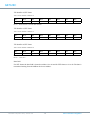
Signals and I/O Switch Matrix
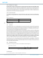
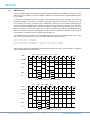
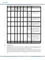
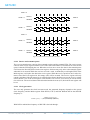
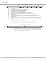
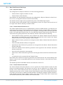
The GR712RC is housed in a 240-pin ceramic quad-flat pack package (CQFP-240). To fit in this
package, some of the on-chip peripheral functions have to share I/O pins. A programmable I/O switch
matrix provides access to several I/O units. When an interface is not activated, its pins automatically
become general purpose I/O. After reset, all I/O switch matrix pins are defined as I/O until programmed otherwise. The programmable I/O switch matrix consists of 67 pins.
Figure 1 shows how the various I/O units are connected to the I/O switch matrix. Table 5 shows examples of possible configurations using the I/O switch matrix. Note that two SpaceWire interfaces are
always available outside the I/O switch matrix.
Table 6 shows a listing of all pins in the I/O switch matrix, indicating the priority amongst them. Note
that some pins are input only, some are output only, and the rest are both input and output, as
described in table 6.
Table 7 shows a listing of pins in the I/O switch matrix grouped per function (GPIO is not listed).
Table 8 shows a complete listing of conflicts between I/O units (GPIO is not listed).
TMS, TCK
TDI, TDO
JTAG
INCLK, SPWCLK
DLLBPN, RESETN
ERRORN
DSU
LEON3FT
LEON3FT 192K RAM CANMUX CLKGATE GPREG
TESTEN
SCANEN
WDOGN
IRQ
STAT
TIMERS
AMBA
TM
MCTRL SDRAM
1553
TC
SLINK
CAN
I2C
ETH
SPI
UART
UART
UART
UART
UART
UART
ASCS
GPIO
GPIO
SPW
SPW
SPW
SPW
SWMX[66:0]
ADDRESS[23:0]
DATA[31:0], CB[7:0]
CTRL, SDCLK
SPW
SPW
SPW_TXD/S[1:0]
SPW_RXD/S[1:0]
Figure 1. Architectural block diagram showing connections to the I/O switch matrix
Table 5. Example of possible configurations using the I/O switch matrix
Interface type
Example configuration
CF0
SDRAM with or without Reed-Solomon
CF1
CF2
CF3
CF4
CF5
1
1
1
1
1
6
UART
6
4
6
6
6
SpaceWire
6
4
2
2
4
3
1
1
Ethernet
CAN
MIL-STD-1553B BC/RT/BM
1
I2C
1
SPI
1
1
SLINK
1
ASCS16
1
CCSDS/ECSS TC & TM
GR712RC-UM, Nov 2015, Version 2.6
1
1
1
1
1
1
1
21
www.combham.com/gaisler
GR712RC
Table 6. I/O switch matrix pin description, defining the order of priority for outputs and input/outputs, with the highest
priority for each pin listed first.
Pin no.
Pin name
Pin function
Polarity
Reset value
Dir.
Description
4
SWMX[0]
UART_TX[0]
-
High
Out
UART Transmit 0
3
SWMX[1]
UART_RX[0]
-
2
SWMX[2]
UART_TX[1]
-
1
SWMX[3]
UART_RX[1]
-
GPIO[0]
-
In
GPIO 1 Register, bit 0 (input only)
240
SWMX[4]
UART_TX[2]
-
High-Z
Out
UART Transmit 2
GPIO[1]
-
High-Z
In/Out
GPIO 1 Register, bit 1
MCFG3[8]
-
In
At reset, bit 8 in MCFG3 register in the memory controller is set from this input.
239
238
233
232
231
230
229
228
227
226
225
220
219
SWMX[5]
SWMX[6]
SWMX[7]
SWMX[8]
SWMX[9]
SWMX[10]
SWMX[11]
SWMX[12]
SWMX[13]
SWMX[14]
SWMX[15]
SWMX[16]
SWMX[17]
High
In
UART Receive 0
Out
UART Transmit 1
In
UART Receive 1
UART_RX[2]
-
In
UART Receive 2
GPIO[2]
-
In
GPIO 1 Register, bit 2 (input only)
UART_TX[3]
-
High-Z
Out
UART Transmit 3
GPIO[3]
-
High-Z
In/Out
GPIO 1 Register, bit 3
MCFG1[9]
-
In
At reset, bit 9 in MCFG1 register in the memory controller is set from this input
UART_RX[3]
-
In
UART Receive 3
GPIO[4]
-
In
GPIO 1 Register, bit 4 (input only)
UART_TX[4]
-
Out
UART Transmit 4
High-Z
TMDO
-
High-Z
Out
Telemetry Data Out
GPIO[5]
-
High-Z
In/Out
GPIO 1 Register, bit 5
UART_RX[4]
-
In
UART Receive 4
TMCLKI
Rising
In
Telemetry Clock Input
GPIO[6]
-
UART_TX[5]
-
High-Z
In
GPIO 1 Register, bit 6 (input only)
Out
UART Transmit 5
TMCLKO
-
High-Z
Out
Telemetry Clock Output
GPIO[7]
-
High-Z
In/Out
GPIO 1 Register, bit 7
UART_RX[5]
-
In
UART Receive 5
TCACT[0]
High
In
Telecommand Active 0
In
GPIO 1 Register, bit 8 (input only)
Out
SpaceWire Transmit Strobe 4
GPIO[8]
-
SPW_TXS[4]
High
High-Z
SDCSN[0]
Low
High-Z
Out
SDRAM Select 0
GPIO[9]
-
High-Z
In/Out
GPIO 1 Register, bit 9
SPW_TXD[4]
High
High-Z
Out
SpaceWire Transmit Data 4
SDCSN[1]
Low
High-Z
Out
SDRAM Select 1
High-Z
GPIO[10]
-
In/Out
GPIO 1 Register, bit 10
SPW_RXS[4]
High
In
SpaceWire Receive Strobe 4
TCCLK[0]
Rising
In
Telecommand Clock 0
A16DASA
-
In
ASCS DAS A - Slave data in
GPIO[11]
-
In
GPIO 1 Register, bit 11 (input only)
SPW_RXD[4]
High
In
SpaceWire Receive Data 4
TCD[0]
-
In
Telecommand Data 0
A16DASB
-
In
ASCS DAS B - Slave data in
In
GPIO 1 Register, bit 12 (input only)
GPIO[12]
-
SPW_TXS[2]
High
High-Z
Out
SpaceWire Transmit Strobe 2
CANTXA
-
High-Z
Out
CAN Transmit A
GPIO[13]
-
High-Z
In/Out
GPIO 1 Register, bit 13
SPW_TXD[2]
High
High-Z
Out
SpaceWire Transmit Data 2
CANTXB
-
High-Z
Out
CAN Transmit B
GPIO[14]
-
High-Z
In/Out
GPIO 1 Register, bit 14
GR712RC-UM, Nov 2015, Version 2.6
22
www.combham.com/gaisler
GR712RC
Table 6. I/O switch matrix pin description, defining the order of priority for outputs and input/outputs, with the highest
priority for each pin listed first.
Pin no.
Pin name
Pin function
Polarity
218
SWMX[18]
SPW_RXS[2]
CANRXA
217
203
202
201
200
197
196
193
192
191
SWMX[19]
SWMX[20]
SWMX[21]
SWMX[22]
SWMX[23]
SWMX[24]
SWMX[25]
SWMX[26]
SWMX[27]
SWMX[28]
Reset value
Dir.
Description
High
In
SpaceWire Receive Strobe 2
-
In
CAN Receive A
GPIO[15]
-
In
GPIO 1 Register, bit 15 (input only)
SPW_RXD[2]
High
In
SpaceWire Receive Data 2
CANRXB
-
In
CAN Receive B
GPIO[16]
-
In
GPIO 1 Register, bit 16 (input only)
SPW_TXS[3]
High
High-Z
Out
SpaceWire Transmit Strobe 3
SLSYNC
High
High-Z
Out
SLINK SYNC
GPIO[17]
-
High-Z
In/Out
GPIO 1 Register, bit 17
SPW_TXD[3]
High
High-Z
Out
SpaceWire Transmit Data 3
A16ETR
High
High-Z
Out
ASCS ETR - Synchronization signal
GPIO[18]
-
High-Z
In/Out
GPIO 1 Register, bit 18
SPW_RXS[3]]
High
In
SpaceWire Receive Strobe 3
GPIO[19]
-
In
GPIO 1 Register, bit 19 (input only)
SPW_RXD[3]
High
In
SpaceWire Receive Data 3
GPIO[20]
-
In
GPIO 1 Register, bit 20 (input only)
SPW_TXD[5]
High
High-Z
Out
SpaceWire Transmit Data 5
SDDQM[0]
High
High-Z
Out
SDRAM Data Mask 0, corresponds to
DATA[7:0]
GPIO[21]
-
High-Z
In/Out
GPIO 1 Register, bit 21
SPW_TXS[5]
High
High-Z
Out
SpaceWire Transmit Strobe 5
SDDQM[1]
High
High-Z
Out
SDRAM Data Mask 1, corresponds to
DATA[15:8]
High-Z
GPIO[22]
-
In/Out
GPIO 1 Register, bit 22
SPW_RXS[5]
High
In
SpaceWire Receive Strobe 5
TCRFAVL[0]
High
In
Telecommand RF Available 0
GPIO[23]
-
In
GPIO 1 Register, bit 23 (input only)
SPW_RXD[5]
High
In
SpaceWire Receive Data 5
TCCLK[1]
Rising
In
Telecommand Clock 1
GPIO[24]
-
In
GPIO 1 Register, bit 24 (input only)
1553RXENA
High
High-Z
Out
MIL-STD-1553B Receive Enable A
High-Z
Out
Proprietary, enabled by CAN
-
190
SWMX[29]
RMTXD[0]
-
High-Z
Out
Ethernet Transmit Data 0
GPIO[25]
-
High-Z
In/Out
GPIO 1 Register, bit 25
1553TXA
High
High-Z
Out
MIL-STD-1553B Transmit Positive A
High-Z
Out
Proprietary, enabled by CAN
-
189
188
185
SWMX[30]
SWMX[31]
SWMX[32]
RMTXD[1]
-
High-Z
Out
Ethernet Transmit Data 1
GPIO[26]
-
High-Z
In/Out
GPIO 1 Register, bit 26
1553RXA
High
In
MIL-STD-1553B Receive Positive A
TCD[1]
-
In
Telecommand Data 1
RMRXD[0]
-
In
Ethernet Receive Data 0
GPIO[27]
-
In
GPIO 1 Register, bit 27 (input only)
1553RXNA
Low
In
MIL-STD-1553B Receive Negative A
TCACT[1]
High
In
Telecommand Active 1
RMRXD[1]
-
In
Ethernet Receive Data 1
GPIO[28]
-
In
GPIO 1 Register, bit 28 (input only)
1553TXNA
Low
High-Z
Out
MIL-STD-1553B Transmit Negative A
High-Z
Out
Proprietary, enabled by CAN
-
184
SWMX[33]
RMTXEN
High
High-Z
Out
Ethernet Transmit Enable
GPIO[29]
-
High-Z
In/Out
GPIO 1 Register, bit 29
1553TXINHA
High
High-Z
Out
MIL-STD-1553B Transmit Inhibit A
GR712RC-UM, Nov 2015, Version 2.6
23
www.combham.com/gaisler
GR712RC
Table 6. I/O switch matrix pin description, defining the order of priority for outputs and input/outputs, with the highest
priority for each pin listed first.
Pin no.
Pin name
Pin function
Polarity
Reset value
High-Z
Out
Proprietary, enabled by CAN
GPIO[30]
-
High-Z
In/Out
GPIO 1 Register, bit 30
1553RXB
High
In
MIL-STD-1553B Receive Positive B
TCRFAVL[1]
High
In
Telecommand RF Available 1
-
183
182
179
178
177
SWMX[34]
SWMX[35]
SWMX[36]
SWMX[37]
SWMX[38]
Dir.
Description
RMCRSDV
High
In
Ethernet Carrier Sense / Data Valid
GPIO[31]
-
In
GPIO 1 Register, bit 31 (input only)
1553RXNB
Low
In
MIL-STD-1553B Receive Negative B
TCCLK[2]
Rising
In
Telecommand Clock 2
RMINTN
Low
In
Ethernet Management Interrupt
GPIO[32]
-
In
GPIO 2 Register, bit 0 (input only)
1553RXENB
High
High-Z
Out
MIL-STD-1553B Receive Enable B
A16MCS
High
High-Z
Out
ASCS MCS - TM start/stop signal
RMMDIO
-
High-Z
In/Out
Ethernet Media Interface Data
GPIO[33]
-
High-Z
In/Out
GPIO 2 Register, bit 1
1553TXB
High
High-Z
Out
MIL-STD-1553B Transmit Positive B
A16HS
High
High-Z
Out
ASCS HS - TM/TC serial clock
RMMDC
-
High-Z
Out
Ethernet Media Interface Clock
GPIO[34]
-
High-Z
In/Out
GPIO 2 Register, bit 2
SpaceWire clock
divisor registers
-
In
At reset, bits 8 and 0 in the clock divisor register of the SpaceWire interfaces are set from
this input
1553CK
-
In
MIL-STD-1553B Clock
TCD[2]
-
In
Telecommand Data 2
RMRFCLK
-
In
Ethernet Reference Clock
GPIO[35]
-
In
GPIO 2 Register, bit 3 (input only)
176
SWMX[39]
TCACT[2]
High
In
Telecommand Active 2
GPIO[36]
-
175
SWMX[40]
1553TXNB
Low
174
173
172
169
166
165
SWMX[41]
SWMX[42]
SWMX[43]
SWMX[44]
SWMX[45]
SWMX[46]
High-Z
In
GPIO 2 Register, bit 4 (input only)
Out
MIL-STD-1553B Transmit Negative B
A16DCS
-
High-Z
Out
ASCS DCS - Slave data out
GPIO[37]
-
High-Z
In/Out
GPIO 2 Register, bit 5
SpaceWire clock
divisor registers
-
In
At reset, bits 9 and 1 in the clock divisor register of the SpaceWire interfaces are set from
this input
1553TXINHB
High
High-Z
Out
MIL-STD-1553B Transmit Inhibit B
A16MAS
High
High-Z
Out
ASCS MAS - TM start/stop signal
GPIO[38]
-
High-Z
In/Out
GPIO 2 Register, bit 6
TCRFAVL[2]
High
In
Telecommand RF Available 2
GPIO[39]
-
In
GPIO 2 Register, bit 7 (input only)
GPIO[40]
-
SpaceWire clock
divisor registers
-
SPICLK
High-Z
Out
Proprietary, enabled by CAN
High-Z
In/Out
GPIO 2 Register, bit 8
In
At reset, bits 10 and 2 in the clock divisor register of the SpaceWire interfaces are set from
this input
SPI Clock
High-Z
Out
SLO
-
High-Z
Out
SLINK Data Out
GPIO[41]
-
High-Z
In/Out
GPIO 2 Register, bit 9
SPIMOSI
-
High-Z
Out
SPI Master Out Slave In
SLCLK
High
High-Z
Out
SLINK Clock
GPIO[42]
-
High-Z
In/Out
GPIO 2 Register, bit 10
SpaceWire clock
divisor registers
-
In
At reset, bits 11 and 3 in the clock divisor register of the SpaceWire interfaces are set from
this input
TCCLK[3]
Rising
In
Telecommand Clock 3
GPIO[43]
-
In
GPIO 2 Register, bit 11 (input only)
GR712RC-UM, Nov 2015, Version 2.6
24
www.combham.com/gaisler
GR712RC
Table 6. I/O switch matrix pin description, defining the order of priority for outputs and input/outputs, with the highest
priority for each pin listed first.
Pin no.
Pin name
Pin function
164
SWMX[47]
TCD[3]
-
In
Telecommand Data 3
GPIO[44]
-
In
GPIO 2 Register, bit 12 (input only)
SDCASN
Low
High-Z
Out
SDRAM Column Address Strobe
GPIO[45]
-
High-Z
In/Out
GPIO 2 Register, bit 13
SDRASN
Low
High-Z
Out
SDRAM Row Address Strobe
GPIO[46]
-
High-Z
In/Out
GPIO 2 Register, bit 14
TCACT[3]
High
In
Telecommand Active 3
GPIO[47]
-
In
GPIO 2 Register, bit 15 (input only)
163
162
161
160
157
155
SWMX[48]
SWMX[49]
SWMX[50]
SWMX[51]
SWMX[52]
SWMX[53]
Polarity
Reset value
SPIMISO
Dir.
Description
In
SPI Master In Slave Out
TCRFAVL[3]
High
In
Telecommand RF Available 3
SLI
-
In
SLINK Data In
GPIO[48]
-
In
GPIO 2 Register, bit 16 (input only)
SDWEN
Low
High-Z
Out
SDRAM Write Enable
GPIO[49]
-
High-Z
In/Out
GPIO 2 Register, bit 17
SDDQM[2]
High
High-Z
Out
SDRAM Data Mask 2, corresponds to
DATA[23:16]
GPIO[50]
-
High-Z
In/Out
GPIO 2 Register, bit 18
154
SWMX[54]
SDDQM[3]
High
High-Z
Out
SDRAM Data Mask 3, corresponds to
DATA[31:24]
GPIO[51]
-
High-Z
In/Out
GPIO 2 Register, bit 19
153
SWMX[55]
TCACT[4]
High
In
Telecommand Active 4
GPIO[52]
-
In
GPIO 2 Register, bit 20 (input only)
TCRFAVL[4]
High
In
Telecommand RF Available 4
GPIO[53]
-
In
GPIO 2 Register, bit 21 (input only)
High-Z
In/Out
I2C Serial Data
High-Z
In/Out
GPIO 2 Register, bit 22
In
Telecommand Clock 4
High-Z
In/Out
I2C Serial Clock
High-Z
In/Out
GPIO 2 Register, bit 23
In
Telecommand Data 4
Reed-Solomon Check Bit 8
144
143
142
140
137
136
135
132
129
128
127
SWMX[56]
SWMX[57]
SWMX[58]
SWMX[59]
SWMX[60]
SWMX[61]
SWMX[62]
SWMX[63]
SWMX[64]
SWMX[65]
SWMX[66]
I2CSDA
GPIO[54]
-
TCCLK[4]
Rising
I2CSCL
GPIO[55]
-
TCD[4]
-
CB[8]
-
High-Z
In/Out
GPIO[56]
-
High-Z
In/Out
GPIO 2 Register, bit 24
CB[9]
-
High-Z
In/Out
Reed-Solomon Check Bit 9
GPIO[57]
-
High-Z
In/Out
GPIO 2 Register, bit 25
CB[10]
-
High-Z
In/Out
Reed-Solomon Check Bit 10
GPIO[58]
-
High-Z
In/Out
GPIO 2 Register, bit 26
CB[11]
-
High-Z
In/Out
Reed-Solomon Check Bit 11
GPIO[59]
-
High-Z
In/Out
GPIO 2 Register, bit 27
CB[12]
-
High-Z
In/Out
Reed-Solomon Check Bit 12
GPIO[60]
-
High-Z
In/Out
GPIO 2 Register, bit 28
CB[13]
-
High-Z
In/Out
Reed-Solomon Check Bit 13
GPIO[61]
-
High-Z
In/Out
GPIO 2 Register, bit 29
CB[14]
-
High-Z
In/Out
Reed-Solomon Check Bit 14
GPIO[62]
-
High-Z
In/Out
GPIO 2 Register, bit 30
CB[15]
-
High-Z
In/Out
Reed-Solomon Check Bit 15
GPIO[63]
-
High-Z
In/Out
GPIO 2 Register, bit 31
GR712RC-UM, Nov 2015, Version 2.6
25
www.combham.com/gaisler
GR712RC
Table 7. I/O switch matrix pins listed per function, including supporting signals outside the I/O switch matrix.
Pin no.
Pin name
Pin function
Polarity
Reset value
Dir.
Description
157
SWMX[52]
SDWEN
Low
High-Z
Out
SDRAM Write Enable
163
SWMX[48]
SDCASN
Low
High-Z
Out
SDRAM Column Address Strobe
162
SWMX[49]
SDRASN
Low
High-Z
Out
SDRAM Row Address Strobe
228
SWMX[12]
SDCSN[0]
Low
High-Z
Out
SDRAM Select 0
227
SWMX[13]
SDCSN[1]
Low
High-Z
Out
SDRAM Select 1
197
SWMX[24]
SDDQM[0]
High
High-Z
Out
SDRAM Data Mask 0, corresponds to
DATA[7:0]
196
SWMX[25]
SDDQM[1]
High
High-Z
Out
SDRAM Data Mask 1, corresponds to
DATA[15:8]
155
SWMX[53]
SDDQM[2]
High
High-Z
Out
SDRAM Data Mask 2, corresponds to
DATA[23:16]
154
SWMX[54]
SDDQM[3]
High
High-Z
Out
SDRAM Data Mask 3, corresponds to
DATA[31:24]
140
SWMX[59]
CB[8]
-
High-Z
In/Out
Check Bit 8, Reed-Solomon
137
SWMX[60]
CB[9]
-
High-Z
In/Out
Check Bit 9, Reed-Solomon
136
SWMX[61]
CB[10]
-
High-Z
In/Out
Check Bit 10, Reed-Solomon
135
SWMX[62]
CB[11]
-
High-Z
In/Out
Check Bit 11, Reed-Solomon
132
SWMX[63]
CB[12]
-
High-Z
In/Out
Check Bit 12, Reed-Solomon
129
SWMX[64]
CB[13]
-
High-Z
In/Out
Check Bit 13, Reed-Solomon
128
SWMX[65]
CB[14]
-
High-Z
In/Out
Check Bit 14, Reed-Solomon
127
SWMX[66]
CB[15]
-
High-Z
In/Out
Check Bit 15, Reed-Solomon
ADDRESS[16:2]
ADDRESS[16:2]
-
Low
Out
Memory address
DATA[31:0]
DATA[31:0]
-
High-Z
In/Out
Memory data bus
High-Z
CB[7:0]
CB[7:0]
-
In/Out
Memory checkbits
240
SWMX[4]
MCFG3[8]
-
In
At reset, bit 8 in MCFG3 register in the
memory controller is set from this input.
238
SWMX[6]
MCFG1[9]
-
In
At reset, bit 9 in MCFG1 register in the
memory controller is set from this input
4
SWMX[0]
UART_TX[0]
-
High
Out
UART Transmit 0
3
SWMX[1]
UART_RX[0]
-
In
UART Receive 0
2
SWMX[2]
UART_TX[1]
-
High
Out
UART Transmit 1
1
SWMX[3]
UART_RX[1]
-
In
UART Receive 1
240
SWMX[4]
UART_TX[2]
-
High-Z
Out
UART Transmit 2
In
UART Receive 2
High-Z
Out
UART Transmit 3
In
UART Receive 3
High-Z
Out
UART Transmit 4
In
UART Receive 4
High-Z
Out
UART Transmit 5
239
SWMX[5]
UART_RX[2]
-
238
SWMX[6]
UART_TX[3]
-
233
SWMX[7]
UART_RX[3]
-
232
SWMX[8]
UART_TX[4]
-
231
SWMX[9]
UART_RX[4]
-
230
SWMX[10]
UART_TX[5]
-
229
SWMX[11]
UART_RX[5]
-
In
UART Receive 5
213
SPW_RXD[0]
SPW_RXD[0]
High
In
SpaceWire Receive Data 0
214
SPW_RXS[0]
SPW_RXS[0]
High
In
SpaceWire Receive Strobe 0
215
SPW_TXD[0]
SPW_TXD[0]
High
Low
Out
SpaceWire Transmit Data 0
216
SPW_TXS[0]
SPW_TXS[0]
High
Low
Out
SpaceWire Transmit Strobe 0
204
SPW_RXD[1]
SPW_RXD[1]
High
In
SpaceWire Receive Data 1
205
SPW_RXS[1]
SPW_RXS[1]
High
In
SpaceWire Receive Strobe 1
206
SPW_TXD[1]
SPW_TXD[1]
High
Low
Out
SpaceWire Transmit Data 1
209
SPW_TXS[1]
SPW_TXS[1]
High
Low
Out
SpaceWire Transmit Strobe 1
217
SWMX[19]
SPW_RXD[2]
High
In
SpaceWire Receive Data 2
218
SWMX[18]
SPW_RXS[2]
High
219
SWMX[17]
SPW_TXD[2]
High
High-Z
220
SWMX[16]
SPW_TXS[2]
High
High-Z
Out
SpaceWire Transmit Strobe 2
200
SWMX[23]
SPW_RXD[3]
High
In
SpaceWire Receive Data 3
201
SWMX[22]
SPW_RXS[3]
High
In
SpaceWire Receive Strobe 3
GR712RC-UM, Nov 2015, Version 2.6
26
In
SpaceWire Receive Strobe 2
Out
SpaceWire Transmit Data 2
www.combham.com/gaisler
GR712RC
Table 7. I/O switch matrix pins listed per function, including supporting signals outside the I/O switch matrix.
Pin no.
Pin name
Pin function
Polarity
Reset value
Dir.
Description
202
SWMX[21]
SPW_TXD[3]
High
High-Z
Out
SpaceWire Transmit Data 3
203
SWMX[20]
SPW_TXS[3]
High
High-Z
225
SWMX[15]
SPW_RXD[4]
High
226
SWMX[14]
SPW_RXS[4]
High
227
SWMX[13]
SPW_TXD[4]
High
High-Z
228
SWMX[12]
SPW_TXS[4]
High
High-Z
192
SWMX[27]
SPW_RXD[5]
High
Out
SpaceWire Transmit Strobe 3
In
SpaceWire Receive Data 4
In
SpaceWire Receive Strobe 4
Out
SpaceWire Transmit Data 4
Out
SpaceWire Transmit Strobe 4
In
SpaceWire Receive Data 5
193
SWMX[26]
SPW_RXS[5]
High
In
SpaceWire Receive Strobe 5
197
SWMX[24]
SPW_TXD[5]
High
High-Z
Out
SpaceWire Transmit Data 5
196
SWMX[25]
SPW_TXS[5]
High
High-Z
Out
SpaceWire Transmit Strobe 5
178
SWMX[37]
-
In
At reset, bits 8 & 0 are set from this input
175
SWMX[40]
-
In
At reset, bits 9 & 1 are set from this input
172
SWMX[43]
SpaceWire clock
divisor registers
values at reset, all
other bits are zero.
-
In
At reset, bits 10 & 2 are set from this input
166
SWMX[45]
-
In
At reset, bits 11 & 3 are set from this input
185
SWMX[32]
RMTXEN
High
High-Z
Out
Ethernet Transmit Enable
191
SWMX[28]
RMTXD[0]
-
High-Z
Out
Ethernet Transmit Data 0
190
SWMX[29]
RMTXD[1]
-
High-Z
Out
Ethernet Transmit Data 1
189
SWMX[30]
RMRXD[0]
-
In
Ethernet Receive Data 0
188
SWMX[31]
RMRXD[1]
-
In
Ethernet Receive Data 1
183
SWMX[34]
RMCRSDV
High
In
Ethernet Carrier Sense / Data Valid
182
SWMX[35]
RMINTN
Low
In
Ethernet Management Interrupt
179
SWMX[36]
RMMDIO
-
High-Z
In/Out
Ethernet Media Interface Data
178
SWMX[37]
RMMDC
-
High-Z
Out
Ethernet Media Interface Clock
In
Ethernet Reference Clock
High-Z
Out
CAN Transmit A
In
CAN Receive A
High-Z
Out
CAN Transmit B
177
SWMX[38]
RMRFCLK
-
220
SWMX[16]
CANTXA
-
218
SWMX[18]
CANRXA
-
219
SWMX[17]
CANTXB
-
217
SWMX[19]
CANRXB
-
In
CAN Receive B
191
SWMX[28]
-
High-Z
Out
Proprietary, enabled by CAN
190
SWMX[29]
-
High-Z
Out
Proprietary, enabled by CAN
185
SWMX[32]
-
High-Z
Out
Proprietary, enabled by CAN
184
SWMX[33]
-
High-Z
Out
Proprietary, enabled by CAN
172
SWMX[43]
-
High-Z
Out
Proprietary, enabled by CAN
177
SWMX[38]
1553CK
-
In
MIL-STD-1553B Clock
184
SWMX[33]
1553TXINHA
High
High-Z
Out
MIL-STD-1553B Transmit Inhibit A
190
SWMX[29]
1553TXA
High
High-Z
Out
MIL-STD-1553B Transmit Positive A
185
SWMX[32]
1553TXNA
Low
High-Z
Out
MIL-STD-1553B Transmit Negative A
191
SWMX[28]
1553RXENA
High
High-Z
Out
MIL-STD-1553B Receive Enable A
189
SWMX[30]
1553RXA
High
In
MIL-STD-1553B Receive Positive A
188
SWMX[31]
1553RXNA
Low
In
MIL-STD-1553B Receive Negative A
174
SWMX[41]
1553TXINHB
High
High-Z
Out
MIL-STD-1553B Transmit Inhibit B
178
SWMX[37]
1553TXB
High
High-Z
Out
MIL-STD-1553B Transmit Positive B
175
SWMX[40]
1553TXNB
Low
High-Z
Out
MIL-STD-1553B Transmit Negative B
179
SWMX[36]
1553RXENB
High
High-Z
Out
MIL-STD-1553B Receive Enable B
183
SWMX[34]
1553RXB
High
In
MIL-STD-1553B Receive Positive B
182
SWMX[35]
1553RXNB
Low
In
MIL-STD-1553B Receive Negative B
143
SWMX[57]
I2CSDA
In/Out
I2C Serial Data
High-Z
142
SWMX[58]
I2CSCL
High-Z
In/Out
I2C Serial Clock
169
SWMX[44]
SPICLK
High-Z
Out
SPI Clock
166
SWMX[45]
SPIMOSI
160
SWMX[51]
SPIMISO
GR712RC-UM, Nov 2015, Version 2.6
-
High-Z
27
Out
SPI Master Out Slave In
In
SPI Master In Slave Out
www.combham.com/gaisler
GR712RC
Table 7. I/O switch matrix pins listed per function, including supporting signals outside the I/O switch matrix.
Pin no.
Pin name
Pin function
Polarity
Reset value
Dir.
Description
203
SWMX[20]
SLSYNC
High
High-Z
Out
SLINK SYNC
166
SWMX[45]
SLCLK
High
High-Z
Out
SLINK Clock
160
SWMX[51]
SLI
-
In
SLINK Data In
169
SWMX[44]
SLO
-
226
SWMX[14]
A16DASA
-
High-Z
Out
SLINK Data Out
In
ASCS DAS A - Slave data in
225
SWMX[15]
A16DASB
-
In
ASCS DAS B - Slave data in
202
SWMX[21]
A16ETR
High
High-Z
Out
ASCS ETR - Synchronization signal
175
SWMX[40]
A16DCS
-
High-Z
Out
ASCS DCS - Slave data out
174
SWMX[41]
A16MAS
High
High-Z
Out
ASCS MAS - TM start/stop signal
179
SWMX[36]
A16MCS
High
High-Z
Out
ASCS MCS - TC start/stop signal
178
SWMX[37]
A16HS
High
High-Z
Out
ASCS HS - TM/TC serial clock
229
SWMX[11]
TCACT[0]
High
In
Telecommand Active 0
226
SWMX[14]
TCCLK[0]
Rising
In
Telecommand Clock 0
225
SWMX[15]
TCD[0]
-
In
Telecommand Data 0
193
SWMX[26]
TCRFAVL[0]
High
In
Telecommand RF Available 0
188
SWMX[31]
TCACT[1]
High
In
Telecommand Active 1
192
SWMX[27]
TCCLK[1]
Rising
In
Telecommand Clock 1
189
SWMX[30]
TCD[1]
-
In
Telecommand Data 1
183
SWMX[34]
TCRFAVL[1]
High
In
Telecommand RF Available 1
176
SWMX[39]
TCACT[2]
High
In
Telecommand Active 2
182
SWMX[35]
TCCLK[2]
Rising
In
Telecommand Clock 2
177
SWMX[38]
TCD[2]
-
In
Telecommand Data 2
173
SWMX[42]
TCRFAVL[2]
High
In
Telecommand RF Available 2
161
SWMX[50]
TCACT[3]
High
In
Telecommand Active 3
165
SWMX[46]
TCCLK[3]
Rising
In
Telecommand Clock 3
164
SWMX[47]
TCD[3]
-
In
Telecommand Data 3
160
SWMX[51]
TCRFAVL[3]
High
In
Telecommand RF Available 3
153
SWMX[55]
TCACT[4]
High
In
Telecommand Active 4
143
SWMX[57]
TCCLK[4]
Rising
In
Telecommand Clock 4
142
SWMX[58]
TCD[4]
-
In
Telecommand Data 4
144
SWMX[56]
TCRFAVL[4]
High
In
Telecommand RF Available 4
231
SWMX[9]
TMCLKI
Rising
In
Telemetry Clock Input
230
SWMX[10]
TMCLKO
-
High-Z
Out
Telemetry Clock Output
232
SWMX[8]
TMDO
-
High-Z
Out
Telemetry Data Out
GR712RC-UM, Nov 2015, Version 2.6
28
www.combham.com/gaisler
GR712RC
Table 8. Conflicting interfaces in the I/O switch matrix are marked with an X, with duplicates shown in bold typeface.
-
UART 0
X
X
-
UART 1
-
UART 2
-
UART 3
-
UART 4
-
UART 5
X
-
SpaceWire 0
X
X
-
SpaceWire 1
-
SpaceWire 2
-
X
SpaceWire 3
X
-
SpaceWire 5
X
-
X
-
Ethernet
CAN
X
MIL-STD-1553B
X
X
-
X
X
-
X
X
-
I2C
X
X
X
X
X
X
-
SPI
SLINK
X
ASCS
X
CCSDS TC 0
X
X
X
-
X
X
-
X
X
X
CCSDS TC 1
X
CCSDS TC 2
X
X
X
X
X
-
X
X
-
CCSDS TC 3
X
X
-
CCSDS TC 3
CCSDS TC 2
CCSDS TC 1
CCSDS TC 0
ASCS
SLINK
I2C
MIL-STD-1553B
CAN
Ethernet
SpaceWire 5
SpaceWire 4
SpaceWire 3
SpaceWire 2
-
SpaceWire 1
X
SpaceWire 0
UART 3
UART 2
UART 1
UART 0
SDRAM (with RS)
X
UART 5
X
CCSDS TM
UART 4
CCSDS TC 4
X
CCSDS TM
X
CCSDS TC 4
SpaceWire 4
X
SPI
SDRAM (with RS)
Which peripheral function that drives a shared I/O pin is determined through a set of enabling conditions. Peripheral functions that are clock gated use the clock enable bit as I/O matrix select signal.
Enabling conditions for peripherals without clock gating are defined in table 9.
TABLE 9. I/O switch matrix enables for non-gated devices
Device
Enable
UART
TX enable bit in APBUART control register
SPI
Enable bit in SPICTRL control register
I2C
Enable bit in I2CMST control register
ASCS
Output enable bit in GRASCS control register
SLINK
Enable bit in SLINKMST control register
SDRAM
SDRAM enable in MCFG2
RS checkbits
Reed-Solomon enable in MCFG3
The peripherals are connected to the switch matrix I/O pin through a priority structure that makes sure
only one peripheral is granted the pin at a time. If no device is enabled, the pin defaults to the respective GPIO[63:0]. Note that there are two GRGPIO cores each with 32 bits, thus only 64 of the 67 pins
have a GPIO pin alternative. The first GRGPIO core is mapped on GPIO[31:0], and the second GPIO
core is mapped on GPIO[63:32]. Also note that when the CAN core is enabled, the output of pins 172,
GR712RC-UM, Nov 2015, Version 2.6
29
www.combham.com/gaisler
GR712RC
184, 185, 190 and 191 will be driven with random values. These pins are shared with the Mil-Std1553 interface, but since this interface has a higher priority, the two interfaces are not considered conflicting in the case they are both enabled simultaneously.
The pins listed in table 10 have fixed functions that are not connected to the switch matrix.
TABLE 10. GR712RC fixed pins
Interface
GR712RC pin
Miscellaneous
ERRORN
In
Total
1
INCLK
1
1
RESETN
1
1
DLLBPN
1
1
TESTEN
1
1
SCANEN
1
1
1
TDI
1
1
TDO
Memory interface
In/Out
1
WDOGN
JTAG
Out
1
1
TMS
1
TCK
1
ADDRESS[23:0]
1
1
1
24
DATA[31:0]
24
32
Control (READ, BRDYN, BEXCN)
2
1
Check bits (CB[7:0])
32
3
8
8
SRAM control (RAMSN[1:0], RAMOEN, RAMWEN)
4
4
PROM control (ROMSN[1:0], OEN, WRITEN)
4
4
I/O control (IOSN)
1
1
1
1
SDRAM clock (SDCLK)
SpaceWire 0-1
SpaceWire receiver and transmitter clock (SPWCLK)
1
(with RMAP)
SpaceWire 0-1 receive/transmit data/strobe
4
4
15
42
Number of pins
GR712RC-UM, Nov 2015, Version 2.6
30
1
8
40
97
www.combham.com/gaisler
GR712RC
3
Clocking
The table below specifies the clock inputs to the GR712RC.
TABLE 11. Clock inputs
Clock input
Description
INCLK
System clock input
SPWCLK
SpaceWire clock
TMCLKI
Telemetry transponder clock (input shared with UART4)
1553CK
1553 clock (input shared with Ethernet and TC)
RMRFCLK
Ethernet RMII clock (input shared with 1553 and TC)
The design makes use of two MFDLL clock multipliers to create the system clock and the SpaceWire
transmitter clock. The system clock (AHB clock), the SpaceWire transmitter clock and the 1553 clock
is connected through clock multiplexers in order to select between a number of clock options
described below.
3.1
System clock
The system clock is used to clock the processors, the AMBA buses, and all on-chip cores. The system
clock is either taken from the INCLK input, or from a MFDLL clock multiplier providing 2x INCLK.
The DLLBPN input is used to select system clock source.
INCLK
0
MFDLL
2X
System clock (CLK)
1
DLLBPN
3.2
SpaceWire clock
The clock source for SpaceWire is selectable through a clock multiplexer, whose inputs are SPWCLK, and INCLK. The selected clock is then used either as 1X, 2X or 4X as shown in the figure
below. The system clock (CLK) is also selectable as SpaceWire transmit clock.
SPWCLK
INCLK
CLK
1X
2X
MFDLL
SpaceWire TX clock
4X
After reset the selected SpaceWire transmit clock is SPWCLK without any multiplication. The SpaceWire clock multiplexers and the DLL reset are controlled through the GRGPREG register.
The SpaceWire transmit clock must be a multiple of 10 MHz in order to achieve 10 Mbps start up bit
rate. The division to 10 MHz is done internally in the GRSPW2 core. During reset the clock divider
register in GRSPW2 gets its value from 4 I/O pins that must be pulled up/down to set the divider correctly. Pins (MSB-LSB) SWMX45, 43, 40 and 37 are used for this. Thus it is possible to use a SPW-
GR712RC-UM, Nov 2015, Version 2.6
31
www.combham.com/gaisler
GR712RC
CLK which is any multiple of 10 between 10-100 MHz (note that the required precision is 10 MHz +/
- 1 MHz).
The SpaceWire transmitter uses SDR output registers meaning that the bitrate will be equal to the
transmit clock. The SpaceWire input signals are sampled synchronously with DDR registers using the
transmit clock.
3.3
MIL-STD-1553
The B1553BRM core needs a 24, 20 or 16 MHz clock. The frequency used can be configured through
a register in the core. This clock can either be supplied directly to the B1553BRM core through the
1553CK pin, the system clock, or it can be generated through a clock divider that divides the system
clock and is programmable through the GPREG.
If the system clock is used to generate the BRM clock it must be one of the frequencies in the table
below:
Table 12. MIL-STD-1553 BRM frequencies
System clock (MHz)
Division
BRM frequency (MHz)
32
2
16 2)
40
2
20
48
2
24
64
4
16
80
4
20
96
4
24
120
6
20
144
6
24
Note 1: The system clock frequency must always be higher than BRM clock frequency, regardless of
how the BRM clock is generated.
Note 2: This specific case has not been validated.
3.4
Telemetry
The telemetry input clock frequency must be less than or equal to the system clock frequency. It is
possible to select either TMCLKI or system clock as input clock to the GRTM core.
The TMDO data signal is timed relative to TMCLKO.
3.5
Telecommand
The telecommand input signals are sampled using the system clock and the telecommand input clock
frequency must be less than or equal to the system clock frequency divided by eight.
3.6
Obsolete
Proprietary function not supported.
3.7
SLINK
The SLINK core is clocked by the system clock and has a built in clock divider. When using this interface the system clock must be a multiple of 12 MHz if a 50% duty cycle is necessary. If the SLINK
clock duty cycle does not need to be 50% any multiple of 6 MHz is possible.
GR712RC-UM, Nov 2015, Version 2.6
32
www.combham.com/gaisler
GR712RC
3.8
SDRAM clock
The SDRAM clock (SDCLK) output is driven from the internal system clock. A programmable delay
line allows tuning the SDCLK phase relative to the internal clock. The output is tuned to be in phase
with the internal clock tree when the delay line is set to zero. If the system clock is generated by the 2x
MFDLL, SDCLK is not active when the reset input (RESETN) is asserted. When the system clock is
generated directly from INCLK (i.e. when DLLBPN = 0), then SDCLK is driven directly from
INCLK passing through the Delay line.
Delay line
System clock (CLK)
SDCLK
SDDELAY
Memory
Controller
Ctrl, Write data
Read data
3.9
Clock gating unit
The GR712RC device has a clock gating unit through which individual cores can have their AHB
clocks enabled/disabled and resets driven. The cores connected to the clock gating unit are listed in
the table below:
Table 13. Devices with gatable clock
Device
Ethernet
SpaceWire 0
SpaceWire 1
SpaceWire 2
SpaceWire 3
SpaceWire 4
SpaceWire 5
CAN 0 - 1
Proprietary
CCSDS Telemetry
CCSDS Telecommand
MIL-STD-1553
LEON3FT (0)
LEON3FT (1)
GRFPU(0)
GRFPU(1)
GR712RC-UM, Nov 2015, Version 2.6
33
www.combham.com/gaisler
GR712RC
The LEON3FT processor cores will automatically be clock gated when the processor enter powerdown or halt state. The floating-point units (GRFPU) will be clock gated when the corresponding processor have disabled FPU operations by setting the %psr.ef bit to zero, or when the processor have
entered power-down/halt mode. For more information see the chapter about the clock gating unit.
3.10
Test mode clocking
When in test mode (TESTEN signal = 1) all clocks in the design are connected to the INCLK test
clock.
GR712RC-UM, Nov 2015, Version 2.6
34
www.combham.com/gaisler
GR712RC
4
LEON3FT - High-performance SPARC V8 32-bit Processor
4.1
Overview
The GR712RC implements two LEON3FT processor cores in SMP configuration. LEON3FT is a 32bit processor core conforming to the IEEE-1754 (SPARC V8) architecture. It is designed for embedded applications, combining high performance with low complexity and low power consumption.
The LEON3FT core has the following main features: 7-stage pipeline with Harvard architecture, separate instruction and data caches, hardware multiplier and divider, on-chip debug support and multiprocessor extensions.
3-Port Register File
Trace Buffer
IEEE-754 FPU
Co-Processor
7-Stage
Integer pipeline
HW MUL/DIV
I-Cache
ITLB
Debug port
Debug support unit
Interrupt port
Interrupt controller
D-Cache
SRMMU
DTLB
AHB I/F
AMBA AHB Master (32-bit)
Figure 2. LEON3 processor core block diagram
4.1.1
Integer unit
The LEON3 integer unit implements the full SPARC V8 standard, including hardware multiply and
divide instructions. The number of register windows is 8. The pipeline consists of 7 stages with a separate instruction and data cache interface (Harvard architecture).
4.1.2
Cache sub-system
Each processor is configured with a 16 KiB instruction cache and a 16 KiB data cache. The instruction cache uses streaming during line-refill to minimize refill latency. The data cache uses writethrough policy and implements a double-word write-buffer. The data cache can also perform bussnooping on the AHB bus.
4.1.3
Floating-point unit
Each LEON3 processor is connected to a unique GRFPU floating-point unit. The GRFPU implements
the IEEE-754 floating-point format and supports both single and double-precision operands.
4.1.4
Memory management unit
A SPARC V8 Reference Memory Management Unit (SRMMU) is provided per processor. The
SRMMU implements the full SPARC V8 MMU specification, and provides mapping between multiple 32-bit virtual address spaces and 32-bit physical memory. A three-level hardware table-walk is
implemented, and the MMU is configured with 32 fully associative TLB entries.
GR712RC-UM, Nov 2015, Version 2.6
35
www.combham.com/gaisler
GR712RC
4.1.5
On-chip debug support
The LEON3 pipeline includes functionality to allow non-intrusive debugging on target hardware.
Through the JTAG debug support interface, full access to all processor registers and caches is provided. The debug interfaces also allows single stepping, instruction tracing and hardware breakpoint/
watchpoint control. An internal trace buffer can monitor and store executed instructions, which can
later be read out over the debug interface.
4.1.6
Interrupt interface
LEON3 supports the SPARC V8 interrupt model with a total of 15 asynchronous interrupts. The interrupt interface provides functionality to both generate and acknowledge interrupts. The GR712RC
contains an interrupt controller that support 31 system interrupts, mapped on the 15 processor interrupts.
4.1.7
AMBA interface
The cache system implements an AMBA AHB master to load and store data to/from the caches. The
interface is compliant with the AMBA-2.0 standard. During line refill, incremental burst are generated to optimise the data transfer.
4.1.8
Power-down mode
The LEON3 processor core implements a power-down mode, which halts the pipeline and caches
until the next interrupt using clock gating. This is an efficient way to minimize power-consumption
when the application is idle or when one of the processor cores is not used.
4.1.9
Multi-processor support
LEON3 is designed to be use in multi-processor systems and the GR712RC contains two cores. Each
processor has a unique index to allow processor enumeration. The write-through caches and snooping
mechanism guarantees memory coherency in shared-memory systems.
4.1.10 Fault-tolerance
LEON3FT contains logic to correct up to 4 bit errors per 32-bit cache word and associated tag. The
processor registers are protected by a SEC/DED BCH EDAC.
4.1.11 Performance
Using gcc-4.4.2, a dhrystone figure of 1.34 DMIPS/MHz can be achieved.
4.2
LEON3 integer unit
4.2.1
Overview
The LEON3 integer unit implements the integer part of the SPARC V8 instruction set. The implementation is focused on high performance and low complexity. The LEON3 integer unit has the following
main features:
•
7-stage instruction pipeline
•
Separate instruction and data cache interface
•
8 register windows
•
16-bit Hardware multiplier and Radix-2 divider (non-restoring)
•
Single-vector trapping for reduced code size
GR712RC-UM, Nov 2015, Version 2.6
36
www.combham.com/gaisler
GR712RC
Figure 3 shows a block diagram of the integer unit.
call/branch address
I-cache
+1
Add
‘0’ jmpa tbr
data address
f_pc
Fetch
d_inst
d_pc
r_inst
r_pc
Decode
r_imm
rd
register file
rs1
rs2
imm
Register Access
y, tbr, wim, psr
e_inst
e_pc
rs1
Execute
operand2
alu/shift
m_inst
mul/div
y
e pc
m_pc
result
30
jmpl address
32
32
address/dataout
datain
m_y
Memory
x_inst
x_pc
xres
x_y
w_inst
w_pc
wres
Y
D-cache
Exception
Write-back
30
tbr, wim, psr
Figure 3. LEON3 integer unit datapath diagram
4.2.2
Instruction pipeline
The LEON integer unit uses a single instruction issue pipeline with 7 stages:
1.
FE (Instruction Fetch): If the instruction cache is enabled, the instruction is fetched from the
instruction cache. Otherwise, the fetch is forwarded to the memory controller. The instruction is
valid at the end of this stage and is latched inside the IU.
2.
DE (Decode): The instruction is decoded and the CALL/Branch target addresses are generated.
3.
RA (Register access): Operands are read from the register file or from internal data bypasses.
4.
EX (Execute): ALU operations are performed. For memory operations (e.g., LD) and for JMPL/
RETT, the address is generated.
5.
ME (Memory): Data cache is accessed. Store data is written to the data cache at this time.
6.
XC (Exception) Traps and interrupts are resolved. For cache reads, the data is aligned.
7.
WR (Write): The result of any ALU or cache operations are written back to the register file.
GR712RC-UM, Nov 2015, Version 2.6
37
www.combham.com/gaisler
GR712RC
Table 14 lists the cycles per instruction (assuming cache hit and no icc or load interlock):
Table 14. Instruction timing
Instruction
Clock Cycles
JMPL, RETT
3
Double load
2
Single store
2
Double store
3
SMUL/UMUL
4
SDIV/UDIV
35
Taken Trap
5
Atomic load/store
3
All other instructions
1
4.2.3
SPARC Implementor’s ID
Gaisler Research is assigned number 15 (0xF) as SPARC implementor’s identification. This value is
hard-coded into bits 31:28 in the %psr register. The version number for LEON3 is 3, which is hardcoded in to bits 27:24 of the %psr.
4.2.4
Divide instructions
Full support for SPARC V8 divide instructions is provided (SDIV, UDIV, SDIVCC & UDIVCC). The
divide instructions perform a 64-by-32 bit divide and produce a 32-bit result. Rounding and overflow
detection is performed as defined in the SPARC V8 standard.
GR712RC-UM, Nov 2015, Version 2.6
38
www.combham.com/gaisler
GR712RC
4.2.5
Multiply instructions
The LEON processor supports the SPARC integer multiply instructions UMUL, SMUL UMULCC
and SMULCC. These instructions perform a 32x32-bit integer multiply, producing a 64-bit result.
SMUL and SMULCC performs signed multiply while UMUL and UMULCC performs unsigned
multiply. UMULCC and SMULCC also set the condition codes to reflect the result. The multiply
instructions are performed using a 16x16 hardware multiplier which is iterated four times. To improve
the timing, the 16x16 multiplier is provided with a pipeline stage.
4.2.6
Hardware breakpoints
The integer unit includes two hardware breakpoints. Each breakpoint consists of a pair of applicationspecific registers (%asr24/25 and %asr26/27), one with the break address and one with a mask:
31
2
%asr24, %asr26
WADDR[31:2]
31
WMASK[31:2]
0
IF
2
%asr25, %asr27
1
0
DL DS
Figure 4. Watch-point registers
Any binary aligned address range can be watched - the range is defined by the WADDR field, masked
by the WMASK field (WMASK[x] = 1 enables comparison). On a breakpoint hit, trap 0x0B is generated. By setting the IF, DL and DS bits, a hit can be generated on instruction fetch, data load or data
store. Clearing these three bits will effectively disable the breakpoint function.
4.2.7
Instruction trace buffer
The instruction trace buffer consists of a circular buffer that stores executed instructions. The trace
buffer operation is controlled through the debug support interface, and does not affect processor operation. The size of the trace buffer is 4 KiB, equivalent to 256 lines. The trace buffer is 128 bits wide,
and stores the following information:
•
Instruction address and opcode
•
Instruction result
•
Load/store data and address
•
Trap information
•
30-bit time tag
The operation and control of the trace buffer is further described in section 9.4. Note that in
GR712RC, each processor has its own trace buffer allowing simultaneous tracing of both instruction
streams.
GR712RC-UM, Nov 2015, Version 2.6
39
www.combham.com/gaisler
GR712RC
4.2.8
Processor configuration register
The application specific register 17 (%asr17) provides information on how various configuration
options were set during synthesis. This can be used to enhance the performance of software, or to support enumeration in multi-processor systems. The register can be accessed through the RDASR
instruction, and has the following layout:
31
%asr17
28
INDEX
14 13 12 11 10 9
RESERVED
DW SV 0
10
0
8
1
7
010
5 4
0
00111
Figure 5. LEON3 configuration register (%asr17)
Field Definitions:
[31:28]: Processor index. In multi-processor systems, each LEON core gets a unique index to support enumeration. The
value in this field is 0 for core0 and 1 for core1.
[14]:
Disable write error trap (DWT). When set, a write error trap (tt = 0x2b) will be ignored. Set to zero after reset.
[13]:
Single-vector trapping (SVT) enable. If set, will enable single-vector trapping. Set to zero after reset.
[11:10]: FPU option. Hardcoded to 2 (GRFPU)
[8]:
If set, the SPARC V8 multiply and divide instructions are available. Hardcoded to 1.
[7:5]:
Number of implemented watchpoints. Hardcoded to 2
[4:0]:
Number of implemented registers windows corresponds to NWIN+1. Hardcoded to 7.
GR712RC-UM, Nov 2015, Version 2.6
40
www.combham.com/gaisler
GR712RC
4.2.9
Exceptions
LEON3 adheres to the general SPARC V8 trap model. The table below shows the implemented traps
and their individual priority. When PSR (processor status register) bit ET=0, an exception trap causes
the processor to halt execution and enter error mode, and the external error signal will then be
asserted.
Table 15. Trap allocation and priority
Trap
TT
Pri
Description
reset
0x00
1
Power-on reset
write error
0x2b
2
write buffer error
instruction_access_error
0x01
3
Error during instruction fetch
illegal_instruction
0x02
5
UNIMP or other un-implemented instruction
privileged_instruction
0x03
4
Execution of privileged instruction in user mode
fp_disabled
0x04
6
FP instruction while FPU disabled
cp_disabled
0x24
6
CP instruction while Co-processor disabled
watchpoint_detected
0x0B
7
Hardware breakpoint match
window_overflow
0x05
8
SAVE into invalid window
window_underflow
0x06
8
RESTORE into invalid window
register_hadrware_error
0x20
9
Uncorrectable register file EDAC error
mem_address_not_aligned
0x07
10
Memory access to un-aligned address
fp_exception
0x08
11
FPU exception
data_access_exception
0x09
13
Access error during load or store instruction
tag_overflow
0x0A
14
Tagged arithmetic overflow
divide_exception
0x2A
15
Divide by zero
interrupt_level_1
0x11
31
Asynchronous interrupt 1
interrupt_level_2
0x12
30
Asynchronous interrupt 2
interrupt_level_3
0x13
29
Asynchronous interrupt 3
interrupt_level_4
0x14
28
Asynchronous interrupt 4
interrupt_level_5
0x15
27
Asynchronous interrupt 5
interrupt_level_6
0x16
26
Asynchronous interrupt 6
interrupt_level_7
0x17
25
Asynchronous interrupt 7
interrupt_level_8
0x18
24
Asynchronous interrupt 8
interrupt_level_9
0x19
23
Asynchronous interrupt 9
interrupt_level_10
0x1A
22
Asynchronous interrupt 10
interrupt_level_11
0x1B
21
Asynchronous interrupt 11
interrupt_level_12
0x1C
20
Asynchronous interrupt 12
interrupt_level_13
0x1D
19
Asynchronous interrupt 13
interrupt_level_14
0x1E
18
Asynchronous interrupt 14
interrupt_level_15
0x1F
17
Asynchronous interrupt 15
trap_instruction
0x80 - 0xFF
16
Software trap instruction (TA)
4.2.10 Single vector trapping (SVT)
Single-vector trapping (SVT) is an SPARC V8e option to reduce code size for embedded applications.
When enabled, any taken trap will always jump to the reset trap handler (%tbr.tba + 0). The trap type
will be indicated in %tbr.tt, and must be decoded by the shared trap handler. SVT is enabled by setting
bit 13 in %asr17.
GR712RC-UM, Nov 2015, Version 2.6
41
www.combham.com/gaisler
GR712RC
4.2.11 Address space identifiers (ASI)
In addition to the address, a SPARC processor also generates an 8-bit address space identifier (ASI),
providing up to 256 separate, 32-bit address spaces. During normal operation, the LEON3 processor
accesses instructions and data using ASI 0x8 - 0xB as defined in the SPARC standard. Using the
LDA/STA instructions, alternative address spaces can be accessed. The table shows the ASI usage for
LEON3. Only ASI[5:0] are used for the mapping, ASI[7:6] have no influence on operation.
Table 16. ASI usage
ASI
Usage
0x01
Forced cache miss
0x02
System control registers (cache control register)
0x08, 0x09, 0x0A, 0x0B
Normal cached access (replace if cacheable)
0x0C
Instruction cache tags
0x0D
Instruction cache data
0x0E
Data cache tags
0x0F
Data cache data
0x10
Flush instruction and data caches
0x11
Flush data cache
0x13
Flush instruction and data caches
0x14
MMU diagnostic data cache context access
0x15
MMU diagnostic instruction cache context access
0x18
Flush MMU TLB and instruction and data caches
0x19
MMU registers
0x1C
MMU bypass
0x1D
MMU diagnostic access
0x1E
MMU snoop tags diagnostic access
4.2.12 Power-down
The processor can be configured to include a power-down feature to minimize power consumption
during idle periods. The power-down mode is entered by performing a WRASR instruction to
%asr19:
wr %g0, %asr19
During power-down, the pipeline is halted until the next interrupt occurs. The processor clock is
gated, reducing power consumption from dynamic switching of logic and clock net.
4.2.13 Processor reset operation
The processor is reset by asserting the RESET input for at least 4 clock cycles. The following table
indicates the reset values of the registers which are affected by the reset. All other registers maintain
their value (or are undefined). Since PC is set to 0, execution start at address 0 in the PROM area.
Table 17. Processor reset values
Register
Reset value
PC (program counter)
0x0
nPC (next program counter)
0x4
PSR (processor status register)
ET=0, S=1
GR712RC-UM, Nov 2015, Version 2.6
42
www.combham.com/gaisler
GR712RC
4.2.14 Multi-processor support
The GR712RC contains two LEON3 processor support synchronous multi-processing (SMP) configuration. After reset, only the first processor will start while the second processor will remain halted in
power-down mode. After the system has been initialized, the second processor can be started by writing to the ‘MP status register’, located in the multi-processor interrupt controller. The halted processors will start executing from address 0. Cache snooping should always be enabled in SMP systems to
maintain data cache coherency between the processors.
4.2.15 Cache sub-system
The LEON3 processor implements a Harvard architecture with separate instruction and data buses,
connected to two independent cache controllers. The cacheable memory areas are shown in the table
below.
Table 18. Cacheable areas
4.3
Address range
Usage
0x00000000 - 0x20000000
External PROM
0x40000000 - 0x80000000
External SRAM/SDRAM
Instruction cache
4.3.1
Operation
The instruction cache is as a 4x4 KiB multi-way cache with 32 byte/line, using true LRU replacement
policy. Each line has a cache tag associated with it consisting of a tag field and a valid field with one
valid bit for each 4-byte sub-block. On an instruction cache miss to a cachable location, the instruction is fetched and the corresponding tag and data line updated.
If instruction burst fetch is enabled in the cache control register (CCR), the cache line is filled starting
at the missed address and until the end of the line. At the same time, the instructions are forwarded to
the IU (streaming). If the IU cannot accept the streamed instructions due to internal dependencies or
multi-cycle instruction, the IU is halted until the line fill is completed. If the IU executes a control
transfer instruction (branch/CALL/JMPL/RETT/TRAP) during the line fill, the line fill will be terminated on the next fetch. If instruction burst fetch is enabled, instruction streaming is enabled even
when the cache is disabled. In this case, the fetched instructions are only forwarded to the IU and the
cache is not updated. During cache line refill, incremental burst are generated on the AHB bus.
If a memory access error occurs during a line fill with the IU halted, the corresponding valid bit in the
cache tag will not be set. If the IU later fetches an instruction from the failed address, a cache miss
will occur, triggering a new access to the failed address. If the error remains, an instruction access
error trap (tt=0x1) will be generated.
4.3.2
Instruction cache tag
A instruction cache tag entry consists of several fields as shown in figure 6:
Tag for 4 KiB way, 32 bytes/line
31
12
7
0000
ATAG
0
VALID
Figure 6. Instruction cache tag layout examples
Field Definitions:
[31:12]: Address Tag (ATAG) - Contains the tag address of the cache line.
GR712RC-UM, Nov 2015, Version 2.6
43
www.combham.com/gaisler
GR712RC
[7:0]:
4.4
Valid (V) - When set, the corresponding sub-block of the cache line contains valid data. These bits are set when a
sub-block is filled due to a successful cache miss; a cache fill which results in a memory error will leave the valid
bit unset. A FLUSH instruction will clear all valid bits. V[0] corresponds to address 0 in the cache line, V[1] to
address 1, V[2] to address 2 and so on.
Data cache
4.4.1
Operation
The data cache is implemented as a 4x4 KiB multi-way cache with 16 bytes/line, using true LRU
replacement policy. Each line has a cache tag associated with it consisting of a tag field and valid field
with one valid bit for each 4-byte sub-block. On a data cache read-miss to a cachable location 4 bytes
of data are loaded into the cache from main memory. The write policy for stores is write-through with
no-allocate on write-miss. Locked AHB transfers are generated for LDD, STD, LDST and SWAP
instructions. If a memory access error occurs during a data load, the corresponding valid bit in the
cache tag will not be set. and a data access error trap (tt=0x9) will be generated.
4.4.2
Write buffer
The write buffer (WRB) consists of three 32-bit registers used to temporarily hold store data until it is
sent to the destination device. For half-word or byte stores, the stored data replicated into proper byte
alignment for writing to a word-addressed device, before being loaded into one of the WRB registers.
The WRB is emptied prior to a load-miss cache-fill sequence to avoid any stale data from being read
in to the data cache.
Since the processor executes in parallel with the write buffer, a write error will not cause an exception
to the store instruction. Depending on memory and cache activity, the write cycle may not occur until
several clock cycles after the store instructions has completed. If a write error occurs, the currently
executing instruction will take trap 0x2b.
Note: the 0x2b trap handler should flush the data cache, since a write hit would update the cache while
the memory would keep the old value due the write error.
4.4.3
Data cache tag
A data cache tag entry consists of several fields as shown in figure 7:
Tag for 4 KiB way, 16 bytes/line
31
12
ATAG
3
000000
0
VALID
Figure 7. Data cache tag layout
Field Definitions:
[31:12]: Address Tag (ATAG) - Contains the address of the data held in the cache line.
[3:0]:
Valid (V) - When set, the corresponding sub-block of the cache line contains valid data. These bits are set when a
sub-block is filled due to a successful cache miss; a cache fill which results in a memory error will leave the valid
bit unset. V[0] corresponds to address 0 in the cache line, V[1] to address 1, V[2] to address 2 and V[3] to address 3.
4.5
Additional cache functionality
4.5.1
Cache flushing
Both instruction and data cache are flushed by executing the FLUSH instruction. The instruction
cache is also flushed by setting the FI bit in the cache control register, or by writing to any location
with ASI=0x10. The data cache is also flushed by setting the FD bit in the cache control register, or by
writing to any location with ASI=0x11.
GR712RC-UM, Nov 2015, Version 2.6
44
www.combham.com/gaisler
GR712RC
Cache flushing takes one cycle per cache line, during which the IU will not be halted, but during
which the caches are disabled. When the flush operation is completed, the cache will resume the state
(disabled, enabled or frozen) indicated in the cache control register. Diagnostic access to the cache is
not possible during a FLUSH operation and will cause a data exception (trap=0x09) if attempted.
4.5.2
Diagnostic cache access
Tags and data in the instruction and data cache can be accessed through ASI address space 0xC, 0xD,
0xE and 0xF by executing LDA and STA instructions. Address bits making up the cache offset will be
used to index the tag to be accessed while the least significant bits of the bits making up the address
tag will be used to index the cache set.
Diagnostic read of tags is possible by executing an LDA instruction with ASI=0xC for instruction
cache tags and ASI=0xE for data cache tags. A cache line and set are indexed by the address bits making up the cache offset and the least significant bits of the address bits making up the address tag. Similarly, the data sub-blocks may be read by executing an LDA instruction with ASI=0xD for instruction
cache data and ASI=0xF for data cache data. The sub-block to be read in the indexed cache line and
set is selected by A[4:2].
The tags can be directly written by executing a STA instruction with ASI=0xC for the instruction
cache tags and ASI=0xE for the data cache tags. The cache line and set are indexed by the address bits
making up the cache offset and the least significant bits of the address bits making up the address tag.
D[31:10] is written into the ATAG field (see above) and the valid bits are written with the D[7:0] of
the write data. Bit D[9] is written into the LRR bit (if enabled) and D[8] is written into the lock bit (if
enabled). The data sub-blocks can be directly written by executing a STA instruction with ASI=0xD
for the instruction cache data and ASI=0xF for the data cache data. The sub-block to be read in the
indexed cache line and set is selected by A[4:2].
In multi-way caches, the address of the tags and data of the ways are concatenated. The address of a
tag or data is thus:
ADDRESS = WAY & LINE & DATA & “00”
Examples: the tag for line 2 in way 1 of the 4x4 KiB data cache with 16 byte line would be:
A[13:12]
=1
(WAY)
A[11:5]
=2
(TAG)
=> TAG ADDRESS = 0x1040
The data of this line would be at addresses 0x1040 - 0x104C
4.5.3
Data Cache snooping
To keep the data cache synchronized with external memory, cache snooping can be enabled by setting
the DS bit in the cache control register. When enabled, the data cache monitors write accesses on the
AHB bus to cacheable locations. If an other AHB master writes to a cacheable location which is currently cached in the data cache, the corresponding cache line is marked as invalid.
4.5.4
Cache Control Register
The operation of the instruction and data caches is controlled through a common Cache Control Register (CCR) (figure 8). Each cache can be in one of three modes: disabled, enabled and frozen. If disabled, no cache operation is performed and load and store requests are passed directly to the memory
controller. If enabled, the cache operates as described above. In the frozen state, the cache is accessed
GR712RC-UM, Nov 2015, Version 2.6
45
www.combham.com/gaisler
GR712RC
and kept in sync with the main memory as if it was enabled, but no new lines are allocated on read
misses.
29 28 27
31
PS
24 23 22 21 20 19
TB
16 15 14 13 12 11 10 9 8 7
DS FD FI FT
IB IP DP ITE
6
5
4 3
2
IDE DTE DDE DF IF DCS
1
0
ICS
Figure 8. Cache control register
[28]:
[27:24]:
[23]:
[22]:
[21]:
[20:19]:
[16]:
[15]:
[14]:
[13:12]:
[11:10]:
[9:8]:
[7:6]:
[5]:
[4]:
[3:2]:
[1:0]:
Parity Select [PS] - if set diagnostic read will return 4 check bits in the lsb bits, otherwise tag or data word is
returned.
Test Bits [TB] - if set, check bits will be xored with test bits TB during diagnostic write
Data cache snoop enable [DS] - if set, will enable data cache snooping.
Flush data cache (FD). If set, will flush the instruction cache. Always reads as zero.
Flush Instruction cache (FI). If set, will flush the instruction cache. Always reads as zero.
FT scheme: “00” = no FT, “01” = 4-bit checking implemented
Instruction burst fetch (IB). This bit enables burst fill during instruction fetch.
Instruction cache flush pending (IP). This bit is set when an instruction cache flush operation is in progress.
Data cache flush pending (DP). This bit is set when an data cache flush operation is in progress.
Instruction Tag Errors (ITE) - Number of detected parity errors in the instruction tag cache.
Instruction Data Errors (IDE) - Number of detected parity errors in the instruction data cache.
Data Tag Errors (DTE) - Number of detected parity errors in the data tag cache.
Data Data Errors (IDE) - Number of detected parity errors in the data data cache.
Data Cache Freeze on Interrupt (DF) - If set, the data cache will automatically be frozen when an asynchronous
interrupt is taken.
Instruction Cache Freeze on Interrupt (IF) - If set, the instruction cache will automatically be frozen when an
asynchronous interrupt is taken.
Data Cache state (DCS) - Indicates the current data cache state according to the following: X0= disabled, 01 =
frozen, 11 = enabled.
Instruction Cache state (ICS) - Indicates the current data cache state according to the following: X0= disabled, 01
= frozen, 11 = enabled.
If the DF or IF bit is set, the corresponding cache will be frozen when an asynchronous interrupt is
taken. This can be beneficial in real-time system to allow a more accurate calculation of worst-case
execution time for a code segment. The execution of the interrupt handler will not evict any cache
lines and when control is returned to the interrupted task, the cache state is identical to what it was
before the interrupt. If a cache has been frozen by an interrupt, it can only be enabled again by
enabling it in the CCR. This is typically done at the end of the interrupt handler before control is
returned to the interrupted task.
4.5.5
Cache configuration registers
The configuration of the two caches if defined in two registers: the instruction and data configuration
registers. These registers are read-only and indicate the size and configuration of the caches.
31
CL
30 29 28 27 26 25 24 23
REPL SN
SETS
20 19 18
SSIZE
LR
LSIZE
16 15
12 11
LRSIZE
4 3
LRSTART
0
M
Figure 9. Cache configuration register
[31]:
Cache locking (CL). Set if cache locking is implemented.
[29:28]: Cache replacement policy (REPL). 00 - no replacement policy (direct-mapped cache), 01 - least recently used
(LRU), 10 - least recently replaced (LRR), 11 - random
[27]:
Cache snooping (SN). Set if snooping is implemented.
[26:24]: Cache associativity (SETS). Number of sets in the cache: 000 - direct mapped, 001 - 2-way associative, 010 - 3-way
associative, 011 - 4-way associative
[23:20]: Set size (SSIZE). Indicates the size (KiB) of each cache set. Size = 2SIZE
[19]:
Local ram (LR). Set if local scratch pad ram is implemented.
[18:16]: Line size (LSIZE). Indicated the size (words) of each cache line. Line size = 2LSZ
[15:12]: Local ram size (LRSZ). Indicates the size (KiB) of the implemented local scratch pad ram. Local ram size = 2LRSZ
GR712RC-UM, Nov 2015, Version 2.6
46
www.combham.com/gaisler
GR712RC
[11:4]:
[3]:
Local ram start address. Indicates the 8 most significant bits of the local ram start address.
MMU present. This bit is set to ‘1’ if an MMU is present.
All cache registers are accessed through load/store operations to the alternate address space (LDA/
STA), using ASI = 2. The table below shows the register addresses:
Table 19. ASI 2 (system registers) address map
Address
Register
0x00
Cache control register
0x04
Reserved
0x08
Instruction cache configuration register
0x0C
Data cache configuration register
4.5.6
Software consideration
After reset, the caches are disabled and the cache control register (CCR) is 0. Before the caches may
be enabled, a flush operation must be performed to initialized (clear) the tags and valid bits. A suitable
assembly sequence could be:
flush
set 0x81000f, %g1
sta%g1, [%g0] 2
4.6
Memory management unit
A memory management unit (MMU) compatible with the SPARC V8 reference MMU is provided in
the cache control module. For details on operation, see the SPARC V8 manual.
4.6.1
ASI mappings
The following ASI mappings are used to control the MMU operation:
Table 20. MMU ASI usage
ASI
Usage
0x10
Flush instruction and data caches
0x13
Flush instruction and data caches
0x14
MMU diagnostic data cache context access
0x15
MMU diagnostic instruction cache context access
0x18
Flush MMU TLB and instruction and data caches
0x19
MMU registers
0x1C
MMU bypass
0x1D
MMU diagnostic access
0x1E
MMU snoop tags diagnostic access
4.6.2
MMU/Cache operation
When the MMU is disabled, the caches operate as normal with physical address mapping. When the
MMU is enabled, the caches tags store the virtual address and also include an 8-bit context field. On
cache miss or access to an uncacheable location, the virtual address is translated to a physical address
before the access appears on the AHB bus.
GR712RC-UM, Nov 2015, Version 2.6
47
www.combham.com/gaisler
GR712RC
4.6.3
MMU registers
The following MMU registers are implemented:
Table 21. MMU registers (ASI = 0x19)
Address
Register
0x000
MMU control register
0x100
Context pointer register
0x200
Context register
0x300
Fault status register
0x400
Fault address register
The definition of the registers can be found in the SPARC V8 manual.
31
28 27
IMPL
24 23
VER
21 20
ITLB
18 17 16 15 14
DTLB ST -
2 1
TD
0
NF E
RESERVED
Figure 10. MMU control register
[31:28]:
[27:24]:
[23:21]:
[20:18]:
[17]:
[15]:
[1]:
[0]:
MMU Implementation ID. Hardcoded to “0000”.
MMU Version ID. Hardcoded to “0000”.
Number of ITLB entries. The number of ITLB entries is calculated as 2ITLB.
Number of DTLB entries. The number of DTLB entries is calculated as 2DTLB.
Separate TLB. Set to 1 to indicate that separate instructions and data TLBs are implemented.
TLB disable. When set to 1, the TLB will be disabled and each data access will generate an MMU page table walk.
No Fault. When NF= 0, any fault detected by the MMU causes FSR and FAR to be updated and causes a fault to be
generated to the processor. When NF= 1, a fault on an access to ASI 9 is handled as when NF= 0; a fault on an access
to any other ASI causes FSR and FAR to be updated but no fault is generated to the processor.
Enable MMU. 0 = MMU disabled, 1 = MMU enabled.
4.6.4
Translation look-aside buffer (TLB)
The MMU uses a separate 16-entry TLB for instructions and data accesses. The organisation of the
TLB and number of entries is not visible to the software and does thus not require any modification to
the operating system.
4.6.5
Snoop tag diagnostic access
To implement cache snooping, the MMU contains a separate snoop tag for each virtual tag. The tags
can be accessed via ASI 0x1E. This is primarily useful for RAM testing, and should not be performed
during normal operation. The figure below shows the layout of the snoop tag for the 4 KiB way in
data cache:
31
12
ATAG
11
2
“0000000000”
1
0
PAR HIT
Figure 11. Snoop cache tag layout
[31:12] Address tag. The physical address tag of the cache line.
[1]: Parity. The odd parity over the snoop tag (ATAG field.
[0]: Snoop hit. When set, the cache line is not valid and will cause a cache miss if accessed by the processor.
GR712RC-UM, Nov 2015, Version 2.6
48
www.combham.com/gaisler
GR712RC
4.7
Floating-point unit
Each of the LEON3 processor in GR712RC contains a high-performance GRFPU floating-point unit.
The GRFPU operates on single- and double-precision operands, and implements all SPARC V8 FPU
instructions. The FPU is interfaced to the LEON3 pipeline using a LEON3-specific FPU controller
(GRFPC) that allows FPU instructions to be executed simultaneously with integer instructions. Only
in case of a data or resource dependency is the integer pipeline held. The GRFPU is fully pipelined
and allows the start of one instruction each clock cycle, with the exception is FDIV and FSQRT which
can only be executed one at a time. The FDIV and FSQRT are however executed in a separate divide
unit and do not block the FPU from performing all other operations in parallel.
All instructions except FDIV and FSQRT has a latency of three cycles, but to improve timing, the
LEON3 FPU controller inserts an extra pipeline stage in the result forwarding path. This results in a
latency of four clock cycles at instruction level. The table below shows the GRFPU/GRFPC instruction timing:
Table 22. GRFPU instruction timing with GRFPC
Instruction
Throughput
Latency
FADDS, FADDD, FSUBS, FSUBD,FMULS, FMULD, FSMULD, FITOS, FITOD,
FSTOI, FDTOI, FSTOD, FDTOS, FCMPS, FCMPD, FCMPES. FCMPED
1
4
FDIVS
14
16
FDIVD
15
17
FSQRTS
22
24
FSQRTD
23
25
The GRFPC controller implements the SPARC deferred trap model, and the FPU trap queue (FQ) can
contain up to 8 queued instructions when an FPU exception is taken. The version field in %fsr has the
value of 2 to indicate the presence of the GRFPU
4.8
Error detection and correction
4.8.1
Register file error detection and correction
The data in the integer register file is protected using BCH coding, capable of correcting one error and
detecting two errors (SEC/DED). The error detection has no impact on normal operation, but a correction cycle will delay the current instruction with 6 clock cycles. An uncorrectable error in the IU register file will cause trap 0x20 (register_access_error).
For test purposes, the IU register file checkbits can be modified by software. This is done by setting
the ITE bit to ‘1’. In this mode, the checkbits are first XORed with the contents of %asr16.TB before
written to the register file.
4.8.2
ASR16 register
ASR register 16 (%asr16) is used to control the IU register file error protection. It is possible to disable the error protection by setting the IDI bit, and to inject errors using the ITE bits. Corrected errors
in the register file are counted, and available in ICNT field. The counter saturate at their maximum
value (7), and should be reset by software after read-out.
31
15
RESERVED
14 13
IUFT
11 10
ICNT
3
TB[7:0]
2
1
DP
ITE IDI
0
Figure 12. %asr16 - Register protection control register
GR712RC-UM, Nov 2015, Version 2.6
49
www.combham.com/gaisler
GR712RC
[15:14]:
[13:11]:
[10:3]:
[2]:
[1]:
[0]:
IU FT ID - Defines which error protection is implemented. Hardcoded to “11”.
IU RF error counter - Number of detected errors in the IU register file.
RF Test bits (FTB) - In test mode, these bits are xored with correct checkbits before written to the register file.
DP ram select (DP) - See table below for details.
IU RF Test Enable - Enables register file test mode. Checkbits are xored with TB before written to the register file.
IU RF protection disable (IDI) - Disables IU register file protection when set.
Table 23. DP ram select usage
ITE
DP
Function
1
0
Write to IU register (%i, %l, %o, %g) will only write location of %rs1
1
1
Write to IU register (%i, %l, %o, %g) will only write location of %rs2
0
X
IU registers written nominally
4.8.3
Register file EDAC/parity bits diagnostic read-out
The register file checkbits can be read out through the DSU address space at 0x90300800. The checkbits are read out for both read ports simultaneously as defined in the figure below:
16
31
RESERVED
8
7
RF ECC Port 2
0
RF ECC port 1
Figure 13. Register file checkbits read-out layout
4.8.4
Cache error protection
Each word in the cache tag and data memories is protected by four check bits. An error during cache
access will cause a cache line flush, and a re-execution of the failing instruction. This will insure that
the complete cache line (tags and data) is refilled from external memory. For every detected error, a
counter in the cache control register is incremented. The counters saturate at their maximum value (3),
and should be reset by software after read-out.
The context and parity bits for data and instruction caches can be read out via ASI 0xC - 0xF when the
PS bit in the cache control register is set. The data will be organized as shown below:
23
31
ASI = 0xC
ASI = 0xE
16 15
MMU CTX [7:0]
ASI = 0xD
ASI = 0xF
4 3
0
TAG PAR[3:0]
DATA PAR[3:0]
Figure 14. Data cache tag diagnostic access when CCR.PS = ‘1’
4.8.5
Data scrubbing
There is generally no need to perform data scrubbing on either IU register file or the cache memory.
During normal operation, the active part of the IU register files will be flushed to memory on each
task switch. This will cause all registers to be checked and corrected if necessary. Since most real-time
operating systems performs several task switches per second, the active data in the register file will be
frequently refreshed.
The similar situation arises for the cache memory. In most applications, the cache memory is significantly smaller than the full application image, and the cache contents is gradually replaced as part of
normal operation. For very small programs, the only risk of error build-up is if a part of the applica-
GR712RC-UM, Nov 2015, Version 2.6
50
www.combham.com/gaisler
GR712RC
tion is resident in the cache but not executed for a long period of time. In such cases, executing a
cache flush instruction periodically (e.g. once per minute) is sufficient to refresh the cache contents.
4.8.6
Initialisation
After power-on, the check bits in the IU register file are not initialized. This means that access to an
uninitialized (un-written) register could cause a register access trap (tt = 0x20). Such behaviour is
considered as a software error, as the software should not read a register before it has been written. It
is recommended that the boot code for the processor writes all registers in the IU register files before
launching the main application.
The check bits in the cache memories do not need to be initialized as this is done automatically during
cache line filling. However, a cache flush must be executed before the caches are enabled.
4.9
Signal definitions
When the processor enters error mode, the ERRORN output is driven active low, else it is in tri-state
and therefore requires an additional external pull-up.
The signals are described in table 24.
Table 24. Signal definitions
Signal name
Type
Function
Active
ERRORN
Tri-state output
Processor error mode indicator
Low
GR712RC-UM, Nov 2015, Version 2.6
51
www.combham.com/gaisler
GR712RC
5
Fault Tolerant Memory Controller
5.1
Overview
The combined 8/32-bit memory controller provides a bridge between external memory and the AHB
bus. The memory controller can handle four types of devices: PROM, asynchronous static RAM
(SRAM), synchronous dynamic RAM (SDRAM) and memory mapped I/O devices (IO). The PROM,
SRAM and SDRAM areas can be EDAC-protected using a (39,7) BCH code. The BCH code provides
single-error correction and double-error detection for each 32-bit memory word.
The SDRAM area can optionally also be protected using Reed-Solomon coding. In this case a 16-bit
checksum is used for each 32-bit word, and any two adjacent 4-bit (nibble) errors can be corrected.
The memory controller is configured through three configuration registers accessible via an APB bus
interface. The external data bus can be configured in 8-, or 32-bit mode, depending on application
requirements. The controller decodes three address spaces on the AHB bus (PROM, IO, and SRAM/
SDRAM). The IO area is marked as non-cacheable in the core’s AMBA plug’n’play information
record.
External chip-selects are provided for two PROM banks, one IO bank, two SRAM banks and two
SDRAM banks. Note that when the EDAC is enabled in 8-bit bus mode, only the first PROM and
SRAM banks can be used under certain circumstances, see section 5.10 for details.
The maximum PROM capacity supported is 32 MiB + 25% for EDAC checksum over 2 banks.
The maximum SRAM capacity supported is 32 MiB + 25% for EDAC checksum over 2 banks.
The maximum SDRAM capacity supported is 1 GiB + 25% or 50% for EDAC checksum over 2
banks when not using SRAM. When also using SRAM the maximum amount of supported SDRAM
is 512 MiB + 25% or 50% for EDAC checksum over 1 or 2 banks.
Figure 15 below shows how the connection to the different device types is made.
APB
A
AHB
APB
ROMSN[1 :0]
OEN
WRITEN
CS
OE
WE
PROM
IOSN
CS
OE
WE
I/O
RAMSN[1:0]
RAMOEN
RAMWEN
CS
OE
WE
SRAM
SDCSN[1:0]
SDRASN
SDCASN
SDWEN
SDDQM[3:0]
CSN
RAS
CAS
WE
DQM
FTMCTRL
AHB
SDRAM
D
CB
A
D
CB
A
D
A
D
CB
A
D
CB
ADDRESS[23:0]
DATA[31:0]
CB[15:0]
Figure 15. FTMCTRL connected to different types of memory devices
GR712RC-UM, Nov 2015, Version 2.6
52
www.combham.com/gaisler
GR712RC
5.2
PROM access
Up to two PROM chip-select signals are provided for the PROM area, ROMSN[1:0]. The size of the
banks can be set in binary steps from 16KiB to 16MiB. The total maximum supported PROM capacity is 32 MiB.
A read access to PROM consists of two data cycles and between 0 and 30 waitstates. The read data
(and optional EDAC check-bits) are latched on the rising edge of the clock on the last data cycle. On
non-consecutive accesses, a lead-out cycle is added after a read cycle to prevent bus contention due to
slow turn-off time of PROM devices. Figure 16 shows the basic read cycle waveform (zero waitstate)
for non-consecutive PROM reads. Note that the address is undefined in the lead-out cycle. Figure 17
shows the timing for consecutive cycles (zero waitstate). Waitstates are added by extending the data2
phase. This is shown in figure 18 and applies to both consecutive and non-consecutive cycles. Only an
even number of waitstates can be assigned to the PROM area.
The PROM area will wrap back to the first bank after the end of the last decoded bank. As an example, if the ROMBANKSZ field is set to 13 the following banks will be decoded:
bank
bank
bank
bank
...
0:
1:
2:
3:
0x00000000
0x04000000
0x08000000
0x0C000000
-
0x03FFFFFF
0x07FFFFFF
0x0BFFFFFF (no external select signal provided)
0x0FFFFFFF (no external select signal provided)
bank 0 starting again at 0x10000000 (the same pattern applies for other values less than 13, addresses
will wrap after the last decoded bank).
data1
data2
lead-out data1
data2
lead-out
sdclk
address
A1
A2
romsn
oen
data
cb
D1
D2
CB1
CB2
Figure 16. Prom non-consecutive read cyclecs.
data1
data2
data1
data
data2
lead-out
sdclk
address
A1
A2
romsn
oen
data
cb
D1
D2
CB1
CB2
Figure 17. Prom consecutive read cyclecs.
GR712RC-UM, Nov 2015, Version 2.6
53
www.combham.com/gaisler
GR712RC
data1
data2
data2
data
data2
lead-out
sdclk
address
A1
romsn
oen
data
D1
cb
CB1
Figure 18. Prom read access with two waitstates.
lead-in
data
lead-out
sdclk
address
A1
romsn
writen
data
D1
cb
CB1
Figure 19. Prom write cycle (0-waitstates)
lead-in
data
data lead-out
data
sdclk
address
A1
romsn
writen
data
cb
D1
CB1
Figure 20. Prom write cycle (2-waitstates)
GR712RC-UM, Nov 2015, Version 2.6
54
www.combham.com/gaisler
GR712RC
5.3
Memory mapped IO
Accesses to IO have similar timing as PROM accesses. The IO select (IOSN) and output enable
(OEN) signals are delayed one clock to provide stable address before IOSN is asserted. All accesses
are performed as non-consecutive accesses as shown in figure 21. The data2 phase is extended when
waitstates are added.
lead-in
data1
data2
lead-out
sdclk
address
A1
iosn
oen
data
D1
Figure 21. I/O read cycle (0-waitstates)
lead-in
data
lead-out
sdclk
address
A1
iosn
writen
data
D1
Figure 22. I/O write cycle (0-waitstates)
GR712RC-UM, Nov 2015, Version 2.6
55
www.combham.com/gaisler
GR712RC
5.4
SRAM access
The SRAM area is divided on two RAM banks. The size of the banks (RAMSN[1:0]) is programmed
in the RAM bank-size field (MCFG2[12:9]) and can be set in binary steps from 8KiB to 16MiB. The
total maximum supported SRAM capacity is 32 MiB. A read access to SRAM consists of two data
cycles and between zero and three waitstates. The read data (and optional EDAC check-bits) are
latched on the rising edge of the clock on the last data cycle. On non-consecutive accesses, a lead-out
cycle is added after a read cycle to prevent bus contention due to slow turn-off time of memories. Figure 23 shows the basic read cycle waveform (zero waitstate). Waitstates are added in the same way as
for PROM in figure 18.
data1
data2
lead-out data1
data2
lead-out
sdclk
address
A1
A2
ramsn
ramoen
data
cb
D1
D2
CB1
CB2
Figure 23. Sram non-consecutive read cyclecs.
For read accesses to RAMSN[1:0], a shared output enable signal (RAMOEN) is provided. A write
access is similar to the read access but takes a minimum of three cycles. Waitstates are added in the
same way as for PROM.
The GR712RC uses a common SRAM write strobe (RAMWEN), and the read-modify-write bit
MCFG2 must be set to enable read-modify-write cycles for sub-word writes.
lead-in
data
lead-out
sdclk
address
A1
ramsn
ramwen
data
cb
D1
CB1
Figure 24. Sram write cycle (0-waitstates)
GR712RC-UM, Nov 2015, Version 2.6
56
www.combham.com/gaisler
GR712RC
rdata1
rdata2
modify
wdata lead-out
clk
address
A1
ramsn
oen,
ramoen
ramwen
data
cb
D1
nD1
CB1
nCB1
read
Figure 25. Sram read-modify-write cycle (0-waitstates)
5.5
8-bit PROM and SRAM access
To support applications with low memory and performance requirements efficiently, the SRAM and
PROM areas can be individually configured for 8-bit operation by programming the ROM and RAM
width fields in the memory configuration registers. Since reads to memory are always done on 32-bit
word basis, read access to 8-bit memory will be transformed in a burst of four read cycles. During
writes, only the necessary bytes will be written. Figure 26 shows an interface example with 8-bit
PROM and 8-bit SRAM.
The supported combinations of width, EDAC and RMW for the PROM and SRAM areas are given in
table 25.
Table 25. Supported SRAM and PROM width, EDAC and RMW combinations
Bus width
EDAC
RMW bit (SRAM only)
8
None
0
8
BCH
1
32
None
1
32+7
BCH
1
The RMW bit in MCFG2 must not be set if RAM EDAC is dissembled when RAM width is set to 8bit.
GR712RC-UM, Nov 2015, Version 2.6
57
www.combham.com/gaisler
GR712RC
8-bit PROM
ROMSN[0]
OEN
WRITEN
CS
OE
WE
MEMORY
CONTROLLER
RAMSN[0]
RAMOEN
RAMWEN
PROM
A
D
A
D
A[25:0]
D[31:24]
8-bit RAM
CS
OE
RWE[0] WE
SRAM
A
D
A[25:0]
D[31:24]
ADDRESS[23:0]
DATA[31:24]
Figure 26. 8-bit memory interface example
In 8-bit mode, the PROM/SRAM devices should be connected to the most significant byte of the data
bus (DATA[31:24]). The least significant part of the address bus should be used for addressing
(ADDRESS[23:0]).
5.6
8- bit I/O access
Similar to the PROM/SRAM areas, the IO area can also be configured to 8-bits mode. However, the I/
O device will NOT be accessed by multiple 8/16 bits accesses as the memory areas, but only with one
single access just as in 32-bit mode. To access an IO device on an 8-bit bus, only byte accesses should
be used (LDUB/STB instructions for the CPU).
5.7
Burst cycles
To improve the bandwidth of the memory bus, accesses to consecutive addresses can be performed in
burst mode. Burst transfers will be generated when the memory controller is accessed using an AHB
burst request. These includes instruction cache-line fills, double loads and double stores. The timing
of a burst cycle is identical to the programmed basic cycle with the exception that during read cycles,
the lead-out cycle will only occurs after the last transfer. Burst cycles will not be generated to the IO
area.
5.8
SDRAM access
5.8.1
General
Synchronous dynamic RAM (SDRAM) access is supported to two banks of PC100 compatible
devices. The SDRAM controller supports 64Mibit, 256Mibit and 512Mibit devices with 8 - 12 column-address bits, and up to 13 row-address bits. The size of the two banks can be programmed in
binary steps between 4MiB and 512MiB. The total maximum supported SDRAM capacity is 1 GiB.
The operation of the SDRAM controller is controlled through MCFG2 and MCFG3 (see below).
GR712RC-UM, Nov 2015, Version 2.6
58
www.combham.com/gaisler
GR712RC
The supported combinations of width and EDAC for the SDRAM is given in table 26.
Table 26. Supported SDRAM width and EDAC combinations
EDA
SDRAM bus width C
32
None
32+7
BCH
32+16
RS
5.8.2
Address mapping
The two SDRAM chip-select signals are decoded. The SDRAM is mapped in address range
0x60000000 - 0x80000000 when the SRAM is enabled. When the SRAM disable bit is set, all access
to SRAM is disabled and the SDRAM banks are mapped in address range 0x40000000 - 0x80000000.
5.8.3
Initialisation
When the SDRAM controller is enabled, it automatically performs the SDRAM initialisation
sequence of PRECHARGE, 8x AUTO-REFRESH and LOAD-MODE-REG on both banks simultaneously. The controller programs the SDRAM mode register to use single location access on write and
length 8 line burst on read.
5.8.4
Configurable SDRAM timing parameters
To provide optimum access cycles for different SDRAM devices (and at different frequencies), three
SDRAM parameters can be programmed through memory configuration register 2 (MCFG2): TCAS,
TRP and TRFCD. The value of these field affects the SDRAM timing as described in table 27.
Table 27. SDRAM programmable minimum timing parameters
SDRAM timing parameter
Minimum timing (clocks)
CAS latency, RAS/CAS delay (tCAS, tRCD)
TCAS + 2
Precharge to activate (tRP)
TRP + 2
Auto-refresh command period (tRFC)
TRFC + 3
Activate to precharge (tRAS)
TRFC + 1
Activate to Activate (tRC)
TRP + TRFC + 4
If the TCAS, TRP and TRFC are programmed such that the PC100/133 specifications are fulfilled,
the remaining SDRAM timing parameters will also be met. The table below shows typical settings for
100 and 133 MHz operation and the resulting SDRAM timing (in ns).
It should be noted that the maximum SDRAM frequency of 100 and 133 MHz is not possible with
GR712RC.
Table 28. SDRAM example programming (clock periods)
5.9
SDRAM settings
tCAS
tRC
tRP
tRFC
tRAS
CL=2; TRP=0, TCAS=0, TRFC=4
2
8
2
7
5
CL=3; TRP=0, TCAS=1, TRFC=4
3
8
2
7
5
Refresh
The SDRAM controller contains a refresh function that periodically issues an AUTO-REFRESH
command to both SDRAM banks. The period between the commands (in clock periods) is pro-
GR712RC-UM, Nov 2015, Version 2.6
59
www.combham.com/gaisler
GR712RC
grammed in the refresh counter reload field in the MCFG3 register. Depending on SDRAM type, the
required period is typically 7.8 or 15.6 μs (corresponding to 780 or 1560 clocks at 100 MHz). The
generated refresh period is calculated as (reload value+1)/sysclk. The refresh function is enabled by
setting bit 31 in MCFG2.
5.9.1
SDRAM commands
The controller can issue three SDRAM commands by writing to the SDRAM command field in
MCFG2: PRE-CHARGE, AUTO-REFRESH and LOAD-MODE-REG (LMR). If the LMR command
is issued, the CAS delay as programmed in MCFG2 will be used. Remaining fields are fixed: 8-word
sequential read burst, single location write. The command field will be cleared after a command has
been executed. When changing the value of the CAS delay, a LOAD-MODE-REGISTER command
should be generated at the same time. NOTE: when issuing SDRAM commands, the SDRAM refresh
must be disabled.
5.9.2
Read and write cycles
A read cycle is started by performing an ACTIVATE command to the desired bank and row, followed
by a READ command after the programmed CAS delay. A read burst is performed if a burst access
has been requested on the AHB bus. The read cycle is terminated with a PRE-CHARGE command,
no banks are left open between two accesses.
Write cycles are performed similarly to read cycles, with the difference that WRITE commands are
issued after activation. A write burst on the AHB bus will generate a burst of write commands without
idle cycles in-between.
5.9.3
Read-modify-write cycles
If EDAC is enabled and a byte or half-word write is performed, the controller will perform a readmodify-write cycle to update the checkbits correctly. This is done by performing an ACTIVATE command, followed by READ, WRITE and PRE-CHARGE. The write command interrupts the read burst
and the data mask signals will be raised two cycles before this happens as required by the SDRAM
standard.
5.9.4
Address bus
The address bus of the SDRAM devices should be connected to ADDRESS[14:2], the bank address to
ADDRESS[16:15]. The MSB part of ADDRESS[14:2] can be left unconnected if not used.
5.9.5
Initialisation
Each time the SDRAM is enabled (bit 14 in MCFG2), an SDRAM initialisation sequence will be sent
to both SDRAM banks. The sequence consists of one PRECHARGE, eight AUTO-REFRESH and
one LOAD-COMMAND-REGISTER command.
GR712RC-UM, Nov 2015, Version 2.6
60
www.combham.com/gaisler
GR712RC
5.10
Memory EDAC
The memory controller contains two separate EDACs, a BCH-based for all memory types and a ReedSolomon based for SDRAM only.
SDRAM is possible to use on both banks in 32-bit mode with EDAC.
Both SRAM and PROM are possible to use on both banks in 32-bit mode with or without EDAC.
Both SRAM and PROM are possible to use on both banks in 8-bit mode without EDAC.
Both SRAM and PROM are possible to use only on the first bank in 8-bit mode with EDAC under
certain circumstances. When only two PROM banks are used, there is no limitation on how large the
memory device size can be that is located in a bank, provided that the memory device size is equal or
less than the bank size itself. See section 1.7.7 for details.
5.10.1 BCH EDAC
The FTMCTRL is provided with an BCH EDAC that can correct one error and detect two errors in a
32-bit word. For each word, a 7-bit checksum is generated according to the equations below. A correctable error will be handled transparently by the memory controller, but adding one waitstate to the
access. If an un-correctable error (double-error) is detected, the current AHB cycle will end with an
error response. The EDAC can be used during access to PROM, SRAM and SDRAM areas by setting
the corresponding EDAC enable bits in the MCFG3 register. The equations below show how the
EDAC checkbits are generated (where Dn corresponds to DATA[n]:
CB[0]=D0
CB[1]=D0
CB[2]=D0
CB[3]=D0
CB[4]=D2
CB[5]=D8
CB[6]=D0
^
^
^
^
^
^
^
D4
D1
D3
D1
D3
D9
D1
^
^
^
^
^
^
^
D6 ^ D7 ^
D2 ^ D4 ^
D4 ^ D7 ^
D5 ^ D6 ^
D4 ^ D5 ^
D10 ^ D11
D2 ^ D3 ^
D8 ^ D9 ^ D11 ^ D14 ^ D17 ^ D18 ^ D19 ^ D21 ^ D26 ^ D28 ^ D29 ^ D31
D6 ^ D8 ^ D10 ^ D12 ^ D16 ^ D17 ^ D18 ^ D20 ^ D22 ^ D24 ^ D26 ^ D28
D9 ^ D10 ^ D13 ^ D15 ^ D16 ^ D19 ^ D20 ^ D23 ^ D25 ^ D26 ^ D29 ^ D31
D7 ^ D11 ^ D12 ^ D13 ^ D16 ^ D17 ^ D21 ^ D22 ^ D23 ^ D27 ^ D28 ^ D29
D6 ^ D7 ^ D14 ^ D15 ^ D18 ^ D19 ^ D20 ^ D21 ^ D22 ^ D23 ^ D30 ^ D31
^ D12 ^ D13 ^ D14 ^ D15 ^ D24 ^ D25 ^ D26 ^ D27 ^ D28 ^ D29 ^ D30^ D31
D4 ^ D5 ^ D6 ^ D7 ^ D24 ^ D25 ^ D26 ^ D27 ^ D28 ^ D29 ^ D30 ^ D31
If the SRAM is configured in 8-bit mode, the EDAC checkbit bus (CB[7:0]) is not used but it is still
possible to use EDAC protection. Data is always accessed as words (4 bytes at a time) and the corresponding checkbits are located at the address acquired by inverting the word address (bits 2 to 27) and
using it as a byte address. The same chip-select is kept active. A word written as four bytes to
addresses 0, 1, 2, 3 will have its checkbits at address 0xFFFFFFF, addresses 4, 5, 6, 7 at 0xFFFFFFE
and so on. All the bits up to the maximum bank size will be inverted while the same chip-select is
always asserted. This way all the bank sizes can be supported and no memory will be unused (except
for a maximum of 4 byte in the gap between the data and checkbit area). A read access will automatically read the four data bytes individually from the nominal addresses and the EDAC checkbit byte
from the top part of the bank. A write cycle is performed the same way. Byte or half-word write
accesses will result in an automatic read-modify-write access where 4 data bytes and the checkbit byte
are firstly read, and then 4 data bytes and the newly calculated checkbit byte are writen back to the
memory. This 8-bit mode applies to SRAM while SDRAM always uses 32-bit accesses. The size of
the memory bank is determined from the settings in MCFG2.
If the ROM is configured in 8-bit mode, EDAC protection is provided in a similar way as for the
SRAM memory described above. The difference is that write accesses are not being handled automatically. Instead, write accesses must only be performed as individual byte accesses by the software,
writing one byte at a time, and the corresponding checkbit byte must be calculated and be written to
the correct location by the software.
The operation of the EDAC can be tested trough the MCFG3 register. If the WB (write bypass) bit is
set, the value in the TCB field will replace the normal checkbits during memory write cycles. If the
RB (read bypass) is set, the memory checkbits of the loaded data will be stored in the TCB field
during memory read cycles. NOTE: when the EDAC is enabled, the RMW bit in memory configuration register 2 must be set.
GR712RC-UM, Nov 2015, Version 2.6
61
www.combham.com/gaisler
GR712RC
The 8-bit EDAC protection scheme works independently of the actual size of the physical memory
device that is mounted in the first bank, since the physical memory would simply be replicated over
the complete 256MiB bank space, always locating the upper part of the physical memory device at the
upper part of the bank space. The EDAC checkbytes will be located automatically at power up (especially for the first word access from address 0x00000000). Thus, it is sufficient to enable the EDAC
protection setting the SWMX[4] input at reset, and then later in the boot sequence one may constrain
the PROM bank size.
5.10.2 Reed-Solomon EDAC
The Reed-Solomon EDAC provides block error correction, and is capable of correcting up to two 4bit nibble errors in a 32-bit data word or 16-bit checksum. The Reed-Solomon EDAC can be enabled
for the SDRAM area only, and uses a 16-bit checksum. The Reed-Solomon EDAC is enabled by setting the RSE and RE bits in MCFG3, and the RMW bit in MCFG2.
The Reed-Solomon data symbols are 4-bit wide, represented as GF(2^4). The basic Reed-Solomon
code is a shortened RS(15, 13, 2) code, represented as RS(6, 4, 2). It has the capability to detect and
correct a single symbol error anywhere in the codeword. The EDAC implements an interleaved RS(6,
4, 2) code where the overall data is represented as 32 bits and the overall checksum is represented as
16 bits. The codewords are interleaved nibble-wise. The interleaved code can correct two 4-bit errors
when each error is located in a nibble and not in the same original RS(6, 4, 2) codeword.
The Reed-Solomon RS(15, 13, 2) code has the following definition:
•
there are 4 bits per symbol;
•
there are 15 symbols per codeword;
•
the code is systematic;
•
the code can correct one symbol error per codeword;
•
the field polynomial is
4
f(x) = x + x + 1
•
the code generator polynomial is
1
g( x) =
2
i
∏ (x + α )
i=0
=
gj ⋅ x
j
j=0
for which the highest power of x is stored first;
•
a codeword is defined as 15 symbols:
c0, c1, c2, c3, c4, c5, c6, c7, c8, c9, c10, c11, c12, c13, c14
where c0 to c12 represent information symbols and c13 to c14 represent check symbols.
The shortened and interleaved RS(6, 4, 2) code has the following definition:
•
the codeword length is shortened to 4 information symbols and 2 check symbols and as follows:
c0 = c1 = c2 = c3 = c4 = c5 = c6 = c7 = c8 = 0
where the above information symbols are suppressed or virtually filled with zeros;
•
two codewords are interleaved (i.e. interleaved depth I=2) with the following mapping to the 32bit data and 16-bit checksum, were ci,j is a symbol with codeword index i and symbol index j:
c0,9 = DATA[31:28]
c1,9 = DATA[27:24]
GR712RC-UM, Nov 2015, Version 2.6
62
www.combham.com/gaisler
GR712RC
c0,10 = DATA[23:20]
c1,10 = DATA[19:16]
c0,11 = DATA[15:12]
c1,11 = DATA[11:8]
c0,12 = DATA[7:4]
c1,12 = DATA[3:0]
c0,13 = CB[15:12]
c1,13 = CB[11:8]
c0,14 = CB[7:4]
c1,14 = CB[3:0]
5.10.3 EDAC Error reporting
An un-correctable EDAC error will results in an AHB error response. The initiating AHB master will
be notified of the error and take corresponding action. If the master was the LEON3FT processor, an
instruction or data error trap will be taken (see LEON3 section). The AHB error response will also be
registered in the AHB status register (see section 7). Correctable EDAC errors are amended on the fly
so that correct data is provided on the AHB bus, but data in memory is left unchanged. The presence
of a correctable error is howewer registered in the AHB Status register by raising the NE and CE flags
(see section 7). This information can be used for providing a scrubbing mechanism and/or error statistics in software.
5.11
Bus Ready signalling
The BRDYN signal can be used to stretch accesses to the PROM and I/O area. The accesses will
always have at least the pre-programmed number of waitstates as defined in memory configuration
registers 1, but will be further stretched until BRDYN is asserted. BRDYN should be asserted in the
cycle preceding the last one. If bit 29 in MCFG1 is set, BRDYN can be asserted asynchronously with
the system clock. In this case, the read data must be kept stable until the de-assertion of OEN and
BRDYN must be asserted for at least 1.5 clock cycle. The use of BRDYN can be enabled separately
for the PROM and I/O areas. It is recommended that BRDYN is asserted until the corresponding chip
select signal is de-asserted, to ensure that the access has been properly completed and avoiding the
system to stall.
data1
data2
data2
lead-out
sdclk
address
A1
romsn/iosn
oen
data
D1
brdyn
Figure 27. READ cycle with one extra data2 cycle added with BRDYN (synchronous sampling). Lead-out cycle is only
applicable for I/O accesses.
Figure 28 shows the use of BRDYN with asynchronous sampling. BRDYN is kept asserted for more
than 1.5 clock-cycle. Two synchronization registers are used so it will take at least one additional
GR712RC-UM, Nov 2015, Version 2.6
63
www.combham.com/gaisler
GR712RC
cycle from when BRDYN is first asserted until it is visible internally. In figure 28, one cycle is added
to the data2 phase.
data1
data2
data2
lead-out
sdclk
address
A1
romsn/iosn
oen
data
D1
brdyn
bexcn
Figure 28. BRDYN (asynchronous) sampling and BEXCN timing. Lead-out cycle is only applicable for I/O-accesses.
data1
sdclk
address
data2
data2
ws
data2
brdyn
lead-out
A1
romsn/iosn
oen
data
D1
brdyn
Figure 29. Read cycle with one waitstate (configured) and one BRDYN generated waitstate (synchronous sampling).
If burst accesses and BRDYN signaling are to be used together, special care needs to be taken to make
sure BRDYN is raised between the separate accesses of the burst. The controller does not raise the
select and OEN signals (in the read case) between accesses during the burst so if BRDYN is kept
asserted until the select signal is raised, all remaining accesses in the burst will finish with just the
configured fixed number of wait states.
5.12
External bus errors
An access error on the external memory bus can be signalled by asserting the BEXCN signal for read
and write accesses. For reads it is sampled together with the read data. For writes it is sampled on the
last rising edge before chip select is de-asserted, which is controlled by means of waitstates or bus
ready signalling. If the usage of BEXCN is enabled in memory configuration register 1, an error
response will be generated on the internal AHB bus. BEXCN can be enabled or disabled through
memory configuration register 1, and is active for all areas (PROM, IO and RAM). BEXCN is only
sampled in the last access for 8-bit mode for RAM and PROM. That is, when four bytes are written
for a word access to 8-bit wide memory BEXCN is only sampled in the last access with the same timing as a single access in 32-bit mode.
GR712RC-UM, Nov 2015, Version 2.6
64
www.combham.com/gaisler
GR712RC
data1
data2
lead-out
sdclk
address
A1
romsn/iosn/ramsn
oen
data
D1
bexcn
Figure 30. Read cycle with BEXCN.
lead-in
data2
lead-out
sdclk
address
A1
romsn/iosn/ramsn
rwen
data
D1
bexcn
Figure 31. Write cycle with BEXCN. Chip-select (iosn) is not asserted in lead-in cycle for io-accesses.
5.13
Read strobe
The READ output signal indicates the direction of the current PROM,SRAM,IO or SDRAM transfer,
and it can be used to drive external bi-directional buffers on the data bus. It always is valid at least one
cycle before and after the bus is driven, at other times it is held either constant high or low.
5.14
Registers
The core is programmed through registers mapped into APB address space.
Table 29. FTMCTRL memory controller registers
APB Address offset
Register
0x80000000
Memory configuration register 1 (MCFG1)
0x80000004
Memory configuration register 2 (MCFG2)
0x80000008
Memory configuration register 3 (MCFG3)
0x8000000C
Memory configuration register 4 (MCFG4)
GR712RC-UM, Nov 2015, Version 2.6
65
www.combham.com/gaisler
GR712RC
5.14.1 Memory configuration register 1 (MCFG1)
Memory configuration register 1 is used to program the timing of rom and IO accesses.
Table 30. Memory configuration register 1
31
30
29
28
PBRDY ABRDY
14
13
27
IOBUSW
12
RESERVED
11
26
25
24
23
IBRDY BEXCN
10
PWEN
9
20
19
IO WAITSTATES
8
7
PROM WIDTH
18
IOEN
4
17
ROMBANKSZ
3
PROM WRITE WS
0
PROM READ WS
31
RESERVED
30
PROM area bus ready enable (PBRDY) - Enables bus ready (BRDYN) signalling for the PROM
area. Reset to ‘0’.
29
Asynchronous bus ready (ABRDY) - Enables asynchronous bus ready.
28: 27
I/O bus width (IOBUSW) - Sets the data width of the I/O area (“00”=8, “10” =32).
26
I/O bus ready enable (IBRDY) - Enables bus ready (BRDYN) signalling for the I/O area. Reset to
‘0’.
25
Bus error enable (BEXCN) - Enables bus error signalling for all areas. Reset to ‘0’.
24
RESERVED
23: 20
I/O waitstates (IO WAITSTATES) - Sets the number of waitstates during I/O accesses (“0000”=0,
“0001”=1, “0010”=2,..., “1111”=15).
19
I/O enable (IOEN) - Enables accesses to the memory bus I/O area.
18
RESERVED
17: 14
PROM bank size (ROMBANKSZ) - Returns current PROM bank size when read. “0000” is a special case and corresponds to a bank size of 256 MiB. All other values give the bank size in binary
steps: “0001”=16KiB, “0010”=32KiB, “0011”=64KiB,... , “1011”=16 MiB (i.e. 8 KiB * 2**ROMBANKSZ).
For any value, two ROM chip select signals are available.
Programmable bank sizes can be changed by writing to this register field. The written values correspond to the bank sizes and number of chip-selects as above. Reset to "0000".
13:12
RESERVED
11
PROM write enable (PWEN) - Enables write cycles to the PROM area.
10
RESERVED
9: 8
PROM width (PROM WIDTH) - Sets the data width of the PROM area (“00”=8, “10”=32).
7: 4
PROM write waitstates (PROM WRITE WS) - Sets the number of wait states for PROM write
cycles (“0000”=0, “0001”=2, “0010”=4,..., “1111”=30).
3: 0
PROM read waitstates (PROM READ WS) - Sets the number of wait states for PROM read cycles
(“0000”=0, “0001”=2, “0010”=4,...,”1111”=30). Reset to “1111”.
During reset, the MSB PROM width bit (MCFG1[9]) is set to the value of SWMX[6], while the LSB
bit (MCFG1[8]) is set to 0. The prom waitstates fields are set to 15 (maximum). External bus error
and bus ready are disabled. All other fields are undefined.
5.14.2 Memory configuration register 2 (MCFG2)
Memory configuration register 2 is used to control the timing of the SRAM and SDRAM.
Table 31. Memory configuration register 2
31
30
SDRF
TRP
15
29
28
27
SDRAM TRFC
14
13
SE
SI
26
TCAS
12
25
24
23
SDRAM BANKSZ
9
8
RAM BANK SIZE
7
22
21
SDRAM COLSZ
6
RBRDY RMW
5
20
19
SDRAM CMD
4
3
RAM WIDTH
SDRAM refresh (SDRF) - Enables SDRAM refresh.
30
SRAM TRP parameter (TRP) - tRP will be equal to 2 or 3 system clocks (0/1).
66
17
SDPB
2
1
16
0
RAM WRITE WS RAM READ WS
31
GR712RC-UM, Nov 2015, Version 2.6
18
D64
www.combham.com/gaisler
GR712RC
29: 27
Table 31. Memory configuration register 2
SDRAM TRFC parameter (SDRAM TRFC) - tRFC will be equal to 3+field-value system clocks.
26
SDRAM TCAS parameter (TCAS) - Selects 2 or 3 cycle CAS delay (0/1). When changed, a LOADCOMMAND-REGISTER command must be issued at the same time. Also sets RAS/CAS delay
(tRCD).
25: 23
SDRAM bank size (SDRAM BANKSZ) - Sets the bank size for SDRAM chip selects (“000”=4MiB,
“001”=8MiB, “010”=16MiB.... “111”=512MiB).
22: 21
SDRAM column size (SDRAM COLSZ) - “00”=256, “01”=512, “10”=1024, “11”=2048 except
when bit[25:23]=“111” then “11”=4096
20: 19
SDRAM command (SDRAM CMD) - Writing a non-zero value will generate a SDRAM command.
“01”=PRECHARGE, “10”=AUTO-REFRESH, “11”=LOAD-COMMAND-REGISTER. The field is
reset after the command has been executed.
18
0
17
0
16: 15
RESERVED
14
SDRAM enable (SE) - Enables the SDRAM controller
13
SRAM disable (SI) - Disables accesses to SRAM bank if bit 14 (SE) is set to ‘1’.
12: 9
RAM bank size (RAM BANK SIZE) - Sets the size of each RAM bank ("0000"=8KiB,
"0001"=16KiB, "0010"=32KiB, "0011"=64KiB,.., "1011"=16MiB) (i.e. 8KiB * 2**RAM BANK
SIZE).
8
RESERVED
7
0
6
Read-modify-write enable (RMW) - Enables read-modify-write cycles for sub-word writes 32-bit
RAM areas. NOTE: must be set if RAM area is 32-bit.
5: 4
RAM width (RAM WIDTH) - Sets the data width of the RAM area (“00”=8, “1X”=32).
3: 2
RAM write waitstates (RAM WRITE WS) - Sets the number of wait states for RAM write cycles
(“00”=0, “01”=1, “10”=2, “11”=3).
1: 0
RAM read waitstates (RAM READ WS) - Sets the number of wait states for RAM read cycles
(“00”=0, “01”=1, “10”=2, “11”=3).
5.14.3 Memory configuration register 3 (MCFG3)
MCFG3 controls the SDRAM refresh counter and memory EDAC.
Table 32. Memory configuration register 3
31
RESERVED
28
27
RSE
ME
26
12
11
10
9
8
WB
RB
RE
PE
SDRAM REFRESH COUNTER
7
0
TCB
31: 29
RESERVED
28
Reed-Solomon EDAC enable (RSE) - if set, will enable Reed-Solomon protection of SDRAM area
when implemented
27
1
26: 12
SDRAM refresh counter reload value (SDRAM REFRESH COUNTER)
11
EDAC diagnostic write bypass (WB) - Enables EDAC write bypass.
10
EDAC diagnostic read bypass (RB) - Enables EDAC read bypass.
9
RAM EDAC enable (RE) - Enable EDAC checking of the RAM area (including SDRAM).
8
PROM EDAC enable (PE) - Enable EDAC checking of the PROM area. Ar reset, this bit is initialized with the value of SWMX[4].
7: 0
Test checkbits (TCB) - This field replaces the normal checkbits during write cycles when WB is set.
It is also loaded with the memory checkbits during read cycles when RB is set.
The period between each AUTO-REFRESH command is calculated as follows:
tREFRESH = ((reload value) + 1) / SYSCLK
GR712RC-UM, Nov 2015, Version 2.6
67
www.combham.com/gaisler
GR712RC
5.14.4 Memory configuration register 4 (MCFG4)
MCFG4 provides means to insert Reed-Solomon EDAC errors into memory for diagnostic purposes.
Table 33. Memory configuration register 4
31
16
RESERVED
WB
15
0
TCB[15:0]
31: 17
5.15
RESERVED
16
EDAC diagnostic write bypass (WB) - Enables EDAC write bypass. Identical to WB in MCFG3.
15: 0
Test checkbits (TCB) - This field replaces the normal checkbits during write cycles when WB is set.
It is also loaded with the memory checkbits during read cycles when RB is set. Note that TCB[7:0]
are identical to TCB[7:0] in MCFG3
Signal definitions
The signals are described in table 34.
Table 34. Signal definitions
Signal name
Type
Function
Active
ADDRESS[23:0]
Output
Memory address
High
DATA[31:0]
Input/Output
Memory data
High
CB[15:0]
Input/Output
Check bits
High
RAMSN[1:0]
Output
SRAM chip select
Low
RAMOEN
Output
SRAM output enable
Low
RAMWEN
Output
SRAM write enable
Low
OEN
Output
Output enable
Low
WRITEN
Output
Write strobe
Low
READ
Output
Read strobe
High
IOSN
Output
I/O area chip select
Low
ROMSN[1:0]
Output
PROM chip select
Low
BRDYN
Input
Bus ready. Extends accesses to the PROM and IO areas.
Low
BEXCN
Input
Bus exception.
Low
SDWEN
Output
SDRAM write enable
Low
SDRASN
Output
SDRAM row address strobe
Low
SDCASN
Output
SDRAM column address strobe
Low
SDDQM[3:0]
Output
SDRAM data mask:
High
SDDQM[3] corresponds to DATA[31:24],
SDDQM[2] corresponds to DATA[23:16],
SDDQM[1] corresponds to DATA[15:8],
SDDQM[0] corresponds to DATA[7:0].
Any SDDQM[ ] signal can be used for CB[ ].
GPIO[3] /
SWMX[6]
Input
Configuring PROM data width at reset. 8-bit data width
when “0”, and 32-bit when “1”.
-
GPIO[1] /
SWMX[4]
Input
Enabling EDAC usage for PROM at reset when “1”.
-
GR712RC-UM, Nov 2015, Version 2.6
68
www.combham.com/gaisler
GR712RC
6
On-chip Memory with EDAC Protection
6.1
Overview
The GR712RC is provided with 192 KiB on-chip RAM, based on the FTAHBRAM core from
GRLIB. The RAM is protected with an error detection and correction unit (EDAC), capable of correcting one error per word, and detecting two errors per word. The on-chip memory is not cacheable.
6.2
Operation
The 192 KiB of on-chip memory is accessed through the AHB bus at address 0xA0000000 0xA0030000. The configuration register is accessible via the APB bus at address 0x80100000.
The on-chip RAM implements a general-purpose storage and can be accessed by any AHB master.
The on-chip RAM can be protected against soft errors by enabling the EDAC protection in the configuration register. When enabled, the EDAC will transparently correct any single-bit error, and return an
AHB error response in case of an uncorrectable multi-bit error.
If EDAC is enabled by setting the EN bit in configuration register. When enabled for the first time
after reset, the full RAM contents should be written with a pre-defined value to initialize the EDAC
checkbits using word (32-bit) writes.
Reads are performed with 3 AHB waitstates while (32-bit) writes are fully buffered and do not generate any waitstates. Sub-word writes require 4 waitstates.
Table 35. Summary of the number of waitstates for the different operations for the memory.
Operation
Waitstates
Read
3
Word write
0
Subword write
4
Note: the FTAHBRAM is not cached in the L1 caches of the LEON3FT processor(s). It is therefore
better suited to be used for data buffers than containing program instructions. If the processors executes out of the FTAHBRAM, the performance is typically 0.25 MIPS/MHz.
6.2.1
EDAC checkbits diagnostic access
The EDAC checkbits can be accessed for diagnostic purposes using read and write bypass mode. In
read bypass mode, the checkbits are stored in the TCB field of the configuration register after each
read to the RAM. In write bypass mode, the checkbits in the RAM array are written with the value of
the TCB field instead of the automatically calculated checkbits. The bypass modes can be enabled by
setting the RB and/or WB bits in the configuration register.
6.2.2
Error reporting
An 8-bit single error counter (SEC) field is available in the configuration register. It is incremented
each time a single data bit error is encountered (reads or subword writes), saturation at 255. The
counter can be reset by writing the value 255 to it. A single-error will also be reported in the AHB status register, see section 7 for details.
GR712RC-UM, Nov 2015, Version 2.6
69
www.combham.com/gaisler
GR712RC
6.3
Registers
The on-chip RAM is configured through a configuration register mapped at address 0x80100000:
Table 36. FTAHBRAM registers
APB Address offset
Register
0x80100000
Configuration Register
Table 37. Configuration Register
31 30 29
24 23
DIAG
21 20
13 12
MEMSIZE
SEC
10
9
8
7
MEMSIZE WB RB EN
6
0
TCB
31:
30
RAM timing adjust. Must be written with “00”.
23
21
3 MSB bits of log2 of the memory size (read-only). Hardcoded to “001”.
20:
13
Single error counter (SEC): Incremented each time a single error is corrected (includes errors on
checkbits). Each bit can be set to zero by writing a one to it.
12:
10
3 LSB bits of log2 of the memory size (read-only). Hardcoded to “000”.
9
Write Bypass (WB): When set, the TCB field is stored as check bits when a write is performed to the
memory.
8
Read Bypass (RB): When set during a read or subword write, the check bits loaded from memory are
stored in the TCB field.
7
EDAC Enable (EN): When set, the EDAC is used otherwise it is bypassed during read and write
operations.
6: 0
Test Check Bits (TCB): Used as checkbits when the WB bit is set during writes and loaded with the
check bits during a read operation when the RB bit is set.
Any unused most significant bits are reserved. Always read as ‘000...0’.
All fields except TCB are initialized to 0 at reset.
GR712RC-UM, Nov 2015, Version 2.6
70
www.combham.com/gaisler
GR712RC
7
AHB Status Registers
7.1
Overview
The AHB status registers store information about AMBA AHB accesses returning an error response.
The AHB status registers consists of a failing address register capturing the address of the failed
access, and a status register providing information about the access type.
7.2
Operation
The registers monitor AMBA AHB bus transactions and store the current HADDR, HWRITE,
HMASTER and HSIZE internally. The monitoring is activated after reset and until an error response
(HRESP = “01”) is detected. When an error is detected, the status and address register contents are
frozen and the New Error (NE) bit is set to one. At the same time, interrupt 1 is generated. To restart
error monitoring, the NE bit must be cleared by software.
To be able to monitor error rates in on-chip and off-chip memories, the AHB status registers also latch
the address and control signals when a correctable error occurs in the off-chip memory controller, or
in the on-chip RAM module. Such errors do not cause an error response on the AHB bus, but can still
be detected through dedicated sideband signals. When such a correctable error is detected, the effect
will be the same as for an AHB error response, with the only difference that the Correctable Error
(CE) bit in the status register is set to one. When the CE bit is set, the interrupt routine can either scrub
the failing address or just register the error for statistical use. The NE bit should then be cleared to
restart error monitoring.
Note: if an uncorrectable error (AHB error response) occurs while the CE bit is set, the AHB status
registers are updated with the parameters of the new error and the CE bit is cleared.
7.3
Registers
The core is programmed through registers mapped into APB address space.
Table 38. AHB Status registers
APB address
Registers
0x80000F00
AHB Status register
0x80000F04
AHB Failing address register
Table 39. AHB Status register
31
10
RESERVED
9
8
CE NE
7
HWRITE
6
3
HMASTER
2
0
HSIZE
31: 10
RESERVED
9
CE: Correctable Error. Set if the detected error was caused by a single error and zero otherwise.
8
NE: New Error. Deasserted at start-up and after reset. Asserted when an error is detected. Reset by
writing a zero to it.
7
The HWRITE signal of the AHB transaction that caused the error.
6: 3
The HMASTER signal of the AHB transaction that caused the error.
2: 0
The HSIZE signal of the AHB transaction that caused the error
Table 40. AHB Failing address register
31
0
AHB FAILING ADDRESS
31: 0
The HADDR signal of the AHB transaction that caused the error.
GR712RC-UM, Nov 2015, Version 2.6
71
www.combham.com/gaisler
GR712RC
8
Multiprocessor Interrupt Controller
8.1
Overview
The interrupts generated by the GR712RC peripherals are forwarded to the IRQMP multi-processor
interrupt controller. The interrupt controller prioritizes, masks and propagates the interrupt with the
highest priority to the two processors.
8.2
Operation
8.2.1
Interrupt routing
The GR712RC device has an internal interrupt bus consisting of 31 interrupts, which are mapped on
the 15 SPARC interrupts by the IRQMP controller.
The lowest 15 interrupts (1 - 15) are mapped directly on the 15 SPARC interrupts. When any of these
lines are asserted high, the corresponding bit in the interrupt pending register is set. The pending bits
will stay set even if the PIRQ line is de-asserted, until cleared by software or by an interrupt acknowledge from the processor. Interrupt 16-31 are generated as interrupt 12, and for those interrupts a
chained interrupt handler is typically used by the software.
8.2.2
Interrupt prioritization
Each interrupt can be assigned to one of two levels (0 or 1) as programmed in the interrupt level register. Level 1 has higher priority than level 0. The interrupts are prioritised within each level, with interrupt 15 having the highest priority and interrupt 1 the lowest. The highest interrupt from level 1 will
be forwarded to the processor. If no unmasked pending interrupt exists on level 1, then the highest
unmasked interrupt from level 0 will be forwarded.
Interrupts are prioritised at system level, while masking and forwarding of interrupts in done for each
processor separately. Each processor in an multiprocessor system has separate interrupt mask and
force registers. When an interrupt is signalled on the interrupt bus, the interrupt controller will prioritize interrupts, perform interrupt masking for each processor according to the mask in the corresponding mask register and forward the interrupts to the processors.
IRQ
Pending
IRQ [15:1]
Priority
encoder
15
4
IRQ12
IRQ
IRQ
Force[0] mask[0]
CPU0 IRL[3:0]
Priority
select
Priority
encoder
IRQ
IRQ
Pending Mask
4
Priority
encoder
IRQ [31:16]
CPU1 .IRL[3:0]
IRQ
IRQ
Force[1] mask[1]
Figure 32. Interrupt controller block diagram
When a processor acknowledges the interrupt, the corresponding pending bit will automatically be
cleared. Interrupt can also be forced by setting a bit in the interrupt force register. In this case, the proGR712RC-UM, Nov 2015, Version 2.6
72
www.combham.com/gaisler
GR712RC
cessor acknowledgement will clear the force bit rather than the pending bit. After reset, the interrupt
mask register is set to all zeros while the remaining control registers are undefined. Note that interrupt
15 cannot be maskable by the LEON3 processor and should be used with care - most operating systems do not safely handle this interrupt.
8.2.3
Interrupt assignment
The following table specifies the interrupt assignment for the GR712RC:
TABLE 41. Interrupt assignment
Core
Interrupt #
Function
AHBSTAT
1
AHB bus error
APBUART - 0
2
UART0 RX/TX interrupt
GRGPIO1-2
1-15
External I/O interrupt (3 & 4 are GPIO only)
CANOC
5-6
OCCAN interrupt (core 1 - 2)
GRTIMER
7
GRTIMER timer underflow interrupt
GPTIMER
8-11
GPTIMER timer underflow interrupts
IRQMP
12
IRQMP Extended interrupt
SPICTRL, SLINK
13
SPI and SLINK interrupt
B1553BRM, GRETH, GRTC
14
1553, Ethernet, and Telecommand interrupt
ASCS
16
ASCS interrupt
APBUART - 1 to 5
17-21
UART1-5 RX/TX interrupt
GRSPW2 - 0 to 5
22-27
SpaceWire 0-5 RX/TX data interrupt
I2CMST
28
I2C master interrupt
GRTM
8.2.4
29
Telemetry encoder interrupt
30
Telemetry encoder time strobe interrupt
Processor status monitoring
The processor status can be monitored through the Multiprocessor Status Register. The STATUS field
in this register indicates if a processor is halted (‘1’) or running (‘0’). A halted processor can be reset
and restarted by writing a ‘1’ to its status field. After reset, all processors except processor 0 are
halted. When the system is properly initialized, processor 0 can start the remaining processors by
writing to their STATUS bits.
8.2.5
Interrupt broadcasting
An incoming interrupt that has its bit set in the Broadcast Register is propagated to the force register
of all processors rather than only to the Pending Register. This can be used to implement a timer that
fires to all processors with that same interrupt.
GR712RC-UM, Nov 2015, Version 2.6
73
www.combham.com/gaisler
GR712RC
8.3
Registers
The core is controlled through registers mapped into APB address space. The number of implemented
registers depend on number of processor in the multiprocessor system.
Table 42. Interrupt Controller registers
APB address offset
Register
0x80000200
Interrupt level register
0x80000204
Interrupt pending register
0x80000208
Interrupt force register, processor 0
0x8000020C
Interrupt clear register
0x80000210
Multiprocessor status register
0x80000214
Broadcast register
0x80000240
Processor 0 interrupt mask register
0x80000244
Processor 1 interrupt mask register
0x80000280
Processor 0 interrupt force register
0x80000284
Processor 1 interrupt force register
0x800002C0
Processor 0 extended interrupt identification register
0x800002C4
Processor 1 extended interrupt identification register
8.3.1
Interrupt level register
31
17
16
1
IL[15:1]
“000..0”
0
0
Figure 33. Interrupt level register
[31:16] Reserved.
[15:1] Interrupt Level n (IL[n]): Interrupt level for interrupt n.
[0]
Reserved.
8.3.2
Interrupt pending register
16 15
31
EIP[31:16]
1
IP[15:1]
0
0
Figure 34. Interrupt pending register
[31:17] Extended Interrupt Pending n (EIP[n]).
[15:1] Interrupt Pending n (IP[n]): Interrupt pending for interrupt n.
[0]
Reserved
GR712RC-UM, Nov 2015, Version 2.6
74
www.combham.com/gaisler
GR712RC
8.3.3
Interrupt force register, processor 0
16 15
31
1
IF[15:1]
“000...0”
0
0
Figure 35. Processor interrupt force register
[31:16] Reserved.
[15:1] Interrupt Force n (IF[n]): Force interrupt no. n. The resulting IF[n] is the value of the written value to IF[n].
[0]
Reserved.
8.3.4
Interrupt clear register
16 15
31
“000...0”
1
IC[15:1]
0
0
Figure 36. Interrupt clear register
[31:16] Reserved.
[15:1] Interrupt Clear n (IC[n]): Writing ‘1’ to ICn will clear interrupt n. Write only, reads zeros.
[0]
Reserved.
8.3.5
Multiprocessor status register
28 27 26
31
NCPU
BA
16 15
20 19
“000...0”
0
STATUS[15:0]
EIRQ
Figure 37. Multiprocessor status register
[31:28]
[27]
[19:16]
[15:1]
NCPU. Number of CPU’s in the system -1. Read only. Fixed to 1, i.e. 2 processors.
Broadcast Available (BA). Set to ‘1’.
EIRQ. Interrupt number (1 - 15) used for extended interrupts. Read only. Fixed to 12.
Power-down status of CPU [n]: reads ‘1’ = power-down, ‘0’ = running. Write to start processor n: ‘1’=to start,
‘0=has no effect.
8.3.6
Processor interrupt mask register
16 15
31
EIM[31:16]
1
IM[15:1]
0
0
Figure 38. Processor interrupt mask register
[31:16] Interrupt mask for extended interrupts
[15:1] Interrupt Mask n (IM[n]): If IMn = 0 the interrupt n is masked, otherwise it is enabled.
[0]
Reserved.
GR712RC-UM, Nov 2015, Version 2.6
75
www.combham.com/gaisler
GR712RC
8.3.7
Broadcast register
16 15
31
1
“000...0”
IM[15:1]
0
0
Figure 39. Broadcast register
[31:16] Reserved.
[15:1] Broadcast Mask n (BM[n]): If BMn = 1 the interrupt n is broadcasted (written to the Force Register of all CPUs),
otherwise standard semantic applies (Pending Register).
[0]
Reserved.
8.3.8
Processor interrupt force register
17 16 15
31
IFC[15:1]
1
IF[15:1]
0
0
0
Figure 40. Processor interrupt force register
[31:17] Interrupt Force Clear n (IFC[n]). Write only, reads zeros.
[15:1] Interrupt Force n (IF[n]): Force interrupt no. n. The resulting IF[n] is a combination of the written value to IF[n] and
the written value of IFC[n] and the previous state of IF[n].
[0]
Reserved.
8.3.9
Extended interrupt identification register
5
31
4
0
EID[4:0]
Figure 41. Extended interrupt identification register
[4:0]
ID (16 - 31) of the acknowledged extended interrupt. Read only.
GR712RC-UM, Nov 2015, Version 2.6
76
www.combham.com/gaisler
GR712RC
9
Hardware Debug Support Unit
9.1
Overview
To simplify debugging on target hardware, the LEON3 processor implements a debug mode during
which the pipeline is idle and the processor is controlled through a Debug Support Unit (DSU). The
DSU acts as an AHB slave and can be accessed by any AHB master. In the GR712RC, an external
debug host can access the DSU through JTAG or SpaceWire links 0 and 1 (using RMAP).
Debug I/F
Debug Support
Unit
LEON3
LEON3
Processor(s)
Processor(s)
AHB Slave I/F
AHB Master I/F
AMBA AHB BUS
SpaceWire 0
SpaceWire 1
JTAG
DEBUG HOST
with GRMON
Figure 42. LEON3/DSU Connection
9.2
Operation
Through the DSU AHB slave interface, the debug link AHB master can access the processor registers
and the contents of the instruction trace buffer. The DSU control registers can be accessed at any time,
while the processor registers, caches and trace buffer can only be accessed when the processor has
entered debug mode. In debug mode, the processor pipeline is held and the processor state can be
accessed by the DSU. Entering the debug mode can occur on the following events:
•
executing a breakpoint instruction (ta 1)
•
integer unit hardware breakpoint/watchpoint hit (trap 0xb)
•
setting the break-now (BN) bits in the DSU break and single step register
•
a trap that would cause the processor to enter error mode
•
occurrence of any, or a selection of traps as defined in the DSU control register
•
after a single-step operation
•
one of the processors in a multiprocessor system has entered the debug mode
•
DSU AHB breakpoint hit
When the debug mode is entered, the following actions are taken:
•
PC and nPC are saved in temporary registers (accessible by the debug unit)
•
the timer unit is (optionally) stopped to freeze the LEON timers and watchdog
GR712RC-UM, Nov 2015, Version 2.6
77
www.combham.com/gaisler
GR712RC
The instruction that caused the processor to enter debug mode is not executed, and the processor state
is kept unmodified. Execution is resumed by clearing the BN bits in the DSU break and single step
register. The timer unit will be re-enabled and execution will continue from the saved PC and nPC.
Debug mode can also be entered after the processor has entered error mode, for instance when an
application has terminated and halted the processor. The error mode can be reset and the processor
restarted at any address.
When a processor is in the debug mode, an access to ASI diagnostic area is forwarded to the IU which
performs access with ASI equal to value in the DSU ASI register and address consisting of 20 LSB
bits of the original address.
9.3
AHB Trace Buffer
The AHB trace buffer consists of a circular buffer that stores AHB data transfers. The address, data
and various control signals of the AHB bus are stored and can be read out for later analysis. The trace
buffer is 128 bits wide and 256 lines deep. The information stored is indicated in the table below:
Table 43. AHB Trace buffer data allocation
Bits
Name
Definition
127
AHB breakpoint hit
Set to ‘1’ if a DSU AHB breakpoint hit occurred.
126
-
Not used
125:96
Time tag
DSU time tag counter
95
-
Not used
94:80
Hirq
AHB HIRQ[15:1]
79
Hwrite
AHB HWRITE
78:77
Htrans
AHB HTRANS
76:74
Hsize
AHB HSIZE
73:71
Hburst
AHB HBURST
70:67
Hmaster
AHB HMASTER
66
Hmastlock
AHB HMASTLOCK
65:64
Hresp
AHB HRESP
63:32
Load/Store data
AHB HRDATA or HWDATA
31:0
Load/Store address
AHB HADDR
In addition to the AHB signals, the DSU time tag counter is also stored in the trace.
The trace buffer is enabled by setting the enable bit (EN) in the trace control register. Each AHB
transfer is then stored in the buffer in a circular manner. The address to which the next transfer is written is held in the trace buffer index register, and is automatically incremented after each transfer. Tracing is stopped when the EN bit is reset, or when a AHB breakpoint is hit. Tracing is temporarily
suspended when the processor enters debug mode. Note that neither the trace buffer memory nor the
breakpoint registers (see below) can be read/written by software when the trace buffer is enabled.
GR712RC-UM, Nov 2015, Version 2.6
78
www.combham.com/gaisler
GR712RC
9.4
Instruction trace buffer
The instruction trace buffer consists of a circular buffer that stores executed instructions. The instruction trace buffer is located in the processor, and read out via the DSU. The trace buffer is 128 bits wide
and 256 lines deep. The information stored is indicated in the table below:
Table 44. Instruction trace buffer data allocation
Bits
Name
Definition
127
-
Unused
126
Multi-cycle instruction
Set to ‘1’ on the second and third instance of a multi-cycle instruction (LDD, ST or FPOP)
125:96
Time tag
The value of the DSU time tag counter
95:64
Load/Store parameters
Instruction result, Store address or Store data
63:34
Program counter
Program counter (2 lsb bits removed since they are always zero)
33
Instruction trap
Set to ‘1’ if traced instruction trapped
32
Processor error mode
Set to ‘1’ if the traced instruction caused processor error mode
31:0
Opcode
Instruction opcode
During tracing, one instruction is stored per line in the trace buffer with the exception of multi-cycle
instructions. Multi-cycle instructions are entered two or three times in the trace buffer. For store
instructions, bits [63:32] correspond to the store address on the first entry and to the stored data on the
second entry (and third in case of STD). Bit 126 is set on the second and third entry to indicate this. A
double load (LDD) is entered twice in the trace buffer, with bits [63:32] containing the loaded data.
Bit 126 is set for the second entry.
When the processor enters debug mode, tracing is suspended. The trace buffer and the trace buffer
control register can be read and written while the processor is in the debug mode. During the instruction tracing (processor in normal mode) the trace buffer and the trace buffer control register can not be
accessed.
GR712RC-UM, Nov 2015, Version 2.6
79
www.combham.com/gaisler
GR712RC
9.5
DSU memory map
The DSU memory map can be seen in table 45 below. In a multiprocessor systems, the register map is
duplicated and address bits 27 - 24 are used to index the processor.
Table 45. DSU memory map
Address offset
Register
0x90000000
DSU control register
0x90000008
Time tag counter
0x90000020
Break and Single Step register
0x90000024
Debug Mode Mask register
0x90000040
AHB trace buffer control register
0x90000044
AHB trace buffer index register
0x90000050
AHB breakpoint address 1
0x90000054
AHB mask register 1
0x90000058
AHB breakpoint address 2
0x9000005c
AHB mask register 2
0x90100000 - 0x9010FFFF
Instruction trace buffer (..0: Trace bits 127 - 96, ..4: Trace bits 95 - 64,
..8: Trace bits 63 - 32, ..C : Trace bits 31 - 0)
0x90110000
Instruction Trace buffer control register
0x90200000 - 0x90210000
AHB trace buffer (..0: Trace bits 127 - 96, ..4: Trace bits 95 - 64,
..8: Trace bits 63 - 32, ..C : Trace bits 31 - 0)
0x90300000 - 0x903007FC
IU register file
0x90300800 - 0x90300FFC
IU register file check bits (LEON3FT only)
0x90301000 - 0x9030107C
FPU register file
0x90400000 - 0x904FFFFC
IU special purpose registers
0x90400000
Y register
0x90400004
PSR register
0x90400008
WIM register
0x9040000C
TBR register
0x90400010
PC register
0x90400014
NPC register
0x90400018
FSR register
0x9040001C
CPSR register
0x90400020
DSU trap register
0x90400024
DSU ASI register
0x90400040 - 0x9040007C
ASR16 - ASR31 (when implemented)
0x90700000 - 0x907FFFFC
ASI diagnostic access (ASI = value in DSU ASI register, address = address[19:0])
ASI = 0x9 : Local instruction RAM
ASI = 0xB : Local data RAM
ASI = 0xC : Instruction cache tags
ASI = 0xD : Instruction cache data
ASI = 0xE : Data cache tags
ASI = 0xF : Data cache data
ASI = 0x1E : Separate snoop tags
The addresses of the IU registers are formed as follows:
•
%on : 0x300000 + (((psr.cwp * 64) + 32 + n*4) mod (NWINDOWS*64))
•
%ln : 0x300000 + (((psr.cwp * 64) + 64 + n*4) mod (NWINDOWS*64))
•
%in : 0x300000 + (((psr.cwp * 64) + 96 + n*4) mod (NWINDOWS*64))
•
%gn : 0x300000 + (NWINDOWS*64)
•
%fn : 0x301000 + n*4
GR712RC-UM, Nov 2015, Version 2.6
80
www.combham.com/gaisler
GR712RC
9.6
DSU registers
9.6.1
DSU control register
The DSU is controlled by the DSU control register:
.
31
11
10 9
8
PW HL PE 0
7
6
5
4
3
2
1
0
1 DM BZ BX BS BW BE TE
Figure 43. DSU control register
[0]:
[11]:
Trace enable (TE). Enables instruction tracing. If set the instructions will be stored in the trace buffer. Remains set
when then processor enters debug or error mode.
Break on error (BE) - if set, will force the processor to debug mode when the processor would have entered error
condition (trap in trap).
Break on IU watchpoint (BW)- if set, debug mode will be forced on a IU watchpoint (trap 0xb).
Break on S/W breakpoint (BS) - if set, debug mode will be forced when an breakpoint instruction (ta 1) is executed.
Break on trap (BX) - if set, will force the processor into debug mode when any trap occurs.
Break on error traps (BZ) - if set, will force the processor into debug mode on all except the following traps:
priviledged_instruction, fpu_disabled, window_overflow, window_underflow, asynchronous_interrupt, ticc_trap.
Debug mode (DM). Indicates when the processor has entered debug mode (read-only).
Unused, hardcoded to 1.
Unused, hardcoded to 0.
Processor error mode (PE) - returns ‘1’ on read when processor is in error mode, else ‘0’. If written with ‘1’, it will
clear the error and halt mode.
Processor halt (HL). Returns ‘1’ on read when processor is halted. If the processor is in debug mode, setting this bit
will put the processor in halt mode.
Power down (PW). Returns ‘1’ when processor in power-down mode.
9.6.2
DSU Break and Single Step register
[1]:
[2]:
[3]:
[4]:
[5]:
[6]:
[7]:
[8]:
[9]:
[10]:
This register is used to break or single step the processor(s). This register controls all processors in a
multi-processor system, and is only accessible in the DSU memory map of processor 0.
31
17
...
16
1
...
SS1 SS0
0
BN1 BN0
Figure 44. DSU Break and Single Step register
[15:0]:
Break now (BNx) -Force processor x into debug mode if the Break on watchpoint (BW) bit in the processors DSU
control register is set. If cleared, the processor x will resume execution.
[31:16]: Single step (SSx) - if set, the processor x will execute one instruction and return to debug mode. The bit remains set
after the processor goes into the debug mode.
9.6.3
DSU Debug Mode Mask Register
When one of the processors in a multiprocessor LEON3 system enters the debug mode the value of
the DSU Debug Mode Mask register determines if the other processors are forced in the debug mode.
This register controls all processors in a multi-processor system, and is only accessible in the DSU
memory map of processor 0.
31
18
...
17
16
15
DM1DM0
2
...
1
0
ED1 ED0
Figure 45. DSU Debug Mode Mask register
GR712RC-UM, Nov 2015, Version 2.6
81
www.combham.com/gaisler
GR712RC
[15:0]:
Enter debug mode (EDx) - Force processor x into debug mode if any of processors in a multiprocessor system enters
the debug mode. If 0, the processor x will not enter the debug mode.
[31:16]: Debug mode mask. If set, the corresponding processor will not be able to force running processors into debug mode
even if it enters debug mode.
9.6.4
DSU trap register
The DSU trap register is a read-only register that indicates which SPARC trap type that caused the
processor to enter debug mode. When debug mode is force by setting the BN bit in the DSU break and
single step register, the trap type will be 0xb (hardware watchpoint trap).
31
13 12 11
RESERVED
EM
4
3
0
0000
TRAP TYPE
Figure 46. DSU trap register
[11:4]:
[12]:
8-bit SPARC trap type
Error mode (EM). Set if the trap would have cause the processor to enter error mode.
9.6.5
Trace buffer time tag counter
The trace buffer time tag counter is incremented each clock as long as the processor is running. The
counter is stopped when the processor enters debug mode, and restarted when execution is resumed.
31
29
0
00
DSU TIME TAG VALUE
Figure 47. Trace buffer time tag counter
The value is used as time tag in the instruction and AHB trace buffer.
9.6.6
DSU ASI register
The DSU can perform diagnostic accesses to different ASI areas. The value in the ASI diagnostic
access register is used as ASI while the address is supplied from the DSU.
31
7
0
ASI
Figure 48. ASI diagnostic access register
[7:0]:
ASI to be used on diagnostic ASI access
9.6.7
AHB Trace buffer control register
The AHB trace buffer is controlled by the AHB trace buffer control register:
31
16
DCNT
2
RESERVED
1
0
BR DM EN
Figure 49. AHB trace buffer control register
[0]:
[1]:
[2]:
[31:16]
Trace enable (EN). Enables the trace buffer.
Delay counter mode (DM). Indicates that the trace buffer is in delay counter mode.
Break (BR). If set, the processor will be put in debug mode when AHB trace buffer stops due to AHB breakpoint hit.
Trace buffer delay counter (DCNT). Note that the number of bits actually implemented depends on the size of the
trace buffer.
GR712RC-UM, Nov 2015, Version 2.6
82
www.combham.com/gaisler
GR712RC
9.6.8
AHB trace buffer index register
The AHB trace buffer index register contains the address of the next trace line to be written.
31
4
3
0
0000
INDEX
Figure 50. AHB trace buffer index register
31:4
Trace buffer index counter (INDEX). Note that the number of bits actually implemented depends on the size of the
trace buffer.
9.6.9
AHB trace buffer breakpoint registers
The DSU contains two breakpoint registers for matching AHB addresses. A breakpoint hit is used to
freeze the trace buffer by automatically clearing the enable bit. Freezing can be delayed by programming the DCNT field in the trace buffer control register to a non-zero value. In this case, the DCNT
value will be decremented for each additional trace until it reaches zero, after which the trace buffer is
frozen. A mask register is associated with each breakpoint, allowing breaking on a block of addresses.
Only address bits with the corresponding mask bit set to ‘1’ are compared during breakpoint detection. To break on AHB load or store accesses, the LD and/or ST bits should be set.
Break address reg.
Break mask reg.
31
2
BADDR[31:2]
31
2
1
0
0
0
1
0
LD ST
BMASK[31:2]
Figure 51. Trace buffer breakpoint registers
[31:2]:
[31:2]:
[1]:
[0]:
Breakpoint address (bits 31:2)
Breakpoint mask (see text)
LD - break on data load address
ST - beak on data store address
9.6.10 Instruction trace control register
The instruction trace control register contains a pointer that indicates the next line of the instruction
trace buffer to be written.
31
16
RESERVED
0
IT POINTER
Figure 52. Instruction trace control register
[15:0]
Instruction trace pointer. Note that the number of bits actually implemented depends on the size of the trace buffer.
GR712RC-UM, Nov 2015, Version 2.6
83
www.combham.com/gaisler
GR712RC
10
JTAG Debug Interface
10.1
Overview
The JTAG debug interface provides access to on-chip AMBA AHB bus through JTAG. The JTAG
debug interface implements a simple protocol which translates JTAG instructions to AHB transfers.
Through this link, a read or write transfer can be generated to any address on the AHB bus. This is
typically used by an external debug tool such as grmon, to load and execute programs on the system.
TDI
TCK
TMS
JTAG TAP
Controller
TDO
JTAG Communication
Interface
AHB master interface
AMBA AHB
Figure 53. JTAG Debug link block diagram
10.2
Operation
10.2.1 Transmission protocol
The JTAG Debug link decodes two JTAG instructions and implements two JTAG data registers: the
command/address register and data register. A read access is initiated by shifting in a command consisting of read/write bit, AHB access size and AHB address into the command/address register. The
AHB read access is performed and data is ready to be shifted out of the data register. Write access is
performed by shifting in command, AHB size and AHB address into the command/data register followed by shifting in write data into the data register. Sequential transfers can be performed by shifting
in command and address for the transfer start address and shifting in SEQ bit in data register for following accesses. The SEQ bit will increment the AHB address for the subsequent access. Sequential
transfers should not cross a 1 kB boundary. Sequential transfers are always word based.
Table 46. JTAG debug link Command/Address register
34 33 32 31
W
0
SIZE
AHB ADDRESS
34
Write (W) - ‘0’ - read transfer, ‘1’ - write transfer
33 32
AHB transfer size - “00” - byte, “01” - half-word, “10” - word, “11”- reserved
31 30
AHB address
Table 47. JTAG debug link Data register
32
31
0
SEQ
GR712RC-UM, Nov 2015, Version 2.6
AHB DATA
84
www.combham.com/gaisler
GR712RC
32
31 30
10.3
Table 47. JTAG debug link Data register
Sequential transfer (SEQ) - If ‘1’ is shifted in this bit position when read data is shifted out or write
data shifted in, the subsequent transfer will be to next word address.
AHB Data - AHB write/read data. For byte and half-word transfers data is aligned according to bigendian order where data with address offset 0 data is placed in MSB bits.
Registers
The core does not implement any registers mapped in the AMBA AHB or APB address space.
10.4
Signal definitions
The signals are described in table 48.
Table 48. Signal definitions
Signal name
Type
Function
Active
TCK
Input
JTAG clock
-
TMS
Input
JTAG TMS
High
TDI
Input
JTAG TDI
High
TDO
Output
JTAG TDO
High
NOTE: for correct operation, all JTAG signals should be pulled-up externally with 10kOhm. The
GR712RC does not include any internal pull-ups. This is in line with the TAP specification where
TMS and TDI implementation should be such that if an external signal fails (e.g. open circuit) then
the behavior of TMS and TDI should be equivalent to a logical 1 input. Since TCK is not switching,
the JTAG interface will effectively be disabled.
GR712RC-UM, Nov 2015, Version 2.6
85
www.combham.com/gaisler
GR712RC
11
General Purpose Timer Unit
11.1
Overview
The General Purpose Timer Unit provides a common 16-bit prescaler and four 32-bit decrementing
timers. Each timer can generate an unique interrupt on underflow.
timer 1 reload
timer 2 reload
timer 3reload
prescaler reload
timer 4 reload
prescaler value
-1
tick
timer 1 value
irq 8
timer 2 value
irq 9
timer 3 value
irq 10
timer 4 value
irq 11
-1
Figure 54. General Purpose Timer Unit block diagram
11.2
Operation
The prescaler is decremented on each system clock cycle. When the prescaler underflows, it is
reloaded from the prescaler reload register and a timer tick is generated. The four timers are decremented on each tick. To minimize complexity, timers share the same decrementer. This means that the
minimum allowed prescaler division factor is 5.
The operation of each timer is controlled through its control register. A timer is enabled by setting the
enable bit in the control register. The timer value is then decremented on each prescaler tick. When a
timer underflows, it will automatically be reloaded with the value of the corresponding timer reload
register if the restart bit in the control register is set, otherwise it will stop at -1 and clear the enable
bit. Each timer can generate a unique interrupt when it underflows, if the interrupt enable bit is set.
By setting the chain bit in the control register, timer n can be chained with preceding timer n-1, creating a 64-bit (or larger) timer. Timer n will then be decremented once each time timer n-1 underflows.
Each timer can be reloaded with the value in its reload register at any time by writing a ‘one’ to the
load bit in the control register.
Timer 4 also operates as a watchdog. After reset, the timer is enabled and pre-set to value 0xFFFF.
When timer 4 underflows, the external WDOGN signals is asserted. This can be used to trigger a reset
or other system level action. Watchdog output is equivalent to the interrupt pending bit of the last
timer. The interrupt pending bit is only set when the interrupt is enabled for that timer.
Note: The WDOGN signal cannot be used if the system is clocked using the 2x DLL, but only when
the system is clocked directly from INCLK.
GR712RC-UM, Nov 2015, Version 2.6
86
www.combham.com/gaisler
GR712RC
11.3
Registers
The core is programmed through registers mapped at address 0x80000300.
Table 49. GPTIMER unit registers
APB address
Register
Reset value
0x80000300
Scaler value
0xFFFF
0x80000304
Scaler reload value
0xFFFF
0x80000308
Configuration register
0x0044
0x80000310
Timer 1 counter value register
-
0x80000314
Timer 1 reload value register
-
0x80000318
Timer 1 control register
IE=0, EN=0
0x80000320
Timer 2 counter value register
-
0x80000324
Timer 2 reload value register
-
0x80000328
Timer 2 control register
IE=0, EN=0
0x80000330
Timer 3 counter value register
-
0x80000334
Timer 3 reload value register
-
0x80000338
Timer 3control register
IE=0, EN=0
0x80000340
Timer 4 counter value register
0xFFFF
0x80000344
Timer 4 reload value register
0xFFFF
0x80000348
Timer 4 control register
0x0009
Table 50. Scaler value
31
16
15
0
“000..0”
15:
0
SCALER VALUE
Scaler value
Any unused most significant bits are reserved. Always reads as ‘000...0’.
Table 51. Scaler reload value
31
16
15
0
“000..0”
15:
0
SCALER RELOAD VALUE
Scaler reload value
Any unused most significant bits are reserved. Always read as ‘000...0’.
Table 52. GPTIMER Configuration register
31
10
“000..0”
9
8
DF SI
7
3
IRQ
2
0
TIMERS
31: 10
Reserved. Write only with zeroes.
9
Disable timer freeze (DF). If set the timer unit can not be freezed, otherwise timers will halt when
the processor enters debug mode.
8
Separate interrupts (SI). Reads ‘1’ to indicate the timer unit generates separate interrupts for each
timer.
7: 3
Interrupt ID of first timer. Set to 8. Read-only.
2: 0
Number of implemented timers. Set to 4. Read-only.
Table 53. Timer counter value register
31
0
TIMER COUNTER VALUE
GR712RC-UM, Nov 2015, Version 2.6
87
www.combham.com/gaisler
GR712RC
Table 53. Timer counter value register
31:
0
Timer Counter value. Decremented by 1 for each prescaler tick.
Table 54. Timer reload value register
31
0
TIMER RELOAD VALUE
31:
0
Timer Reload value. This value is loaded into the timer counter value register when ‘1’ is written to
load bit in the timers control register.
Table 55. Timer control register
31
7
“000..0”
11.4
6
5
4
DH CH IP
3
2
1
0
IE LD RS EN
31: 7
Reserved. Always reads as ‘000...0’.
6
Debug Halt (DH): Value of GPTI.DHALT signal which is used to freeze counters (e.g. when a system is in debug mode). Read-only.
5
Chain (CH): Chain with preceding timer. If set for timer n, timer n will be decremented each time
when timer (n-1) underflows.
4
Interrupt Pending (IP): The core sets this bit to ‘1’ when an interrupt is signalled. This bit remains ‘1’
until cleared by writing ‘0’ to this bit.
3
Interrupt Enable (IE): If set the timer signals interrupt when it underflows.
2
Load (LD): Load value from the timer reload register to the timer counter value register.
1
Restart (RS): If set, the timer counter value register is reloaded with the value of the reload register
when the timer underflows
0
Enable (EN): Enable the timer.
Signal definitions
The timer unit signals are described in table 56.
Table 56. Signal definitions
Signal name
Type
Function
wdogn
Tri-state output
Watchdog output. Equivalent to interrupt pend- Low
ing bit of last timer. Can NOT be used when
system clock is generated from 2x DLL.
GR712RC-UM, Nov 2015, Version 2.6
88
Active
www.combham.com/gaisler
GR712RC
12
General Purpose Timer Unit with Time Latch Capability
12.1
Overview
The General Purpose Timer Unit with time latch capability provides a common 8-bit prescaler and
two 32-bit decrementing timers. The timer value can be latched when a system interrupt occurs. Each
timer can also generate an interrupt on underflow.
prescaler reload
timer 1 reload
timer 2 reload
prescaler value
-1
timer 1 value
tick
irq 7
timer 2 value
-1
Figure 55. General Purpose Timer Unit block diagram
12.2
Operation
The prescaler is decremented on each system clock cycle. When the prescaler underflows, it is
reloaded from the prescaler reload register and a timer tick is generated. The two timers are decremented each on each tick. To minimize complexity, timers share the same decrementer. This means
that the minimum allowed prescaler division factor is 3.
The operation of each timer is controlled through its control register. A timer is enabled by setting the
enable bit in the control register. The timer value is then decremented on each prescaler tick. When a
timer underflows, it will automatically be reloaded with the value of the corresponding timer reload
register if the restart bit in the control register is set, otherwise it will stop at -1 and clear the enable
bit. Each timer can generate a unique interrupt when it underflows, if the interrupt enable bit is set.
By setting the chain bit in the control register, timer 2 can be chained with timer 1, creating a 64-bit
timer. Timer 2 will be decremented once each time timer 1 underflows.
Each timer can be reloaded with the value in its reload register at any time by writing a ‘one’ to the
load bit in the control register.
Each timer can latch its value to dedicated registers when any of the 31 system interrupts occur. A
dedicated mask register is provided to select the interrupts. Note that incorrect values can be latched if
an incoming interrupt is occurring in the middle of the decrementing process. The likelihood is
approximately 1/(prescaler reload value). Note that the latch function cannot be used with the core’s
own interrupt number 7.
GR712RC-UM, Nov 2015, Version 2.6
89
www.combham.com/gaisler
GR712RC
12.3
Registers
The core is programmed through registers mapped at address 0x80100600.
Table 57. GRTIMER unit registers
APB address
Register
Reset value
0x80100600
Scaler value
0x000000FF
0x80100604
Scaler reload value
0x000000FF
0x80100608
Configuration register
0x0000000A
0x8010060C
Timer latch configuration register
0x00000000
0x80100610
Timer 1 counter value register
-
0x80100614
Timer 1 reload value register
-
0x80100618
Timer 1 control register
IE=0, EN=0
0x8010061C
Timer 1 latch register
-
0x80100620
Timer 2 counter value register
-
0x80100624
Timer 2 reload value register
-
0x80100628
Timer 2 control register
IE=0, EN=0
0x8010062C
Timer 2 latch register
-
Table 58. Scaler value
31
8
7
“000..0”
0
SCALER VALUE
31:
8
Reserved. Always reads as ‘000...0’
7:
0
Scaler value
Table 59. Scaler reload value
31
8
7
“000..0”
0
SCALER RELOAD VALUE
31:
8
Reserved. Always reads as ‘000...0’
7:
0
Scaler reload value
Table 60. GRTIMER Configuration register
31
12 11 10
“000..0”
31:
12
9
8
EL “0” DF SI
7
3
IRQ
2
0
TIMERS
Reserved. Always reads as ‘000...0’
11
Enable latching (EL). If set, on the next matching interrupt, the latches will be loaded with the corresponding timer values. The bit is then automatically cleared, not to load a timer value until set again.
10
Reserved. Always reads as ‘0’
9
Disable timer freeze (DF). If set the timer unit can not be freezed, otherwise timers will halt when
the processor enters debug mode.
8
Separate interrupts (SI). Set to 0 to indicate common interrupt (7) for each timer. Read-only.
7:
3
Interrupt ID of first timer. Set to 7. Read-only.
2:
0
Number of implemented timers. Set to 2. Read-only.
Table 61. Timer latch configuration register
31
0
SELECT
GR712RC-UM, Nov 2015, Version 2.6
90
www.combham.com/gaisler
GR712RC
Table 61. Timer latch configuration register
31:
0
Specifies what bits of the AMBA interrupt shall cause the Timer Latch Register to latch the timer
values. Bit 31 - 1 indicates interrupts 31 - 1
Table 62. Timer counter value registers
31
0
TIMER COUNTER VALUE
31:
0
Timer Counter value. Decremented by 1 for each prescaler tick.
Table 63. Timer reload value registers
31
0
TIMER RELOAD VALUE
31:
0
Timer Reload value. This value is loaded into the timer counter value register when ‘1’ is written to
load bit in the timers control register.
Table 64. Timer control registers
31
7
“000..0”
31:
7
6
5
4
DH CH IP
3
2
1
0
IE LD RS EN
Reserved. Always reads as ‘000...0’
6
Debug Halt (DH): Value of GPTI.DHALT signal which is used to freeze counters (e.g. when a system is in debug mode). Read-only.
5
Chain (CH): Chain with preceding timer. If set for timer n, decrementing timer n begins when timer
(n-1) underflows.
4
Interrupt Pending (IP): Sets when an interrupt is signalled. Remains ‘1’ until cleared by writing ‘0’
to this bit.
3
Interrupt Enable (IE): If set the timer signals interrupt when it underflows.
2
Load (LD): Load value from the timer reload register to the timer counter value register.
1
Restart (RS): If set the value from the timer reload register is loaded to the timer counter value register and decrementing the timer is restarted.
0
Enable (EN): Enable the timer.
Table 65. Timer latch registers
31
0
LTCV
31:
0
Latched Timer Counter Value (LTCV). Value latch from corresponding timer.
GR712RC-UM, Nov 2015, Version 2.6
91
www.combham.com/gaisler
GR712RC
13
General Purpose Register
13.1
Operation
The GRGPREG provides a programmable register that controls clock generation and multiplexing.
13.2
Registers
The core is programmed through registers mapped into APB address space.
Table 66. General Purpose Register
APB address offset
Register
0x80000600
General purpose register
Table 67. I/O port data register
26
19
SDCLK Del.
18
DIVO
17
16 15
1553DIVL
14 13
1553DIVH
6
RESERVED
5
4
3
1553 clock
SpW rst
TM clk
2
1
SpW clk
31 - 27
Reserved
26 - 19
Programable SDCLK delay, number of stages in the programmable delay line (0 - 255)
18
MIL-STD-1553B clock divider output: 1- system clock, 0 = divided clock
17 - 16
MIL-STD-1553B clock divider low count, clock is low DIVL+1 system clock cycles
15 - 14
MIL-STD-1553B clock divider high count, clock is high DIVH+1 system clock cycles
13 - 6
Reserved, always write all zeros to this field
5
MIL-STD-1553B clock select: 0 - generated clock, 1 - 1553CK input
4
SpaceWire DLL reset (active low)
3
TM clock select: 0 - TMCLKI, 1 - System clock
2 - 1:
SpaceWire clock select: 0 - 1X, 1 - System clock, 2 - 2X, 3 - 4X
0
SpaceWire clock source: 0 - SPWCLK, 1 - INCLK
0
SpW src
This register resets to 0.
GR712RC-UM, Nov 2015, Version 2.6
92
www.combham.com/gaisler
GR712RC
14
General Purpose I/O Port
14.1
Overview
The GR712RC contains two 32-bit GPIO ports, providing up to 64 controllable I/O signals.
The I/O signals also have alternative functions when connected to the various on-chip peripherals, and
can also serve as external interrupts inputs.
Some bits in the I/O ports can only work as inputs, while other bits are bi-directional (see table 68).
Bits 1 - 15 in each port can generate an interrupt.
Figure 56 shows a diagram for one I/O line.
Alternate enable
Direction
D
Q
Alternate
Output
Value
Output
Value
Input
Value
D
PAD
Q
Input D
Q
Value
Q
D
Alternate
Input
Value
Figure 56. General Purpose I/O Port diagram
14.2
Operation
The I/O ports are implemented as bi-directional buffers with programmable output enable. The input
from each buffer is synchronized by two flip-flops in series to remove potential meta-stability. The
synchronized values can be read-out from the I/O port data register. The output enable is controlled by
the I/O port direction register. A ‘1’ in a bit position will enable the output buffer for the corresponding I/O line. The output value driven is taken from the I/O port output register.
Bits 1 - 15 on each I/O port can drive a separate interrupt line on the APB interrupt bus. The interrupt
number is equal to the I/O line index (GPIO[1] and GPIO[33] correspond to interrupt 1, etc.). The
interrupt generation is controlled by three registers: interrupt mask, polarity and edge registers. To
enable an interrupt, the corresponding bit in the interrupt mask register must be set. If the edge register is ‘0’, the interrupt is treated as level sensitive. If the polarity register is ‘0’, the interrupt is active
low. If the polarity register is ‘1’, the interrupt is active high. If the edge register is ‘1’, the interrupt is
edge-triggered. The polarity register then selects between rising edge (‘1’) or falling edge (‘0’).
GR712RC-UM, Nov 2015, Version 2.6
93
www.combham.com/gaisler
GR712RC
TABLE 68. GPIO ports and signals
GPIO port
Register bit no.
Pin function
External pin name
GRGPIO - 1
0
GPIO[0]
SWMX[3]
GRGPIO - 1
1
GPIO[1]
SWMX[4]
Interrupt
Direction
In
1
In/Out
GRGPIO - 1
2
GPIO[2]
SWMX[5]
2
In
GRGPIO - 1
3
GPIO[3]
SWMX[6]
3
In/Out
GRGPIO - 1
4
GPIO[4]
SWMX[7]
4
In
GRGPIO - 1
5
GPIO[5]
SWMX[8]
5
In/Out
GRGPIO - 1
6
GPIO[6]
SWMX[9]
6
In
GRGPIO - 1
7
GPIO[7]
SWMX[10]
7
In/Out
GRGPIO - 1
8
GPIO[8]
SWMX[11]
8
In
GRGPIO - 1
9
GPIO[9]
SWMX[12]
9
In/Out
GRGPIO - 1
10
GPIO[10]
SWMX[13]
10
In/Out
GRGPIO - 1
11
GPIO[11]
SWMX[14]
11
In
GRGPIO - 1
12
GPIO[12]
SWMX[15]
12
In
GRGPIO - 1
13
GPIO[13]
SWMX[16]
13
In/Out
GRGPIO - 1
14
GPIO[14]
SWMX[17]
14
In/Out
GRGPIO - 1
15
GPIO[15]
SWMX[18]
15
GRGPIO - 1
16
GPIO[16]
SWMX[19]
In
GRGPIO - 1
17
GPIO[17]
SWMX[20]
In/Out
GRGPIO - 1
18
GPIO[18]
SWMX[21]
In/Out
GRGPIO - 1
19
GPIO[19]
SWMX[22]
In
GRGPIO - 1
20
GPIO[20]
SWMX[23]
In
GRGPIO - 1
21
GPIO[21]
SWMX[24]
In/Out
GRGPIO - 1
22
GPIO[22]
SWMX[25]
In/Out
GRGPIO - 1
23
GPIO[23]
SWMX[26]
In
GRGPIO - 1
24
GPIO[24]
SWMX[27]
In
GRGPIO - 1
25
GPIO[25]
SWMX[28]
In/Out
GRGPIO - 1
26
GPIO[26]
SWMX[29]
In/Out
GRGPIO - 1
27
GPIO[27]
SWMX[30]
In
GRGPIO - 1
28
GPIO[28]
SWMX[31]
In
GRGPIO - 1
29
GPIO[29]
SWMX[32]
In/Out
GRGPIO - 1
30
GPIO[30]
SWMX[33]
In/Out
GRGPIO - 1
31
GPIO[31]
SWMX[34]
In
GRGPIO - 2
0
GPIO[32]
SWMX[35]
In
GRGPIO - 2
1
GPIO[33]
SWMX[36]
1
In/Out
GRGPIO - 2
2
GPIO[34]
SWMX[37]
2
In/Out
GRGPIO - 2
3
GPIO[35]
SWMX[38]
3
In
GRGPIO - 2
4
GPIO[36]
SWMX[39]
4
In
GRGPIO - 2
5
GPIO[37]
SWMX[40]
5
In/Out
GRGPIO - 2
6
GPIO[38]
SWMX[41]
6
In/Out
GRGPIO - 2
7
GPIO[39]
SWMX[42]
7
In
GRGPIO - 2
8
GPIO[40]
SWMX[43]
8
In/Out
GRGPIO - 2
9
GPIO[41]
SWMX[44]
9
In/Out
GRGPIO - 2
10
GPIO[42]
SWMX[45]
10
In/Out
GRGPIO - 2
11
GPIO[43]
SWMX[46]
11
In
GRGPIO - 2
12
GPIO[44]
SWMX[47]
12
In
GRGPIO - 2
13
GPIO[45]
SWMX[48]
13
In/Out
GRGPIO - 2
14
GPIO[46]
SWMX[49]
14
In/Out
GRGPIO - 2
15
GPIO[47]
SWMX[50]
15
GRGPIO - 2
16
GPIO[48]
SWMX[51]
In
GRGPIO - 2
17
GPIO[49]
SWMX[52]
In/Out
GRGPIO - 2
18
GPIO[50]
SWMX[53]
In/Out
GR712RC-UM, Nov 2015, Version 2.6
94
In
In
www.combham.com/gaisler
GR712RC
TABLE 68. GPIO ports and signals
14.3
GPIO port
Register bit no.
Pin function
External pin name
GRGPIO - 2
19
GPIO[51]
SWMX[54]
Interrupt
In/Out
Direction
GRGPIO - 2
20
GPIO[52]
SWMX[55]
In
GRGPIO - 2
21
GPIO[53]
SWMX[56]
In
GRGPIO - 2
22
GPIO[54]
SWMX[57]
In/Out
GRGPIO - 2
23
GPIO[55]
SWMX[58]
In/Out
GRGPIO - 2
24
GPIO[56]
SWMX[59]
In/Out
GRGPIO - 2
25
GPIO[57]
SWMX[60]
In/Out
GRGPIO - 2
26
GPIO[58]
SWMX[61]
In/Out
GRGPIO - 2
27
GPIO[59]
SWMX[62]
In/Out
GRGPIO - 2
28
GPIO[60]
SWMX[63]
In/Out
GRGPIO - 2
29
GPIO[61]
SWMX[64]
In/Out
GRGPIO - 2
30
GPIO[62]
SWMX[65]
In/Out
GRGPIO - 2
31
GPIO[63]
SWMX[66]
In/Out
Registers
The core is programmed through registers mapped into APB address space. GRGPIO port 1 registers
are mapped at address 0x80000900, while GRGPIO port 2 registers are at 0x80000A00.
Table 69. General Purpose I/O Port registers
APB address port 1
APB address port 2
Register
0x80000900
0x80000A00
I/O port data register
0x80000904
0x80000A04
I/O port output register
0x80000908
0x80000A08
I/O port direction register
0x8000090C
0x80000A0C
Interrupt mask register
0x80000910
0x80000A10
Interrupt polarity register
0x80000914
0x80000A14
Interrupt edge register
Table 70. I/O port data register
31
0
I/O port input value
31:
0
I/O port input value. Bits that are configured as outputs will always read zero from this register.
Table 71. I/O port output register
31
0
I/O port output value
31:
0
I/O port output value
Table 72. I/O port direction register
31
0
I/O port direction value
31:
0
I/O port direction value (0=output disabled, 1=output enabled). Input-only bits are don’t care.
Table 73. Interrupt mask register
31
0
Interrupt mask
GR712RC-UM, Nov 2015, Version 2.6
95
www.combham.com/gaisler
GR712RC
Table 73. Interrupt mask register
31:
0
Interrupt mask (0=interrupt masked, 1=interrupt enabled)
Table 74. Interrupt polarity register
31
0
Interrupt polarity
31:
0
Interrupt polarity (0=low/falling, 1=high/rising)
Table 75. Interrupt edge register
31
0
Interrupt edge
31:
14.4
0
Interrupt edge (0=level, 1=edge)
Signal definitions
The signals are described in table 76.
Table 76. Signal definitions
Signal name
Type
Function
Active
GPIO[63:0]
Input/Output
General purpose input output
-
GR712RC-UM, Nov 2015, Version 2.6
96
www.combham.com/gaisler
GR712RC
15
UART Serial Interface
15.1
Overview
The GR712RC contains six UART interfaces for asynchronous serial communications. The UARTs
supports data frames with 8 data bits, one optional parity bit and one stop bit. To generate the bit-rate,
each UART has a programmable 12-bit clock divider. Two 8-byte FIFOs are used for data transfer
between the APB bus and UART. Both odd and even parity is supported.
Baud-rate
generator
UART_RX[ ]
8*bitclk
Serial port
Controller
Receiver shift register
Transmitter shift register
Receiver FIFO or
holding register
Transmitter FIFO or
holding register
UART_TX[ ]
APB
Figure 57. Block diagram
15.2
Operation
15.2.1 Transmitter operation
The transmitter is enabled through the TE bit in the UART control register. Data that is to be transferred is stored in the FIFO/holding register by writing to the data register. When ready to transmit,
data is transferred from the transmitter FIFO/holding register to the transmitter shift register and converted to a serial stream on the transmitter serial output pin (TX). It automatically sends a start bit followed by eight data bits, an optional parity bit, and one stop bit (figure 58). The least significant bit of
the data is sent first.
Data frame, no parity:
Start D0
D1
D2
D3
D4
D5
D6
D7 Stop
Data frame with parity:
Start D0
D1
D2
D3
D4
D5
D6
D7 Parity Stop
Figure 58. UART data frames
Following the transmission of the stop bit, if a new character is not available in the transmitter FIFO,
the transmitter serial data output remains high and the transmitter shift register empty bit (TS) will be
GR712RC-UM, Nov 2015, Version 2.6
97
www.combham.com/gaisler
GR712RC
set in the UART status register. Transmission resumes and the TS is cleared when a new character is
loaded into the transmitter FIFO. When the FIFO is empty the TE bit is set in the status register. If the
transmitter is disabled, it will immediately stop any active transmissions including the character currently being shifted out from the transmitter shift register. The transmitter holding register may not be
loaded when the transmitter is disabled or when the FIFO (or holding register) is full. If this is done,
data might be overwritten and one or more frames are lost.
The TF status bit (not to be confused with the TF control bit) is set if the transmitter FIFO is currently
full and the TH bit is set as long as the FIFO is less than half-full (less than half of entries in the FIFO
contain data). The TF control bit enables FIFO interrupts when set. The status register also contains a
counter (TCNT) showing the current number of data entries in the FIFO.
15.2.2 Receiver operation
The receiver is enabled for data reception through the receiver enable (RE) bit in the UART control
register. The receiver looks for a high to low transition of a start bit on the receiver serial data input
pin. If a transition is detected, the state of the serial input is sampled a half bit clocks later. If the serial
input is sampled high the start bit is invalid and the search for a valid start bit continues. If the serial
input is still low, a valid start bit is assumed and the receiver continues to sample the serial input at
one bit time intervals (at the theoretical centre of the bit) until the proper number of data bits and the
parity bit have been assembled and one stop bit has been detected. The serial input is shifted through
an 8-bit shift register where all bits have to have the same value before the new value is taken into
account, effectively forming a low-pass filter with a cut-off frequency of 1/8 system clock.
The receiver also has a configurable FIFO which is identical to the one in the transmitter. As mentioned in the transmitter part, both the holding register and FIFO will be referred to as FIFO.
During reception, the least significant bit is received first. The data is then transferred to the receiver
FIFO and the data ready (DR) bit is set in the UART status register as soon as the FIFO contains at
least one data frame. The parity, framing and overrun error bits are set at the received byte boundary,
at the same time as the receiver ready bit is set. The data frame is not stored in the FIFO if an error is
detected. Also, the new error status bits are or:ed with the old values before they are stored into the
status register. Thus, they are not cleared until written to with zeros from the AMBA APB bus. If both
the receiver FIFO and shift registers are full when a new start bit is detected, then the character held in
the receiver shift register will be lost and the overrun bit will be set in the UART status register.
The RF status bit (not to be confused with the RF control bit) is set when the receiver FIFO is full.
The RH status bit is set when the receiver FIFO is half-full (at least half of the entries in the FIFO contain data frames). The RF control bit enables receiver FIFO interrupts when set. A RCNT field is also
available showing the current number of data frames in the FIFO.
15.3
Baud-rate generation
Each UART contains a 12-bit down-counting scaler to generate the desired baud-rate. The scaler is
clocked by the system clock and generates a UART tick each time it underflows. It is reloaded with
the value of the UART scaler reload register after each underflow. The resulting UART tick frequency
should be 8 times the desired baud-rate.
The scalear reload value is calculated as follows (where FCLK is the sytem clock frequency):
SCALER_RELOAD_VALUE = FCLK / (BAUD_RATE * 8) - 1
15.4
Loop back mode
If the LB bit in the UART control register is set, the UART will be in loop back mode. In this mode,
the transmitter output is internally connected to the receiver input. It is then possible to perform loop
back tests to verify operation of receiver, transmitter and associated software routines. In this mode,
the outputs remain in the inactive state, in order to avoid sending out data.
GR712RC-UM, Nov 2015, Version 2.6
98
www.combham.com/gaisler
GR712RC
15.5
FIFO debug mode
FIFO debug mode is entered by setting the debug mode bit in the control register. In this mode it is
possible to read the transmitter FIFO and write the receiver FIFO through the FIFO debug register.
The transmitter output is held inactive when in debug mode. A write to the receiver FIFO generates an
interrupt if receiver interrupts are enabled.
15.6
Interrupt generation
For FIFOs, two different kinds of interrupts are available: normal interrupts and FIFO interrupts. For
the transmitter, normal interrupts are generated when transmitter interrupts are enabled (TI), the transmitter is enabled and the transmitter FIFO goes from containing data to being empty. FIFO interrupts
are generated when the FIFO interrupts are enabled (TF), transmissions are enabled (TE) and the
UART is less than half-full (that is, whenever the TH status bit is set). This is a level interrupt and the
interrupt signal is continuously driven high as long as the condition prevails. The receiver interrupts
work in the same way. Normal interrupts are generated in the same manner as for the holding register.
FIFO interrupts are generated when receiver FIFO interrupts are enabled, the receiver is enabled and
the FIFO is half-full. The interrupt signal is continuously driven high as long as the receiver FIFO is
half-full (at least half of the entries contain data frames).
15.7
Registers
The core is controlled through registers mapped into APB address space.
Table 77. UART register start address
APB address
UART device
Interrupt
0x80000100
UART 0
2
0x80100100
UART 1
17
0x80100200
UART 2
18
0x80100300
UART 3
19
0x80100400
UART 4
20
0x80100500
UART 5
21
Table 78. UART registers
APB address offset
Register
0x0
UART Data register
0x4
UART Status register
0x8
UART Control register
0xC
UART Scaler register
0x10
UART FIFO debug register
GR712RC-UM, Nov 2015, Version 2.6
99
www.combham.com/gaisler
GR712RC
15.7.1 UART Data Register
Table 79. UART data register
31
8
7
0
RESERVED
DATA
7: 0
Receiver holding register or FIFO (read access)
7: 0
Transmitter holding register or FIFO (write access)
15.7.2 UART Status Register
Table 80. UART status register
31
26 25
RCNT
20 19
TCNT
11 10
RESERVED
9
8
7
6
5
4
3
2
31: 26
Receiver FIFO count (RCNT) - shows the number of data frames in the receiver FIFO.
25: 20
Transmitter FIFO count (TCNT) - shows the number of data frames in the transmitter FIFO.
10
Receiver FIFO full (RF) - indicates that the Receiver FIFO is full.
9
Transmitter FIFO full (TF) - indicates that the Transmitter FIFO is full.
8
Receiver FIFO half-full (RH) -indicates that at least half of the FIFO is holding data.
7
Transmitter FIFO half-full (TH) - indicates that the FIFO is less than half-full.
6
Framing error (FE) - indicates that a framing error was detected.
5
Parity error (PE) - indicates that a parity error was detected.
4
Overrun (OV) - indicates that one or more character have been lost due to overrun.
3
Break received (BR) - indicates that a BREAK has been received.
2
Transmitter FIFO empty (TE) - indicates that the transmitter FIFO is empty.
1
Transmitter shift register empty (TS) - indicates that the transmitter shift register is empty.
0
Data ready (DR) - indicates that new data is available in the receiver holding register
GR712RC-UM, Nov 2015, Version 2.6
100
1
0
RF TF RH TH FE PE OV BR TE TS DR
www.combham.com/gaisler
GR712RC
15.7.3 UART Control Register
Table 81. UART control register
31 30
13 12 11 10
FA
RESERVED
0
9
DB RF TF
8
7
6
0
LB
0
5
4
3
PE PS TI
31
FIFOs available (FA) - Set to 1, read-only. Receiver and transmitter FIFOs are available.
30: 13
RESERVED
2
1
11
FIFO debug mode enable (DB) - when set, it is possible to read and write the FIFO debug register
10
Receiver FIFO interrupt enable (RF) - when set, Receiver FIFO level interrupts are enabled
9
Transmitter FIFO interrupt enable (TF) - when set, Transmitter FIFO level interrupts are enabled.
7
Loop back (LB) - if set, loop back mode will be enabled
5
Parity enable (PE) - if set, enables parity generation and checking (when implemented)
4
Parity select (PS) - selects parity polarity (0 = even parity, 1 = odd parity) (when implemented)
3
Transmitter interrupt enable (TI) - if set, interrupts are generated when a frame is transmitted
2
Receiver interrupt enable (RI) - if set, interrupts are generated when a frame is received
1
Transmitter enable (TE) - if set, enables the transmitter.
0
Receiver enable (RE) - if set, enables the receiver.
0
RI TE RE
15.7.4 UART Scaler Register
Table 82. UART scaler reload register
31
12 11
RESERVED
11: 0
0
SCALER RELOAD VALUE
Scaler reload value
15.7.5 UART FIFO Debug Register
Table 83. UART FIFO debug register
31
8
RESERVED
15.8
7
0
DATA
7: 0
Transmitter holding register or FIFO (read access)
7: 0
Receiver holding register or FIFO (write access)
Signal definitions
The signals are described in table 84.
Table 84. Signal definitions
Signal name
Type
Function
Active
UART_TX[5:0]
Output
UART transmit data line
-
UART_RX[5:0]
Input
UART receive data line
-
GR712RC-UM, Nov 2015, Version 2.6
101
www.combham.com/gaisler
GR712RC
16
SpaceWire Interface with RMAP support
16.1
Overview
The SpaceWire core provides an interface between the AHB bus and a SpaceWire network. It implements the SpaceWire standard [SPW] with the protocol identification extension [RMAPID]. The
Remote Memory Access Protocol (RMAP) command handler implements the ECSS standard
[RMAP].
The SpaceWire interface is configured through a set of registers accessed through an APB interface.
Data is transferred through DMA channels using an AHB master interface.
GR712RC includes six GRSPW2 cores. Only cores GRSPW2-0 and GRSPW2-1 include RMAP support. Each core includes a single DMA channel. Each core supports a single port.
TXCLK
D(1:0)
TRANSMITTER
S(1:0)
LINKINTERFACE
FSM
SEND
FSM
TRANSMITTER
FSM
RMAP
TRANSMITTER
TRANSMITTER
DMA ENGINE
AHB
MASTER INTERFACE
RECEIVER
DMA ENGINE
D0
S0
RXCLK RECEIVER0
RXCLK
RECOVERY
RMAP
RECEIVER
RECEIVER
AHB FIFO
RXCLK RECEIVER1
RXCLK
RECOVERY
N-CHAR
FIFO
RECEIVER DATA
PARALLELIZATION
REGISTERS
APB
INTERFACE
D1
S1
Figure 59. Block diagram
16.2
Operation
16.2.1 Overview
The GRSPW can be split into three main parts: the link interface, the AMBA interface and the RMAP
handler. A block diagram of the internal structure can be found in figure 59.
The link interface consists of the receiver, transmitter and the link interface FSM. They handle communication on the SpaceWire network. The AMBA interface consists of the DMA engines, the AHB
master interface and the APB interface. The link interface provides FIFO interfaces to the DMA
engines. These FIFOs are used to transfer N-Chars between the AMBA and SpaceWire domains
during reception and transmission.
The RMAP handler handles incoming packets which are determined to be RMAP commands instead
of the receiver DMA engine. The RMAP command is decoded and if it is valid, the operation is performed on the AHB bus. If a reply was requested it is automatically transmitted back to the source by
the RMAP transmitter.
16.2.2 Protocol support
The GRSPW only accepts packets with a valid destination address in the first received byte. Packets
with address mismatch will be silently discarded (except in promiscuous mode which is covered in
section 16.4.10).
GR712RC-UM, Nov 2015, Version 2.6
102
www.combham.com/gaisler
GR712RC
The second byte is always interpreted as a protocol ID. The only protocol handled separately in hardware is the RMAP protocol (ID=0x1) while other packets are stored to a DMA channel. If the RMAP
command handler is present and enabled all RMAP commands will be processed, executed and
replied automatically in hardware. Otherwise RMAP commands are stored to a DMA channel in the
same way as other packets. RMAP replies are always stored to a DMA channel. there is no need to
include a protocol ID in the packets and the data can start immediately after the address.
All packets arriving with the extended protocol ID (0x00) are stored to a DMA channel. This means
that the hardware RMAP command handler will not work if the incoming RMAP packets use the
extended protocol ID. Note also that packets with the reserved extended protocol identifier (ID =
0x000000) are not ignored by the GRSPW. It is up to the client receiving the packets to ignore them.
When transmitting packets, the address and protocol-ID fields must be included in the buffers from
where data is fetched. They are not automatically added by the GRSPW.
Figure 60 shows a packet with a normal protocol identifier. The GRSPW also allows reception and
transmission with extended protocol identifiers but then the hardware RMAP and RMAP CRC calculations will not work.
Addr ProtID D0
D1
D2
D3
..
Dn-2 Dn-1 EOP
Figure 60. The SpaceWire packet with protocol ID that is expected by the GRSPW.
16.3
Link interface
The link interface handles the communication on the SpaceWire network and consists of a transmitter,
receiver, a FSM and FIFO interfaces. An overview of the architecture is found in figure 59.
16.3.1 Link interface FSM
The FSM controls the link interface (a more detailed description is found in the SpaceWire standard).
The low-level protocol handling (the signal and character level of the SpaceWire standard) is handled
by the transmitter and receiver while the FSM handles the exchange level.
The link interface FSM is controlled through the control register. The link can be disabled through the
link disable bit, which depending on the current state, either prevents the link interface from reaching
the started state or forces it to the error-reset state. When the link is not disabled, the link interface
FSM is allowed to enter the started state when either the link start bit is set or when a NULL character
has been received and the autostart bit is set.
The current state of the link interface determines which type of characters are allowed to be transmitted which together with the requests made from the host interfaces determine what character will be
sent.
Time-codes are sent when the FSM is in the run-state and a request is made through the time-interface
(described in section 16.3.4).
When the link interface is in the connecting- or run-state it is allowed to send FCTs. FCTs are sent
automatically by the link interface when possible. This is done based on the maximum value of 56 for
the outstanding credit counter and the currently free space in the receiver N-Char FIFO. FCTs are sent
as long as the outstanding counter is less than or equal to 48 and there are at least 8 more empty FIFO
entries than the counter value.
N-Chars are sent in the run-state when they are available from the transmitter FIFO and there are
credits available. NULLs are sent when no other character transmission is requested or the FSM is in
a state where no other transmissions are allowed.
GR712RC-UM, Nov 2015, Version 2.6
103
www.combham.com/gaisler
GR712RC
The credit counter (incoming credits) is automatically increased when FCTs are received and
decreased when N-Chars are transmitted. Received N-Chars are stored to the receiver N-Char FIFO
for further handling by the DMA interface. Received Time-codes are handled by the time-interface.
16.3.2 Transmitter
The state of the FSM, credit counters, requests from the time-interface and requests from the DMAinterface are used to decide the next character to be transmitted. The type of character and the character itself (for N-Chars and Time-codes) to be transmitted are presented to the low-level transmitter
which is located in a separate clock-domain.
This is done because one usually wants to run the SpaceWire link on a different frequency than the
host system clock. The GRSPW has a separate clock input which is used to generate the transmitter
clock. Since the transmitter often runs on high frequency clocks (> 100 MHz) as much logic as possible has been placed in the system clock domain to minimize power consumption and timing issues.
The transmitter logic in the host clock domain decides what character to send next and sets the proper
control signal and presents any needed character to the low-level transmitter as shown in figure 61.
The transmitter sends the requested characters and generates parity and control bits as needed. If no
requests are made from the host domain, NULLs are sent as long as the transmitter is enabled. Most of
the signal and character levels of the SpaceWire standard is handled in the transmitter. External LVDS
drivers are needed for the data and strobe signals.
D
S
Send Time-code
Send FCT
Send NChar
Time-code[7:0]
NChar[8:0]
Transmitter
Transmitter Clock Domain
Host Clock Domain
Figure 61. Schematic of the link interface transmitter.
A transmission FSM reads N-Chars for transmission from the transmitter FIFO. It is given packet
lengths from the DMA interface and appends EOPs/EEPs and RMAP CRC values if requested. When
it is finished with a packet the DMA interface is notified and a new packet length value is given.
16.3.3 Receiver
The receiver detects connections from other nodes and receives characters as a bit stream on the data
and strobe signals. It is also located in a separate clock domain which runs on a clock generated from
the received data and strobe signals.
The receiver is activated as soon as the link interface leaves the error reset state. Then after a NULL is
received it can start receiving any characters. It detects parity, escape and credit errors which causes
the link interface to enter the error reset state. Disconnections are handled in the link interface part in
the tx clock domain because no receiver clock is available when disconnected.
Received Characters are flagged to the host domain and the data is presented in parallel form. The
interface to the host domain is shown in figure 62. L-Chars are the handled automatically by the host
domain link interface part while all N-Chars are stored in the receiver FIFO for further handling. If
two or more consecutive EOPs/EEPs are received all but the first are discarded.
GR712RC-UM, Nov 2015, Version 2.6
104
www.combham.com/gaisler
GR712RC
D
Receiver
S
Got Time-code
Got FCT
Got EOP
Got EEP
Got NChar
Time-code[7:0]
NChar[7:0]
Receiver Clock Domain
Host Clock Domain
Figure 62. Schematic of the link interface receiver.
16.3.4 Time interface
The time interface is used for sending Time-codes over the SpaceWire network and consists of a timecounter register, time-ctrl register, tick-in signal, tick-out signal, tick-in register field and a tick-out
register field. There are also two control register bits which enable the time receiver and transmitter
respectively.
Each Time-code sent from the GRSPW2 is a concatenation of the time-ctrl and the time-counter register. There is a timetxen bit which is used to enable Time-code transmissions. It is not possible to
send time-codes if this bit is zero.
Received Time-codes are stored to the same time-ctrl and time-counter registers which are used for
transmission. The timerxen bit in the control register is used for enabling time-code reception. No
time-codes will be received if this bit is zero.
The two enable bits are used for ensuring that a node will not (accidentally) both transmit and receive
time-codes which violates the SpaceWire standard. It also ensures that a the master sending timecodes on a network will not have its time-counter overwritten if another (faulty) node starts sending
time-codes.
The time-counter register is set to 0 after reset and is incremented each time the tick-in signal is
asserted for one clock-period and the timetxen bit is set. This also causes the link interface to send the
new value on the network. Tick-in can be generated by writing a one to the register field. A Tick-in
should not be generated too often since if the time-code after the previous Tick-in has not been sent
the register will not be incremented and no new value will be sent. The tick-in field is automatically
cleared when the value has been sent and thus no new ticks should be generated until this field is zero.
If the tick-in signal is used there should be at least 4 system-clock and 25 transmit-clock cycles
between each assertion.
A tick-out is generated each time a valid time-code is received and the timerxen bit is set. When the
tick-out is generated the tick-out signal will be asserted one clock-cycle and the tick-out register field
is asserted until it is cleared by writing a one to it.
The current time counter value can be read from the time register. It is updated each time a Time-code
is received and the timerxen bit is set. The same register is used for transmissions and can also be
written directly from the APB interface.
The control bits of the Time-code are stored to the time-ctrl register when a Time-code is received
whose time-count is one more than the nodes current time-counter register. The time-ctrl register can
be read through the APB interface. The same register is used during time-code transmissions.
It is possible to have both the time-transmission and reception functions enabled at the same time.
16.4
Receiver DMA channels
The receiver DMA engine handles reception of data from the SpaceWire network to different DMA
channels.
GR712RC-UM, Nov 2015, Version 2.6
105
www.combham.com/gaisler
GR712RC
16.4.1 Address comparison and channel selection
Packets are received to different channels based on the address and whether a channel is enabled or
not. When the receiver N-Char FIFO contains one or more characters, N-Chars are read by the
receiver DMA engine. The first character is interpreted as the logical address and is compared with
the addresses of each channel starting from 0. The packet will be stored to the first channel with an
matching address. The complete packet including address and protocol ID but excluding EOP/EEP is
stored to the memory address pointed to by the descriptors (explained later in this section) of the
channel.
Each SpaceWire address register has a corresponding mask register. Only bits at an index containing a
zero in the corresponding mask register are compared. This way a DMA channel can accept a range of
addresses. There is a default address register which is used for address checking of RMAP commands
in the RMAP command handler and all implemented DMA channels that do not have separate
addressing enabled. With separate addressing enabled the DMA channels’ own address/mask register
pair is used instead.
If an RMAP command is received it is only handled by the command handler if the default address
register (including mask) matches the received address. Otherwise the packet will be stored to a DMA
channel if one or more of them has a matching address. If the address does not match neither the
default address nor one of the DMA channels’ separate register, the packet is still handled by the
RMAP command handler if enabled since it has to return the invalid address error code. The packet is
only discarded (up to and including the next EOP/EEP) if an address match cannot be found and the
RMAP command handler is disabled or not present. Figure 63 shows a flowchart of packet reception.
At least 2 non EOP/EEP N-Chars needs to be received for a packet to be stored to the DMA channel.
If it is an RMAP packet with hardware RMAP enabled 3 N-Chars are needed since the command byte
determines where the packet is processed. Packets smaller than these sizes are discarded.
GR712RC-UM, Nov 2015, Version 2.6
106
www.combham.com/gaisler
GR712RC
Start Reception
Receive
2 bytes
rmap enabled
and
pid =1 and
defaddr*!defmask =
rxaddr*!defmask
No
Yes
Receive
1 byte
RMAP command
No
Set DMA channel
number to 0
Increment
channel number
Yes
No
Yes
Last DMA channel
No
Channel enabled
Yes
Separate addressing
RMAP enabled
No
Yes
No
dma(n).addr*
!dma(n).mask=
rxaddr*!dma(n).mask
Yes
Process RMAP
command
No
defaddr*!defmask =
rxaddr*!defmask
No
Yes
Store packet to
DMA channel
Discard packet
Figure 63. Flow chart of packet reception.
GR712RC-UM, Nov 2015, Version 2.6
107
www.combham.com/gaisler
GR712RC
16.4.2 Basic functionality of a channel
Reception is based on descriptors located in a consecutive area in memory that hold pointers to buffers where packets should be stored. When a packet arrives at the GRSPW the channel which should
receive it is first determined as described in the previous section. A descriptor is then read from the
channels’ descriptor area and the packet is stored to the memory area pointed to by the descriptor.
Lastly, status is stored to the same descriptor and increments the descriptor pointer to the next one.
The following sections will describe DMA channel reception in more detail.
16.4.3 Setting up the GRSPW for reception
A few registers need to be initialized before reception to a channel can take place. First the link interface need to be put in the run state before any data can be sent. The DMA channel has a maximum
length register which sets the maximum packet size in bytes that can be received to this channel.
Larger packets are truncated and the excessive part is spilled. If this happens an indication will be
given in the status field of the descriptor. The minimum value for the receiver maximum length field
is 4 and the value can only be incremented in steps of four bytes up to the maximum value 33554428.
If the maximum length is set to zero the receiver will not function correctly.
Either the default address register or the channel specific address register (the accompanying mask
register must also be set) needs to be set to hold the address used by the channel. A control bit in the
DMA channel control register determines whether the channel should use default address and mask
registers for address comparison or the channel’s own registers. Using the default register the same
address range is accepted as for RMAP commands while the separate provides the channel it own
range. If all channels use the default registers they will accept the same address range and the enabled
channel with the lowest number will receive the packet.
Finally, the descriptor table and control register must be initialized. This will be described in the two
following sections.
16.4.4 Setting up the descriptor table address
The GRSPW reads descriptors from an area in memory pointed to by the receiver descriptor table
address register. The register consists of a base address and a descriptor selector. The base address
points to the beginning of the area and must start on a 1024 bytes aligned address. It is also limited to
be 1024 bytes in size which means the maximum number of descriptors is 128 since the descriptor
size is 8 bytes.
The descriptor selector points to individual descriptors and is increased by 1 when a descriptor has
been used. When the selector reaches the upper limit of the area it wraps to the beginning automatically. It can also be set to wrap at a specific descriptor before the upper limit by setting the wrap bit in
the descriptor. The idea is that the selector should be initialized to 0 (start of the descriptor area) but it
can also be written with another 8 bytes aligned value to start somewhere in the middle of the area. It
will still wrap to the beginning of the area.
If one wants to use a new descriptor table the receiver enable bit has to be cleared first. When the
rxactive bit for the channel is cleared it is safe to update the descriptor table register. When this is finished and descriptors are enabled the receiver enable bit can be set again.
16.4.5 Enabling descriptors
As mentioned earlier one or more descriptors must be enabled before reception can take place. Each
descriptor is 8 byte in size and the layout can be found in the tables below. The descriptors should be
written to the memory area pointed to by the receiver descriptor table address register. When new
descriptors are added they must always be placed after the previous one written to the area. Otherwise
they will not be noticed.
A descriptor is enabled by setting the address pointer to point at a location where data can be stored
and then setting the enable bit. The WR bit can be set to cause the selector to be set to zero when
GR712RC-UM, Nov 2015, Version 2.6
108
www.combham.com/gaisler
GR712RC
reception has finished to this descriptor. IE should be set if an interrupt is wanted when the reception
has finished. The DMA control register interrupt enable bit must also be set for an interrupt to be generated.
The descriptor packet address should be word aligned. All accesses on the bus are word accesses so
complete words will always be overwritten regardless of whether all 32-bit contain received data.
Also if the packet does not end on a word boundary the complete word containing the last data byte
will be overwritten.
Table 85. GRSPW receive descriptor word 0 (address offset 0x0)
31 30 29 28 27 26 25 24
0
TR DC HC EP IE WR EN
PACKETLENGTH
31
Truncated (TR) - Packet was truncated due to maximum length violation.
30
Data CRC (DC) - 1 if a CRC error was detected for the data and 0 otherwise.
29
Header CRC (HC) - 1 if a CRC error was detected for the header and 0 otherwise.
28
EEP termination (EP) - This packet ended with an Error End of Packet character.
27
Interrupt enable (IE) - If set, an interrupt will be generated when a packet has been received if the
receive interrupt enable bit in the DMA channel control register is set.
26
Wrap (WR) - If set, the next descriptor used by the GRSPW will be the first one in the descriptor
table (at the base address). Otherwise the descriptor pointer will be increased with 0x8 to use the
descriptor at the next higher memory location. The descriptor table is limited to 1 KiB in size and the
pointer will be automatically wrap back to the base address when it reaches the 1 KiB boundary.
25
Enable (EN) - Set to one to activate this descriptor. This means that the descriptor contains valid control values and the memory area pointed to by the packet address field can be used to store a packet.
24: 0
Packet length (PACKETLENGTH) - The number of bytes received to this buffer. Only valid after
EN has been set to 0 by the GRSPW.
Table 86. GRSPW receive descriptor word 1 (address offset 0x4)
31
0
PACKETADDRESS
31: 0
Packet address (PACKETADDRESS) - The address pointing at the buffer which will be used to store
the received packet.
16.4.6 Setting up the DMA control register
The final step to receive packets is to set the control register in the following steps: The receiver must
be enabled by setting the rxen bit in the DMA control register. This can be done anytime and before
this bit is set nothing will happen. The rxdescav bit in the DMA control register is then set to indicate
that there are new active descriptors. This must always be done after the descriptors have been
enabled or the GRSPW might not notice the new descriptors. More descriptors can be activated when
reception has already started by enabling the descriptors and writing the rxdescav bit. When these bits
are set reception will start immediately when data is arriving.
16.4.7 The effect to the control bits during reception
When the receiver is disabled all packets going to the DMA-channel are discarded if the packet’s
address does not fall into the range of another DMA channel. If the receiver is enabled and the address
falls into the accepted address range, the next state is entered where the rxdescav bit is checked. This
bit indicates whether there are active descriptors or not and should be set by the external application
using the DMA channel each time descriptors are enabled as mentioned above. If the rxdescav bit is
‘0’ and the nospill bit is ‘0’ the packets will be discarded. If nospill is one the GRSPW waits until
rxdescav is set and the characters are kept in the N-Char fifo during this time. If the fifo becomes full
further N-char transmissions are inhibited by stopping the transmission of FCTs.
GR712RC-UM, Nov 2015, Version 2.6
109
www.combham.com/gaisler
GR712RC
When rxdescav is set the next descriptor is read and if enabled the packet is received to the buffer. If
the read descriptor is not enabled, rxdescav is set to ‘0’ and the packet is spilled depending on the
value of nospill.
The receiver can be disabled at any time and will stop packets from being received to this channel. If
a packet is currently received when the receiver is disabled the reception will still be finished. The
rxdescav bit can also be cleared at any time. It will not affect any ongoing receptions but no more
descriptors will be read until it is set again. Rxdescav is also cleared by the GRSPW when it reads a
disabled descriptor.
16.4.8 Status bits
When the reception of a packet is finished the enable (EN) bit in the current descriptor is cleared to
zero. Notet that alos the interrupt enable (IE) and Wrap (WR) bits are cleared to zero. When enable is
zero, the status bits are also valid and the number of received bytes is indicated in the length field. The
DMA control register contains a status bit which is set each time a packet has been received. The
GRSPW can also be made to generate an interrupt for this event as mentioned in section.
RMAP CRC is always checked for all packets when CRC logic is included in the implementation . All
bytes in the packet except the EOP/EEP is included in the CRC calculation. The packet is always
assumed to be a RMAP packet and the length of the header is determined by checking byte 3 which
should be the command field. The calculated CRC value is then checked when the header has been
received (according to the calculated number of bytes) and if it is non-zero the HC bit is set indicating
a header CRC error.
The CRC value is not set to zero after the header has been received, instead the calculation continues
in the same way until the complete packet has been received. Then if the CRC value is non-zero the
DC bit is set indicating a data CRC error. This means that the GRSPWcan indicate a data CRC error
even if the data field was correct when the header CRC was incorrect. However, the data should not
be used when the header is corrupt and therefore the DC bit is unimportant in this case. When the
header is not corrupted the CRC value will always be zero when the calculation continues with the
data field and the behaviour will be as if the CRC calculation was restarted
If the received packet is not of RMAP type the header CRC error indication bit cannot be used. It is
still possible to use the DC bit if the complete packet is covered by a CRC calculated using the RMAP
CRC definition. This is because the GRSPW does not restart the calculation after the header has been
received but instead calculates a complete CRC over the packet. Thus any packet format with one
CRC at the end of the packet calculated according to RMAP standard can be checked using the DC
bit.
If the packet is neither of RMAP type nor of the type above with RMAP CRC at the end, then both the
HC and DC bits should be ignored.
16.4.9 Error handling
If a packet reception needs to be aborted because of congestion on the network, the suggested solution
is to set link disable to ‘1’. Unfortunately, this will also cause the packet currently being transmitted to
be truncated but this is the only safe solution since packet reception is a passive operation depending
on the transmitter at the other end. A channel reset bit could be provided but is not a satisfactory solution since the untransmitted characters would still be in the transmitter node. The next character
(somewhere in the middle of the packet) would be interpreted as the node address which would probably cause the packet to be discarded but not with 100% certainty. Usually this action is performed
when a reception has stuck because of the transmitter not providing more data. The channel reset
would not resolve this congestion.
If an AHB error occurs during reception the current packet is spilled up to and including the next
EEP/EOP and then the currently active channel is disabled and the receiver enters the idle state. A bit
in the channels control/status register is set to indicate this condition.
GR712RC-UM, Nov 2015, Version 2.6
110
www.combham.com/gaisler
GR712RC
16.4.10 Promiscuous mode
The GRSPW supports a promiscuous mode where all the data received is stored to the first DMA
channel enabled regardless of the node address and possible early EOPs/EEPs. This means that all
non-eop/eep N-Chars received will be stored to the DMA channel. The rxmaxlength register is still
checked and packets exceeding this size will be truncated.
If the RMAP handler is present, RMAP commands will still be handled by it when promiscuous mode
is enabled if the rmapen bit is set. If it is cleared, RMAP commands will also be stored to a DMA
channel.
16.5
Transmitter DMA channels
The transmitter DMA engine handles transmission of data from the DMA channels to the SpaceWire
network. Each receive channel has a corresponding transmit channel which means there can be up to
4 transmit channels. It is however only necessary to use a separate transmit channel for each receive
channel if there are also separate entities controlling the transmissions. The use of a single channel
with multiple controlling entities would cause them to corrupt each other’s transmissions. A single
channel is more efficient and should be used when possible.
Multiple transmit channels with pending transmissions are arbitrated in a round-robin fashion.
16.5.1 Basic functionality of a channel
A transmit DMA channel reads data from the AHB bus and stores them in the transmitter FIFO for
transmission on the SpaceWire network. Transmission is based on the same type of descriptors as for
the receiver and the descriptor table has the same alignment and size restrictions. When there are new
descriptors enabled the GRSPW reads them and transfer the amount data indicated.
16.5.2 Setting up the GRSPW for transmission
Four steps need to be performed before transmissions can be done with the GRSPW. First the link
interface must be enabled and started by writing the appropriate value to the ctrl register. Then the
address to the descriptor table needs to be written to the transmitter descriptor table address register
and one or more descriptors must also be enabled in the table. Finally, the txen bit in the DMA control
register is written with a one which triggers the transmission. These steps will be covered in more
detail in the next sections.
16.5.3 Enabling descriptors
The descriptor table address register works in the same way as the receiver’s corresponding register
which was covered in section 16.4. The maximum size is 1024 bytes as for the receiver but since the
descriptor size is 16 bytes the number of descriptors is 64.
To transmit packets one or more descriptors have to be initialized in memory which is done in the following way: The number of bytes to be transmitted and a pointer to the data has to be set. There are
two different length and address fields in the transmit descriptors because there are separate pointers
for header and data. If a length field is zero the corresponding part of a packet is skipped and if both
are zero no packet is sent. The maximum header length is 255 bytes and the maximum data length is
16 MiB - 1. When the pointer and length fields have been set the enable bit should be set to enable the
descriptor. This must always be done last. The other control bits must also be set before enabling the
descriptor.
The transmit descriptors are 16 bytes in size so the maximum number in a single table is 64. The different fields of the descriptor together with the memory offsets are shown in the tables below.
The HC bit should be set if RMAP CRC should be calculated and inserted for the header field and
correspondingly the DC bit should be set for the data field. This field is only used by the GRSPW
when the CRC logic is available. The header CRC will be calculated from the data fetched from the
GR712RC-UM, Nov 2015, Version 2.6
111
www.combham.com/gaisler
GR712RC
header pointer and the data CRC is generated from data fetched from the data pointer. The CRCs are
appended after the corresponding fields. The NON-CRC bytes field is set to the number of bytes in
the beginning of the header field that should not be included in the CRC calculation.
The CRCs are sent even if the corresponding length is zero, but when both lengths are zero no packet
is sent not even an EOP.
16.5.4 Starting transmissions
When the descriptors have been initialized, the transmit enable bit in the DMA control register has to
be set to tell the GRSPW to start transmitting. New descriptors can be activated in the table on the fly
(while transmission is active). Each time a set of descriptors is added the transmit enable register bit
should be set. This has to be done because each time the GRSPW encounters a disabled descriptor this
register bit is set to 0.
Table 87. GRSPW transmit descriptor word 0 (address offset 0x0)
31
18 17 16 15 14 13 12 11
RESERVED
DC HC LE IE WR EN
8
7
NONCRCLEN
0
HEADERLEN
31: 18
RESERVED
17
Append data CRC (DC) - Append CRC calculated according to the RMAP specification after the
data sent from the data pointer. The CRC covers all the bytes from this pointer. A null CRC will
be sent if the length of the data field is zero.
16
Append header CRC (HC) - Append CRC calculated according to the RMAP specification after the
data sent from the header pointer. The CRC covers all bytes from this pointer except a number of
bytes in the beginning specified by the non-crc bytes field. The CRC will not be sent if the header
length field is zero.
15
Link error (LE) - A Link error occurred during the transmission of this packet.
14
Interrupt enable (IE) - If set, an interrupt will be generated when the packet has been transmitted and
the transmitter interrupt enable bit in the DMA control register is set.
13
Wrap (WR) - If set, the descriptor pointer will wrap and the next descriptor read will be the first one
in the table (at the base address). Otherwise the pointer is increased with 0x10 to use the descriptor at
the next higher memory location.
12
Enable (EN) - Enable transmitter descriptor. When all control fields (address, length, wrap and crc)
are set, this bit should be set. While the bit is set the descriptor should not be touched since this
might corrupt the transmission. The GRSPW clears this bit when the transmission has finished.
11: 8
Non-CRC bytes (NONCRCLEN)- Sets the number of bytes in the beginning of the header which
should not be included in the CRC calculation. This is necessary when using path addressing since
one or more bytes in the beginning of the packet might be discarded before the packet reaches its
destination.
7: 0
Header length (HEADERLEN) - Header Length in bytes. If set to zero, the header is skipped.
Table 88. GRSPW transmit descriptor word 1 (address offset 0x4)
31
0
HEADERADDRESS
31: 0
Header address (HEADERADDRESS) - Address from where the packet header is fetched. Does not
need to be word aligned.
Table 89. GRSPW transmit descriptor word 2 (address offset 0x8)
31
24 23
0
RESERVED
GR712RC-UM, Nov 2015, Version 2.6
DATALEN
112
www.combham.com/gaisler
GR712RC
31: 24
23: 0
Table 89. GRSPW transmit descriptor word 2 (address offset 0x8)
RESERVED
Data length (DATALEN) - Length of data part of packet. If set to zero, no data will be sent. If both
data- and header-lengths are set to zero no packet will be sent.
Table 90. GRSPW transmit descriptor word 3(address offset 0xC)
31
0
DATAADDRESS
31: 0
Data address (DATAADDRESS) - Address from where data is read. Does not need to be word
aligned.
16.5.5 The transmission process
When the txen bit is set the GRSPW starts reading descriptors immediately. The number of bytes indicated are read and transmitted. When a transmission has finished, status will be written to the first
field of the descriptor and a packet sent bit is set in the DMA control register. If an interrupt was
requested it will also be generated. Then a new descriptor is read and if enabled a new transmission
starts, otherwise the transmit enable bit is cleared and nothing will happen until it is enabled again.
GR712RC-UM, Nov 2015, Version 2.6
113
www.combham.com/gaisler
GR712RC
16.5.6 The descriptor table address register
The internal pointer which is used to keep the current position in the descriptor table can be read and
written through the APB interface. This pointer is set to zero during reset and is incremented each
time a descriptor is used. It wraps automatically when the 1024 bytes limit for the descriptor table is
reached or it can be set to wrap earlier by setting a bit in the current descriptor.
The descriptor table register can be updated with a new table anytime when no transmission is active.
No transmission is active if the transmit enable bit is zero and the complete table has been sent or if
the table is aborted (explained below). If the table is aborted one has to wait until the transmit enable
bit is zero before updating the table pointer.
16.5.7 Error handling
Abort Tx
The DMA control register contains a bit called Abort TX which if set causes the current transmission
to be aborted, the packet is truncated and an EEP is inserted. This is only useful if the packet needs to
be aborted because of congestion on the SpaceWire network. If the congestion is on the AHB bus this
will not help (This should not be a problem since AHB slaves should have a maximum of 16 waitstates). The aborted packet will have its LE bit set in the descriptor. The transmit enable register bit is
also cleared and no new transmissions will be done until the transmitter is enabled again.
AHB error
When an AHB error is encountered during transmission the currently active DMA channel is disabled
and the transmitter goes to the idle mode. A bit in the DMA channel’s control/status register is set to
indicate this error condition and, if enabled, an interrupt will also be generated. Further error handling
depends on what state the transmitter DMA engine was in when the AHB error occurred. If the
descriptor was being read the packet transmission had not been started yet and no more actions need
to be taken.
If the AHB error occurs during packet transmission the packet is truncated and an EEP is inserted.
Lastly, if it occurs when status is written to the descriptor the packet has been successfully transmitted
but the descriptor is not written and will continue to be enabled (this also means that no error bits are
set in the descriptor for AHB errors).
The client using the channel has to correct the AHB error condition and enable the channel again. No
more AHB transfers are done again from the same unit (receiver or transmitter) which was active
during the AHB error until the error state is cleared and the unit is enabled again.
Link error
When a link error occurs during the transmission the remaining part of the packet is discarded up to
and including the next EOP/EEP. When this is done status is immediately written (with the LE bit set)
and the descriptor pointer is incremented. The link will be disconnected when the link error occurs but
the GRSPW will automatically try to connect again provided that the link-start bit is asserted and the
link-disabled bit is deasserted. If the LE bit in the DMA channel’s control register is not set the transmitter DMA engine will wait for the link to enter run-state and start a new transmission immediately
when possible if packets are pending. Otherwise the transmitter will be disabled when a link error
occurs during the transmission of the current packet and no more packets will be transmitted until it is
enabled again.n immediately when possible if packets are pending.
16.6
RMAP
The Remote Memory Access Protocol (RMAP) is used to implement access to resources in the node
via the SpaceWire Link. Some common operations are reading and writing to memory, registers and
FIFOs. The GRSPW has an optional hardware RMAP command handler which on the GR712RC is
GR712RC-UM, Nov 2015, Version 2.6
114
www.combham.com/gaisler
GR712RC
enabled only on core GRSPW2-0 and on core GRSPW-1. This section describes the basics of the
RMAP protocol and the command handler implementation.
16.6.1 Fundamentals of the protocol
RMAP is a protocol which is designed to provide remote access via a SpaceWire network to memory
mapped resources on a SpaceWire node. It has been assigned protocol ID 0x01. It provides three operations write, read and read-modify-write. These operations are posted operations which means that a
source does not wait for an acknowledge or reply. It also implies that any number of operations can be
outstanding at any time and that no timeout mechanism is implemented in the protocol. Time-outs
must be implemented in the user application which sends the commands. Data payloads of up to 16
MiB - 1 is supported in the protocol. A destination can be requested to send replies and to verify data
before executing an operation. A complete description of the protocol is found in the RMAP standard.
16.6.2 Implementation
The GRSPW includes an handler for RMAP commands which processes all incoming packets with
protocol ID = 0x01, type field (bit 7 and 6 of the 3rd byte in the packet) equal to 01b and an address
falling in the range set by the default address and mask register. When such a packet is detected it is
not stored to the DMA channel, instead it is passed to the RMAP receiver.
The GRSPW implements all three commands defined in the standard with some restrictions. The
implementation is based on draft F of the RMAP standard (the only exception being that error code 12
is not implemented). Support is only provided for 32-bit big-endian systems. This means that the first
byte received is the msb in a word. The command handler will not receive RMAP packets using the
extended protocol ID which are always dumped to the DMA channel.
The RMAP receiver processes commands. If they are correct and accepted the operation is performed
on the AHB bus and a reply is formatted. If an acknowledge is requested the RMAP transmitter automatically send the reply. RMAP transmissions have priority over DMA channel transmissions.
Packets with a mismatching destination logical address are never passed to the RMAP handler. There
is a user accessible destination key register which is compared to destination key field in incoming
packets. If there is a mismatch and a reply has been requested the error code in the reply is set to 3.
Replies are sent if and only if the ack field is set to ‘1’.
GR712RC-UM, Nov 2015, Version 2.6
115
www.combham.com/gaisler
GR712RC
When a failure occurs during a bus access the error code is set to 1 (General Error). There is predetermined order in which error-codes are set in the case of multiple errors in the GRSPW. It is shown in
table 91.
Table 91. The order of error detection in case of multiple errors in the GRSPW. The error detected first has number 1.
Detection Order
Error Code
Error
1
12
Invalid destination logical address
2
2
Unused RMAP packet type or command code
3
3
Invalid destination key
4
9
Verify buffer overrun
5
11
RMW data length error
6
10
Authorization failure
7*
1
General Error (AHB errors during non-verified writes)
8
5/7
Early EOP / EEP (if early)
9
4
Invalid Data CRC
10
1
General Error (AHB errors during verified writes or RMW)
11
7
EEP
12
6
Cargo Too Large
*The AHB error is not guaranteed to be detected before Early EOP/EEP or Invalid Data CRC. For very long accesses
the AHB error detection might be delayed causing the other two errors to appear first.
Read accesses are performed on the fly, that is they are not stored in a temporary buffer before transmitting. This means that the error code 1 will never be seen in a read reply since the header has
already been sent when the data is read. If the AHB error occurs the packet will be truncated and
ended with an EEP.
Errors up to and including Invalid Data CRC (number 8) are checked before verified commands. The
other errors do not prevent verified operations from being performed.
The details of the support for the different commands are now presented. All defined commands
which are received but have an option set which is not supported in this specific implementation will
not be executed and a possible reply is sent with error code 10.
16.6.3 Write commands
The write commands are divided into two subcategories when examining their capabilities: verified
writes and non-verified writes. Verified writes have a length restriction of 4 bytes and the address
must be aligned to the size. That is 1 byte writes can be done to any address, 2 bytes must be halfword
aligned, 3 bytes are not allowed and 4 bytes writes must be word aligned. Since there will always be
only on AHB operation performed for each RMAP verified write command the incrementing address
bit can be set to any value.
Non-verified writes have no restrictions when the incrementing bit is set to 1. If it is set to 0 the number of bytes must be a multiple of 4 and the address word aligned. There is no guarantee how many
words will be written when early EOP/EEP is detected for non-verified writes.
GR712RC-UM, Nov 2015, Version 2.6
116
www.combham.com/gaisler
GR712RC
16.6.4 Read commands
Read commands are performed on the fly when the reply is sent. Thus if an AHB error occurs the
packet will be truncated and ended with an EEP. There are no restrictions for incrementing reads but
non-incrementing reads have the same alignment restrictions as non-verified writes. Note that the
“Authorization failure” error code will be sent in the reply if a violation was detected even if the
length field was zero. Also note that no data is sent in the reply if an error was detected i.e. if the status
field is non-zero.
16.6.5 RMW commands
All read-modify-write sizes are supported except 6 which would have caused 3 B being read and written on the bus. The RMW bus accesses have the same restrictions as the verified writes. As in the verified write case, the incrementing bit can be set to any value since only one AHB bus operation will be
performed for each RMW command. Cargo too large is detected after the bus accesses so this error
will not prevent the operation from being performed. No data is sent in a reply if an error is detected
i.e. the status field is non-zero.
16.6.6 Control
The RMAP command handler mostly runs in the background without any external intervention, but
there are a few control possibilities.
There is an enable bit in the control register of the GRSPW which can be used to completely disable
the RMAP command handler. When it is set to ‘0’ no RMAP packets will be handled in hardware,
instead they are all stored to the DMA channel.
There is a possibility that RMAP commands will not be performed in the order they arrive. This can
happen if a read arrives before one or more writes. Since the command handler stores replies in a buffer with more than one entry several commands can be processed even if no replies are sent. Data for
read replies is read when the reply is sent and thus writes coming after the read might have been performed already if there was congestion in the transmitter. To avoid this the RMAP buffer disable bit
can be set to force the command handler to only use one buffer which prevents this situation.
The last control option for the command handler is the possibility to set the destination key which is
found in a separate register.
GR712RC-UM, Nov 2015, Version 2.6
117
www.combham.com/gaisler
GR712RC
Table 92. GRSPW hardware RMAP handling of different packet type and command fields.
Bit 7
Bit 6
Bit 5
Reserved
Verify
data
Command Write / before
/ Response Read
write
Acknow- Increment
ledge
Address
0
0
-
-
-
-
Response
Stored to DMA-channel.
0
1
0
0
0
0
Not used
Does nothing. No reply is sent.
0
1
0
0
0
1
Not used
Does nothing. No reply is sent.
0
1
0
0
1
0
Read single
address
Executed normally. Address has
to be word aligned and data size
a multiple of four. Reply is sent.
If alignment restrictions are violated error code is set to 10.
0
1
0
0
1
1
Read incrementing
address.
Executed normally. No restrictions. Reply is sent.
0
1
0
1
0
0
Not used
Does nothing. No reply is sent.
0
1
0
1
0
1
Not used
Does nothing. No reply is sent.
0
1
0
1
1
0
Not used
Does nothing. Reply is sent with
error code 2.
0
1
0
1
1
1
Read-Modify-Write
incrementing address
Executed normally. If length is
not one of the allowed rmw values nothing is done and error
code is set to 11. If the length
was correct, alignment restrictions are checked next. 1 byte
can be rmw to any address. 2
bytes must be halfword aligned.
3 bytes are not allowed. 4 bytes
must be word aligned. If these
restrictions are violated nothing
is done and error code is set to
10. If an AHB error occurs error
code is set to 1. Reply is sent.
0
1
1
0
0
0
Write, single-address,
do not verify
before writing, no
acknowledge
Executed normally. Address has
to be word aligned and data size
a multiple of four. If alignment is
violated nothing is done. No
reply is sent.
0
1
1
0
0
1
Write, incrementing
address, do
not verify
before writing, no
acknowledge
Executed normally. No restrictions. No reply is sent.
0
1
1
0
1
0
Write, single-address,
do not verify
before writing, send
acknowledge
Executed normally. Address has
to be word aligned and data size
a multiple of four. If alignment is
violated nothing is done and
error code is set to 10. If an AHB
error occurs error code is set to 1.
Reply is sent.
GR712RC-UM, Nov 2015, Version 2.6
Bit 4
Bit 3
Bit 2
118
Command
Action
www.combham.com/gaisler
GR712RC
Table 92. GRSPW hardware RMAP handling of different packet type and command fields.
16.7
Bit 7
Bit 6
Bit 5
Bit 4
Bit 3
Bit 2
Command
Action
Reserved
Verify
data
Command Write / before
/ Response Read
write
Acknow- Increment
ledge
Address
0
1
1
0
1
1
Write, incrementing
address, do
not verify
before writing, send
acknowledge
Executed normally. No restrictions. If AHB error occurs error
code is set to 1. Reply is sent.
0
1
1
1
0
0
Write, single
address, verify before
writing, no
acknowledge
Executed normally. Length must
be 4 or less. Otherwise nothing is
done. Same alignment restrictions apply as for rmw. No reply
is sent.
0
1
1
1
0
1
Write, incrementing
address, verify before
writing, no
acknowledge
Executed normally. Length must
be 4 or less. Otherwise nothing is
done. Same alignment restrictions apply as for rmw. If they
are violated nothing is done. No
reply is sent.
0
1
1
1
1
0
Write, single
address, verify before
writing, send
acknowledge
Executed normally. Length must
be 4 or less. Otherwise nothing is
done and error code is set to 9.
Same alignment restrictions
apply as for rmw. If they are violated nothing is done and error
code is set to 10. If an AHB error
occurs error code is set to 1.
Reply is sent.
0
1
1
1
1
1
Write, incrementing
address, verify before
writing, send
acknowledge
Executed normally. Length must
be 4 or less. Otherwise nothing is
done and error code is set to 9.
Same alignment restrictions
apply as for rmw. If they are violated nothing is done and error
code is set to 10. If an AHB error
occurs error code is set to 1.
Reply is sent.
1
0
-
-
-
-
Unused
Stored to DMA-channel.
1
1
-
-
-
-
Unused
Stored to DMA-channel.
AMBA interface
The AMBA interface consists of an APB interface, an AHB master interface and DMA FIFOs. The
APB interface provides access to the user registers. The DMA engines have 32-bit wide FIFOs to the
AHB master interface which are used when reading and writing to the bus.
The transmitter DMA engine reads data from the bus in bursts which are half the FIFO size in length.
A burst is always started when the FIFO is half-empty or if it can hold the last data for the packet. The
burst containing the last data might have shorter length if the packet is not an even number of bursts in
size.
GR712RC-UM, Nov 2015, Version 2.6
119
www.combham.com/gaisler
GR712RC
The receiver DMA works in the same way except that it checks if the FIFO is half-full and then performs a burst write to the bus which is half the fifo size in length. The last burst might be shorter.
There might be 1 to 3 single byte writes when writing the beginning and end of the received packets.
16.7.1 APB slave interface
As mentioned above, the APB interface provides access to the user registers which are 32-bits in
width. The accesses to this interface are required to be aligned word accesses. The result is undefined
if this restriction is violated.
16.7.2 AHB master interface
The GRSPW contains a single master interface which is used by both the transmitter and receiver
DMA engines. The arbitration algorithm between the channels is done so that if the current owner
requests the interface again it will always acquire it. This will not lead to starvation problems since the
DMA engines always deassert their requests between accesses.
The AHB accesses are always word accesses (HSIZE = 0x010) of type incremental burst with unspecified length (HBURST = 0x001) if rmap and rxunaligned are disabled. Otherwise the accesses can be
of size byte, halfword and word (HSIZE = 0x000, 0x001, 0x010). Byte and halfword accesses are
always NONSEQ.
The burst length will be half the AHB FIFO size except for the last transfer for a packet which might
be smaller. Shorter accesses are also done during descriptor reads and status writes.
The AHB master also supports non-incrementing accesses where the address will be constant for several consecutive accesses. HTRANS will always be NONSEQ in this case while for incrementing
accesses it is set to SEQ after the first access. This feature is included to support non-incrementing
reads and writes for RMAP.
If the GRSPW does not need the bus after a burst has finished there will be one idle cycle (HTRANS
= IDLE).
BUSY transfer types are never requested and the core provides full support for ERROR, RETRY and
SPLIT responses.
16.8
SpaceWire clock generation
The clock source for SpaceWire is selectable through a clock multiplexer, which inputs are the SPWCLK, and INCLK inputs. The selected clock is then used either as 1X, 2X or 4X as shown in the figure below. The system clock (CLK) is also selectable as SpaceWire transmit clock.
SPWCLK
INCLK
CLK
1X
2X
MFDLL
SpaceWire TX clock
4X
After reset the selected SpaceWire transmit clock is SPWCLK without any multiplication. The SpaceWire clock multiplexers and the DLL reset are controlled through the GRGPREG register.
The SpaceWire transmit clock must be a multiple of 10 MHz in order to achieive 10 Mbps start up bit
rate. The division to 10 MHz is done internally in the GRSPW2 core. During reset the clock divider
register in GRSPW2 gets its value from 4 I/O pins that must be pulled up/down to set the divider correctly. Pins (MSB-LSB) SWMX45, 43, 40 and 37 are used for this. Thus it is possible to use a SPWCLK which is any multiple of 10 between 10-100 MHz (note that the required precision is 10 MHz +/
- 1 MHz).
GR712RC-UM, Nov 2015, Version 2.6
120
www.combham.com/gaisler
GR712RC
The SpaceWire transmitter uses SDR output registers meaning that the bitrate will be equal to the
transmit clock. The SpaceWire input signals are sampled synchronously with DDR registers using the
transmit clock.
16.9
Registers
The core is programmed through registers mapped into APB address space.The table below shows the
base address and interrupt number for each GRSWP core.
Table 93. GRSPW core base addresses and interrupts
APB base address
GRSWP core
Interrupt
0x80100800
GRSPW2 - 0
22
0x80100900
GRSPW2 - 1
23
0x80100A00
GRSPW2 - 2
24
0x80100B00
GRSPW2 - 3
25
0x80100C00
GRSPW2 - 4
26
0x80100D00
GRSPW2 - 5
27
Table 94. GRSPW registers
APB address offset
Register
0x0
Control
0x4
Status/Interrupt-source
0x8
Node address
0xC
Clock divisor
0x10
Destination key
0x14
Time
0x20
DMA channel 1 control/status
0x24
DMA channel 1 rx maximum length
0x28
DMA channel 1 transmit descriptor table address.
0x2C
DMA channel 1 receive descriptor table address.
0x30
DMA channel 1 address register
0x34
Unused
0x38
Unused
0x3C
Unused
0x40 - 0x9C
Unused
GR712RC-UM, Nov 2015, Version 2.6
121
www.combham.com/gaisler
GR712RC
Table 95. GRSPW control register
31 30 29 28 27 26 25 24 23 22 21 20 19 18 17 16 15 14 13 12 11 10
RA RX RC
NCH
PO
RESERVED
PS NP
RD RE
RESERVED
9
8
7
TR TT LI TQ
6
5
4
RS PM TI
3
2
1
0
IE AS LS LD
31
RMAP available (RA) - Set to one if the RMAP command handler is available. Only readable. Reset
value ‘1’ for links 0 and 1. Reset value ‘0’ for links 2, 3, 4 and 5.
30
RX unaligned access (RX) - Set to one if unaligned writes are available for the receiver. Only readable.
29
RMAP CRC available (RC) - Set to one if RMAP CRC is enabled in the core. Only readable.
28: 27
Number of DMA channels (NCH) - The number of available DMA channels minus one (Number of
channels = NCH+1). Only readable. Reset value 0.
26
Number of ports (PO) - The number of available SpaceWire ports minus one. Only readable. Reset
value 0.
25: 22
RESERVED
21
Port select (PS) - Selects the active port when the no port force bit is zero. ‘0’ selects the port connected to data and strobe on index 0 while ‘1’ selects index 1. Fixed to ‘0’.
20
No port force (NP) - Disable port force. When disabled the port select bit cannot be used to select the
active port. Instead, it is automatically selected by checking the activity on the respective receive
links. Reset value: ‘0’. Fixed to ‘0’.
19: 18
RESERVED
17
RMAP buffer disable (RD) - If set only one RMAP buffer is used. This ensures that all RMAP commands will be executed consecutively. Reset value: ‘0’.
16
RMAP Enable (RE) - Enable RMAP command handler. Reset value: ‘1’ on links 0 - 1, ‘0’ on links 2
- 5.
15: 12
RESERVED
11
Time Rx Enable (TR) - Enable time-code receptions. Reset value: ‘0’.
10
Time Tx Enable (TT) - Enable time-code transmissions. Reset value: ‘0’.
9
Link error IRQ (LI) - Generate interrupt when a link error occurs. Not reset.
8
Tick-out IRQ (TQ) - Generate interrupt when a valid time-code is received. Not reset.
7
RESERVED
6
Reset (RS) - Make complete reset of the SpaceWire node. Self clearing. Reset value: ‘0’.
5
Promiscuous Mode (PM) - Enable Promiscuous mode. Reset value: ‘0’.
4
Tick In (TI) - The host can generate a tick by writing a one to this field. This will increment the timer
counter and the new value is transmitted after the current character is transferred. A tick can also be
generated by asserting the tick_in signal. Reset value: ‘0’.
3
Interrupt Enable (IE) - If set, an interrupt is generated when one of bit 8 to 9 is set and its corresponding event occurs. Reset value: ‘0’.
2
Autostart (AS) - Automatically start the link when a NULL has been received. Not reset.
1
Link Start (LS) - Start the link, i.e. allow a transition from ready to started state. Reset value: ‘1’ on
links 0 - 1, ‘0’ on links 2 - 5.
0
Link Disable (LD) - Disable the SpaceWire codec. Reset value: ‘0’.
GR712RC-UM, Nov 2015, Version 2.6
122
www.combham.com/gaisler
GR712RC
Table 96. GRSPW status register
31 30 29 28 27 26 25 24 23 22 21 20 19 18 17 16 15 14 13 12 11 10
RESERVED
LS
RESERVED
9
8
7
AP EE IA
6
5
4
3
2
1
0
PE DE ER CE TO
31: 24
RESERVED
23: 21
Link State (LS) - The current state of the start-up sequence. 0 = Error-reset, 1 = Error-wait, 2 =
Ready, 3 = Started, 4 = Connecting, 5 = Run. Reset value: 0.
20: 10
RESERVED
9
Active port (AP) - Shows the currently active port. ‘0’ = Port 0 and ‘1’ = Port 1 where the port numbers refer to the index number of the data and strobe signals.
8
Early EOP/EEP (EE) - Set to one when a packet is received with an EOP after the first byte for a
non-rmap packet and after the second byte for a RMAP packet. Cleared when written with a one.
Reset value: ‘0’.
7
Invalid Address (IA) - Set to one when a packet is received with an invalid destination address field,
i.e it does not match the nodeaddr register. Cleared when written with a one. Reset value: ‘0’.
6: 5
RESERVED
4
Parity Error (PE) - A parity error has occurred. Cleared when written with a one. Reset value: ‘0’.
3
Disconnect Error (DE) - A disconnection error has occurred. Cleared when written with a one. Reset
value: ‘0’.
2
Escape Error (ER) - An escape error has occurred. Cleared when written with a one. Reset value: ‘0’.
1
Credit Error (CE) - A credit has occurred. Cleared when written with a one. Reset value: ‘0’.
0
Tick Out (TO) - A new time count value was received and is stored in the time counter field. Cleared
when written with a one. Reset value: ‘0’.
Table 97. GRSPW default address register
31
16 15
RESERVED
8
7
DEFMASK
0
DEFADDR
31: 8
RESERVED
15: 8
Default mask (DEFMASK) - Default mask used for node identification on the SpaceWire network.
This field is used for masking the address before comparison. Both the received address and the
DEFADDR field are anded with the inverse of DEFMASK before the address check.
7: 0
Default address (DEFADDR) - Default address used for node identification on the SpaceWire network. Reset value: 254.
Table 98. GRSPW clock divisor register
31
16 15
RESERVED
8
CLKDIVSTART
7
0
CLKDIVRUN
31: 16
RESERVED
15: 8
Clock divisor startup (CLKDIVSTART) - Clock divisor value used for the clock-divider during
startup (link-interface is in other states than run). The actual divisor value is Clock Divisor register + 1. Reset value: "0000" & SWMX[45] & SWMX[43] & SWMX[40] & SWMX[37].
7: 0
Clock divisor run (CLKDIVRUN) - Clock divisor value used for the clock-divider when the linkinterface is in the run-state. The actual divisor value is Clock Divisor register + 1. Reset value:
"0000" & SWMX[45] & SWMX[43] & SWMX[40] & SWMX[37]
GR712RC-UM, Nov 2015, Version 2.6
123
www.combham.com/gaisler
GR712RC
Table 99. GRSPW destination key
31
8
7
0
RESERVED
DESTKEY
31: 8
RESERVED
7: 0
Destination key (DESTKEY) - RMAP destination key. Reset value: 0.
Table 100. GRSPW time register
31
8
RESERVED
7
6
5
0
TCTRL
TIMECNT
31: 8
RESERVED
7: 6
Time control flags (TCTRL) - The current value of the time control flags. Sent with time-code
resulting from a tick-in. Received control flags are also stored in this register. Reset value: ‘0’.
5: 0
Time counter (TIMECNT) - The current value of the system time counter. It is incremented for each
tick-in and the incremented value is transmitted. The register can also be written directly but the
written value will not be transmitted. Received time-counter values are also stored in this register.
Reset value: ‘0’.
Table 101. GRSPW dma control register
31 30 29 28 27 26 25 24 23 22 21 20 19 18 17 16 15 14 13 12 11 10
RESERVED
4
3
2
LE SP SA EN NS RD RX AT RA TA PR PS AI
9
8
7
6
5
RI
TI RE TE
1
0
31: 17
RESERVED
16
Link error disable (LE) - Disable transmitter when a link error occurs. No more packets will be transmitted until the transmitter is enabled again. Reset value: ‘0’.
15
Strip pid (SP) - Remove the pid byte (second byte) of each packet. The address byte (first byte) will
also be removed when this bit is set independent of the SA bit. Reset value: ‘0’.
14
Strip addr (SA) - Remove the addr byte (first byte) of each packet. Reset value: ‘0’.
13
Enable addr (EN) - Enable separate node address for this channel. Reset value: ‘0’.
12
No spill (NS) - If cleared, packets will be discarded when a packet is arriving and there are no active
descriptors. If set, the GRSPW will wait for a descriptor to be activated.
11
Rx descriptors available (RD) - Set to one, to indicate to the GRSPW that there are enabled descriptors in the descriptor table. Cleared by the GRSPW when it encounters a disabled descriptor: Reset
value: ‘0’.
10
RX active (RX) - Is set to ‘1’ if a reception to the DMA channel is currently active otherwise it is ‘0’.
Only readable.
9
Abort TX (AT) - Set to one to abort the currently transmitting packet and disable transmissions. If no
transmission is active the only effect is to disable transmissions. Self clearing. Reset value: ‘0’.
8
RX AHB error (RA) - An error response was detected on the AHB bus while this receive DMA
channel was accessing the bus. Cleared when written with a one. Reset value: ‘0’.
7
TX AHB error (TA) - An error response was detected on the AHB bus while this transmit DMA
channel was accessing the bus. Cleared when written with a one. Reset value: ‘0’.
6
Packet received (PR) - This bit is set each time a packet has been received. never cleared by the SWnode. Cleared when written with a one. Reset value: ‘0’.
5
Packet sent (PS) - This bit is set each time a packet has been sent. Never cleared by the SW-node.
Cleared when written with a one. Reset value: ‘0’.
4
AHB error interrupt (AI) - If set, an interrupt will be generated each time an AHB error occurs when
this DMA channel is accessing the bus. Not reset.
3
Receive interrupt (RI) - If set, an interrupt will be generated each time a packet has been received, if
the interrupt enable (IE) bit in the corresponding receive descriptor is set as well. This happens both
if the packet is terminated by an EEP or EOP. Not reset.
2
Transmit interrupt (TI) - If set, an interrupt will be generated each time a packet is transmitted, if the
interrupt enable (IE) bit in the corresponding transmit descriptor is set as well. The interrupt is generated regardless of whether the transmission was successful or not. Not reset.
GR712RC-UM, Nov 2015, Version 2.6
124
www.combham.com/gaisler
GR712RC
1
0
Table 101. GRSPW dma control register
Receiver enable (RE) - Set to one when packets are allowed to be received to this channel. Reset
value: ‘0’.
Transmitter enable (TE) - Write a one to this bit each time new descriptors are activated in the table.
Writing a one will cause the SW-node to read a new descriptor and try to transmit the packet it points
to. This bit is automatically cleared when the SW-node encounters a descriptor which is disabled.
Reset value: ‘0’.
Table 102. GRSPW RX maximum length register.
31
25 24
0
RESERVED
RXMAXLEN
31: 25
RESERVED
24: 0
RX maximum length (RXMAXLEN) - Receiver packet maximum length in bytes. Only bits 24 - 2
are writable. Bits 1 - 0 are always 0. Not reset.
Table 103. GRSPW transmitter descriptor table address register.
31
10
9
4
DESCBASEADDR
DESCSEL
3
0
RESERVED
31: 10
Descriptor table base address (DESCBASEADDR) - Sets the base address of the descriptor table.
Not reset.
9: 4
Descriptor selector (DESCSEL) - Offset into the descriptor table. Shows which descriptor is currently used by the GRSPW. For each new descriptor read, the selector will increase with 16 and
eventually wrap to zero again. Reset value: 0.
3: 0
RESERVED
Table 104. GRSPW receiver descriptor table address register.
31
10
9
3
DESCBASEADDR
DESCSEL
2
0
RESERVED
31: 10
Descriptor table base address (DESCBASEADDR) - Sets the base address of the descriptor table.
Not reset.
9: 3
Descriptor selector (DESCSEL) - Offset into the descriptor table. Shows which descriptor is currently used by the GRSPW. For each new descriptor read, the selector will increase with 8 and eventually wrap to zero again. Reset value: 0.
2: 0
RESERVED
Table 105. GRSPW dma channel address register
31
16 15
RESERVED
8
MASK
7
0
ADDR
31: 8
RESERVED
15: 8
Mask (MASK) - Mask used for node identification on the SpaceWire network. This field is used for
masking the address before comparison. Both the received address and the ADDR field are anded
with the inverse of MASK before the address check.
7: 0
Address (ADDR) - Address used for node identification on the SpaceWire network for the corresponding dma channel when the EN bit in the DMA control register is set. Reset value: 254.
GR712RC-UM, Nov 2015, Version 2.6
125
www.combham.com/gaisler
GR712RC
16.10 Signal definitions
The signals are described in table 106.
Table 106.Signal definitions
Signal name
Type
Function
Active
SPWCLK
Input
SpaceWire receiver and transmiter clock
-
SPW_RXD[]
Input
Data input
High
SPW_RXS[]
Input
Strobe input
High
SPW_TXD[]
Output
Data output
High
SPW_TXS[]
Output
Strobe output
High
GR712RC-UM, Nov 2015, Version 2.6
126
www.combham.com/gaisler
GR712RC
17
Ethernet Media Access Controller (MAC)
17.1
Overview
The Ethernet Media Access Controller (GRETH) provides an interface between an AMBA-AHB bus
and an Ethernet network. It supports 10/100 Mbit speed in both full- and half-duplex. The AMBA
interface consists of an APB interface for configuration and control and an AHB master interface for
transmit and receive data. There is one DMA engine for the transmitter and one for the receiver. Both
share the same AHB master interface. The ethernet interface supports the RMII interfaces which
should be connected to an external PHY. The GRETH also provides access to the RMII Management
interface which is used to configure the PHY.
APB
AHB
Ethernet MAC
Registers
RMMDIO
MDIO
RMMDC
RMTXEN
Transmitter
DMA Engine
FIFO
Transmitter
RMTXD(1:0)
RMRFCLK
AHB Master
Interface
RMCRSDV
Receiver
DMA Engine
FIFO
Receiver
RMRXD(1:0)
Figure 64. Block diagram of the internal structure of the GRETH with RMII
17.2
Operation
17.2.1 Protocol support
The GRETH is implemented according to IEEE standard 802.3-2002. There is no support for the
optional control sublayer and no multicast addresses can be assigned to the MAC. This means that
packets with type 0x8808 (the only currently defined ctrl packets) are discarded.
17.2.2 Clocking
GRETH has two clock domains: The AHB clock and the Ethernet PHY clock. The ethernet transmitter and receiver clock is generated by the external ethernet PHY, and is an input to the core through
the REFCLK signal. The two clock domains are unrelated to each other and all signals crossing the
clock regions are fully synchronized inside the core.
Both full-duplex and half-duplex operating modes are supported and both can be run in either 10 or
100 Mbit. The minimum AHB clock for 10 Mbit operation is 2.5 MHz, while 18 MHz is needed for
100 Mbit. Using a lower AHB clock than specified will lead to excessive packet loss.
GR712RC-UM, Nov 2015, Version 2.6
127
www.combham.com/gaisler
GR712RC
17.3
Tx DMA interface
The transmitter DMA interface is used for transmitting data on an Ethernet network. The transmission
is done using descriptors located in memory.
17.3.1 Setting up a descriptor.
A single descriptor is shown in table 107 and 108. The number of bytes to be sent should be set in the
length field and the address field should point to the data. The address must be word-aligned. If the
interrupt enable (IE) bit is set, an interrupt will be generated when the packet has been sent (this
requires that the transmitter interrupt bit in the control register is also set). The interrupt will be generated regardless of whether the packet was transmitted successfully or not. The Wrap (WR) bit is also a
control bit that should be set before transmission and it will be explained later in this section.
Table 107. GRETH transmit descriptor word 0 (address offset 0x0)
31
16 15 14 13 12 11 10
RESERVED
0
AL UE IE WR EN
LENGTH
31: 16
RESERVED
15
Attempt Limit Error (AL) - The packet was not transmitted because the maximum number of
attempts was reached.
14
Underrun Error (UE) - The packet was incorrectly transmitted due to a FIFO underrun error.
13
Interrupt Enable (IE) - Enable Interrupts. An interrupt will be generated when the packet from this
descriptor has been sent provided that the transmitter interrupt enable bit in the control register is set.
The interrupt is generated regardless if the packet was transmitted successfully or if it terminated
with an error.
12
Wrap (WR) - Set to one to make the descriptor pointer wrap to zero after this descriptor has been
used. If this bit is not set the pointer will increment by 8. The pointer automatically wraps to zero
when the 1 kB boundary of the descriptor table is reached.
11
Enable (EN) - Set to one to enable the descriptor. Should always be set last of all the descriptor
fields.
10: 0
LENGTH - The number of bytes to be transmitted.
Table 108. GRETH transmit descriptor word 1 (address offset 0x4)
31
2
ADDRESS
1
0
RES
31: 2
Address (ADDRESS) - Pointer to the buffer area from where the packet data will be loaded.
1: 0
RESERVED
To enable a descriptor the enable (EN) bit should be set and after this is done, the descriptor should
not be touched until the enable bit has been cleared by the GRETH.
17.3.2 Starting transmissions
Enabling a descriptor is not enough to start a transmission. A pointer to the memory area holding the
descriptors must first be set in the GRETH. This is done in the transmitter descriptor pointer register.
The address must be aligned to a 1 kB boundary. Bits 31 to 10 hold the base address of descriptor area
while bits 9 to 3 form a pointer to an individual descriptor.The first descriptor should be located at the
base address and when it has been used by the GRETH the pointer field is incremented by 8 to point at
the next descriptor. The pointer will automatically wrap back to zero when the next 1 kB boundary has
been reached (the descriptor at address offset 0x3F8 has been used). The WR bit in the descriptors can
be set to make the pointer wrap back to zero before the 1 kB boundary.
GR712RC-UM, Nov 2015, Version 2.6
128
www.combham.com/gaisler
GR712RC
The pointer field has also been made writable for maximum flexibility but care should be taken when
writing to the descriptor pointer register. It should never be touched when a transmission is active.
The final step to activate the transmission is to set the transmit enable bit in the control register. This
tells the GRETH that there are more active descriptors in the descriptor table. This bit should always
be set when new descriptors are enabled, even if transmissions are already active. The descriptors
must always be enabled before the transmit enable bit is set.
17.3.3 Descriptor handling after transmission
When a transmission of a packet has finished, status is written to the first word in the corresponding
descriptor. The Underrun Error bit is set if the FIFO became empty before the packet was completely
transmitted while the Alignment Error bit is set if more collisions occurred than allowed. The packet
was successfully transmitted only if both of these bits are zero. The other bits in the first descriptor
word are set to zero after transmission while the second word is left untouched.
The enable bit should be used as the indicator when a descriptor can be used again, which is when it
has been cleared by the GRETH. There are three bits in the GRETH status register that hold transmission status. The Transmitter Error (TE) bit is set each time an transmission ended with an error (when
at least one of the two status bits in the transmit descriptor has been set). The Transmitter Interrupt
(TI) is set each time a transmission ended successfully.
The transmitter AHB error (TA) bit is set when an AHB error was encountered either when reading a
descriptor or when reading packet data. Any active transmissions were aborted and the transmitter
was disabled. The transmitter can be activated again by setting the transmit enable register.
17.3.4 Setting up the data for transmission
The data to be transmitted should be placed beginning at the address pointed by the descriptor address
field. The GRETH does not add the Ethernet address and type fields so they must also be stored in the
data buffer. The 4 B Ethernet CRC is automatically appended at the end of each packet. Each descriptor will be sent as a single Ethernet packet. If the size field in a descriptor is greater than 1514 B, the
packet will not be sent.
17.4
Rx DMA interface
The receiver DMA interface is used for receiving data from an Ethernet network. The reception is
done using descriptors located in memory.
17.4.1 Setting up descriptors
A single descriptor is shown in table 109 and 110. The address field should point to a word-aligned
buffer where the received data should be stored. The GRETH will never store more than 1514 B to the
buffer. If the interrupt enable (IE) bit is set, an interrupt will be generated when a packet has been
received to this buffer (this requires that the receiver interrupt bit in the control register is also set).
The interrupt will be generated regardless of whether the packet was received successfully or not. The
Wrap (WR) bit is also a control bit that should be set before the descriptor is enabled and it will be
explained later in this section.
Table 109. GRETH receive descriptor word 0 (address offset 0x0)
31
19 18 17 16 15 14 13 12 11 10
RESERVED
LE OE CE FT AE IE WR EN
0
LENGTH
31: 19
RESERVED
18
Length error (LE) - The length/type field of the packet did not match the actual number of received
bytes.
17
Overrun error (OE) - The frame was incorrectly received due to a FIFO overrun.
GR712RC-UM, Nov 2015, Version 2.6
129
www.combham.com/gaisler
GR712RC
16
Table 109. GRETH receive descriptor word 0 (address offset 0x0)
CRC error (CE) - A CRC error was detected in this frame.
15
Frame too long (FT) - A frame larger than the maximum size was received. The excessive part
was truncated.
14
Alignment error (AE) - An odd number of nibbles were received.
13
Interrupt Enable (IE) - Enable Interrupts. An interrupt will be generated when a packet has been
received to this descriptor provided that the receiver interrupt enable bit in the control register is set.
The interrupt is generated regardless if the packet was received successfully or if it terminated with
an error.
12
Wrap (WR) - Set to one to make the descriptor pointer wrap to zero after this descriptor has been
used. If this bit is not set the pointer will increment by 8. The pointer automatically wraps to zero
when the 1 kB boundary of the descriptor table is reached.
11
Enable (EN) - Set to one to enable the descriptor. Should always be set last of all the descriptor
fields.
10: 0
LENGTH - The number of bytes received to this descriptor.
Table 110. GRETH receive descriptor word 1 (address offset 0x4)
31
2
ADDRESS
1
0
RES
31: 2
Address (ADDRESS) - Pointer to the buffer area from where the packet data will be loaded.
1: 0
RESERVED
17.4.2 Starting reception
Enabling a descriptor is not enough to start reception. A pointer to the memory area holding the
descriptors must first be set in the GRETH. This is done in the receiver descriptor pointer register. The
address must be aligned to a 1 kB boundary. Bits 31 to 10 hold the base address of descriptor area
while bits 9 to 3 form a pointer to an individual descriptor. The first descriptor should be located at the
base address and when it has been used by the GRETH the pointer field is incremented by 8 to point at
the next descriptor. The pointer will automatically wrap back to zero when the next 1 kB boundary has
been reached (the descriptor at address offset 0x3F8 has been used). The WR bit in the descriptors can
be set to make the pointer wrap back to zero before the 1 kB boundary.
The pointer field has also been made writable for maximum flexibility but care should be taken when
writing to the descriptor pointer register. It should never be touched when reception is active.
The final step to activate reception is to set the receiver enable bit in the control register. This will
make the GRETH read the first descriptor and wait for an incoming packet.
17.4.3 Descriptor handling after reception
The GRETH indicates a completed reception by clearing the descriptor enable bit. The other control
bits (WR, IE) are also cleared. The number of received bytes is shown in the length field. The parts of
the Ethernet frame stored are the destination address, source address, type and data fields. Bits 17-14
in the first descriptor word are status bits indicating different receive errors. All four bits are zero after
a reception without errors. The status bits are described in table 109.
Packets arriving that are smaller than the minimum Ethernet size of 64 B are not considered as a
reception and are discarded. The current receive descriptor will be left untouched an used for the first
packet arriving with an accepted size. The TS bit in the status register is set each time this event
occurs.
If a packet is received with an address not accepted by the MAC, the IA status register bit will be set.
Packets larger than maximum size cause the FT bit in the receive descriptor to be set. The length field
is not guaranteed to hold the correct value of received bytes. The counting stops after the word containing the last byte up to the maximum size limit has been written to memory.
GR712RC-UM, Nov 2015, Version 2.6
130
www.combham.com/gaisler
GR712RC
The address word of the descriptor is never touched by the GRETH.
17.4.4 Reception with AHB errors
If an AHB error occurs during a descriptor read or data store, the Receiver AHB Error (RA) bit in the
status register will be set and the receiver is disabled. The current reception is aborted. The receiver
can be enabled again by setting the Receive Enable bit in the control register.
17.5
MDIO Interface
The MDIO interface provides access to PHY configuration and status registers through a two-wire
interface which is included in the RMII interface. The GRETH provided full support for the MDIO
interface.
The MDIO interface can be used to access from 1 to 32 PHY containing 1 to 32 16-bit registers. A
read transfer i set up by writing the PHY and register addresses to the MDIO Control register and setting the read bit. This caused the Busy bit to be set and the operation is finished when the Busy bit is
cleared. If the operation was successful the Linkfail bit is zero and the data field contains the read
data. An unsuccessful operation is indicated by the Linkfail bit being set. The data field is undefined
in this case.
A write operation is started by writing the 16-bit data, PHY address and register address to the MDIO
Control register and setting the write bit. The operation is finished when the busy bit is cleared and it
was successful if the Linkfail bit is zero.
17.6
Reduced Media Independent Interfaces (RMII)
The GRETH is configured to use the Reduced Media Independent Interface (RMII) for interfacing the
external PHY. It uses 7 signals which are a subset of the MII signals. The table below shows the signals and their function.
Table 111.RMII signals
17.7
Signal
Function
RMTXD[1:0]
Transmit data
RMTXEN
Transmit enable
RMCRSDV
Carrier sense and data valid
RMRXD[1:0]
Receiver data
RMRFCLK
Reference clock (50 MHz)
Registers
The core is programmed through registers mapped into APB address space.
Table 112.GRETH registers
APB address
Register
0x80000E00
Control register
0x80000E04
Status/Interrupt-source register
0x80000E08
MAC Address MSB
0x80000E0C
MAC Address LSB
0x80000E10
MDIO Control/Status
0x80000E14
Transmit descriptor pointer
0x80000E18
Receiver descriptor pointer
GR712RC-UM, Nov 2015, Version 2.6
131
www.combham.com/gaisler
GR712RC
Table 113. GRETH control register
31
28 27
8
0000
RESERVED
7
6
5
4
3
SP RS PM FD RI
2
1
0
TI RE TE
27: 8
RESERVED
7
Speed (SP) - Sets the current speed mode. 0 = 10 Mbit, 1 = 100 Mbit. A default value is automatically read from the PHY after reset. Reset value: ‘1’.
6
Reset (RS) - A one written to this bit resets the GRETH core. Self clearing.
5
Promiscuous mode (PM) - If set, the GRETH operates in promiscuous mode which means it will
receive all packets regardless of the destination address. Reset value: ‘0’.
4
Full duplex (FD) - If set, the GRETH operates in full-duplex mode otherwise it operates in halfduplex. Reset value: ‘0’.
3
Receiver interrupt (RI) - Enable Receiver Interrupts. An interrupt will be generated each time a
packet is received when this bit is set. The interrupt is generated regardless if the packet was
received successfully or if it terminated with an error. Reset value: ‘0’.
2
Transmitter interrupt (TI) - Enable Transmitter Interrupts. An interrupt will be generated each time a
packet is transmitted when this bit is set. The interrupt is generated regardless if the packet was
transmitted successfully or if it terminated with an error. Reset value: ‘0’.
1
Receive enable (RE) - Should be written with a one each time new descriptors are enabled. As long
as this bit is one the GRETH will read new descriptors and as soon as it encounters a disabled
descriptor it will stop until TE is set again. This bit should be written with a one after the new
descriptors have been enabled. Reset value: ‘0’.
0
Transmit enable (TE) - Should be written with a one each time new descriptors are enabled. As long
as this bit is one the GRETH will read new descriptors and as soon as it encounters a disabled
descriptor it will stop until TE is set again. This bit should be written with a one after the new
descriptors have been enabled. Reset value: ‘0’.
Table 114. GRETH status register
31
8
RESERVED
7
6
5
4
3
IA TS TA RA TI
2
1
0
RI TE RE
7
Invalid address (IA) - A packet with an address not accepted by the MAC was received. Cleared
when written with a one. Reset value: ‘0’.
6
Too small (TS) - A packet smaller than the minimum size was received. Cleared when written with a
one. Reset value: ‘0’.
5
Transmitter AHB error (TA) - An AHB error was encountered in transmitter DMA engine. Cleared
when written with a one. Not Reset.
4
Receiver AHB error (RA) - An AHB error was encountered in receiver DMA engine. Cleared when
written with a one. Not Reset.
3
Transmitter interrupt (TI) - A packet was transmitted without errors. Cleared when written with a
one. Not Reset.
2
Receiver interrupt (RI) - A packet was received without errors. Cleared when written with a one. Not
Reset.
1
Transmitter error (TE) - A packet was transmitted which terminated with an error. Cleared when
written with a one. Not Reset.
0
Receiver error (RE) - A packet has been received which terminated with an error. Cleared when written with a one. Not Reset.
GR712RC-UM, Nov 2015, Version 2.6
132
www.combham.com/gaisler
GR712RC
Table 115. GRETH MAC address MSB.
31
16 15
RESERVED
0
Bit 47 downto 32 of the MAC address
31: 16
RESERVED
15: 0
The two most significant bytes of the MAC Address. Not Reset.
Table 116. GRETH MAC address LSB.
31
0
Bit 31 downto 0 of the MAC address
31: 0
The four least significant bytes of the MAC Address. Not Reset.
Table 117. GRETH MDIO ctrl/status register.
31
16 15
DATA
11 10
PHYADDR
6
5
REGADDR
4
3
2
1
0
NV BU LF RD WR
31: 16
Data (DATA) - Contains data read during a read operation and data that is transmitted is taken from
this field. Reset value: 0x0000.
15: 11
PHY address (PHYADDR) - This field contains the address of the PHY that should be accessed
during a write or read operation. Reset value: “00001”.
10: 6
Register address (REGADDR) - This field contains the address of the register that should be accessed
during a write or read operation. Reset value: “00000”.
5
RESERVED
4
Not valid (NV) - When an operation is finished (BUSY = 0) this bit indicates whether valid data has
been received that is, the data field contains correct data. Reset value: ‘0’.
3
Busy (BU) - When an operation is performed this bit is set to one. As soon as the operation is finished
and the management link is idle this bit is cleared. Reset value: ‘0’.
2
Linkfail (LF) - When an operation completes (BUSY = 0) this bit is set if a functional management
link was not detected. Reset value: ‘1’.
1
Read (RD) - Start a read operation on the management interface. Data is stored in the data field. Reset
value: ‘0’.
0
Write (WR) - Start a write operation on the management interface. Data is taken from the Data field.
Reset value: ‘0’.
Table 118. GRETH transmitter descriptor table base address register.
31
10
BASEADDR
9
3
DESCPNT
2
0
RES
31: 10
Transmitter descriptor table base address (BASEADDR) - Base address to the transmitter descriptor
table.Not Reset.
9: 3
Descriptor pointer (DESCPNT) - Pointer to individual descriptors. Automatically incremented by
the Ethernet MAC.
2: 0
RESERVED
GR712RC-UM, Nov 2015, Version 2.6
133
www.combham.com/gaisler
GR712RC
Table 119. GRETH receiver descriptor table base address register.
31
10
BASEADDR
17.8
9
3
2
DESCPNT
0
RES
31: 10
Receiver descriptor table base address (BASEADDR) - Base address to the receiver descriptor
table.Not Reset.
9: 3
Descriptor pointer (DESCPNT) - Pointer to individual descriptors. Automatically incremented by
the Ethernet MAC.
2: 0
RESERVED
Signal definitions
The signals are described in table 120.
Table 120.Signal definitions
Signal name
Type
Function
Active
RMTXEN
Output
Ethernet Transmit Enable
High
RMTXD[0]
Output
Ethernet Transmit Data 0
-
RMTXD[1]
Output
Ethernet Transmit Data 1
-
RMRXD[0]
Input
Ethernet Receive Data 0
-
RMRXD[1]
Input
Ethernet Receive Data 1
-
RMCRSDV
Input
Ethernet Carrier Sense / Data Valid
High
RMINTN
Input
Ethernet Management Interrupt
Low
RMMDIO
Input/Output
Ethernet Media Interface Data
-
RMMDC
Output
Ethernet Media Interface Clock
High
RMRFCLK
Input
Ethernet Reference Clock
-
GR712RC-UM, Nov 2015, Version 2.6
134
www.combham.com/gaisler
GR712RC
18
CAN Interface
18.1
Overview
The GR712RC includes two identical CAN-2.0 interfaces. The CAN interfaces implement the CAN
20.A and 2.0B protocols. It is based on the Philips SJA1000 and has a compatible register map with a
few exceptions.
CAN Interface
CAN_TX[ ]
CAN Core
Data buffer
CAN_RX[ ]
AHB slave interface
IRQ
AMBA AHB
Figure 65. Block diagram
18.2
CAN controller overview
This CAN controller is based on the Philips SJA1000 and has a compatible register map with a few
exceptions. It also supports both BasicCAN (PCA82C200 like) and PeliCAN mode. In PeliCAN
mode the extended features of CAN 2.0B is supported. The mode of operation is chosen through the
Clock Divider register.
This document will list the registers and their functionality. The Philips SJA1000 data sheet can be
used as a reference for further clarification. See also the Design considerations chapter for differences
between this core and the SJA1000.
The register map and functionality is different between the two modes of operation. First the BasicCAN mode will be described followed by PeliCAN. Common registers (clock divisor and bus timing)
are described in a separate chapter. The register map also differs depending on whether the core is in
operating mode or in reset mode. When reset the core starts in reset mode awaiting configuration.
Operating mode is entered by clearing the reset request bit in the command register. To re-enter reset
mode set this bit high again.
18.3
AHB interface
All registers are one byte wide and the addresses specified in this document are byte addresses. Byte
reads and writes should be used when interfacing with this core. The read byte is duplicated on all
byte lanes of the AHB bus. The wrapper is big endian so the core expects the MSB at the lowest
address. The bit numbering in this document uses bit 7 as MSB and bit 0 as LSB.
The table below shows the AHB base address and interrupt for the two CAN cores.
TABLE 121. CAN AHB base address
Core
Address range
CAN core 1
0xFFF30000 - 0xFFF3001F
5
CAN core 2
0xFFF30100 - 0xFFF301FF
6
GR712RC-UM, Nov 2015, Version 2.6
Interrupt
135
www.combham.com/gaisler
GR712RC
18.4
BasicCAN mode
18.4.1 BasicCAN register map
Table 122.BasicCAN address allocation
Address
Operating mode
Reset mode
Read
Write
Read
Write
0
Control
Control
Control
Control
1
(0xFF)
Command
(0xFF)
Command
2
Status
-
Status
-
3
Interrupt
-
Interrupt
-
4
(0xFF)
-
Acceptance code
Acceptance code
5
(0xFF)
-
Acceptance mask
Acceptance mask
6
(0xFF)
-
Bus timing 0
Bus timing 0
7
(0xFF)
-
Bus timing 1
Bus timing 1
8
(0x00)
-
(0x00)
-
9
(0x00)
-
(0x00)
-
10
TX id1
TX id1
(0xFF)
-
11
TX id2, rtr, dlc
TX id2, rtr, dlc
(0xFF)
-
12
TX data byte 1
TX data byte 1
(0xFF)
-
13
TX data byte 2
TX data byte 2
(0xFF)
-
14
TX data byte 3
TX data byte 3
(0xFF)
-
15
TX data byte 4
TX data byte 4
(0xFF)
-
16
TX data byte 5
TX data byte 5
(0xFF)
-
17
TX data byte 6
TX data byte 6
(0xFF)
-
18
TX data byte 7
TX data byte 7
(0xFF)
-
19
TX data byte 8
TX data byte 8
(0xFF)
-
20
RX id1
-
RX id1
-
21
RX id2, rtr, dlc
-
RX id2, rtr, dlc
-
22
RX data byte 1
-
RX data byte 1
-
23
RX data byte 2
-
RX data byte 2
-
24
RX data byte 3
-
RX data byte 3
-
25
RX data byte 4
-
RX data byte 4
-
26
RX data byte 5
-
RX data byte 5
-
27
RX data byte 6
-
RX data byte 6
-
28
RX data byte 7
-
RX data byte 7
-
29
RX data byte 8
-
RX data byte 8
-
30
(0x00)
-
(0x00)
-
31
Clock divider
Clock divider
Clock divider
Clock divider
GR712RC-UM, Nov 2015, Version 2.6
136
www.combham.com/gaisler
GR712RC
18.4.2 Control register
The control register contains interrupt enable bits as well as the reset request bit.
Table 123.Bit interpretation of control register (CR) (address 0)
Bit
Name
Description
CR.7
-
reserved
CR.6
-
reserved
CR.5
-
reserved
CR.4
Overrun Interrupt Enable
1 - enabled, 0 - disabled
CR.3
Error Interrupt Enable
1 - enabled, 0 - disabled
CR.2
Transmit Interrupt Enable
1 - enabled, 0 - disabled
CR.1
Receive Interrupt Enable
1 - enabled, 0 - disabled
CR.0
Reset request
Writing 1 to this bit aborts any ongoing transfer and enters reset mode. Writing 0 returns to operating mode.
18.4.3 Command register
Writing a one to the corresponding bit in this register initiates an action supported by the core.
Table 124.Bit interpretation of command register (CMR) (address 1)
Bit
Name
Description
CMR.7
-
reserved
CMR.6
-
reserved
CMR.5
-
reserved
CMR.4
-
not used (go to sleep in SJA1000 core)
CMR.3
Clear data overrun
Clear the data overrun status bit
CMR.2
Release receive buffer
Free the current receive buffer for new reception
CMR.1
Abort transmission
Aborts a not yet started transmission.
CMR.0
Transmission request
Starts the transfer of the message in the TX buffer
A transmission is started by writing 1 to CMR.0. It can only be aborted by writing 1 to CMR.1 and
only if the transfer has not yet started. If the transmission has started it will not be aborted when setting CMR.1 but it will not be retransmitted if an error occurs.
Giving the Release receive buffer command should be done after reading the contents of the receive
buffer in order to release this memory. If there is another message waiting in the FIFO a new receive
interrupt will be generated (if enabled) and the receive buffer status bit will be set again.
To clear the Data overrun status bit CMR.3 must be written with 1.
GR712RC-UM, Nov 2015, Version 2.6
137
www.combham.com/gaisler
GR712RC
18.4.4 Status register
The status register is read only and reflects the current status of the core.
Table 125.Bit interpretation of status register (SR) (address 2)
Bit
Name
Description
SR.7
Bus status
1 when the core is in bus-off and not involved in bus activities
SR.6
Error status
At least one of the error counters have reached or exceeded the CPU warning
limit (96).
SR.5
Transmit status
1 when transmitting a message
SR.4
Receive status
1 when receiving a message
SR.3
Transmission complete
1 indicates the last message was successfully transferred.
SR.2
Transmit buffer status
1 means CPU can write into the transmit buffer
SR.1
Data overrun status
1 if a message was lost because no space in fifo.
SR.0
Receive buffer status
1 if messages available in the receive fifo.
Receive buffer status is cleared when the Release receive buffer command is given and set high if
there are more messages available in the fifo.
The data overrun status signals that a message which was accepted could not be placed in the fifo
because not enough space left. NOTE: This bit differs from the SJA1000 behavior and is set first
when the fifo has been read out.
When the transmit buffer status is high the transmit buffer is available to be written into by the CPU.
During an on-going transmission the buffer is locked and this bit is 0.
The transmission complete bit is set to 0 when a transmission request has been issued and will not be
set to 1 again until a message has successfully been transmitted.
18.4.5 Interrupt register
The interrupt register signals to CPU what caused the interrupt. The interrupt bits are only set if the
corresponding interrupt enable bit is set in the control register.
Table 126.Bit interpretation of interrupt register (IR) (address 3)
Bit
Name
Description
IR.7
-
reserved
IR.6
-
reserved
IR.5
-
reserved
IR.4
-
not used (wake-up interrupt of SJA1000)
IR.3
Data overrun interrupt
Set when SR.1 goes from 0 to 1.
IR.2
Error interrupt
Set when the error status or bus status are changed.
IR.1
Transmit interrupt
Set when the transmit buffer is released (status bit 0->1)
IR.0
Receive interrupt
This bit is set while there are more messages in the fifo.
This register is reset on read with the exception of IR.0. Note that this differs from the SJA1000
behavior where all bits are reset on read in BasicCAN mode. This core resets the receive interrupt bit
when the release receive buffer command is given (like in PeliCAN mode).
Also note that bit IR.5 through IR.7 reads as 1 but IR.4 is 0.
GR712RC-UM, Nov 2015, Version 2.6
138
www.combham.com/gaisler
GR712RC
18.4.6 Transmit buffer
The table below shows the layout of the transmit buffer. In BasicCAN only standard frame messages
can be transmitted and received (EFF messages on the bus are ignored).
Table 127.Transmit buffer layout
Addr
Name
Bits
7
6
5
4
3
2
1
0
ID byte 1
ID.10
ID.9
ID.8
ID.7
ID.6
ID.5
ID.4
ID.3
11
ID byte 2
ID.2
ID.1
ID.0
RTR
DLC.3
DLC.2
DLC.1
DLC.0
12
TX data 1
TX byte 1
13
TX data 2
TX byte 2
14
TX data 3
TX byte 3
15
TX data 4
TX byte 4
16
TX data 5
TX byte 5
17
TX data 6
TX byte 6
18
TX data 7
TX byte 7
19
TX data 8
TX byte 8
10
If the RTR bit is set no data bytes will be sent but DLC is still part of the frame and must be specified
according to the requested frame. Note that it is possible to specify a DLC larger than 8 bytes but
should not be done for compatibility reasons. If DLC > 8 still only 8 bytes can be sent.
18.4.7 Receive buffer
The receive buffer on address 20 through 29 is the visible part of the 64 byte RX FIFO. Its layout is
identical to that of the transmit buffer.
18.4.8 Acceptance filter
Messages can be filtered based on their identifiers using the acceptance code and acceptance mask
registers. The top 8 bits of the 11 bit identifier are compared with the acceptance code register only
comparing the bits set to zero in the acceptance mask register. If a match is detected the message is
stored to the fifo.
GR712RC-UM, Nov 2015, Version 2.6
139
www.combham.com/gaisler
GR712RC
18.5
PeliCAN mode
18.5.1 PeliCAN register map
Table 128.PeliCAN address allocation
Operating mode
Reset mode
#
Read
Write
Read
Write
0
Mode
Mode
Mode
Mode
1
(0x00)
Command
(0x00)
Command
2
Status
-
Status
-
3
Interrupt
-
Interrupt
-
4
Interrupt enable
Interrupt enable
Interrupt enable
Interrupt enable
5
reserved (0x00)
-
reserved (0x00)
-
6
Bus timing 0
-
Bus timing 0
Bus timing 0
7
Bus timing 1
-
Bus timing 1
Bus timing 1
8
(0x00)
-
(0x00)
-
9
(0x00)
-
(0x00)
-
10
reserved (0x00)
-
reserved (0x00)
11
Arbitration lost capture
-
Arbitration lost capture -
12
Error code capture
-
Error code capture
-
13
Error warning limit
-
Error warning limit
Error warning limit
14
RX error counter
-
RX error counter
RX error counter
15
TX error counter
-
TX error counter
TX error counter
16
RX FI SFF
RX FI EFF
TX FI SFF
TX FI EFF
Acceptance code 0
Acceptance code 0
17
RX ID 1
RX ID 1
TX ID 1
TX ID 1
Acceptance code 1
Acceptance code 1
18
RX ID 2
RX ID 2
TX ID 2
TX ID 2
Acceptance code 2
Acceptance code 2
19
RX data 1
RX ID 3
TX data 1
TX ID 3
Acceptance code 3
Acceptance code 3
20
RX data 2
RX ID 4
TX data 2
TX ID 4
Acceptance mask 0
Acceptance mask 0
21
RX data 3
RX data 1
TX data 3
TX data 1
Acceptance mask 1
Acceptance mask 1
22
RX data 4
RX data 2
TX data 4
TX data 2
Acceptance mask 2
Acceptance mask 2
23
RX data 5
RX data 3
TX data 5
TX data 3
Acceptance mask 3
Acceptance mask 3
24
RX data 6
RX data 4
TX data 6
TX data 4
reserved (0x00)
-
25
RX data 7
RX data 5
TX data 7
TX data 5
reserved (0x00)
-
26
RX data 8
RX data 6
TX data 8
TX data 6
reserved (0x00)
-
27
FIFO
RX data 7
-
TX data 7
reserved (0x00)
-
28
FIFO
RX data 8
-
TX data 8
reserved (0x00)
-
29
RX message counter
-
RX msg counter
-
30
(0x00)
-
(0x00)
-
31
Clock divider
Clock divider
Clock divider
Clock divider
The transmit and receive buffers have different layout depending on if standard frame format (SFF) or
extended frame format (EFF) is to be transmitted/received. See the specific section below.
GR712RC-UM, Nov 2015, Version 2.6
140
www.combham.com/gaisler
GR712RC
18.5.2 Mode register
Table 129.Bit interpretation of mode register (MOD) (address 0)
Bit
Name
Description
MOD.7
-
reserved
MOD.6
-
reserved
MOD.5
-
reserved
MOD.4
-
not used (sleep mode in SJA1000)
MOD.3
Acceptance filter mode
1 - single filter mode, 0 - dual filter mode
MOD.2
Self test mode
If set the controller is in self test mode
MOD.1
Listen only mode
If set the controller is in listen only mode
MOD.0
Reset mode
Writing 1 to this bit aborts any ongoing transfer and enters reset mode. Writing 0 returns to operating mode
Writing to MOD.1-3 can only be done when reset mode has been entered previously.
In Listen only mode the core will not send any acknowledgements. Note that unlike the SJA1000 the
Opencores core does not become error passive and active error frames are still sent!
When in Self test mode the core can complete a successful transmission without getting an acknowledgement if given the Self reception request command. Note that the core must still be connected to a
real bus, it does not do an internal loopback.
18.5.3 Command register
Writing a one to the corresponding bit in this register initiates an action supported by the core.
Table 130.Bit interpretation of command register (CMR) (address 1)
Bit
Name
Description
CMR.7
-
reserved
CMR.6
-
reserved
CMR.5
-
reserved
CMR.4
Self reception request
Transmits and simultaneously receives a message
CMR.3
Clear data overrun
Clears the data overrun status bit
CMR.2
Release receive buffer
Free the current receive buffer for new reception
CMR.1
Abort transmission
Aborts a not yet started transmission.
CMR.0
Transmission request
Starts the transfer of the message in the TX buffer
A transmission is started by writing 1 to CMR.0. It can only be aborted by writing 1 to CMR.1 and
only if the transfer has not yet started. Setting CMR.0 and CMR.1 simultaneously will result in a so
called single shot transfer, i.e. the core will not try to retransmit the message if not successful the first
time.
Giving the Release receive buffer command should be done after reading the contents of the receive
buffer in order to release this memory. If there is another message waiting in the FIFO a new receive
interrupt will be generated (if enabled) and the receive buffer status bit will be set again.
The Self reception request bit together with the self test mode makes it possible to do a self test of the
core without any other cores on the bus. A message will simultaneously be transmitted and received
and both receive and transmit interrupt will be generated.
GR712RC-UM, Nov 2015, Version 2.6
141
www.combham.com/gaisler
GR712RC
18.5.4 Status register
The status register is read only and reflects the current status of the core.
Table 131.Bit interpretation of command register (SR) (address 2)
Bit
Name
Description
SR.7
Bus status
1 when the core is in bus-off and not involved in bus activities
SR.6
Error status
At least one of the error counters have reached or exceeded the error warning
limit.
SR.5
Transmit status
1 when transmitting a message
SR.4
Receive status
1 when receiving a message
SR.3
Transmission complete
1 indicates the last message was successfully transferred.
SR.2
Transmit buffer status
1 means CPU can write into the transmit buffer
SR.1
Data overrun status
1 if a message was lost because no space in fifo.
SR.0
Receive buffer status
1 if messages available in the receive fifo.
Receive buffer status is cleared when there are no more messages in the fifo. The data overrun status
signals that a message which was accepted could not be placed in the fifo because not enough space
left. NOTE: This bit differs from the SJA1000 behavior and is set first when the fifo has been read
out.
When the transmit buffer status is high the transmit buffer is available to be written into by the CPU.
During an on-going transmission the buffer is locked and this bit is 0.
The transmission complete bit is set to 0 when a transmission request or self reception request has
been issued and will not be set to 1 again until a message has successfully been transmitted.
18.5.5 Interrupt register
The interrupt register signals to CPU what caused the interrupt. The interrupt bits are only set if the
corresponding interrupt enable bit is set in the interrupt enable register.
Table 132.Bit interpretation of interrupt register (IR) (address 3)
Bit
Name
Description
IR.7
Bus error interrupt
Set if an error on the bus has been detected
IR.6
Arbitration lost interrupt
Set when the core has lost arbitration
IR.5
Error passive interrupt
Set when the core goes between error active and error passive
IR.4
-
not used (wake-up interrupt of SJA1000)
IR.3
Data overrun interrupt
Set when data overrun status bit is set
IR.2
Error warning interrupt
Set on every change of the error status or bus status
IR.1
Transmit interrupt
Set when the transmit buffer is released
IR.0
Receive interrupt
Set while the fifo is not empty.
This register is reset on read with the exception of IR.0 which is reset when the fifo has been emptied.
GR712RC-UM, Nov 2015, Version 2.6
142
www.combham.com/gaisler
GR712RC
18.5.6 Interrupt enable register
In the interrupt enable register the separate interrupt sources can be enabled/disabled. If enabled the
corresponding bit in the interrupt register can be set and an interrupt generated.
Table 133.Bit interpretation of interrupt enable register (IER) (address 4)
Bit
Name
Description
IR.7
Bus error interrupt
1 - enabled, 0 - disabled
IR.6
Arbitration lost interrupt
1 - enabled, 0 - disabled
IR.5
Error passive interrupt
1 - enabled, 0 - disabled
IR.4
-
not used (wake-up interrupt of SJA1000)
IR.3
Data overrun interrupt
1 - enabled, 0 - disabled
IR.2
Error warning interrupt
1 - enabled, 0 - disabled.
IR.1
Transmit interrupt
1 - enabled, 0 - disabled
IR.0
Receive interrupt
1 - enabled, 0 - disabled
18.5.7 Arbitration lost capture register
Table 134.Bit interpretation of arbitration lost capture register (ALC) (address 11)
Bit
Name
Description
ALC.7-5
-
reserved
ALC.4-0
Bit number
Bit where arbitration is lost
When the core loses arbitration the bit position of the bit stream processor is captured into arbitration
lost capture register. The register will not change content again until read out.
18.5.8 Error code capture register
Table 135.Bit interpretation of error code capture register (ECC) (address 12)
Bit
Name
Description
ECC.7-6
Error code
Error code number
ECC.5
Direction
1 - Reception, 0 - transmission error
ECC.4-0
Segment
Where in the frame the error occurred
When a bus error occurs the error code capture register is set according to what kind of error occurred,
if it was while transmitting or receiving and where in the frame it happened. As with the ALC register
the ECC register will not change value until it has been read out. The table below shows how to interpret bit 7-6 of ECC.
Table 136.Error code interpretation
ECC.7-6
Description
0
Bit error
1
Form error
2
Stuff error
3
Other
GR712RC-UM, Nov 2015, Version 2.6
143
www.combham.com/gaisler
GR712RC
Bit 4 downto 0 of the ECC register is interpreted as below
Table 137.Bit interpretation of ECC.4-0
ECC.4-0
Description
0x03
Start of frame
0x02
ID.28 - ID.21
0x06
ID.20 - ID.18
0x04
Bit SRTR
0x05
Bit IDE
0x07
ID.17 - ID.13
0x0F
ID.12 - ID.5
0x0E
ID.4 - ID.0
0x0C
Bit RTR
0x0D
Reserved bit 1
0x09
Reserved bit 0
0x0B
Data length code
0x0A
Data field
0x08
CRC sequence
0x18
CRC delimiter
0x19
Acknowledge slot
0x1B
Acknowledge delimiter
0x1A
End of frame
0x12
Intermission
0x11
Active error flag
0x16
Passive error flag
0x13
Tolerate dominant bits
0x17
Error delimiter
0x1C
Overload flag
18.5.9 Error warning limit register
This registers allows for setting the CPU error warning limit. It defaults to 96. Note that this register is
only writable in reset mode.
18.5.10 RX error counter register (address 14)
This register shows the value of the rx error counter. It is writable in reset mode. A bus-off event
resets this counter to 0.
18.5.11 TX error counter register (address 15)
This register shows the value of the tx error counter. It is writable in reset mode. If a bus-off event
occurs this register is initialized as to count down the protocol defined 128 occurrences of the bus-free
signal and the status of the bus-off recovery can be read out from this register. The CPU can force a
bus-off by writing 255 to this register. Note that unlike the SJA1000 this core will signal bus-off
immediately and not first when entering operating mode. The bus-off recovery sequence starts when
entering operating mode after writing 255 to this register in reset mode.
GR712RC-UM, Nov 2015, Version 2.6
144
www.combham.com/gaisler
GR712RC
18.5.12 Transmit buffer
The transmit buffer is write-only and mapped on address 16 to 28. Reading of this area is mapped to
the receive buffer described in the next section. The layout of the transmit buffer depends on whether
a standard frame (SFF) or an extended frame (EFF) is to be sent as seen below.
Table 138.
#
Write (SFF)
Write(EFF)
16
TX frame information
TX frame information
17
TX ID 1
TX ID 1
18
TX ID 2
TX ID 2
19
TX data 1
TX ID 3
20
TX data 2
TX ID 4
21
TX data 3
TX data 1
22
TX data 4
TX data 2
23
TX data 5
TX data 3
24
TX data 6
TX data 4
25
TX data 7
TX data 5
26
TX data 8
TX data 6
27
-
TX data 7
28
-
TX data 8
TX frame information (this field has the same layout for both SFF and EFF frames)
Table 139.TX frame information address 16
Bit 7
Bit 6
Bit 5
Bit 4
Bit 3
Bit 2
Bit 1
Bit 0
FF
RTR
-
-
DLC.3
DLC.2
DLC.1
DLC.0
Bit 7 Bit 6 Bit 5:4 Bit 3:0 -
FF selects the frame format, i.e. whether this is to be interpreted as an extended or standard frame. 1 = EFF, 0 = SFF.
RTR should be set to 1 for an remote transmission request frame.
are don’t care.
DLC specifies the Data Length Code and should be a value between 0 and 8. If a value greater than 8 is used 8 bytes
will be transmitted.
TX identifier 1 (this field is the same for both SFF and EFF frames)
Table 140.TX identifier 1 address 17
Bit 7
Bit 6
Bit 5
Bit 4
Bit 3
Bit 2
Bit 1
Bit 0
ID.28
ID.27
ID.26
ID.25
ID.24
ID.23
ID.22
ID.21
Bit 7:0 - The top eight bits of the identifier.
TX identifier 2, SFF frame
Table 141.TX identifier 2 address 18
Bit 7
Bit 6
Bit 5
Bit 4
Bit 3
Bit 2
Bit 1
Bit 0
ID.20
ID.19
ID.18
-
-
-
-
-
Bit 7:5 - Bottom three bits of an SFF identifier.
Bit 4:0 - Don’t care.
GR712RC-UM, Nov 2015, Version 2.6
145
www.combham.com/gaisler
GR712RC
TX identifier 2, EFF frame
Table 142.TX identifier 2 address 18
Bit 7
Bit 6
Bit 5
Bit 4
Bit 3
Bit 2
Bit 1
Bit 0
ID.20
ID.19
ID.18
ID.17
ID.16
ID.15
ID.14
ID.13
Bit 7:0 - Bit 20 downto 13 of 29 bit EFF identifier.
TX identifier 3, EFF frame
Table 143.TX identifier 3 address 19
Bit 7
Bit 6
Bit 5
Bit 4
Bit 3
Bit 2
Bit 1
Bit 0
ID.12
ID.11
ID.10
ID.9
ID.8
ID.7
ID.6
ID.5
Bit 7:0 - Bit 12 downto 5 of 29 bit EFF identifier.
TX identifier 4, EFF frame
Table 144.TX identifier 4 address 20
Bit 7
Bit 6
Bit 5
Bit 4
Bit 3
Bit 2
Bit 1
Bit 0
ID.4
ID.3
ID.2
ID.1
ID.0
-
-
-
Bit 7:3 - Bit 4 downto 0 of 29 bit EFF identifier
Bit 2:0 - Don’t care
Data field
For SFF frames the data field is located at address 19 to 26 and for EFF frames at 21 to 28. The data is
transmitted starting from the MSB at the lowest address.
GR712RC-UM, Nov 2015, Version 2.6
146
www.combham.com/gaisler
GR712RC
18.5.13 Receive buffer
Table 145.
#
Read (SFF)
Read (EFF)
16
RX frame information
RX frame information
17
RX ID 1
RX ID 1
18
RX ID 2
RX ID 2
19
RX data 1
RX ID 3
20
RX data 2
RX ID 4
21
RX data 3
RX data 1
22
RX data 4
RX data 2
23
RX data 5
RX data 3
24
RX data 6
RX data 4
25
RX data 7
RX data 5
26
RX data 8
RX data 6
27
RX FI of next message in fifo
RX data 7
28
RX ID1 of next message in fifo
RX data 8
RX frame information (this field has the same layout for both SFF and EFF frames)
Table 146.RX frame information address 16
Bit 7
Bit 6
Bit 5
Bit 4
Bit 3
Bit 2
Bit 1
Bit 0
FF
RTR
0
0
DLC.3
DLC.2
DLC.1
DLC.0
Bit 7 Bit 6 Bit 5:4 Bit 3:0 -
Frame format of received message. 1 = EFF, 0 = SFF.
1 if RTR frame.
Always 0.
DLC specifies the Data Length Code.
RX identifier 1(this field is the same for both SFF and EFF frames)
Table 147.RX identifier 1 address 17
Bit 7
Bit 6
Bit 5
Bit 4
Bit 3
Bit 2
Bit 1
Bit 0
ID.28
ID.27
ID.26
ID.25
ID.24
ID.23
ID.22
ID.21
Bit 7:0 - The top eight bits of the identifier.
RX identifier 2, SFF frame
Table 148.RX identifier 2 address 18
Bit 7
Bit 6
Bit 5
Bit 4
Bit 3
Bit 2
Bit 1
Bit 0
ID.20
ID.19
ID.18
RTR
0
0
0
0
Bit 7:5 - Bottom three bits of an SFF identifier.
Bit 4 - 1 if RTR frame.
Bit 3:0 - Always 0.
GR712RC-UM, Nov 2015, Version 2.6
147
www.combham.com/gaisler
GR712RC
RX identifier 2, EFF frame
Table 149.RX identifier 2 address 18
Bit 7
Bit 6
Bit 5
Bit 4
Bit 3
Bit 2
Bit 1
Bit 0
ID.20
ID.19
ID.18
ID.17
ID.16
ID.15
ID.14
ID.13
Bit 7:0 - Bit 20 downto 13 of 29 bit EFF identifier.
RX identifier 3, EFF frame
Table 150.RX identifier 3 address 19
Bit 7
Bit 6
Bit 5
Bit 4
Bit 3
Bit 2
Bit 1
Bit 0
ID.12
ID.11
ID.10
ID.9
ID.8
ID.7
ID.6
ID.5
Bit 7:0 - Bit 12 downto 5 of 29 bit EFF identifier.
RX identifier 4, EFF frame
Table 151.RX identifier 4 address 20
Bit 7
Bit 6
Bit 5
Bit 4
Bit 3
Bit 2
Bit 1
Bit 0
ID.4
ID.3
ID.2
ID.1
ID.0
RTR
0
0
Bit 7:3 - Bit 4 downto 0 of 29 bit EFF identifier
Bit 21 if RTR frame
Bit 1:0 - Don’t care
Data field
For received SFF frames the data field is located at address 19 to 26 and for EFF frames at 21 to 28.
18.5.14 Acceptance filter
The acceptance filter can be used to filter out messages not meeting certain demands. If a message is
filtered out it will not be put into the receive fifo and the CPU will not have to deal with it.
There are two different filtering modes, single and dual filter. Which one is used is controlled by bit 3
in the mode register. In single filter mode only one 4 byte filter is used. In dual filter two smaller filters are used and if either of these signals a match the message is accepted. Each filter consists of two
parts the acceptance code and the acceptance mask. The code registers are used for specifying the pattern to match and the mask registers specify don’t care bits. In total eight registers are used for the
acceptance filter as shown in the table below. Note that they are only read/writable in reset mode.
GR712RC-UM, Nov 2015, Version 2.6
148
www.combham.com/gaisler
GR712RC
Table 152.Acceptance filter registers
Address
Description
16
Acceptance code 0 (ACR0)
17
Acceptance code 1 (ACR1)
18
Acceptance code 2 (ACR2)
19
Acceptance code 3 (ACR3)
20
Acceptance mask 0 (AMR0)
21
Acceptance mask 1 (AMR1)
22
Acceptance mask 2 (AMR2)
23
Acceptance mask 3 (AMR3)
Single filter mode, standard frame
When receiving a standard frame in single filter mode the registers ACR0-3 are compared against the
incoming message in the following way:
ACR0.7-0 & ACR1.7-5 are compared to ID.28-18
ACR1.4 is compared to the RTR bit.
ACR1.3-0 are unused.
ACR2 & ACR3 are compared to data byte 1 & 2.
The corresponding bits in the AMR registers selects if the results of the comparison doesn’t matter. A
set bit in the mask register means don’t care.
Single filter mode, extended frame
When receiving an extended frame in single filter mode the registers ACR0-3 are compared against
the incoming message in the following way:
ACR0.7-0 & ACR1.7-0 are compared to ID.28-13
ACR2.7-0 & ACR3.7-3 are compared to ID.12-0
ACR3.2 are compared to the RTR bit
ACR3.1-0 are unused.
The corresponding bits in the AMR registers selects if the results of the comparison doesn’t matter. A
set bit in the mask register means don’t care.
Dual filter mode, standard frame
When receiving a standard frame in dual filter mode the registers ACR0-3 are compared against the
incoming message in the following way:
Filter 1
ACR0.7-0 & ACR1.7-5 are compared to ID.28-18
ACR1.4 is compared to the RTR bit.
ACR1.3-0 are compared against upper nibble of data byte 1
ACR3.3-0 are compared against lower nibble of data byte 1
Filter 2
ACR2.7-0 & ACR3.7-5 are compared to ID.28-18
ACR3.4 is compared to the RTR bit.
The corresponding bits in the AMR registers selects if the results of the comparison doesn’t matter. A
set bit in the mask register means don’t care.
Dual filter mode, extended frame
When receiving a standard frame in dual filter mode the registers ACR0-3 are compared against the
incoming message in the following way:
GR712RC-UM, Nov 2015, Version 2.6
149
www.combham.com/gaisler
GR712RC
Filter 1: ACR0.7-0 & ACR1.7-0 are compared to ID.28-13
Filter 2: ACR2.7-0 & ACR3.7-0 are compared to ID.28-13
The corresponding bits in the AMR registers selects if the results of the comparison doesn’t matter. A
set bit in the mask register means don’t care.
18.5.15 RX message counter
The RX message counter register at address 29 holds the number of messages currently stored in the
receive fifo. The top three bits are always 0.
18.6
Common registers
There are three common registers with the same addresses and the same functionality in both BasiCAN and PeliCAN mode. These are the clock divider register and bus timing register 0 and 1.
18.6.1 Clock divider register
The only real function of this register in the GRLIB version of the Opencores CAN is to choose
between PeliCAN and BasiCAN. The clkout output of the Opencore CAN core is not connected and it
is its frequency that can be controlled with this register.
Table 153.Bit interpretation of clock divider register (CDR) (address 31)
Bit
Name
Description
CDR.7
CAN mode
1 - PeliCAN, 0 - BasiCAN
CDR.6
-
unused (cbp bit of SJA1000)
CDR.5
-
unused (rxinten bit of SJA1000)
CDR.4
-
reserved
CDR.3
Clock off
Disable the clkout output
CDR.2-0
Clock divisor
Frequency selector
18.6.2 Bus timing 0
Table 154.Bit interpretation of bus timing 0 register (BTR0) (address 6)
Bit
Name
Description
BTR0.7-6
SJW
Synchronization jump width
BTR0.5-0
BRP
Baud rate prescaler
The CAN core system clock is calculated as:
tscl = 2*tclk*(BRP+1)
where tclk is the system clock.
The sync jump width defines how many clock cycles (tscl) a bit period may be adjusted with by one
re-synchronization.
GR712RC-UM, Nov 2015, Version 2.6
150
www.combham.com/gaisler
GR712RC
18.6.3 Bus timing 1
Table 155.Bit interpretation of bus timing 1 register (BTR1) (address 7)
Bit
Name
Description
BTR1.7
SAM
1 - The bus is sampled three times, 0 - single sample point
BTR1.6-4
TSEG2
Time segment 2
BTR1.3-0
TSEG1
Time segment 1
The CAN bus bit period is determined by the CAN system clock and time segment 1 and 2 as shown
in the equations below:
ttseg1 = tscl * (TSEG1+1)
ttseg2 = tscl * (TSEG2+1)
tbit = ttseg1 + ttseg2 + tscl
The additional tscl term comes from the initial sync segment. Sampling is done between TSEG1 and
TSEG2 in the bit period.
18.7
Design considerations
This section lists known differences between this CAN controller and SJA1000 on which is it based:
•
All bits related to sleep mode are unavailable
•
Output control and test registers do not exist (reads 0x00)
•
Clock divisor register bit 6 (CBP) and 5 (RXINTEN) are not implemented
•
Overrun irq and status not set until fifo is read out
BasicCAN specific differences:
•
The receive irq bit is not reset on read, works like in PeliCAN mode
•
Bit CR.6 always reads 0 and is not a flip flop with no effect as in SJA1000
PeliCAN specific differences:
18.8
•
Writing 256 to tx error counter gives immediate bus-off when still in reset mode
•
Read Buffer Start Address register does not exist
•
Addresses above 31 are not implemented (i.e. the internal RAM/FIFO access)
•
The core transmits active error frames in Listen only mode
Signal definitions
The signals are described in table 156.
Table 156.Signal definitions
Signal name
Type
Function
Active
CANTX[]
Output
CAN transmit data
Low
CANRX[]
Input
CAN receive data
Low
GR712RC-UM, Nov 2015, Version 2.6
151
www.combham.com/gaisler
GR712RC
19
Obsolete
Proprietary function not supported.
19.1
Signal definitions
The signals are described in table 157.
Table 157.Signal definitions
Signal name
Type
Function
-
Output
Proprietary
-
Output
Proprietary
-
Output
Proprietary
-
Output
Proprietary
-
Output
Proprietary
GR712RC-UM, Nov 2015, Version 2.6
152
Active
www.combham.com/gaisler
GR712RC
20
CAN Bus multiplexor
20.1
Overview
The CAN bus multiplexer provides a way to select which of the OC-CAN1 and OC-CAN2 cores
should drive the two CAN bus interfaces. OC-CAN1 can only be connected to CAN bus interface A
and OC-CAN2 only to CAN bus interface B. The CAN multiplexor control register determines which
core that is active on each bus.
BUS A
Proprietary
OC-CAN1
BUS B
OC-CAN2
Register
AMBA APB
Figure 66. CAN multiplexor
20.2
Operation
The select signal for each multiplexor can be controlled through an APB-register. The following
options are possible:
Table 158.CAN Multiplexor control register configuration
Option
20.3
Register value
Unused
0
OC-CAN1 on bus A
1
OC-CAN2 on bus B
2
OC-CAN1 on bus A, OC-CAN2 on bus B
3
Registers
Table 159.CAN multiplexor registers
APB address offset
Register
0x80000500
CAN Multiplexor control register
Table 160. CAN Multiplexer control register
31
2
RESERVED
31: 2
RESERVED
1
Bus B select (BUSB) - 0, unused. 1, OC-CAN2 on bus B. 0 on reset.
0
Bus A select (BUSA) - 0, unused. 1, OC-CAN1 on bus A. 0 on reset.
GR712RC-UM, Nov 2015, Version 2.6
153
1
0
BUSB
BUSA
www.combham.com/gaisler
GR712RC
21
MIL-STD-1553B BC/RT/BM
21.1
Overview
The 1553 interface provides a complete Mil-Std-1553B Bus Controller (BC), Remote Terminal (RT)
or Monitor Terminal (MT). The interface connects to the MIL-STD-1553B bus through external
transceivers and transformers. The interface is based on the Actel Core1553BRM core version 2.16.
The interface consists of six main blocks: 1553 encoder, 1553B decoders, a protocol controller block,
AMBA bus interface, command word legality interface, and a backend interface.
The interface can be configured to provide all three functions BC, RT and MT or any combination of
the three. All variations use all six blocks except for the command legalization interface, which is
only required on RT functions that implement RT legalization function externally.
A single 1553 encoder takes each word to be transmitted and serializes it using Manchester encoding.
The encoder also includes independent logic to prevent the interface from transmitting for greater
than the allowed period as well as loopback fail logic. The loopback logic monitors the received data
and verifies that the interface has correctly received every word that it transmits. The output of the
encoder is gated with the bus enable signals to select which buses the interface should be transmitting
on. Two decoders take the serial Manchester received data from each bus and extract the received data
words.
The decoder contains a digital phased lock loop (PLL) that generates a recovery clock used to sample
the incoming serial data. The data is then de-serialized and the 16-bit word decoded. The decoder
detects whether a command, status, or data word has been received, and checks that no Manchester
encoding or parity errors occurred in the word.
The protocol controller block handles all the message sequencing and error recovery for all three
operating modes, Bus Controller, Remote Terminal, and Bus Monitor. This is complex state machine
that processes messages based on the message tables setup in memory, or reacts to incoming command words. The protocol controller implementation varies depending on which functions are implemented. The AMBA interface allows a system processor to access the control registers. It also allows
the processor to directly access the memory connected to the backend interface, this simplifies the
system design.
The interface comprises 33 16-bit registers. Of the 33 registers, 17 are used for control function and
16 for RT command legalization. The core generates interrupt 14.
B1553BRM
Actel Core1553BRM
1553 signals
CPU IF
AHB slave IF
Core1553BRM signals
MEM IF
Control
registers
AHB master IF
AMBA AHB
Figure 67. Block diagram
GR712RC-UM, Nov 2015, Version 2.6
154
www.combham.com/gaisler
GR712RC
21.2
AHB interface
The amount of memory that the Mil-Std-1553B interface can address is 128 KiB. The base address of
this memory area must be aligned to a boundary of its own size and written into the AHB page
address register.
The 16 bit address provided by the Core1553BRM core is shifted left one bit, and forms the AHB
address together with the AHB page address register. Note that all pointers given to the
Core1553BRM core needs to be right shifted one bit because of this.
When the Core1553BRM core has been granted access to the bus it expects to be able to do a series of
uninterrupted accesses. To handle this requirement the AHB master locks the bus during these transfers. In the worst case, the Core1553BRM can do up to 7 writes in one such access and each write
takes 2 plus the number of waitstate cycles with 4 idle cycles between each write strobe. This means
care has to be taken if using two simultaneous active Core1553BRM cores on the same AHB bus.All
AHB accesses are done as half word single transfers.
The AMBA AHB protection control signal is driven permanently with “0011” i.e a not cacheable, not
bufferable, privileged data access. During all AHB accesses the AMBA AHB lock signal is driven
with `1' and `0' otherwise.
21.3
1553 Clock generation
The B1553BRM core needs a 24, 20 or 16 MHz clock to generate the 1553 waveforms. The frequency used can be configured through a register in the core. This clock can either be supplied
directly to the B1553BRM core through the 1553CK pin, the system clock or it can be generated
through a clock divider that divides the system clock and is programmable through the GPREG.
If the system clock is used to generate the BRM clock it must be one of the frequencies in the table
below.
TABLE 161. BRM frequencies
System clock (MHz) 1)
Division
BRM frequency (MHz)
32
2
16 2)
40
2
20
48
2
24
64
4
16
80
4
20
96
4
24
120
6
20
144
6
24
Note 1: The system clock frequency must always be higher than BRM clock frequency, regardless of
how the BRM clock is generated.
Note 2: This specific case has not been validated.
The access time requirements of the B1553BRM core from the information in the Core1553BRM
handbook [1553BRM] has been translated into requirements on arbitration latency and access time for
the B1553BRM core on the AMBA on-chip bus. This takes into account the transfer between clock
domains and translation into AMBA accesses that are done inside the B1553BRM core.
GR712RC-UM, Nov 2015, Version 2.6
155
www.combham.com/gaisler
GR712RC
The BRM frequency of 12 MHz allows much less time for the access to complete than the other configurations, and for this reason this frequency is not been listed as supported.
The B1553BRM and GRETH cores have elevated priority in the GR712RC arbiter over all other
AMBA masters, meaning that for latency calculation the B1553BRM will only have to wait for the
currently active master to complete its access before getting access to the AMBA bus. For the other
AMBA masters a round-robin arbitration scheme is used. The B1553BRM and GRETH cores are
never active at the same time since they conflict in the I/O matrix.
TABLE 162. System versus BRM clock frequencies and latency times
System clock
BRM clock
Max arbitration latency
Max access time
(MHz)
(MHz)
(system periods)
(ns)
(system periods)
(ns)
24 1)
12
91
3792
6
250
32 2)
16
123
3844
14
251
40
20
165
4125
20
500
48
24
231
4812
22
458
64
16
249
3891
30
469
80
20
333
4162
42
525
96
24
333
4844
46
525
120
20
501
4175
64
533
144
24
699
4175
70
533
Note 1: This specific case is not supported.
Note 2: This specific case has not been validated.
GR712RC-UM, Nov 2015, Version 2.6
156
www.combham.com/gaisler
GR712RC
21.4
Registers
The core is programmed through registers mapped into AHB I/O address space. The internal registers
of Core1553BRM are mapped on the 33 lowest AHB addresses. These addresses are 32-bit word
aligned although only the lowest 16 bits are used. Refer to the Actel Core1553BRM MIL-STD-1553
BC, RT, and MT data sheet for detailed information.
Table 163.B1553BRM registers
AHB address
Register
0x0xFFF00000 - 0xFFF00084
Core1553BRM registers
0xFFF00100
B1553BRM status/control
0xFFF00104
B1553BRM interrupt settings
0xFFF00108
AHB page address register
B1553BRM status/control register
14
31
12
13
busrst
RESERVED
reset
11
RES
9
8
RES
5
4
rtaderr
3
2
1
0
memfail
busy
active
ssysfn
Figure 68. B1553BRM status/control register
13
12
11:9
8:5
4:
3:
2:
1:
0:
Bus reset. If set a bus reset mode code has been received. Generates an irq when set.
Reset. For asynchronous toplevel only. Software reset. Self clearing.
Reserved.
Reserved.
Address error. Shows the value of the rtaderr output from Core1553BRM.
Memory failure. Shows the value of the memfail output from Core1553BRM.
Busy. Shows the value of the busy output from Core1553BRM.
Active. Show the value of the active output from Core1553BRM.
Ssyfn. Connects directly to the ssyfn input of the Core1553BRM core. Resets to 0.
Note: Ssyfn is reset to ‘0’, which causes the BRM to set the subsystem flag bit in the status words sent
out.
B1553BRM interrupt register
31
2
RESERVED
1
intackm intackh
0
intlevel
Figure 69. B1553RM interrupt register
2:
1:
0:
Message interrupt acknowledge. Controls the intackm input signal of the Core1553BRM core.
Hardware interrupt acknowledge. Controls the intackh input signal of the Core1553BRM core.
Interrupt level. Controls the intlevel input signal of the Core1553BRM core.
AHB page address register
abits
31
ahbaddr
0
RESERVED
Figure 70. AHB page address register
[31:17]: Holds the top most bits of the AHB address of the allocated memory area.
GR712RC-UM, Nov 2015, Version 2.6
157
www.combham.com/gaisler
GR712RC
21.5
Signal definitions
The signals are described in table 164.
Table 164.Signal definitions
Signal name
Type
Function
1553CK
Input
Clock
1553RXENA
Output
Enable for the A receiver
1553RXA
Input
Positive data input from the A receiver
High
1553RXNA
Input
Negative data input from the A receiver
Low
1553RXENB
Output
Enable for the B receiver
High
1553RXB
Input
Positive data to the B receiver
High
1553RXNB
Input
Negative data to the B receiver
Low
1553TXINHA
Output
Inhibit for the A transmitter
High
1553TXA
Output
Positive data to the A transmitter
High
1553TXNA
Output
Negative data to the A transmitter
Low
1553TXINHB
Output
Inhibit for the B transmitter
High
1553TXB
Output
Positive output to the B transmitter
High
1553TXNB
Output
Negative output to the B transmitter
Low
GR712RC-UM, Nov 2015, Version 2.6
158
Active
High
www.combham.com/gaisler
GR712RC
22
I2C-master
22.1
Overview
The I2C-master core is compatible with Philips I2C standard and supports 7- and 10-bit addressing.
Standard-mode (100 kb/s) and Fast-mode (400 kb/s) operation are supported directly. External pull-up
resistors must be supplied for both bus lines.
AMBA APB
SLAVE
A
M
B
A
A
P
B
Prescale
Register
Clock
generator
Command
Register
Status
Register
Transmit
Register
Byte
Command
Controller
Bit
Command
Controller
I2CSCL
I2CSDA
DataIO
Shift
Register
Receive
Register
Figure 71. Block diagram
22.2
Operation
22.2.1 Transmission protocol
The I2C-bus is a simple 2-wire serial multi-master bus with collision detection and arbitration. The
bus consists of a serial data line (I2CSDA) and a serial clock line (I2CSCL). The I2C standard defines
three transmission speeds; Standard (100 kb/s), Fast (400 kb/s) and High speed (3.4 Mb/s).
A transfer on the I2C-bus begins with a START condition. A START condition is defined as a high to
low transition of the I2CSDA line while I2CSCL is high. Transfers end with a STOP condition,
defined as a low to high transition of the I2CSDA line while I2CSCL is high. These conditions are
always generated by a master. The bus is considered to be busy after the START condition and is free
after a certain amount of time following a STOP condition. The bus free time required between a
STOP and a START condition is defined in the I2C-bus specification and is dependent on the bus bit
rate.
Figure 72 shows a data transfer taking place over the I2C-bus. The master first generates a START
condition and then transmits the 7-bit slave address. The bit following the slave address is the R/W bit
which determines the direction of the data transfer. In this case the R/W bit is zero indicating a write
operation. After the master has transmitted the address and the R/W bit it releases the I2CSDA line.
The receiver pulls the I2CSDA line low to acknowledge the transfer. If the receiver does not acknowledge the transfer, the master may generate a STOP condition to abort the transfer or start a new transfer by generating a repeated START condition.
After the first byte has been acknowledged the master transmits the data byte. If the R/W bit had been
set to ‘1’ the master would have acted as a receiver during this phase of the transfer. After the data
byte has been transferred the receiver acknowledges the byte and the master generates a STOP condition to complete the transfer. Section 22.2.4 contains three more example transfers from the perspective of a software driver.
GR712RC-UM, Nov 2015, Version 2.6
159
www.combham.com/gaisler
GR712RC
START
I2CSCL
MSB
1
2
3
4
5
6
LSB
R/W
ACK
7
8
9
I2CSDA
continued...
Slave address
LSB
MSB
I2CSCL
1
2
3
4
5
6
7
8
ACK
STOP
9
I2CSDA
Data
Figure 72. Complete I2C data transfer
If the data bitrate is too high for a slave device, it may stretch the clock period by keeping I2CSCL
low after the master has driven I2CSCL low.
22.2.2 Clock generation
The core uses the prescale register to determine the frequency of the I2CSCL clock line and of the
5*I2CSCL clock that the core uses internally. To calculate the prescale value use the formula:
Prescale = AMBAclockfrequency
---------------------------------------------------------- – 1
5 ⋅ SCLfrequency
The SCLfrequency is 100 kHz for Standard-mode operation (100 kb/s) and 400 kHz for Fast mode
operation. To use the core in Standard-mode in a system with a 60 MHz clock driving the AMBA bus
the required prescale value is:
60Mhz – 1 = 119 = 0x77
Prescale = -------------------------5 ⋅ 100kHz
Note that the prescale register should only be changed when the core is disabled. The minimum recommended prescale value is 3 due to synchronization issues. Lower values may cause the master to
violate I2C timing requirements. This limits the minimum system frequency to 2 MHz for operation in
Standard-mode.
22.2.3 Interrupts
The core generates interrupt 28. The interrupt can be enabled by setting the EN bit in the control register.
22.2.4 Software operational model
The core is initialized by writing an appropriate value to the clock prescale register and then setting
the enable (EN) bit in the control register. Interrupts are enabled via the interrupt enable (IEN) bit in
the control register.
To write a byte to a slave the I2C-master must generate a START condition and send the slave address
with the R/W bit set to ‘0’. After the slave has acknowledged the address, the master transmits the
GR712RC-UM, Nov 2015, Version 2.6
160
www.combham.com/gaisler
GR712RC
data, waits for an acknowledge and generates a STOP condition. The sequence below instructs the
core to perform a write:
1. Left-shift the I2C-device address one position and write the result to the transmit register. The
least significant bit of the transmit register (R/W) is set to ‘0’.
2. Generate START condition and send contents of transmit register by setting the STA and WR
bits in the command register.
3. Wait for interrupt, or for TIP bit in the status register to go low.
4. Read RxACK bit in status register. If RxACK is low the slave has acknowledged the transfer,
proceed to step 5. If RxACK is set the device did not acknowledge the transfer, go to step 1.
5. Write the slave-data to the transmit register.
6. Send the data to the slave and generate a stop condition by setting STO and WR in the command register.
7. Wait for interrupt, or for TIP bit in the status register to go low.
8. Verify that the slave has acknowledged the data by reading the RxACK bit in the status register. RxACK should not be set.
To read a byte from an I2C-connected memory much of the sequence above is repeated. The data written in this case is the memory location on the I2C slave. After the address has been written the master
generates a repeated START condition and reads the data from the slave. The sequence that software
should perform to read from a memory device:
1. Left-shift the I2C-device address one position and write the result to the transmit register. The
least significant bit of the transmit register (R/W) is set to ‘0’.
2. Generate START condition and send contents of transmit register by setting the STA and WR
bits in the command register.
3. Wait for interrupt or for TIP bit in the status register to go low.
4. Read RxACK bit in status register. If RxACK is low the slave has acknowledged the transfer,
proceed to step 5. If RxACK is set the device did not acknowledge the transfer, go to step 1.
5. Write the memory location to be read from the slave to the transmit register.
6. Set the WR bit in the command register. Note that a STOP condition is not generated here.
7. Wait for interrupt, or for TIP bit in the status register to go low.
8. Read RxACK bit in the status register. RxACK should be low.
9. Address the I2C-slave again by writing its left-shifted address into the transmit register. Set the
least significant bit of the transmit register (R/W) to ‘1’ to read from the slave.
10. Set the STA and WR bits in the command register to generate a repeated START condition.
11. Wait for interrupt, or for TIP bit in the status register to go low.
12. Read RxACK bit in the status register. The slave should acknowledge the transfer.
13. Prepare to receive the data read from the I2C-connected memory. Set bits RD, ACK and STO
on the command register. Setting the ACK bit NAKs the received data and signifies the end of
the transfer.
14. Wait for interrupt, or for TIP in the status register to go low.
15. The received data can now be read from the receive register.
To perform sequential reads the master can iterate over steps 13 - 15 by not setting the ACK and STO
bits in step 13. To end the sequential reads the ACK and STO bits are set. Consult the documentation
of the I2C-slave to see if sequential reads are supported.
GR712RC-UM, Nov 2015, Version 2.6
161
www.combham.com/gaisler
GR712RC
The final sequence illustrates how to write one byte to an I2C-slave which requires addressing. First
the slave is addressed and the memory location on the slave is transmitted. After the slave has
acknowledged the memory location the data to be written is transmitted without a generating a new
START condition:
1. Left-shift the I2C-device address one position and write the result to the transmit register. The
least significant bit of the transmit register (R/W) is set to ‘0’.
2. Generate START condition and send contents of transmit register by setting the STA and WR
bits in the command register.
3. Wait for interrupt or for TIP bit in the status register to go low.
4. Read RxACK bit in status register. If RxACK is low the slave has acknowledged the transfer,
proceed to step 5. If RxACK is set the device did not acknowledge the transfer, go to step 1.
5. Write the memory location to be written from the slave to the transmit register.
6. Set the WR bit in the command register.
7. Wait for interrupt, or for TIP bit in the status register to go low.
8. Read RxACK bit in the status register. RxACK should be low.
9. Write the data byte to the transmit register.
10. Set WR and STO in the command register to send the data byte and then generate a STOP
condition.
11. Wait for interrupt, or for TIP bit in the status register to go low.
12. Check RxACK bit in the status register. If the write succeeded the slave should acknowledge
the data byte transfer.
The example sequences presented here can be generally applied to I2C-slaves. However, some
devices may deviate from the protocol above, please consult the documentation of the I2C-slave in
question. Note that a software driver should also monitor the arbitration lost (AL) bit in the status register.
22.3
Registers
The core is programmed through registers mapped into APB address space.
Table 165.I2C-master registers
APB address
Register
0x80000C00
Clock prescale register
0x80000C04
Control register
0x80000C08
Transmit register*
0x80000C08
Receive register**
0x80000C0C
Command register*
0x80000C0C
Status register**
* Write only
** Read only
Table 166. I2C-master Clock prescale register
31
16
15
RESERVED
GR712RC-UM, Nov 2015, Version 2.6
7
6
5
4
3
2
1
0
Clock prescale
162
www.combham.com/gaisler
GR712RC
Table 166. I2C-master Clock prescale register
31: 16
RESERVED
15:0
Clock prescale - Value is used to prescale the I2CSCL clock line. Do not change the value of this
register unless the EN field of the control register is set to ‘0’. The minimum recommended value of
this register is 0x0003. Lower values may cause the master to violate I2C timing requirements due to
synchronization issues.
Table 167. I2C-master control register
31
8
RESERVED
7
6
EN
IEN
5
0
RESERVED
31: 8
RESERVED
7
Enable (EN) - Enable I2C core. The core is enabled when this bit is set to ‘1’.
6
Interrupt enable (IEN) - When this bit is set to ‘1’ the core will generate interrupts upon transfer
completion.
5:0
RESERVED
Table 168. I2C-master transmit register
31
8
7
1
RESERVED
TDATA
0
RW
31: 8
RESERVED
7:1
Transmit data (TDATA) - Most significant bits of next byte to transmit via I2C
0
Read/Write (RW) - In a data transfer this is the data’s least significant bit. In a slave address transfer
this is the RW bit. ‘1’ reads from the slave and ‘0’ writes to the slave.
Table 169. I2C-master receive register
31
8
7
0
RESERVED
RDATA
31: 8
RESERVED
7:0
Receive data (RDATA) - Last byte received over I2C-bus.
Table 170. I2C-master command register
31
8
RESERVED
7
6
5
4
3
STA
STO
RD
WR
ACK
2
1
RESERVED
31: 8
RESERVED
7
Start (STA) - Generate START condition on I2C-bus. This bit is also used to generate repeated
START conditions.
6
Stop (STO) - Generate STOP condition
5
Read (RD) - Read from slave
4
Write (WR) - Write to slave
3
Acknowledge (ACK) - Used when acting as a receiver. ‘0’ sends an ACK, ‘1’ sends a NACK.
2:1
RESERVED
0
Interrupt acknowledge (IACK) - Clears interrupt flag (IF) in status register.
0
IACK
Table 171. I2C-master status register
31
8
RESERVED
31: 8
7
6
RxACK BUSY
5
AL
4
3
RESERVED
2
1
0
TIP
IF
RESERVED
GR712RC-UM, Nov 2015, Version 2.6
163
www.combham.com/gaisler
GR712RC
7
22.4
Table 171. I2C-master status register
Receive acknowledge (RxACK) - Received acknowledge from slave. ‘1’ when no acknowledge is
received, ‘0’ when slave has acknowledged the transfer.
6
I2C-bus busy (BUSY) - This bit is set to ‘1’ when a start signal is detected and reset to ‘0’ when a
stop signal is detected.
5
Arbitration lost (AL) - Set to ‘1’ when the core has lost arbitration. This happens when a stop signal
is detected but not requested or when the master drives I2CSDA high but I2CSDA is low.
4:2
RESERVED
1
Transfer in progress (TIP) - ‘1’ when transferring data and ‘0’ when the transfer is complete. This bit
is also set when the core will generate a STOP condition.
0
Interrupt flag (IF) - This bit is set when a byte transfer has been completed and when arbitration is
lost. If IEN in the control register is set an interrupt will be generated. New interrupts will be generated even if this bit has not been cleared.
Signal definitions
The signals are described in table 172.
Table 172.Signal definitions
Signal name
Type
Function
Active
I2CSCL
Input/Output
I2C
-
I2CSDA
Input/Output
I2C data line
GR712RC-UM, Nov 2015, Version 2.6
clock line
-
164
www.combham.com/gaisler
GR712RC
23
SPI Controller
23.1
Overview
The SPI controller provides a link between the AMBA APB bus and the Serial Peripheral Interface
(SPI) bus. The SPI core is controlled through the APB address space, and can only work as master.
The SPI bus parameters are highly configurable via registers, and the controller has configurable word
length, bit ordering and clock gap insertion. To facilitate reuse of existing software drivers, the controller’s interface is compatible with the SPI controller interface in the Freescale MPC83xx series.
SPICTRL
A
M
B
A
A
P
B
Mode register
Event register
Mask register
Control
Transmit
FIFO
Master ctrl
Com. register
Transmit register
Receive register
Receive
FIFO
Clock gen.
S
y
n
c
r
e
g
i
s
t
e
SPICLK
SPIMISO
SPIMOSI
Figure 73. Block diagram
23.2
Operation
23.2.1 SPI transmission protocol
The SPI bus is a full-duplex synchronous serial bus. Transmission starts when the clock line SPICLK
transitions from its idle state. Data is transferred from the master through the Master-Output-SlaveInput (SPIMOSI) signal and from the slave through the Master-Input-Slave-Output (SPIMISO) signal. In a system with only one master and one slave, the Slave Select input of the slave may be always
active and the master does not need to have a slave select output.
During a transmission on the SPI bus data is either changed or read at a transition of SPICLK. If data
has been read at edge n, data is changed at edge n+1. If data is read at the first transition of SPICLK
the bus is said to have clock phase 0, and if data is changed at the first transition of SPICLK the bus
has clock phase 1. The idle state of SPICLK may be either high or low. If the idle state of SPICLK is
low, the bus has clock polarity 0 and if the idle state is high the clock polarity is 1. The combined values of clock polarity (CPOL) and clock phase (CPHA) determine the mode of the SPI bus. Figure 74
shows one byte (0x55) being transferred MSb first over the SPI bus under the four different modes.
Note that the idle state of the SPIMOSI line is ‘1’ and that CPHA = 0 means that the devices must
have data ready before the first transition of SPICLK. The figure does not include the SPIMISO signal, the behavior of this line is the same as for the SPIMOSI signal. However, due to synchronization
issues the SPIMISO signal will be delayed when the core is operating in slave mode.
GR712RC-UM, Nov 2015, Version 2.6
165
www.combham.com/gaisler
GR712RC
CPOL = 0
CPHA = 0
SPICLK
Mode 0
SPIMOSI
CPHA = 1
SPICLK
Mode 1
SPIMOSI
CPOL = 1
CPHA = 0
SPICLK
Mode 2
SPIMOSI
CPHA = 1
SPICLK
Mode 3
SPIMOSI
Figure 74. SPI transfer of byte 0x55 in all modes
23.2.2 Receive and transmit queues
The core’s transmit queue consists of the transmit register and the transmit FIFO. The receive queue
consists of the receive register and the receive FIFO. The total number of words that can exist in each
queue is thus the FIFO depth plus one. When the core has one or more free slots in the transmit queue
it will assert the Not full (NF) bit in the event register. Software may only write to the transmit register
when this bit is asserted. When the core has received a word, as defined by word length (LEN) in the
Mode register, it will place the data in the receive queue. When the receive queue has one or more elements stored the Event register bit Not empty (NE) will be asserted. The receive register will only
contain valid data if the Not empty bit is asserted and software should not access the receive register
unless this bit is set. If the receive queue is full and the core receives a new word, an overrun condition will occur. The received data will be discarded and the Overrun (OV) bit in the Event register will
be set.
23.2.3 Clock generation
The core only generates the clock in master mode, the generated frequency depends on the system
clock frequency and the Mode register fields DIV16, FACT, and PM. Without DIV16 the SPICLK
frequency is:
AMBAclockfrequency SCKFrequency = -------------------------------------------------------------------( 4 – ( 2 ⋅ FACT ) ) ⋅ ( PM + 1 )
With DIV16 enabled the frequency of SPICLK is derived through:
GR712RC-UM, Nov 2015, Version 2.6
166
www.combham.com/gaisler
GR712RC
AMBAclockfrequency SCKFrequency = ------------------------------------------------------------------------------16 ⋅ ( 4 – ( 2 ⋅ FACT ) ) ⋅ ( PM + 1 )
Note that the fields of the Mode register, which includes DIV16, FACT and PM, should not be
changed when the core is enabled. If the FACT field is set to 0 the core’s register interface is compatible with the register interface found in MPC83xx SoCs. If the FACT field is set to 1, the core can
generate an SPICLK clock with higher frequency.
23.2.4 Operation (master-only)
Master operation will transmit a word when there is data available in the transmit queue. When the
transmit queue is empty the core will drive SPICLK to its idle state.
The core does not implement any slave select outputs. General purpose I/O pins can be used as slave
select signals, which will be controlled via the General Purpose I/O Port(s).
23.3
Registers
The core is programmed through registers mapped into APB address space.
Table 173.SPI controller registers
APB address
Register
0x80000400
Capability register
0x80000420
Mode register
0x80000424
Event register
0x80000428
Mask register
0x8000042C
Command register
0x80000430
Transmit register
0x80000434
Receive register
Table 174. SPI controller Capability register
31
24
23
SSSZ
20
RESERVED
15
8
19
18
17
16
0
0
0
SSEN
7
0
FDEPTH
REV
31: 24
Slave Select register size (SSSZ) - If the core has been configured with slave select signals this field
contains the number of available signals. This value in this field (1) is not applicable as this implementation does not have dedicated slave select signals.
23: 20
RESERVED - The value of this field should not be used
16
Slave Select Enable (SSEN) - If the core has a slave select register, and corresponding slave select
lines, the value of this field is one. Otherwise the value of this field is zero. The value in this implementation is zero.
15: 8
FIFO depth (FDEPTH) - This field contains the depth of the core’s internal FIFOs, which is 16 for
this implementation. The number of words the core can store in each queue is FDEPTH+1, since the
transmit and receive registers can contain one word each.
6: 0
Core revision (REV) - This manual applies to core revision 2.
Table 175. SPI controller Mode register
31
30
29
28
27
26
25
24
0
LOOP
CPOL
CPHA
DIV16
REV
MS
EN
15
14
13
12
11
FACT
R
RESERVED
GR712RC-UM, Nov 2015, Version 2.6
23
7
CG
20
19
LEN
16
PM
6
0
RESERVED
167
www.combham.com/gaisler
GR712RC
Table 175. SPI controller Mode register
30
Loop mode (LOOP) - When this bit is set, and the core is enabled, the core’s transmitter and receiver
are interconnected and the core will operate in loopback mode. The core will still detect, and will be
disabled, on Multiple-master errors.
29
Clock polarity (CPOL) - Determines the polarity (idle state) of the SPICLK clock.
28
Clock phase (CPHA) - When CPHA is ‘0’ data will be read on the first transition of SPICLK. When
CPHA is ‘1’ data will be read on the second transition of SPICLK.
27
Divide by 16 (DIV16) - Divide system clock by 16, see description of PM field below and see section 23.2.3 on clock generation. This bit has no significance in slave mode.
26
Reverse data (REV) - When this bit is ‘0’ data is transmitted LSB first, when this bit is ‘1’ data is
transmitted MSB first. This bit affects the layout of the transmit and receive registers.
25
Master/Slave (MS) - When this bit is set to ‘1’ the core will act as a master, when this bit is set to ‘0’
the core will operate in slave mode. This implementation only supports operation in master mode.
Software must set this bit to ‘1’.
24
Enable core (EN) - When this bit is set to ‘1’ the core is enabled. No fields in the mode register
should be changed while the core is enabled. This can bit can be set to ‘0’ by software, or by the core
if a multiple-master error occurs.
23: 20
Word length (LEN) - The value of this field determines the length in bits of a transfer on the SPI bus.
Values are interpreted as:
0b0000 - 32-bit word length
0b0001-0b0010 - Illegal values
0b0011-0b1111 - Word length is LEN+1, allows words of length 4-16 bits.
19: 16
Prescale modulus (PM) - This value is used in master mode to divide the system clock and generate
the SPI SPICLK clock. The value in this field depends on the value of the FACT bit.
If bit 13 (FACT) is ‘0’:The system clock is divided by 4*(PM+1) if the DIV16 field is ‘0’ and
16*4*(PM+1) if the DIV16 field is set to ‘1’. The highest SPICLK frequency is attained when PM is
set to 0b0000 and DIV16 to ‘0’, this configuration will give a SPICLK frequency that is (system
clock)/4. With this setting the core is compatible with the SPI register interface found in MPC83xx
SoCs.
If bit 13 (FACT) is ‘1’: The system clock is divided by 2*(PM+1) if the DIV16 field is ‘0’ and
16*2*(PM+1) if the DIV16 field is set to ‘1’. The highest SPICLK frequency is attained when PM is
set to 0b0000 and DIV16 to ‘0’, this configuration will give a SPICLK frequency that is (system
clock)/2.
15:14
RESERVED
13
PM factor (FACT) - If this bit is 1 the core’s register interface is no longer compatible with the
MPC83xx register interface. The value of this bit affects how the PM field is utilized to scale the SPI
clock. See the description of the PM field.
12
RESERVED
11: 7
Clock gap (CG) - The value of this field is only significant in master mode. The core will insert CG
SPICLK clock cycles between each consecutive word. This only applies when the transmit queue is
kept non-empty. After the last word of the transmit queue has been sent the core will go into an idle
state and will continue to transmit data as soon as a new word is written to the transmit register,
regardless of the value in CG. A value of 0b00000 in this field enables back-to-back transfers.
6: 0
RESERVED (R) - Read as zero and should be written as zero to ensure forward compatibility.
Table 176. SPI controller Event register
31
30
TIP
15
R
14
13
12
11
10
9
8
LT
R
OV
UN
R
NE
NF
7
0
R
31
Transfer in progress (TIP) - This bit is ‘1’ when the core has a transfer in progress. Writes have no
effect.
30: 15
RESERVED (R) - Read as zero and should be written to zero to ensure forward compatibility.
14
Last character (LT) - This bit is set when a transfer completes if the transmit queue is empty and the
LST bit in the Command register has been written. This bit is cleared by writing ‘1’, writes of ‘0’
have no effect.
13
RESERVED (R) - Read as zero and should be written to zero to ensure forward compatibility.
GR712RC-UM, Nov 2015, Version 2.6
168
www.combham.com/gaisler
GR712RC
Table 176. SPI controller Event register
Overrun (OV) - This bit gets set when the receive queue is full and the core receives new data. The
core continues communicating over the SPI bus but discards the new data. This bit is cleared by writing ‘1’, writes of ‘0’ have no effect.
12
11
Underrun (UN) - This bit is only set when the core is operating in slave mode. The bit is set if the
core’s transmit queue is empty when a master initiates a transfer. When this happens the core will
respond with a word where all bits are set to ‘1’. This bit is cleared by writing ‘1’, writes of ‘0’ have
no effect.
10
RESERVED (R) - Read as zero and should be written to zero to ensure forward compatibility.
9
Not empty (NE) - This bit is set when the receive queue contains one or more elements. It is cleared
automatically by the core, writes have no effect.
8
Not full (NF) - This bit is set when the transmit queue has room for one or more words. It is cleared
automatically by the core when the queue is full, writes have no effect.
7: 0
RESERVED (R) - Read as zero and should be written to zero to ensure forward compatibility.
Table 177. SPI controller Mask register
31
30
15
TIPE
R
14
13
12
11
10
9
8
LTE
R
OVE
UNE
MMEE
NEE
NFE
7
0
R
31
Transfer in progress enable (TIPE) - When this bit is set the core will generate an interrupt when the
TIP bit in the Event register transitions from ‘0’ to ‘1’.
30: 15
RESERVED (R) - Read as zero and should be written to zero to ensure forward compatibility.
14
Last character enable (LTE) - When this bit is set the core will generate an interrupt when the LT bit
in the Event register transitions from ‘0’ to ‘1’.
13
RESERVED (R) - Read as zero and should be written to zero to ensure forward compatibility.
12
Overrun enable (OVE) - When this bit is set the core will generate an interrupt when the OV bit in
the Event register transitions from ‘0’ to ‘1’.
11
Underrun enable (UNE) - When this bit is set the core will generate an interrupt when the UN bit in
the Event register transitions from ‘0’ to ‘1’.
10
Multiple-master error enable (MMEE) - When this bit is set the core will generate an interrupt when
the MME bit in the Event register transitions from ‘0’ to ‘1’. This event is not applicable for this
implementation,
9
Not empty enable (NEE) - When this bit is set the core will generate an interrupt when the NE bit in
the Event register transitions from ‘0’ to ‘1’.
8
Not full enable (NFE) - When this bit is set the core will generate an interrupt when the NF bit in the
Event register transitions from ‘0’ to ‘1’.
7: 0
RESERVED (R) - Read as zero and should be written to zero to ensure forward compatibility.
Table 178. SPI controller Command register
31
23
R
22
21
0
LST
R
31: 23
RESERVED (R) - Read as zero and should be written to zero to ensure forward compatibility.
22
Last (LST) - After this bit has been written to ‘1’ the core will set the Event register bit LT when a
character has been transmitted and the transmit queue is empty. If the core is operating in 3-wire
mode the Event register bit is set when the whole transfer has completed. This bit is automatically
cleared when the Event register bit has been set and is always read as zero.
21: 0
RESERVED (R) - Read as zero and should be written to zero to ensure forward compatibility.
Table 179. SPI controller Transmit register
31
0
TDATA
GR712RC-UM, Nov 2015, Version 2.6
169
www.combham.com/gaisler
GR712RC
Table 179. SPI controller Transmit register
31: 0
Transmit data (TDATA) - Writing a word into this register places the word in the transmit queue.
This register will only react to writes if the Not full (NF) bit in the Event register is set. The layout of
this register depends on the value of the REV field in the Mode register:
Rev = ‘0’: The word to transmit should be written with its least significant bit at bit 0.
Rev = ‘1’: The word to transmit should be written with its most significant bit at bit 31.
Table 180. SPI controller Receive register
31
0
RDATA
31: 0
Receive data (RDATA) - This register contains valid receive data when the Not empty (NE) bit of the
Event register is set. The placement of the received word depends on the Mode register fields LEN
and REV:
For LEN = 0b0000 - The data is placed with its MSb in bit 31 and its LSb in bit 0.
For other lengths and REV = ‘0’ - The data is placed with its MSB in bit 15.
For other lengths and REV = ‘1’ - The data is placed with its LSB in bit 16.
To illustrate this, a transfer of a word with eight bits (LEN = 7) that are all set to one will have the
following placement:
REV = ‘0’ - 0x0000FF00
REV = ‘1’ - 0x00FF0000
23.4
Signal definitions
The signals are described in table 181.
Table 181.Signal definitions
Signal name
Type
Function
Active
SPICLK
Output
SPI clock
-
SPIMISO
Input
Master-Input-Slave-Output
-
SPIMOSI
Output
Master-Output-Slave-Input
-
GR712RC-UM, Nov 2015, Version 2.6
170
www.combham.com/gaisler
GR712RC
24
SLINK Serial Bus Based Real-Time Network Master
24.1
Overview
The core provides a link between the AMBA bus and the SLINK Serial Bus Based Real-Time Network. The core is configured through registers mapped into AMBA APB address space and can also
perform DMA operations via AMBA AHB. A DMA engine enables it to perform sequences of
SLINK operations without CPU intervention. Single operations are performed via the register interface. The core generates the SLINK SCLK clock and SYNC signals by dividing the system clock.
AMBA AHB
A
M
B
A
A
P
B
Control register
AHB Master
DMA engine
with FIFOs
Clock generator
Scale register
Status register
Mask register
Base registers
Transmit register
Receive register
SYNC gen.
SYNC
Transmit
arbitration
Shift reg.
SDO
Receive detection
Shift reg.
SDI
Control FSM
Transmit
FIFO
Receive
FIFO
SCLK
Figure 75. Block diagram
24.2
Operation
24.2.1 Transmission protocol
The SLINK bus is a full duplex synchronous bus that connects one master to seven slaves. The bus
contains four differential lines, data to the master (SDI), data from the master (SDO), a periodic synchronization signal (SYNC) and a clock line (SCLK). The SCLK clock operates at 6 MHz continuously, one cycle of this clock constitutes a SLINK bit time. Words sent on the SLINK bus are 25 bits
long and are always followed by a SYNC pulse that lasts one SLINK bit time, which results in a word
time of 26 SLINK bit times. The data word formats are shown in figures 183 and 184.
When the bus is inactive the master sends NULL messages, see figure 185, and listens to the SDI lines
for traffic from the slaves. The NULL word shown in figure 185 is the default word with odd parity,
the contents of the NULL word is configurable via the NULL word register and the core’s use of parity is configurable via the Control register.
The SLINK specification defines four types of data transfers:
Table 182.SLINK data transfer types
Transfer type
Description
MASTER-WORD-SEND
The master sends one READ or WRITE command. In case of a
READ command a slave will respond in a later SYNC cycle.
INTERRUPT
A slave sends a word where the channel # field is set to 0.
SLAVE-WORD-SEND
An unsolicited word sent from a slave that is not an INTERRUPT
nor a response to a READ command.
SEQUENCE
The master performs a sequence of operations described by an inmemory array which has a maximum size of 1024 elements.
GR712RC-UM, Nov 2015, Version 2.6
171
www.combham.com/gaisler
GR712RC
Core operation for the first three types of transfers is described in section 24.2.4 and SEQUENCE
operation is described in section 24.2.3. Conflicts on the bus are resolved by the slaves, the master
performs no arbitration nor collision detection.
The core considers the data on the SDI line to be a SLINK word if bit 21 of the data word is ‘0’.
Table 183. Data word format for master to slaves
24
23
17
RD/WR
16
CHAN. NO
1
DATA / ADDRESS
0
SYNC
PARITY
X
Table 184. Data word format for slave to master
24
Hi-Z
23
22
SLAVE #
21
20
0
17
16
CHAN. NO
1
DATA
0
SYNC
PARITY
1
0
SYNC
1
X
Table 185. NULL word sent by master
24
0
23
17
16
0000000
1
0000000000000000
24.2.2 Receive and transmit queues
The core uses receive and transmit queues to guarantee that it is able to transmit word k+1 directly
after word k has been sent and that word m+1 can be received directly after word m. The core also has
receive and transmit queues for SEQUENCE transfers, this section describes the queues used for
MASTER-WORD-SEND, INTERRUPT and SLAVE-WORD-SEND transfers.
The receive and transmit queues are implemented as FIFOs with room for three SLINK data words
each. The back of the transmit queue is the Transmit register and the front of the receive queue is the
Receive register. Software can monitor the status of these queues via the Transmit Not Full (TNF) and
Receive Not Empty (RNE) bits in the status register. The core can be configured to generate interrupts
when these bits transition to one.
If the receive queue is full when a word is received the core will discard the received word and assert
the Status register bit Receive Overflow (ROV). This is a critical error since the master system must
guarantee that words can be received without delay.
24.2.3 SEQUENCE operations
During a SEQUENCE of operations the core performs READ/WRITE operations described by an inmemory array A. Responses to these operations are written back to an array named B. The core executes one operation and waits for the response before executing the operation described by the next
element in A. To determine if a received word is a response to a SEQUENCE operation the core compares the received word’s channel field to the value of the Sequence Channel Number (SCN) field in
the Control register. If the values match, the received word is considered to be a response to the current operation and the core will execute the next pending SEQUENCE operation in the next SYNC
cycle. If the core has pending MASTER-WORD-SEND transfers it will interleave these among the
SEQUENCE operations. However, SEQUENCE operations have higher priority.
Software initiates a SEQUENCE transfer by allocating room for both arrays and filling array A with
words that match the format of the Transmit register. The base address of this array is then written to
the Array A Base Address register. The base address of array B is written to the Array B Base Address
Register. Software enables processing of the SEQUENCE operations by setting the SEQUENCE
Enable (SE) bit and initializing the SEQUENCE Length (SLEN) and SEQUENCE Channel Number
(SCN) fields in the Control register.
GR712RC-UM, Nov 2015, Version 2.6
172
www.combham.com/gaisler
GR712RC
Software should only change the base address registers when the SEQUENCE Active (SA) bit in the
Status register is zero. The core starts processing the elements of array A at the address set in the
Array Base Address register and writes responses to the B array. The response to an operation
described by an element at A[i] is placed at position B[i]. The core maintains a queue of SEQUENCE
operations which enables it to start operation A[i+1] in the SYNC cycle after the response to operation A[i] has been received.
When SLEN+1 elements in the A array have been processed and corresponding responses have been
written to the B array, the core will clear the Control register’s SEQUENCE Enable (SE) bit and set
SEQUENCE Completed (SC) in the Status register. The SEQUENCE Completed bit can be used as
an interrupt source by setting the corresponding bit in the Mask register.
A SEQUENCE may be prematurely terminated by an error event or by software intervention. If the
core receives an ERROR response to a transfer on the AMBA AHB bus the AMBA ERROR (AERR)
bit in the status register will be set and the SEQUENCE Completed (SC) bit will not be set.
If software aborts a SEQUENCE operation by setting the Abort SEQUENCE (AS) bit in the Control
register the core will write back the currently completed operations and will then clear the Control
register’s SE and SA bits. If the core completed all SLEN operations the SEQUENCE Completed
(SC) bit will be set, otherwise the Sequence Aborted (SA) bit will be set. If the Sequence Aborted bit
is set, the SEQUENCE Index (SI) field in the Status register can be used to determine the number successful transfers that were written back to the B array. If a SEQUENCE is aborted while a slave is preparing a response, and the response arrives after the abort procedure has finished, the last response
will be interpreted as an unsolicited request and placed in the receive queue. The core will clear the
Abort SEQUENCE (AS) bit when the SEQUENCE has been aborted and all the completed operations
have been written back to memory.
The core is also capable of receive-only SEQUENCE operation. When the SEQUENCE Receive
Only (SRO) bit is set in the Control register the core will not access the elements in the A array and
will, when the SEQUENCE Enable bit is set, store incoming data words with a channel matching the
SEQUENCE channel number into the B array. All other behavior is identical to a normal
SEQUENCE operation.
24.2.4 MASTER-WORD-SEND, SLAVE-WORD-SEND and INTERRUPT requests
Single READ/WRITE operations of data transfer type MASTER-WORD-SEND are performed by
writing to the core’s Transmit register. This register may only be written when the Status register bit
Transmit Not Full (TNF) is set. Writes to the transmit register when the TNF bit is not set may overwrite a previously written value.
The core does not distinguish between the three transfer types MASTER-WORD-SEND, INTERRUPT and SLAVE-WORD-SEND. All received words, that do not belong to a ongoing SEQUENCE
operation, are placed in the receive queue. Software can detect and identify the type of incoming
words by monitoring the Receive Not Empty (RNE) and SLINK Received (SRX) bits in the status
field. Both bits can be used as interrupt sources. It is recommended that software makes use of
Receive Not Empty as an interrupt source and identifies the transfer type of the word by reading the
Receive register and examining the appropriate fields. Even if SLINK Received is set and used as the
interrupt source, software must never read the Receive register unless the Receive Not Empty bit is
set.
Note that if the core receives a word that has a channel field value that matches the value of
SEQUENCE Channel Number (SCN) and there is no ongoing SEQUENCE operation the core will
regard this to be an unsolicited request and will place the word in the receive queue.
24.2.5 Parity and Parity Error
Parity is calculated on bits 1 to 24 of both received and sent SLINK words. The Control register bit
Parity (PAR) determines if the core uses odd or even parity. If the core detects a parity error, the
received word is discarded and the Parity Error (PERR) bit in the status register is set. If the Parity
GR712RC-UM, Nov 2015, Version 2.6
173
www.combham.com/gaisler
GR712RC
Error Enable (PERRE) bit in the Mask register is set this event will cause an interrupt. The incoming
word may have been a response to an ongoing SEQUENCE operation or to a MASTER-WORDSEND READ transfer. Software should abort any ongoing SEQUENCE operation and possibly stop
waiting for the response to a READ operation when the core reports a parity error.
24.2.6 Clock and SYNC generation
To avoid multiple clock domains in the design the core generates the SCLK clock by dividing the system clock. The clock divisor is selected by the fields CLKSCALEH and CLKSCALEL in the Clock
Scaler register. The SCLK frequency is calculated with the formula:
SystemClockFrequency
SCLK = -------------------------------------------------------------------------------------------------------------( ( CLKSCALEH + 1 ) + ( CLKSCALEL + 1 ) )
The CLKSCALEH determines the number of system clock cycles, plus one, that the SCLK clock is
kept HIGH and the CLKSCALEL value determines how many clock cycles, plus one, that the SCLK
clock is kept low. This scaling constrains the system clock frequency. To generate a 6 MHz, SCLK the
system clock frequency must be a multiple of 6 MHz. To attain a 6 MHz SCLK with 50/50 duty cycle,
the multiple must be dividable by two. The lowest possible system frequency that can be used to generate a 6 MHz clock is 12 MHz, with both scaler register fields set to zero:
SystemClockFrequency
12MHz
12MHz- = 6MHz
SCLK = -------------------------------------------------------------------------------------------------------------- = -------------------------------------------- = ----------------( ( CLKSCALEH + 1 ) + ( CLKSCALEL + 1 ) )
((0 + 1) + (0 + 1))
2
The next frequency that will generate a SCLK clock with a 6 MHz period is a system clock of 18
MHz. This system frequency does not allow a SCLK clock with a 50/50 duty cycle.
24.3
Registers
The core is programmed through registers at address. 0x80000800
Table 186.GRSLINK registers
APB address offset
Register
0x08000080
Clock Scaler register
0x80000804
Control register
0x80000808
NULL word register
0x8000080C
Status register
0x80000810
IRQ mask register
0x80000814
Array A base address register
0x80000818
Array B base address register
0x8000081C
Transmit register
0x80000820
Receive register
Table 187. GRSLINK Clock Scaler register
31
21
RESERVED
31:21
20
16
CLKSCALEH
15
5
RESERVED
4
0
CLKSCALEL
RESERVED
GR712RC-UM, Nov 2015, Version 2.6
174
www.combham.com/gaisler
GR712RC
Table 187. GRSLINK Clock Scaler register
Clock Scale HIGH (CLKSCALEH) - This value determines how many system clock cycles the
SCLK clock is high. The SCLK clock’s high time is CLKSCALEH+1 system clock cycles. Please
see section 24.2.6 for a description of clock scaling.
20:16
15:5
RESERVED
4:0
Clock scale LOW (CLKSCALEL) - This value determines how many system clock cycles the SCLK
clock is low. The SCLK clock’s low time is CLKSCALEL+1 system clock cycles. Please see section
24.2.6 for a description of clock scaling.
Reset value: 0x00000000
Table 188. GRSLINK Control register
31
30
29
26
ODEL
25
16
RESERVED
SLEN
15
9
RESERVED
8
SRO
7
4
SCN
3
2
1
0
PAR
AS
SE
SLE
31:30
Output delay (ODEL) - This field determines the delay applied to transitions on the SDO and SYNC
lines relative to the SLINK clock SCLK. The SDO and SYNC signals will transition ODEL+1 system clock cycles after the rising edge on SCLK. This means that the delay can be adjusted between 1
and 4 system clock cycles.
29:26
RESERVED
25:16
SEQUENCE Length (SLEN) - Number of elements in a SEQUENCE. The value is encoded as number of elements - 1; when this field is set to 0 the core will perform one operation from the A array.
Or, if the SRO bit is set, only transfer one element to the B array.
15:9
RESERVED
8
SEQUENCE Receive Only (SRO) - When this bit is set the core will not transmit any words as part
of a SEQUENCE operation. The core will only access the B array.
7:4
SEQUENCE Channel Number (SCN) - When the SLINK core is performing a SEQUENCE of operations it compares the channel number in the incoming packets with the value of this field to determine if the received word is a response to a SEQUENCE operation.
3
Parity (PAR) - This bit determines the method used to calculate the parity bit in the SLINK data
words. When this bit is set to ‘1’ the core uses odd parity, when the bit is set to ‘0’ the core uses even
parity. The core reads the value of this bit during each SYNC cycle, however the bit’s value should
only be changed when the core is disabled. Default value: ‘1’ - odd parity.
2
Abort SEQUENCE (AS) - Setting this bit aborts an ongoing SEQUENCE. This bit is automatically
cleared when the SEQUENCE has stopped.
1
SEQUENCE Enable (SE) - When this bit is set to ‘1’ the core will use the Array base addresses to
perform a SEQUENCE of SLEN operations. This bit is automatically cleared by the core after the
SEQUENCE has completed and can not be reset by writes to this register.
0
SLINK Enable (SLE) - When this bit is set the core will accept transmit requests and react to incoming data on the bus. When this bit is ‘0’ the controller will not generate the SCLK clock and SYNC
pulses and will not perform, or react to, any communication on the bus.
When the core is enabled it always outputs one NULL word before issuing the first SYNC pulse.
When the core is disabled by writing ‘0’ to this bit, the SCLK clock stops within one SCLK period.
Reset value: 0x00000008
Table 189. GRSLINK NULL word register
31
24
23
0
RESERVED
31:24
NULLWORD
RESERVED
GR712RC-UM, Nov 2015, Version 2.6
175
www.combham.com/gaisler
GR712RC
23:0
Table 189. GRSLINK NULL word register
SLINK NULL Word (NULLWORD) - This register contains the value of the NULL word that the
core transmits during inactivity. Bits 23:0 in this register constitutes bits 24:1 in the SLINK data
word. The parity bit is calculated by the core and appended at the end of the word.
Reset value: 0x00000000
Table 190. GRSLINK Status register
31
26
25
16
RESERVED
15
SI
8
RESERVED
7
6
5
4
3
2
1
0
PERR
AERR
ROV
RNE
TNF
SC
SA
SRX
31:26
RESERVED
25:16
SEQUENCE Index (SI) - This fields contains the index of the next element to write to the B array
during SEQUENCE operation. With the help of this field software can monitor the progress
SEQUENCE operations. Software can also determine that SI elements were written back if the
SEQUENCE was aborted. Note that the field holds a maximum value of 1023. If the SEQUENCE is
1024 operations long this counter will wrap on the last element. In this case software must check if
the SC bit is set to determine if the core transferred 0 or 1024 elements. This field is read only.
15: 8
RESERVED
7
Parity Error (PERR) - This bit is set when a parity error is detected. The bit is cleared by writing ‘1’
to this position.
6
AMBA ERROR (AERR) - This bit is set to ‘1’ when the core receives an ERROR response to a
transfer on the AMBA AHB bus. This event aborts any ongoing SEQUENCE and clears bit 1 in the
Control register and bit 1 in the Status register. This bit is considered to get set even if it already has
the value ‘1’ and an AMBA ERROR event will always generate a interrupt if ARRE (bit 6) in the
mask register is set.
5
Receive Overflow (ROV) - This bit is set to ‘1’ when the core receives a word and the receive queue
is full. The incoming word is discarded. This is a critical error since a master system must guarantee
that words can be received.
4
Receive Not Empty (RNE) - This bit is ‘1’ when the receive queue contains a word. This read only
bit is automatically cleared when the receive queue is empty.
3
Transmit Not Full (TNF) - This bit is ‘1’ when the core has one or more free slots in the transmit
queue. When this bit is set software may write a new word into the Transmit register. This bit is read
only.
2
SEQUENCE Completed (SC) - This bit is set to ‘1’ when the core has performed the READ/WRITE
operation described at the end of the SEQUENCE array. This bit is cleared by writing ‘1’ to this
position.
1
SEQUENCE Aborted (SA) - This bit is set to ‘1’ if SEQUENCE operation was aborted by software
setting the Abort SEQUENCE (AS) bit in the control register. If this bit is set the core did not write
back results for all SLEN operations. This bit is cleared by writing ‘1’ to this position.
0
SLINK Word Received (SRX) - This bit is set when the master has accepted a single word from an
IO card and is not set if the core receives a word with parity error or if the reception of a word leads
to a receive overflow. This bit is cleared by writing ‘1’ to this position.
Reset value: 0x00000008
Table 191. GRSLINK Interrupt Mask register
31
8
RESERVED
7
6
5
SERRE AERRE ROVE
4
3
2
1
0
RNEE
TNFE
SCE
SAE
SRXE
31:7
RESERVED
7
Parity Error Enable (PERRE) - When this bit is set to ‘1’ the core will generate an interrupt when a
parity error is detected.
GR712RC-UM, Nov 2015, Version 2.6
176
www.combham.com/gaisler
GR712RC
Table 191. GRSLINK Interrupt Mask register
AMBA ERROR Enable (AERRE) - When this bit is set to ‘1’ the core will generate an interrupt
when an AMBA ERROR event occurs.
6
5
Receive Overflow Enable (ROVE) - When this bit is set to ‘1’ the core will generate an interrupt
when bit 5 of the Status register is set.
4
Receive Not Empty Enable (RNEE) - When this bit is set to ‘1’ the core will generate an interrupt
when bit 4 of the Status register is set.
3
Transmit Not Full Enable (TNFE) - When this bit is set to ‘1’ the core will generate an interrupt
when bit 3 of the Status register is set.
2
SEQUENCE Completed Enable (SCE) - When this bit is set to ‘1’ the core will generate an interrupt
when bit 2 of the Status register is set.
1
SEQUENCE Aborted Enable (SCE) - When this bit is set to ‘1’ the core will generate an interrupt
when bit 1 of the Status register is set.
0
SLINK Word Received Enable (SRXE) - When this bit is set to ‘1’ the core will generate an interrupt
when bit 0 of the Status register is set.
Reset value: 0x000000UU, where U is undefined
Table 192. GRSLINK Array A Base Address register
31
2
ABASE
1
0
RESERVED
31:2
Array A Base Address (ABASE) - This field contains bits 31:2 of the address of the fast sequence
array’s first element. This field may only be written when the SEQUENCE Enable bit in the Control
register is ‘0’.
1:0
RESERVED - This field must be written with only zeroes and is always read as zero.
Reset value: Undefined
Table 193. GRSLINK Array B Base Address register
31
2
BBASE
1
0
RESERVED
31:2
Array B Base Address (BBASE) - This field contains bits 31:2 of the address of the fast sequence
array B’s first element. This field may only be written when the SEQUENCE Enable in the Control
register is ‘0’.
1:0
RESERVED - This field must be written with only zeroes and is always read as zero.
Reset value: Undefined
Table 194. GRSLINK Transmit register
31
24
23
RESERVED
22
RW
16
15
0
CHAN. NO
Data / Address
31:24
RESERVED - This field is always read as zero, writes have no effect.
23:0
Fields in SLINK data word from master to slave. Reads of this field always return zero. This register
must not be written unless the Transmit Not Full (TNF) bit in the Status register is set.
Reset value: 0x00000000
Table 195. GRSLINK Receive register
31
23
RESERVED
22
21
IO CARD #
20
19
SPARE
16
15
0
CHAN. NO
Data
31:23
RESERVED - This field is always read as zero, writes have no effect.
22:0
Fields in SLINK data word from slave to master. This register must not be read unless the Receive
Not Empty (RNE) bit in the Status register is set.
Reset value: Undefined
GR712RC-UM, Nov 2015, Version 2.6
177
www.combham.com/gaisler
GR712RC
24.4
Signal definitions
The signals are described in table 196.
Table 196.Signal definitions
Signal name
Type
Function
Active
SLI
Input
Data into the master
-
SLO
Output
Data out of the master
-
SLSYNC
Output
SLINK SYNC signal
Logical 1
SLCLK
Output
SLINK clock
Logical 1
GR712RC-UM, Nov 2015, Version 2.6
178
www.combham.com/gaisler
GR712RC
25
ASCS Controller
25.1
Overview
The ASCS core provides a serial link that performs data reads (telemetry) and data writes (telecommand). The core supports 2 slaves, data word lengths of 16 bits, and different frequencies for the synchronization link (in the 1 - 100 Hz range, for all supported system frequencies).
25.2
Operation
25.2.1 Serial link
The task of the serial link is to perform data writes (telecommand, TC) and data reads (telemetry,
TM). The interface of the serial link consists of five signals: hs, dcs, mcs, mas, das. The hs signal is
the serial clock (500 kHz) signal used to control the TC or TM; dcs is the data output from the host to
the slaves; mcs indicates that a TC is about to start or finish; mas indicates that a TM is about to start
or finish; das is the data input from the slaves to the host. The core supports both a configuration
where each slave has its own data input and a configuration where only one data input is used, and
where the slaves are assumed to tri-state their output. For a more detailed description of how a single
TC/TM is performed and the timing requirements that apply please refer to the ASCS specification.
The activity on the serial link is controlled through the core’s command and control register, status
register, TC data register, and TM data register (see 25.3). The following also needs to be taken into
consideration:
•
For transactions to be timed correctly the us1 field of the command register must be setup.
•
A TC and TM will never be performed at the same time.
•
The serial link must be running for a TC or TM to be carried out. If the serial link is stopped and
software tells the core to start a transfer, the transfer will be delayed until the serial link is started.
•
The GRASCS has no FIFO where it buffers transfer requests or data. However since separate
registers are used for TC and TM the core can handle that software starts one TC and one TM at
the same time. In such a case the TC will always be performed before the TM.
•
Once a transfer has been started by software the only way to abort it is to reset the core.
•
There might be a delay between the time software starts a transfer and the time the core performs
it. This delay could be because the core is still waiting for the minimum delay time between
transfers to pass. A TM can also be delay up to 150 microseconds if a synchronization pulse is
being generated.
25.2.2 Synchronization link
The task of the synchronization link is to issue synchronization pulses to the slaves. The interface of
the synchronization link consists of one signal called etr. When the link is running the core generates
pulses on the etr signal. The frequency of the etr pulses can be configured through the core’s ETR
scale register. The synchronization link is controlled through the core’s command and control register
and status register. The following also needs to be taken into consideration:
•
For synchronization pulses to be generated correctly the ETR scale register must be set properly.
•
When software starts the synchronization interface the core might delay the actual start of the
interface. The reason for this could be that a TM is in progress. It could also be because the internal ETR timer, which is always running, is in the middle of a pulse. The core then delays the start
to be sure not to generate an external pulse that is too short.
•
The first pulse on the etr signal might be delayed with up to one period from the time that the
core starts the synchronization interface, depending on the source used to generate the pulse.
GR712RC-UM, Nov 2015, Version 2.6
179
www.combham.com/gaisler
GR712RC
25.3
Registers
The core is programmed through registers at address 0x80000700.
Table 197.GRASCS registers
APB address offset
Register
0x80000700
Command and control register
0x80000704
ETR scale register
0x80000708
Status and capability register
0x8000070C
TC data and control register
0x80000710
TM data register
Table 198. Command and control register
31
25
OEN
24
R
23
16
us1c
31
15
us1
14
R
13
12
tmd
tcd
11
8
slave_sel
7
R
6
4
etr_ctrl
3
2
1
stm estst stst
0
res
Output enable. Reset value 0. (Read/Write)
30:25
Reserved, always zero
24
This bit can’t be written and it always reads zero. But if the us1 field should be updated then this bit needs
to be set to a ‘1’ in the same write cycle.
23:16
Number of system clock cycles in a micro second. In order to preserve correct timing of transactions the
core prevents these bits from being written if the run bit in the status register is set to ‘1’. (Read/Write)
15:14
Reserved, always zero
13
Interrupt control mask bit for TMs. When set to ‘1’ an interrupt is generated when a TM is done, when set
to ‘0’ no interrupt is generated. (Read/Write)
12
Interrupt control mask bit for TCs. When set to ‘1’ an interrupt is generated when a TC is done, when set to
‘0’ no interrupt is generated. (Read/Write)
11:8
Slave select bits. Decides which slave input the core listens to when performing a TM. In order to prevent
faulty data to be stored in the TM register the core prevents these bits from being written if the tma bit in the
status register is ‘1’. Only the number of bits required to represent the number of slaves are used, the rest
are always zero. (Read/Write)
7
Reserved, always zero
6:4
ETR source control. Decides which source that should be used for the ETR synchronization pulse. A value
of 0 means that an internal counter is used while a value of 1 - 6 means that external time marker 1 - 6 will
be used. In order to prevent an invalid ETR period or pulse the core prevents these bits from being written
when the erun bit in the status register is ‘1’. (Read/Write)
3
Send TM bit. When this bit is set to ‘1’ the core will perform a TM the next chance it gets and at the same
time clear this bit. (Read/Write)
2
Synchronization interface start/stop. This bit is set/cleared immediately but the actual start/stop of the interface might be delayed. The real status of the synchronization interface is reported in the status register.
(Read/Write)
1
Serial interface start/stop. This bit is set/cleared immediately but the actual start/stop of the interface might
be delayed. The real status of the serial interface is reported in the status register. (Read/Write)
0
Reset. Writing a ‘1’ to this bit is equivalent with a hardware reset with the following exceptions: In order to
be sure that the core never generates a invalid ETR pulse or transactions with too short delays in between
them, the ETR scale register and internal timers are not reset, and the etr_running bit in the status register
might not be cleared immediately. This bit is cleared by the core the cycle after is set. (Read/Write)
Table 199. ETR scale register
31
28
27
0
R
31:28
Reserved, always zero
27:0
This field should be set to the number of system clock cycles in one ETR period. (Read/Write)
GR712RC-UM, Nov 2015, Version 2.6
180
www.combham.com/gaisler
GR712RC
Table 200. Status and capability register
31
20
R
19
18
17
16
tmc usc sdc
13
nslaves
12
8
dbits
31:20
Reserved, always zero.
19
Capability bit ‘1’: five external time markers enabled (Read only)
18
Capability bit ‘0’: using internal us counter (Read only)
17
Capability bit ‘1’: separate input signals (Read only)
7
6
R
5
4
3
2
1
0
tmd tcd tma tca erun run
16:13
Capability bits “01”: number of slaves minus one, 2 slaves. (Read only)
12:8
Capability bits “1111”: number of bits in data word minus one, 16 bits. (Read only)
7:6
Reserved, always zero.
5
TM done bit. Core sets this bit to ‘1’ when a TM is done. Software can clear this bit by writing ‘1’ to it.
(Read/Write clear)
4
TC done bit. Core sets this bit to ‘1’ when a TC is done. Software can clear this bit by writing ‘1’ to it. (Read/
Write clear)
3
TM active. Set to ‘1’ if a TM is in progress. (Read only)
2
TC active. Set to ‘1’ if a TC is in progress. (Read only)
1
ETR running bit. This bit is set to ‘1’when the synchronization interface is running. (Read only)
0
Serial running bit. This bit is set to ‘1’ when the serial interface is running. (Read only)
Table 201. TC data and control register
31
16
R
15
0
tcd
31:16
Reserved, always zero.
15: 0
TC data. When these bits are written the core will perform a TC at the next chance it gets and send
the data written. In order to not send wrong TC data the core prevents these bits from being written if
the tca bit in the status register is set to ‘1’. (Read/Write)
GR712RC-UM, Nov 2015, Version 2.6
181
www.combham.com/gaisler
GR712RC
Table 202. TM data register
31
16
15
R
25.4
0
tmd
31:16
Reserved, always zero.
15:0
TM data. Received TM data is stored here. (Read only)
Signal definitions
The signals are described in table 203.
Table 203.Signal definitions
Signal name
Type
Function
Active
A16DASA, A16DASB
Input
ASCS slave data in
-
A16MCS
Output
TC start/stop signal
Logical 1
A16HS
Output
Serial clock used for TC/TM
Logical 1
A16DCS
Output
ASCS slave data out
-
A16MAS
Output
TM start/stop signal
Logical 1
A61ETR
Output
Synchronization signal
Logical 1
GR712RC-UM, Nov 2015, Version 2.6
182
www.combham.com/gaisler
GR712RC
26
GRTC - Telecommand Decoder
26.1
Overview
The Telecommand Decoder (GRTC) is compliant with the Packet Telecommand protocol and specification defined by [ECSS-E-ST-50-04C]. The decoder is compatible with the [PSS-04-107] and [PSS04-151] standards. The decoder is compatible with the CCSDS recommendations [CCSDS-231.0-B2], [CCSDS-232.0-B-2] and [CCSDS-232.1-B-2]. The Telecommand Decoder (GRTC) only implements the Coding Layer (CL).
In the Coding Layer (CL), the telecommand decoder receives bit streams on multiple channel inputs.
The streams are assumed to have been generated in accordance with the Physical Layer specifications.
In the Coding Layer, the decoder searches all input streams simultaneously until a start sequence is
detected. Only one of the channel inputs is selected for further reception. The selected stream is biterror corrected and the resulting corrected information is passed to the user. The corrected information
received in the CL is transfer by means of Direct Memory Access (DMA) to the on-board processor.
The Command Link Control Word (CLCW) and the Frame Analysis Report (FAR) can be read and
written as registers via the AMBA AHB bus. Parts of the two registers are generated by the Coding
Layer (CL). Note that most parts of the CLCW and FAR are not produced by the Telecommand
Decoder (GRTC) hardware portion. This is instead to be done in software. The CLCW register contents need to be transferred from the Telecommand Decoder (GRTC) to the Telemetry Encoder
(GRTM) by means of software. The FAR register contents need also to be transferred from the Telecommand Decoder to the Telemetry Encoder by means of software via the creation of a (Telemetry)
Space Packet. There is thus no automatic hardware connection between the Telecommand Decoder
and the Telemetry Encoder.
Telecommand input
Physical Layer
NRZ-M
Start sequence search
FIFO
BCH Decoder
DMA
AMBA AHB
AMBA
AHB
Master
Coding Sub-Layer
Pseudo-Derandomizer
Data Link Protocol Sub-Layer
AMBA
AHB
Slave
GRTC
Figure 76. Block diagram
26.1.1 Concept
A telecommand decoder in this concept is mainly implemented by software in the on-board processor.
The supporting hardware in the Telecommand Decoder (GRTC) implements the Coding Layer, which
includes synchronisation pattern detection, channel selection, codeblock decoding, Direct Memory
Access (DMA) capability and buffering of corrected codeblocks.
The GRTC has been split into several clock domains to facilitate higher bit rates and partitioning. The
two resulting sub-cores have been named Telecommand Channel Layer (TCC) and the Telecommand
Interface (TCI). Note that TCI is called AHB2TCI. A complete ECSS/CCSDS packet telecommand
decoder can be realized at software level according to the latest available standards, staring from the
Transfer Layer.
GR712RC-UM, Nov 2015, Version 2.6
183
www.combham.com/gaisler
GR712RC
GRTC
TCI (AHB2TCI)
Data Link Protocol Sub-Layer
TCI2DMA
RxCL
Telecommand input
RxFifo
Physical Layer
Start sequence search
DMA2AHB
BCH Decoder
RxPtr
Pseudo-Derandomizer
Coding Sub-Layer
NRZ-M
AMBA AHB
TCC
Figure 77. Detailed block diagram showing the internal structure
26.1.2 Functions and options
The Telecommand Decoder (GRTC) only implements the Coding Layer of the telecommand protocol
standard [ECSS-E-ST-50-04C]. Other layers are to be implemented in software, e.g. Authentication
Unit (AU). The Command Pulse Distribution Unit (CPDU) is not implemented.
The following functions of the GRTC are programmable by means of registers:
•
Pseudo-De-Randomisation
•
Non-Return-to-Zero – Mark decoding
The following functions of the GRTC are fixed:
26.2
•
Polarity of RF Available and Bit Lock inputs is active high
•
Edge selection for input channel clock is rising edge
Data formats
26.2.1 Reference documents
[PSS-04-107]
Packet Telecommand Standard, Issue 2
[PSS-04-151]
Telecommand Decoder Standard, Issue 1
[CCSDS 231.0-B-2]
TC Synchronization and Channel Coding
[CCSDS 232.0-B-2]
TC Space Data Link Protocol
[CCSDS 232.1-B-2]
Communications Operation Procedure-1
[ECSS-E-ST-50-04C] Space engineering - Space data links - Telecommand protocols, synchronization and channel coding
GR712RC-UM, Nov 2015, Version 2.6
184
www.combham.com/gaisler
GR712RC
26.2.2 Waveforms
Delimiter
Clock
Data
0
1
2
MSB
26.3
3
4
5
6
7
n-8 n-7 n-6 n-5 n-4 n-3 n-2 n-1
Figure 78. Telecommand input protocol
LSB
Coding Layer (CL)
The Coding Layer synchronises the incoming bit stream and provides an error correction capability
for the Command Link Transmission Unit (CLTU). The Coding Layer receives a dirty bit stream
together with control information on whether the physical channel is active or inactive for the multiple input channels.
The bit stream is assumed to be NRZ-L encoded, as the standards specify for the Physical Layer. As
an option, it can also be NRZ-M encoded. There are no assumptions made regarding the periodicity or
continuity of the input clock signal while an input channel is inactive. The most significant bit (Bit 0
according to [ECSS-E-ST-50-04C]) is received first.
Searching for the Start Sequence, the Coding Layer finds the beginning of a CLTU and decodes the
subsequent codeblocks. As long as no errors are detected, or errors are detected and corrected, the
Coding Layer passes clean blocks of data to the Transfer Layer which is to be implemented in software. When a codeblock with an uncorrectable error is encountered, it is considered as the Tail
Sequence, its contents are discarded and the Coding Layer returns to the Start Sequence search mode.
The Coding Layer also provides status information for the FAR, and it is possible to enable an
optional de-randomiser according to [ECSS-E-ST-50-04C].
26.3.1 Synchronisation and selection of input channel
Synchronisation is performed by means of bit-by-bit search for a Start Sequence on the channel
inputs. The detection of the Start Sequence is tolerant to a single bit error anywhere in the Start
Sequence pattern. The Coding Layer searches both for the specified pattern as well as the inverted
pattern. When an inverted Start Sequence pattern is detected, the subsequent bit-stream is inverted till
the detection of the Tail Sequence.
The detection is accomplished by a simultaneous search on all active channels. The first input channel
where the Start Sequence is found is selected for the CLTU decoding. The selection mechanism is
restarted on any of the following events:
•
The input channel active signal is de-asserted, or
•
a Tail Sequence is detected, or
•
a Codeblock rejection is detected, or
•
an abandoned CLTU is detected, or the clock time-out expires.
As a protection mechanism in case of input failure, a clock time-out is provided for all selection
modes. The clock time-out expires when no edge on the bit clock input of the selected input channel
in decode mode has been detected for a specified period.
26.3.2 Codeblock decoding
The received Codeblocks are decoded using the standard (63,56) modified BCH code. Any single bit
error in a received Codeblock is corrected. A Codeblock is rejected as a Tail Sequence if more than
one bit error is detected. Information regarding Count of Single Error Corrections and Count of
Accept Codeblocks is provided to the FAR. Information regarding Selected Channel Input is provided
via a register.
GR712RC-UM, Nov 2015, Version 2.6
185
www.combham.com/gaisler
GR712RC
26.3.3 De-Randomiser
In order to maintain bit synchronisation with the received telecommand signal, the incoming signal
must have a minimum bit transition density. If a sufficient bit transition density is not ensured for the
channel by other methods, the randomiser is required. Its use is optional otherwise. The presence or
absence of randomisation is fixed for a physical channel and is managed (i.e., its presence or absence
is not signalled but must be known a priori by the spacecraft and ground system). A random sequence
is exclusively OR-ed with the input data to increase the frequency of bit transitions. On the receiving
end, the same random sequence is exclusively OR-ed with the decoded data, restoring the original
data form. At the receiving end, the de-randomisation is applied to the successfully decoded data. The
de-randomiser remains in the “all-ones” state until the Start Sequence has been detected. The pattern
is exclusively OR-ed, bit by bit, to the successfully decoded data (after the Error Control Bits have
been removed). The de-randomiser is reset to the “all-ones” state following a failure of the decoder to
successfully decode a codeblock or other loss of input channel.
26.3.4 Non-Return-to-Zero – Mark
An optional Non-Return-to-Zero – Mark decoder can be enabled by means of a register.
26.3.5 Design specifics
The coding layer is supporting channel inputs ([PSS-04-151] requires at least 4).
A codeblock is fixed to 56 information bits (as per CCSDS/ECSS).
The CCSDS/ECSS (1024 octets) or [PSS-04-151] (256 octets) standard maximum frame lengths are
supported, being programmable via bit PSS in the GCR register. The former allows more than 37
codeblocks to be received.
The Frame Analysis Report (FAR) interface supports 8 bit CAC field, as well as the 6 bit CAC field
specified in [PSS-04-151]. When the PSS bit is cleared to '0', the two most significant bits of the CAC
will spill over into the "LEGAL/ILLEGAL" FRAME QUALIFIER field in the FAR. These bits will
however be all-zero when [PSS-04-151] compatible frame lengths are received or the PSS bit is set to
'1'. The saturation is done at 6 bits when PSS bit is set to '1' and at 8 bits when PSS bit is cleared to '0'.
The Pseudo-Randomiser decoder is included (as per CCSDS/ECSS), its usage being programmable.
The Physical Layer input can be NRZ-L or NRZ-M modulated, allowing for polarity ambiguity. NRZL/M selection is programmable. This is an extension to ECSS: Non-Return to Zero - Mark decoder
added, with its internal state reset to zero when channel is deactivated.
Note: If input clock disappears, it will also affect the codeblock acquired immediately before the
codeblock just being decoded (accepted by [PSS-04-151]).
In state S1, all active inputs are searched for start sequence, there is no priority search, only round
robin search. The search for the start sequence is sequential over all inputs: maximum input frequency
= system frequency / 7.
The [PSS-04-151] specified CASE-1 and CASE-2 actions are implemented according to aforementioned specification, not leading to aborted frames.
Extended E2 handling is implemented:
•
E2b Channel Deactivation - selected input becomes inactive in S3
•
E2c
•
E2d Channel Deactivation - selected input is timed-out in S3
(design choice being: S3 => S1, abandoned frame)
Channel Deactivation - too many codeblocks received in S3
GR712RC-UM, Nov 2015, Version 2.6
186
www.combham.com/gaisler
GR712RC
26.3.6 Direct Memory Access (DMA)
This interface provides Direct Memory Access (DMA) capability between the AMBA bus and the
Coding Layer. The DMA operation is programmed via an AHB slave interface.
The DMA interface is an element in a communication concept that contains several levels of buffering. The first level is performed in the Coding Layer where a complete codeblock is received and kept
until it can be corrected and sent to the next level of the decoding chain. This is done by inserting each
correct information octet of the codeblock in an on-chip local First-In-First-Out (FIFO) memory
which is used for providing improved burst capabilities. The data is then transferred from the FIFO to
a system level ring buffer in the user memory which is accessed by means of DMA.
The following storage elements can thus be found in this design:
The shift and hold registers in the Coding Layer
The local FIFO (parallel; 32-bit; 4 words deep)
The system ring buffer (external memory; 32-bit; 1 to 256 KiB deep).
26.4
Transmission
The transmission of data from the Coding Layer to the system buffer is described hereafter.
The serial data is received and shifted in a shift register in the Coding Layer when the reception is
enabled. After correction, the information content of the shift register is put into a hold register.
When space is available in the peripheral FIFO, the content of the hold register is transferred to the
FIFO. The FIFO is of 32-bit width and the byte must thus be placed on the next free byte location in
the word.
When the FIFO is filled for 50%, a request is done to transfer the available data towards the system
level buffer.
If the system level ring buffer isn’t full, the data is transported from the FIFO, via the AHB master
interface towards the main processor and stored in external memory. If no place is available in the system level ring buffer, the data is held in the FIFO.
When the GRTC keeps receiving data, the FIFO will fill up and when it reaches 100% of data, and the
hold and shift registers are full, a receiver overrun interrupt will be generated (IRQ_RX_OVERRUN). All new incoming data is rejected until space is available in the peripheral FIFO.
When the receiving data stream is stopped (e.g. when a complete data block is received), and some
bytes are still in the peripheral FIFO, then these bytes will be transmitted to the system level ring buffer automatically. Received bytes in the shift and hold register are always directly transferred to the
peripheral FIFO.
The FIFO is automatically emptied when a CLTU is either ready or has been abandoned. The reason
for the latter can be codeblock error, time out etc. as described in CLTU decoding state diagram.
The operational state machine is shown in figure 79.
GR712RC-UM, Nov 2015, Version 2.6
187
www.combham.com/gaisler
GR712RC
HARDWARE WRITE
SOFTWARE READ
START
START
INIT
INIT
init rx_w_ptr (lower bits)
init rx_r_ptr & rx_w_ptr (ASR register)
N
fifo 50% full ?
WAIT
CHECK
temp1 = rx_w_ptr
temp2 = rx_r_ptr
TBD ms
Y
OVERFLOW
set overflow-flag
CHECK
temp1 = rx_w_ptr
temp2 = rx_w_ptr +
# bytes received
temp3 = rx_r_ptr
Y
CHANNEL RESET
fifo 100% full ?
N
READ
N
WRITE
read @ temp2
burst of writes @ temp1
Y
N
temp1 >=
end addr?
INCREMENT
temp1 = start addr+x
N
temp2 =
end addr ?
RESET
RESET
Y
N
Y
temp2 >=
temp3-offset ?
Y
temp1 = temp2 ?
INCREMENT
temp2 = start addr+y
temp2 = temp2+y
temp1 = temp1+x
N
UPDATE
all data read ?
Y
rx_w_ptr = temp1
Legend:
rx_w_ptr Write pointer
rx_r_ptr Read pointer
Figure 79. Direct Memory Access
26.4.1 Data formatting
When in the decode state, each candidate codeblock is decoded in single error correction mode as
described hereafter.
GR712RC-UM, Nov 2015, Version 2.6
188
www.combham.com/gaisler
GR712RC
26.4.2 CLTU Decoder State Diagram
Note that the diagram has been improved with explicit handling of different E2 events listed below.
S1
INACTIVE
S2
ACTIVE
S3
DECODE
E4
E1
E3
E2A
E2c
E2b
E2d
Figure 80. Decoder state diagram
State
Definition:
S1
Inactive
S2
Search
S3
Decode
Event
Definition:
E1
Channel Activation
E2a
Channel Deactivation - all inputs are inactive
E2b Channel Deactivation - selected becomes inactive (CB=0 -> frame abandoned)
E2c
Channel Deactivation - too many codeblocks received (all -> frame abandoned)
E2d Channel Deactivation - selected is timed-out (all -> frame abandoned)
E3
Start Sequence Found
E4
Codeblock Rejection (CB=0 -> frame abandoned)
26.4.3 Nominal
A: When the first “Candidate Codeblock” (i.e. “Candidate Codeblock” 0, which follows Event 3
(E3):START SEQUENCE FOUND) is found to be error free, or if it contained an error which has
been corrected, its information octets are transferred to the remote ring buffer in table 204. At the
same time, a “Start of Candidate Frame” flag is written to bit 0 or 16, indicating the beginning of a
transfer of a block of octets that make up a “Candidate Frame”. There are two cases that are handled
differently as described in the next sections.
Table 204.Data
format
Bit[31…………24]
Bit[23…………16]
Bit[15….….……8]
Bit[7……....……0]
0x40000000
information octet0
0x01
information octet1
0x00
0x40000004
information octet2
0x00
information octet3
0x00
0x40000008
information octet4
0x00
end of frame
0x02
…
…
0x400000xx
information octet6
0x01
information octet7
0x00
0x400000xx
information octet8
0x00
abandoned frame
0x03
…
Legend: Bit [17:16] or [1:0]:
“00” = continuing octet
“01” = Start of Candidate Frame
“10” = End of Candidate Frame
“11” = Candidate Frame Abandoned
GR712RC-UM, Nov 2015, Version 2.6
189
www.combham.com/gaisler
GR712RC
26.4.4 CASE 1
When an Event 4 – (E4): CODEBLOCK REJECTION – occurs for any of the 37 possible “Candidate
Codeblocks” that can follow Codeblock 0 (possibly the tail sequence), the decoder returns to the
SEARCH state (S2), with the following actions:
•
The codeblock is abandoned (erased)
•
No information octets are transferred to the remote ring buffer
•
An “End of Candidate Frame” flag is written, indicating the end of the transfer of a block of
octets that make up a “Candidate Frame”.
26.4.5 CASE 2
When an Event 2 – (E2): CHANNEL DEACTIVATION – occurs which affects any of the 37 possible
“Candidate Codeblocks” that can follow Codeblock 0, the decoder returns to the INACTIVE state
(S1), with the following actions:
•
The codeblock is abandoned (erased)
•
No information octets are transferred to the remote ring buffer
•
An “End of Candidate Frame” flag is written, indicating the end of the transfer of a block of
octets that make up a “Candidate Frame”
26.4.6 Abandoned
26.5
•
B: When an Event 4 (E4), or an Event 2 (E2), occurs which affects the first candidate codeblock
0, the CLTU shall be abandoned. No candidate frame octets have been transferred.
•
C: If and when more than 37 Codeblocks have been accepted in one CLTU, the decoder returns
to the SEARCH state (S2). The CLTU is effectively aborted and this is will be reported to the
software by writing the “Candidate Frame Abandoned flag” to bit 1 or 17, indicating to the software to erase the “Candidate frame”.
Relationship between buffers and FIFOs
The conversion from the peripheral data width (8 bit for the coding layer receiver), to 32 bit system
word width, is done in the peripheral FIFO.
All access towards the system ring buffer are 32-bit aligned. When the amount of received bytes is
odd or not 32-bit aligned, the FIFO will keep track of this and automatically solve this problem. For
the reception data path, the 32 bit aligned accesses could result in incomplete words being written to
the ring buffer. This means that some bytes aren’t correct (because not yet received), but this is no
problem due to the fact that the hardware write pointer (rx_w_ptr) always points to the last, correct,
data byte.
The local FIFO ensures that DMA transfer on the AMBA AHB bus can be made by means of 2-word
bursts. If the FIFO is not yet filled and no new data is being received this shall generate a combination
of single accesses to the AMBA AHB bus if the last access was indicating an end of frame or an abandoned frame.
If the last single access is not 32-bit aligned, this shall generate a 32-bit access anyhow, but the
receive-write-pointer shall only be incremented with the correct number of bytes. Also in case the previous access was not 32-bit aligned, then the start address to write to will also not be 32-bit aligned.
Here the previous 32-bit access will be repeated including the bytes that were previously missing, in
order to fill-up the 32-bit remote memory-controller without gaps between the bytes.
The receive-write-pointer shall be incremented according to the number of bytes being written to the
remote memory controller.
GR712RC-UM, Nov 2015, Version 2.6
190
www.combham.com/gaisler
GR712RC
26.5.1 Buffer full
The receiving buffer is full when the hardware has filled the complete buffer space while the software
didn’t read it out. Due to hardware implementation and safety, the buffer can’t be filled completely
without interaction of the software side. A space (offset) between the software read pointer (rx_r_ptr)
and the hardware write pointer (rx_w_ptr) is used as safety buffer. When the write pointer (rx_w_ptr)
would enter this region (due to a write request from the receiver), a buffer full signal is generated and
all hardware writes to the buffer are suppressed. The offset is hard coded to 8 bytes.
Warning: If the software wants to receive a complete 1 KiB block (when RXLEN = 0), then it must
read out at least 8 bytes of data from the buffer. In this case, the hardware can write the 1024 bytes
without being stopped by the rx buffer full signal.
rx_w_ptr(H/W)
Offset = 8 bytes
rx_r_ptr (S/W)
Figure 81. Buffer full situation
26.5.2 Buffer full interrupt
The buffer full interrupt is given when the difference between the hardware write pointer (rx_w_ptr)
and the software read pointer (rx_r_ptr) is less than 1/8 of the buffer size. The way it works is the
same as with the buffer full situation, only is the interrupt active when the security zone is entered.
The buffer full interrupt is active for 1 system clock cycle. When the software reads out data from the
buffer, the security zone shifts together with the read pointer (rx_r_ptr) pointer. Each time the hardware write pointer (rx_w_ptr) enters the security zone, a single interrupt is given.
Receiver buffer full interrupt is given
when the hardware pointer enters
the security zone
rx_w_ptr(H/W)
Offset = 256 bytes
rx_r_ptr (S/W)
Figure 82. Buffer full interrupt (buffers size is 2 KiB in this example)
GR712RC-UM, Nov 2015, Version 2.6
191
www.combham.com/gaisler
GR712RC
26.6
Command Link Control Word interface (CLCW)
The Command Link Control Word (CLCW) is inserted in the Telemetry Transfer Frame by the Telemetry Encoder (TM) when the Operational Control Field (OCF) use is enabled. The CLCW needs to be
created by the software part of the telecommand decoder and to be written by software to the GRTM
OCF register in the Telemetry Encoder.
The telecommand decoder hardware provides two CLCW registers through which bit 16 (No RF
Available) and 17 (No Bit Lock) of the CLCW can be read by the telecommand decoder software. The
information carried in these bits is based on the discrete inputs TCRFAVL[4:0] and TCACT[4:0]
respectively, where the multiple inputs are OR-ed before being assigned to the two bits. Note that if
these telecommand input signals are shared with other functions via the I/O switch matrix, then the
values of bit 16 and 17 might reflect the status of the transponders incorrectly. The other bits of the
CLCW registers have no impact on any hardware more than providing a temporary storage place that
software may utilize.
Note that the two corresponding bits can also be automatically overwritten in the OCF part of the
Telemetry Transfer Frame by the Telemetry Encoder (GRTM) hardware if enabled through the Over
Write OCF (OW) bit in the GRTM master frame generation register. This provides the same functionality as reading the bits through the CLCW registers in the telecommand decoder and then writing
them to the GRTM OCF register in the Telemetry Encoder.
26.7
Configuration Interface (AMBA AHB slave)
The AMBA AHB slave interface supports 32 bit wide data input and output. Since each access is a
word access, the two least significant address bits are assumed always to be zero, address bits 23:0 are
decoded. Note that address bits 31:24 are not decoded and should thus be handled by the AHB arbiter/
decoder. The address input of the AHB slave interfaces is thus incompletely decoded. Misaligned
addressing is not supported. For read accesses, unmapped bits are always driven to zero.
The AMBA AHB slave interface has been reduced in function to support only what is required for the
TC. The following AMBA AHB features are constrained:
•
Only supports HSIZE=WORD, HRESP_ERROR generated otherwise
•
Only supports HMASTLOCK='0', HRESP_ERROR generated otherwise
•
Only support HBURST=SINGLE or INCR, HRESP_ERROR generated otherwise
•
No HPROT decoding
•
No HSPLIT generated
•
HRETRY is generated if a register is inaccessible due to an ongoing reset.
•
HRESP_ERROR is generated for unmapped addresses, and for write accesses to register without
any writeable bits
•
Only big-endianness is supported.
During a channel reset the RRP and RWP registers are temporary unavailable. The duration of this
reset-inactivity is 8 HCLK clock periods and the AHB-slave generates a HRETRY response during
this period if an access is made to these registers.
If the channel reset is initiated by or during a burst-access the reset will execute correctly but a part of
the burst could be answered with a HRETRY response. It is therefore not recommended to initiate
write bursts to the register.
GRTC has one interrupt output, that is asserted on the occurrence of one of following events:
•
‘CLTU stored’ (generated when CLTU has been stored towards the AMBA bus, also issued for
abandoned CLTUs)
•
‘Receive buffer full’ (generated when the buffer has less than 1/8 free) (note that this interrupt is
issued on a static state of the buffer, and can thus be re-issued immediately after the correspond-
GR712RC-UM, Nov 2015, Version 2.6
192
www.combham.com/gaisler
GR712RC
ing register has been read out by software, it should be masked in the interrupt controller to avoid
an immediate second interrupt).
26.8
•
‘Receiver overrun’ (generated when received data is dropped due to a reception overrun)
•
‘CLTU ready’ (note that this interrupt is also issued for abandoned CLTUs)
•
FAR interrupt ‘Status Survey Data’
•
CLCW interrupt ‘Bit Lock’
•
CLCW interrupt ‘RF Available’
Miscellaneous
26.8.1 Numbering and naming conventions
Convention according to the CCSDS recommendations, applying to time structures:
•
The most significant bit of an array is located to the left, carrying index number zero.
•
An octet comprises eight bits.
Table 205.CCSDS n-bit field definition
CCSDS n-bit field
most significant
0
least significant
1 to n-2
n-1
Convention according to AMBA specification, applying to the APB/AHB interfaces:
•
Signal names are in upper case, except for the following:
•
A lower case 'n' in the name indicates that the signal is active low.
•
Constant names are in upper case.
•
The least significant bit of an array is located to the right, carrying index number zero.
•
Big-endian support.
Table 206.AMBA n-bit field definition
AMBA n-bit field
most significant
n-1
least significant
n-2 down to 1
0
General convention, applying to all other signals and interfaces:
•
Signal names are in mixed case.
•
An upper case '_N' suffix in the name indicates that the signal is active low.
GR712RC-UM, Nov 2015, Version 2.6
193
www.combham.com/gaisler
GR712RC
26.9
Registers
The core is programmed through registers mapped into AHB I/O address space.
Table 207.GRTC registers
AHB address
Register
0xFFF10000
Global Reset Register (GRR)
0xFFF10004
Global Control Register (GCR)
0xFFF10008
Physical Interface Mask Register (PMR)
0xFFF1000C
Spacecraft Identifier Register (SIR)
0xFFF10010
Frame Acceptance Report Register (FAR)
0xFFF10014
CLCW Register 1 (CLCWR1)
0xFFF10018
CLCW Register 2 (CLCWR2)
0xFFF1001C
Physical Interface Register (PHIR)
0xFFF10020
Control Register (COR)
0xFFF10024
Status Register (STR)
0xFFF10028
Address Space Register (ASR)
0xFFF1002C
Receive Read Pointer Register (RRP)
0xFFF10030
Receive Write Pointer Register (RWP)
0xFFF10060
Pending Interrupt Masked Status Register (PIMSR)
0xFFF10064
Pending Interrupt Masked Register (PIMR)
0xFFF10068
Pending Interrupt Status Register (PISR)
0xFFF1006C
Pending Interrupt Register (PIR)
0xFFF10070
Interrupt Mask Register (IMR)
0xFFF10074
Pending Interrupt Clear Register (PICR)
Table 208. Global Reset Register (GRR)
31
24 23
1
SEB
31: 24
23: 1
RESERVED
0
SRST
SEB (Security Byte):
Write:
‘0x55’= the write will have effect (the register will be updated).
Any other value= the write will have no effect on the register.
Read:
All zero.
RESERVED
0
Write:
Don’t care.
Read:
All zero.
System reset (SRST): [1]
Write:
‘1’= initiate reset,‘0’= do nothing
Read:
‘1’= unsuccessful reset, ‘0’= successful reset
Power-up default: 0x00000000
Table 209. Global Control Register (GCR)
31
24 23
SEB
31: 24
13
RESERVED
12
11
10
PSS
NRZM
PSR
9
0
RESERVED
SEB (Security Byte):
Write:
‘0x55’= the write will have effect (the register will be updated).
Any other value= the write will have no effect on the register.
Read:
All zero.
GR712RC-UM, Nov 2015, Version 2.6
194
www.combham.com/gaisler
GR712RC
Table 209. Global Control Register (GCR)
23: 13
12
RESERVED
Write:
Don’t care.
Read:
All zero.
PSS (ESA/PSS enable) [11]
Write/Read:
11
‘0’= disable, ‘1’= enable
NRZM (Non-Return-to-Zero Mark Decoder enable)
Write/Read:
10
‘0’= disable, ‘1’= enable
PSR (Pseudo-De-Randomiser enable)
Write/Read:
9: 0
‘0’= disable, ‘1’= enable
RESERVED
Write:
Don’t care.
Read:
All zero.
Power-up default: 0x00000000
Table 210. Physical Interface Mask Register (PMR)
31
8
7
0
RESERVED
31: 8
7: 0
MASK
RESERVED
Write:
Don’t care.
Read:
All zero.
RESERVED
Write:
Mask TC input when set, bit 0 corresponds to TC input 0
Read:
Current mask
Power-up default: 0x00000000
Table 211. Spacecraft Identifier Register (SIR) [7]
31
10
9
RESERVED
31: 10
9: 0
0
SCID
RESERVED
Write:
Don’t care.
Read:
All zero.
SCID (Spacecraft Identifier)
Write:
Don’t care.
Read:
Bit[9]=MSB, Bit[0]=LSB
Power-up default: 0x00000000
Table 212. Frame Acceptance Report Register (FAR) [7]
31
30
SSD
25 24
RESERVED
31
30: 25
24: 19
19 18
CAC
16 15
CSEC
14 13
RESERVED
11 10
SCI
0
RESERVED
SSD (Status of Survey Data) (see [PSS-04-151])
Write:
Don’t care.
Read:
Automatically cleared to 0 when any other field is updated by the coding layer.
Automatically set to 1 upon a read.
RESERVED
Write:
Don’t care.
Read:
All zero.
CAC (Count of Accept Codeblocks) (see [PSS-04-151])
Write:
GR712RC-UM, Nov 2015, Version 2.6
Don’t care.
195
www.combham.com/gaisler
GR712RC
Table 212. Frame Acceptance Report Register (FAR) [7]
Read:
18: 16
Information obtained from coding layer. [2]
CSEC (Count of Single Error Corrections) (see [PSS-04-151])
15: 14
Write:
Don’t care.
Read:
Information obtained from coding layer.
RESERVED
13: 11
Write:
Don’t care.
Read:
All zero.
SCI (Selected Channel Input) (see [PSS-04-151])
10: 0
Write:
Don’t care.
Read:
Information obtained from coding layer.
RESERVED
Write:
Don’t care.
Read:
All zero.
Power-up default: 0x00003800
Table 213. CLCW Register (CLCWRx) (see [PSS-04-107])
31
CWTY
30 29 28 26 25 24 23
VNUM
STAF
CIE
18 17
VCI
16
15
RESERVED NRFA
31
CWTY (Control Word Type)
30: 29
VNUM (CLCW Version Number)
28: 26
STAF (Status Fields)
25: 24
CIE (COP In Effect)
23: 18
VCI (Virtual Channel Identifier)
17: 16
Reserved (PSS/ECSS requires “00”)
15
NRFA (No RF Available)
14
14
13
12
NBLO
LOUT
WAIT
11
10
RTMI
9
8
7
FBCO RTYPE
Write:
Don’t care.
Read:
Based on discrete inputs TCRFAVL[4:0], where the inputs are OR-ed
0
RVAL
NBLO (No Bit Lock)
Write:
Don’t care.
Read:
Based on discrete inputs TCACT[4:0], where the inputs are OR-ed
13
LOUT (Lock Out)
12
WAIT (Wait)
11
RTMI (Retransmit)
10: 9
FBCO (FARM-B Counter)
8
RTYPE (Report Type)
7: 0
RVAL (Report Value)
Power-up default: 0x00000000
Table 214. Physical Interface Register (PHIR) [7]
31
16 15
RESERVED
31: 16
15: 8
8
RFA
7
0
BLO
RESERVED
Write:
Don’t care.
Read:
All zero.
RFA (RF Available) [3]
Only the implemented inputs 0 through 4 are taken into account. All other bits are zero.
Write:
Don’t care.
Read:
Bit[8] = input 0, Bit[15] = input 7
GR712RC-UM, Nov 2015, Version 2.6
196
www.combham.com/gaisler
GR712RC
Table 214. Physical Interface Register (PHIR) [7]
7: 0
BLO (Bit Lock) [3]
Only the implemented inputs 0 through 4 are taken into account. All other bits are zero.
Write:
Don’t care.
Read:
Bit[0] = input 0, Bit[7] = input 7
Power-up default: Depends on inputs.
Table 215. Control Register (COR)
31
24 23
10
SEB
31: 24
23: 10
9
8: 1
0
9
RESERVED
8
1
CRST
RESERVED
0
RE
SEB (Security Byte):
Write:
‘0x55’= the write will have effect (the register will be updated).
Any other value= the write will have no effect on the register.
Read:
All zero.
RESERVED
Write:
Don’t care.
Read:
All zero.
CRST (Channel reset) [4]
Write:
‘1’= initiate channel reset,‘0’= do nothing
Read:
‘1’= unsuccessful reset, ‘0’= successful reset
RESERVED
Write:
Don’t care.
Read:
All zero.
RE (Receiver Enable) TCACT[4:0] inputs of the receiver are masked when the RE bit is disabled.
Read/Write:
‘0’= disabled, ‘1’= enabled
Power-up default: 0x00000000
Table 216. Status Register (STR) [7]
31
11
RESERVED
31: 11
10
10
RBF
9
8
RESERVED
7
RFF
6
5
RESERVED
4
OV
3
1
RESERVED
0
CR
RESERVED
Write:
Don’t care.
Read:
All zero.
RBF (RX BUFFER Full)
Write:
Don’t care.
Read:
‘0’ = Buffer not full,
‘1’= Buffer full (this bit is set if the buffer has less then 1/8 of free space)
9: 8
7
6: 5
4
RESERVED
Write:
Don’t care.
Read:
All zero.
RFF (RX FIFO Full)
Write:
Don’t care.
Read:
‘0’ = FIFO not full, ‘1’ = FIFO full
RESERVED
Write:
Don’t care.
Read:
All zero.
OV (Overrun) [5]
Write:
Don’t care.
Read:
‘0’= nominal, ‘1’= data lost
GR712RC-UM, Nov 2015, Version 2.6
197
www.combham.com/gaisler
GR712RC
Table 216. Status Register (STR) [7]
3: 1
0
RESERVED
Write:
Don’t care.
Read:
All zero.
CR (CLTU Ready) [5]
There is a worst case delay from the CR bit being asserted, until the data has actually been transferred from the receiver FIFO to the ring buffer. This depends on the bus load etc.
Write:
Don’t care.
Read:
‘1’= new CLTU in ring buffer. ‘0’= no new CLTU in ring buffer.
Power-up default: 0x00000000
Table 217. Address Space Register (ASR) [8]
31
10
BUFST
31: 10
9
8
7
RESERVED
0
RXLEN
BUFST (Buffer Start Address)
22-bit address pointer
This pointer contains the start address of the allocated buffer space for this channel.
Register has to be initialized by software before DMA capability can be enabled.
9: 8
7: 0
RESERVED
Write:
Don’t care.
Read:
All zero.
RXLEN (RX buffer length)
Number of 1kB-blocks reserved for the RX buffer.
(Min. 1 KiB = 0x00, Max. 256 KiB = 0xFF)
Power-up default: 0x00000000
Table 218. Receive Read Pointer Register (RRP) [6] [9][10]
31
24 23
0
RxRd Ptr Upper
31: 24
23: 0
RxRd Ptr Lower
10-bit upper address pointer
Write:
Don’t care.
Read:
This pointer = ASR[31..24].
24-bit lower address pointer.
This pointer contains the current RX read address. This register is to be incremented with the actual
amount of bytes read.
Power-up default: 0x00000000
Table 219. Receive Write Pointer Register (RWP) [6] [9]
31
24 23
0
RxWr Ptr Upper
31: 24
23: 0
RxWr Ptr Lower
10-bit upper address pointer
Write:
Don’t care.
Read:
This pointer = ASR[31..24].
24-bit lower address pointer.
This pointer contains the current RX write address. This register is incremented with the actual
amount of bytes written.
Power-up default: 0x00000000
Legend:
GR712RC-UM, Nov 2015, Version 2.6
198
www.combham.com/gaisler
GR712RC
[1]
The global system reset caused by the SRST-bit in the GRR-register results in the following actions:
- Initiated by writing a ‘1”, gives ‘0’ on read-back when the reset was successful.
- No need to write a ‘0’ to remove the reset.
- Unconditionally, means no need to check/disable something in order for this reset-function to correctly execute.
- Could of course lead to data-corruption coming/going from/to the reset core.
- Resets the complete core (all logic, buffers & register values)
- Behaviour is similar to a power-up.
[2]
The FAR register supports the CCSDS/ECSS standard frame lengths (1024 octets), requiring an 8 bit CAC field
instead of the 6 bits specified in [PSS-04-151]. The two most significant bits of the CAC will thus spill over into
the "LEGAL/ILLEGAL" FRAME QUALIFIER field, Bit [26:25]. This is only the case when the PSS bit is set to '0'.
[3]
Only inputs 0 trough 4 are implemented.
[4]
The channel reset caused by the CRST-bit in the COR-register results in the following actions:
- Initiated by writing a ‘1”, gives ‘0’ on read-back when the reset was successful.
- No need to write a ‘0’ to remove the reset.
- All other bit’s in the COR are neglected (not looked at) when the CRST-bit is set during a write, meaning that
the value of these bits has no impact on the register-value after the reset.
- Unconditionally, means no need to check/disable something in order for this reset-function to correctly execute.
- Could of course lead to data-corruption coming/going from/to the reset channel.
- Resets the complete channel (all logic, buffers & register values)
- Except the ASR-register of that channel which remains it’s value.
- All read- and write-pointers are automatically re-initialized and point to the start of the ASR-address.
- All registers of the channel (except the ones described above) get their power-up value.
- This reset shall not cause any spurious interrupts.
[5]
These bits are sticky bits which means that they remain present until the register is read and
[6]
The value of the pointers depends on the content of the corresponding Address Space Register (ASR).
that they are cleared automatically by reading the register.
During a system reset, a channel reset or a change of the ASR register, the pointers are recalculated
based on the values in the ASR register.
The software has to take care (when programming the ASR register) that the pointers never have to cross a
16 MiB boundary (because this would cause an overflow of the 24-bit pointers).
It is not possible to write an out of range value to the RRP register. Such access will be ignored with an HERROR.
[7]
An AMBA AHB ERROR response is generated if a write access is attempted to a register without any writeable bits.
[8]
The channel reset caused by a write to the ASR-register results in the following actions:
- Initiated by writing an updated value into the ASR-register.
- Unconditionally, means no need to check/disable something in order for this reset-function to correctly execute.
- Could of course lead to data-corruption coming/going from/to the reset channel.
- Resets the complete channel (all logic & buffers) but not all register values, only the following:
- COR-register, TE & RE bits get their power-up value, other bits remain their value.
- STR-register, all bits get their power-up value
- Other registers remain their value
- Updates the ASR-register of that channel with the written value
- All read- and write-pointers are automatically re-initialized and point to the start of the ASR-address.
- This reset shall not cause any spurious interrupts
[9]
During a channel reset the register is temporarily unavailable and HRETRY response is generated if accessed.
[10] It is not possible to write an out of range value to the RRP register. Such access will be ignored without an error.
[11] The PSS bit usage is supported.
GR712RC-UM, Nov 2015, Version 2.6
199
www.combham.com/gaisler
GR712RC
26.9.1 Interrupt registers
The interrupt registers give complete freedom to the software, by providing means to mask interrupts,
clear interrupts, force interrupts and read interrupt status.
When an interrupt occurs the corresponding bit in the Pending Interrupt Register is set. The normal
sequence to initialize and handle a module interrupt is:
•
Set up the software interrupt-handler to accept an interrupt from the module.
•
Read the Pending Interrupt Register to clear any spurious interrupts.
•
Initialize the Interrupt Mask Register, unmasking each bit that should generate the module interrupt.
•
When an interrupt occurs, read the Pending Interrupt Status Register in the software interrupthandler to determine the causes of the interrupt.
•
Handle the interrupt, taking into account all causes of the interrupt.
•
Clear the handled interrupt using Pending Interrupt Clear Register.
Masking interrupts: After reset, all interrupt bits are masked, since the Interrupt Mask Register is zero.
To enable generation of a module interrupt for an interrupt bit, set the corresponding bit in the Interrupt Mask Register.
Clearing interrupts: All bits of the Pending Interrupt Register are cleared when it is read or when the
Pending Interrupt Masked Register is read. Reading the Pending Interrupt Masked Register yields the
contents of the Pending Interrupt Register masked with the contents of the Interrupt Mask Register.
Selected bits can be cleared by writing ones to the bits that shall be cleared to the Pending Interrupt
Clear Register.
Forcing interrupts: When the Pending Interrupt Register is written, the resulting value is the original
contents of the register logically OR-ed with the write data. This means that writing the register can
force (set) an interrupt bit, but never clear it.
Reading interrupt status: Reading the Pending Interrupt Status Register yields the same data as a read
of the Pending Interrupt Register, but without clearing the contents.
Reading interrupt status of unmasked bits: Reading the Pending Interrupt Masked Status Register
yields the contents of the Pending Interrupt Register masked with the contents of the Interrupt Mask
Register, but without clearing the contents.
The interrupt registers comprise the following:
•
Pending Interrupt Masked Status Register
[PIMSR]
R
•
Pending Interrupt Masked Register
[PIMR]
R
•
Pending Interrupt Status Register
[PISR]
R
•
Pending Interrupt Register
[PIR]
R/W
•
Interrupt Mask Register
[IMR]
R/W
•
Pending Interrupt Clear Register
[PICR]
W
Table 220.Interrupt registers
31
7
-
6:
5:
4:
3:
2:
1:
CS
OV
RBF
CR
FAR
BLO
6
5
4
3
2
1
0
CS
OV
RBF
CR
FAR
BLO
RFA
CLTU stored
Input data overrun
Output buffer full
CLTU ready/aborted
FAR available
Bit Lock changed
GR712RC-UM, Nov 2015, Version 2.6
200
www.combham.com/gaisler
GR712RC
0:
RFA
RF Available Changed
All bits in all interrupt registers are reset to 0b after reset.
26.10 Signal definitions
The signals are described in table 221.
Table 221.Signal definitions
Signal name
Type
Function
Active
TCACT[4:0]
Input, async
Active
High
TCLK[4:0]
Input, async
Bit clock
Rising edge
TCD[4:0]
Input, async
Data
-
TCRFAVL[4:0]
Input, async
RF Available for CLCW
High
GR712RC-UM, Nov 2015, Version 2.6
201
www.combham.com/gaisler
GR712RC
27
GRTM - CCSDS Telemetry Encoder
27.1
Overview
The CCSDS/ECSS/PSS Telemetry Encoder implements part of the Data Link Layer, covering the
Protocol Sub-layer and the Frame Synchronization and Coding Sub-layer and part of the Physical
Layer of the packet telemetry encoder protocol.
The operation of the Telemetry Encoder is highly programmable by means of control registers.
•
Packet Telemetry and/or Advanced Orbiting Systems (AOS) Encoder
•
Reed-Solomon Encoder
•
Pseudo-Randomiser (PSR)
•
Non-Return-to-Zero Mark encoder (NRZ)
•
Convolutional Encoder (CE)
•
Split-Phase Level modulator (SP)
•
Sub-Carrier modulator (SC)
•
Clock Divider (CD)
Virtual Channel
Generation
AMBA AHB
AMBA
AHB
Master
DMA
Master Channel
Generation
FIFO
Idle Frame
Generation
OCF
FSH
Master Channel Mux
All Frame Generation
AMBA
APB
Slave
Insert Zone
Coding Sub-Layer
AMBA APB
Virtual Channel & Master Channel
Frame Services
Attached Sync Mark
System clock domain
Reed-Solomon
Pseudo-Randomiser
NRZ-M
Convolutional
SP-L
Sub Carrier (BPSK)
GRTM
Octet clock domain
Transponder
clock domain
Clock
Divider
Physical Layer
Virtual Channel Mux
Data Link Protocol Sub-Layer
The Telemetry Encoder comprises several encoders and modulators implementing the Consultative
Committee for Space Data Systems (CCSDS) recommendations, European Cooperation on Space
Standardization (ECSS) and the European Space Agency (ESA) Procedures, Standards and Specifications (PSS) for telemetry and channel coding. The Telemetry Encoder comprises the following:
Telemetry output
Figure 83. Block diagram
GR712RC-UM, Nov 2015, Version 2.6
202
www.combham.com/gaisler
GR712RC
27.2
References
27.2.1 Documents
[CCSDS-131.0-B-1]
TM Synchronization and Channel Coding
[CCSDS-132.0-B-1]
TM Space Data Link Protocol
[CCSDS-133.0-B-1]
Space Packet Protocol
[CCCSDS-732.0-B-2] AOS Space Data Link Protocol
[ECSS-E-ST-50-01C] Space engineering - Space data links - Telemetry synchronization and channel coding
[ECSS-E-ST-50-03C] Space engineering - Space data links - Telemetry transfer frame protocol
[ECSS-E-ST-50-05C] Space engineering - Radio frequency and modulation
[PSS-04-103]
Telemetry channel coding standard
[PSS-04-105]
Radio frequency and modulation standard
[PSS-04-106]
Packet telemetry standard
27.2.2 Acronyms and abbreviations
AOS
Advanced Orbiting Systems
ASM
Attached Synchronization Marker
CCSDS
Consultative Committee for Space Data Systems
CLCW
Command Link Control Word
CRC
Cyclic Redundancy Code
DMA
Direct Memory Access
ECSS
European Cooperation for Space Standardization
ESA
European Space Agency
FECF
Frame Error Control Field
FHEC
Frame Header Error Control
FHP
First Header Pointer
GF
Galois Field
LFSR
Linear Feedback Shift Register
MC
Master Channel
NRZ
Non Return to Zero
OCF
Operational Control Field
PSR
Pseudo Randomiser
PSS
Procedures, Standards and Specifications
RS
Reed-Solomon
SP
Split-Phase
TE
Turbo Encoder
TM
Telemetry
VC
Virtual Channel
GR712RC-UM, Nov 2015, Version 2.6
203
www.combham.com/gaisler
GR712RC
27.3
Layers
27.3.1 Introduction
The Packet Telemetry (or simply Telemetry or TM) and Advanced Orbiting System (AOS) standards
are similar in their format, with only some minor variations. The AOS part covered here is the downlink or transmitter, not the uplink or receiver.
The relationship between these standards and the Open Systems Interconnection (OSI) reference
model is such that the OSI Data Link Layer corresponds to two separate layer, namely the Data Link
Protocol Sub-layer and Synchronization and Channel Coding Sub-Layer. The OSI Data Link Layer is
covered here.
The OSI Physical Layer is also covered here to some extended, as specified in [ECSS-E-ST-50-05C]
and [PSS-04-105].
The OSI Network Layer or higher layers are not covered here.
27.3.2 Data Link Protocol Sub-layer
The Data Link Protocol Sub-layer differs somewhat between TM and AOS. Differences are pointed
out where needed in the subsequent descriptions.
The following functionality is not implemented in the core:
•
Packet Processing
•
Bitstream Processing (applies to AOS only)
The following functionality is implemented in the core:
•
Virtual Channel Generation (for Idle Frame generation only)
•
Virtual Channel Multiplexing (for Idle Frame generation only)
•
Master Channel Generation (applies to Packet Telemetry only)
•
Master Channel Multiplexing (including Idle Frame generation)
•
All Frame Generation
27.3.3 Synchronization and Channel Coding Sub-Layer
The Synchronization and Channel Coding Sub-Layer does not differ between TM and AOS.
The following functionality is implemented in the core:
•
Attached Synchronization Marker
•
Reed-Solomon coding
•
Turbo coding (future option)
•
Pseudo-Randomiser
•
Convolutional coding
27.3.4 Physical Layer
The Physical Layer does not differ between TM and AOS.
The following functionality is implemented in the core:
•
Non-Return-to-Zero modulation
•
Split-Phase modulation
•
Sub-Carrier modulation
GR712RC-UM, Nov 2015, Version 2.6
204
www.combham.com/gaisler
GR712RC
27.4
Data Link Protocol Sub-Layer
27.4.1 Physical Channel
The configuration of a Physical Channel covers the following parameters:
•
Transfer Frame Length (in number of octets)
•
Transfer Frame Version Number
Note that there are other parameters that need to be configured for a Physical Channel, as listed in section 27.4.8, covering the All Frame Generation functionality.
The Transfer Frame Length can be programmed by means of the DMA length register.
The Transfer Frame Version Number can be programmed by means of a register, and can take one of
two legal values: 00b for Telemetry and 01b for AOS.
27.4.2 Virtual Channel Frame Service
The Virtual Channel Frame Service is implemented by means of a DMA interface, providing the user
with a means for inserting Transfer Frames into the Telemetry Encoder. Transfer Frames are automatically fetched from memory, for which the user configures a descriptor table with descriptors that
point to each individual Transfer Frame. For each individual Transfer Frame the descriptor also provides means for bypassing functions in the Telemetry Encoder. This includes the following:
•
Virtual Channel Counter generation can be enabled in the Virtual Channel Generation function
(this function is normally only used for Idle Frame generation but can be used for the Virtual
Channel Frame Service when sharing a Virtual Channel)
•
Master Channel Counter generation can be bypassed in the Master Channel Generation function
(TM only)
•
Frame Secondary Header (FSH) is not supported
•
Operational Control Field (OCF) generation can be bypassed in the Master Channel Generation
function (TM only)
•
Frame Error Header Control (FECH) generation can be bypassed in the All Frame Generation
function (AOS only)
•
Insert Zone (IZ) generation is not supported
•
Frame Error Control Field (FECF) generation can be bypassed in the All Frame Generation function
•
A Time Strobe can be generated for the Transfer Frame.
Note that the above features can only be bypassed for each Transfer Frame, the overall enabling of the
features is done for the corresponding functions in the Telemetry Encoder, as described in the subsequent sections.
The detailed operation of the DMA interface is described in section 27.8.
27.4.3 Virtual Channel Generation
The Virtual Channel Generation function is used to generate the Virtual Channel Counter for Idle
Frames as described hereafter. The function can however also be enabled for any Transfer Frame
inserted via the Virtual Channel Frame Service described above, allowing a Virtual Channel to be
shared between the two services. In this case the Virtual Channel Counter, the Extended Virtual Channel Counter (only for TM, as defined for ECSS and PSS, including the complete Transfer Frame Secondary Header) and the Virtual Channel Counter Cycle (only for AOS) fields will be inserted and
incremented automatically when enabled as described hereafter.
GR712RC-UM, Nov 2015, Version 2.6
205
www.combham.com/gaisler
GR712RC
27.4.4 Virtual Channel Multiplexing
The Virtual Channel Multiplexing Function is used to multiplex Transfer Frames of different Virtual
Channels of a Master Channel. Virtual Channel Multiplexing in the core is performed between two
sources: Transfer Frames provided through the Virtual Channel Frame Service and Idle Frames. Note
that multiplexing between different Virtual Channels is assumed to be done as part of the Virtual
Channel Frame Service outside the core.
The Virtual Channel Frame Service user interface is described above. The Idle Frame generation is
described hereafter.
Idle Frame generation can be enabled and disabled by means of a register. The Spacecraft ID to be
used for Idle Frames is programmable by means of a register. The Virtual Channel ID to be used for
Idle Frames is programmable by means of a register.
Master Channel Counter generation for Idle Frames can be enabled and disabled by means of a register (only for TM). Note that it is also possible to generate the Master Channel Counter field as part of
the Master Channel Generation function described in the next section. When Master Channel Counter
generation is enabled for Idle Frames, then the generation in the Master Channel Generation function
is bypassed.
The Virtual Channel Counter generation for Idle Frames is always enabled (both for TM and AOS)
and generated in the Virtual Channel Generation function described above.
Extended Virtual Channel Counter generation for Idle Frames can be enabled and disabled by means
of a register (only for TM, as defined for ECSS and PSS). This includes the complete Transfer Frame
Secondary Header.
Virtual Channel Counter Cycle generation for Idle Frames can be enabled and disabled by means of a
register (only for AOS).
If Frame Secondary Header generation is not supported.
If Operation Control Field generation is enabled in the Master Channel Generation function described
in the next section, it can be bypassed for Idle Frames, programmable by means of a register. This
allows VC_OCF or MC_OCF realization.
27.4.5 Master Channel Generation
The Master Channel Counter can be generated for all frames on a master channel (only for TM). It can
be can be enabled and disabled by means of a register. The generation can also be bypassed for Idle
Frames or Transfer Frames provided via the DMA interface.
The Frame Secondary Header (FSH) is not supported.
The Operational Control Field (OCF) can be generated from a 32-bit register. This can be done for all
frames on an master channel (MC_OCF) or be bypassed for Idle Frames or Transfer Frames provided
via the DMA interface, effectively implementing OCF on a per virtual channel basis (VC_OCF).
27.4.6 Master Channel Frame Service
The Master Channel Frame Service user interface is equivalent to the previously described Virtual
Channel Frame Service user interface, using the same DMA interface. The interface can thus be used
for inserting both Master Channel Transfer Frame and Virtual Channel Transfer Frames.
27.4.7 Master Channel Multiplexing
The Master Channel Multiplexing Function is used to multiplex Transfer Frames of different Master
Channels of a Physical Channel. Master Channel Multiplexing is performed between three sources:
Master Channel Generation Service, Master Channel Frame Service and Idle Frames.
GR712RC-UM, Nov 2015, Version 2.6
206
www.combham.com/gaisler
GR712RC
Bypassing all the functionality of the Master Channel Generation functionality described above effectively establishes the master channel frame service. The same holds for the Idle Frame generation
described above, allowing the core to generate Idle Frame on the level of the Physical Channel.
27.4.8 All Frame Generation
The All Frame Generation functionality operates on all transfer frames of a Physical Channel. Each of
the individual functions can be bypassed for each frame coming from the DMA interface or idle frame
generation functionality.
The Frame Header Error Control (FHEC) generation can be enabled and disabled by means of a register (AOS only).
The Insert Zone is not supported.
Frame Error Control Field (FECF) generation can be enabled and disabled by means of a register.
27.5
Synchronization and Channel Coding Sub-Layer
27.5.1 Attached Synchronization Marker
The 32-bit Attached Synchronization Marker is placed in front of each Transfer Frame as per
[CCSDS-131.0-B-1] and [ECSS-E-ST-50-03C].
An alternative Attached Synchronization Marker for embedded data streams can also be used, its
enabling and bit pattern being programmable via a configuration register.
27.5.2 Reed-Solomon Encoder
The CCSDS recommendation [CCSDS-131.0-B-1] and ECSS standard [ECSS-E-ST-50-03C] specify
Reed-Solomon codes, one (255, 223) code and one (255, 239) code. The ESA PSS standard [PSS013]
only specifies the former code. Although the definition style differs between the documents, the (255,
223) code is the same in all three documents. The definition used in this document is based on the PSS
standard [PSS013].
The Reed-Solomon Encoder implements both codes.
The Reed-Solomon encoder is compliant with the coding algorithms in [CCSDS-131.0-B-1] and
[ECSS-E-ST-50-03C]:
•
there are 8 bits per symbol;
•
there are 255 symbols per codeword;
•
the encoding is systematic:
•
for E=8 or (255, 239), the first 239 symbols transmitted are information symbols, and the last 16
symbols transmitted are check symbols;
•
for E=16 or (255, 223), the first 223 symbols transmitted are information symbols, and the last 32
symbols transmitted are check symbols;
•
the E=8 code can correct up to 8 symbol errors per codeword;
•
the E=16 code can correct up to 16 symbol errors per codeword;
•
the field polynomial is
8
6
4
3
2
f esa ( x ) = x + x + x + x + x + x + 1
•
the code generator polynomial for E=8 is
for which the highest power of x is transmitted first;
•
the code generator polynomial for E=16 is
GR712RC-UM, Nov 2015, Version 2.6
207
www.combham.com/gaisler
GR712RC
135
g esa ( x ) =
∏
16
i
(x + α ) =
i = 120
∏
j
j=0
143
g esa ( x ) =
gj ⋅ x
32
i
(x + α ) =
i = 112
gj ⋅ x
j
j=0
for which the highest power of x is transmitted first;
•
interleaving is supported for depth I = {1 to 8}, where information symbols are encoded as I
codewords with symbol numbers i + j*I belonging to codeword i {where 0 ≤ i < I and 0 ≤ j <
255};
•
shortened codeword lengths are supported;
•
the input and output data from the encoder are in the representation specified by the following
transformation matrix Tesa, where i0 is transferred first
ι0 ι1 ι2 ι3 ι4 ι5 ι6 ι7 = α7 α6 α 5 α4 α3 α2 α1 α0
•
0
1
0
0
0
0
1
1
1
0
0
0
1
1
1
1
1
1
0
0
1
0
1
1
0
1
0
1
1
1
1
1
1
1
1
0
1
0
0
0
1
1
1
0
1
1
0
1
1
1
1
1
1
1
1
1
0
1
1
1
0
1
0
1
1
1
0
1
1
0
0
1
1
1
1
0
0
1
0
0
0
1
1
1
0
1
1
0
1
1
1
0
0
0
1
0
the following matrix T-1esa specifying the reverse transformation
α7 α6 α5 α4 α3 α2 α1 α0 = ι0 ι1 ι2 ι3 ι4 ι5 ι6 ι7
•
0
0
1
× 0
0
0
0
0
1
0
0
× 0
1
0
0
1
1
1
0
1
0
1
0
0
1
0
0
0
0
0
0
0
the Reed-Solomon output is non-return-to-zero level encoded.
The Reed-Solomon Encoder encodes a bit stream from preceding encoders and the resulting symbol
stream is output to subsequent encoder and modulators. The encoder generates codeblocks by receiving information symbols from the preceding encoders which are transmitted unmodified while calculating the corresponding check symbols which in turn are transmitted after the information symbols.
The check symbol calculation is disabled during reception and transmission of unmodified data not
related to the encoding. The calculation is independent of any previous codeblock and is perform correctly on the reception of the first information symbol after a reset.
Each information symbol corresponds to an 8 bit symbol. The symbol is fed to a binary network in
which parallel multiplication with the coefficients of a generator polynomial is performed. The products are added to the values contained in the check symbol memory and the sum is then fed back to
the check symbol memory while shifted one step. This addition is performed octet wise per symbol.
This cycle is repeated until all information symbols have been received. The contents of the check
symbol memory are then output from the encoder. The encoder is based on a parallel architecture,
including parallel multiplier and adder.
GR712RC-UM, Nov 2015, Version 2.6
208
www.combham.com/gaisler
GR712RC
The encoder supports E=16 (255, 223) and E=8 (255, 239) codes. The choice between the E=16 and
E=8 coding can be performed during operation by means of a configuration register.
The maximum number of supported interleave depths Imax is 8. The choice of any interleave depth
ranging from 1 to the chosen Imax is supported during operation. The interleave depth is chosen during
operation by means of a configuration register.
27.5.3 Pseudo-Randomiser
The Pseudo-Randomiser (PSR) generates a bit sequence according to [CCSDS-131.0-B-1] and
[ECSS-E-ST-50-03C] which is xor-ed with the data output of preceding encoders. This function
allows the required bit transition density to be obtained on a channel in order to permit the receiver on
ground to maintain bit synchronization.
The polynomial for the Pseudo-Randomiser is h (x) = x8+x7+x5+x3+1 and is implemented as a Fibonacci version (many-to-one implementation) of a Linear Feedback Shift Register (LFSR). The registers of the LFSR are initialized to all ones between Transfer Frames. The Attached Synchronization
Marker (ASM) is not effected by the encoding.
data in
x8
x7
x6
x5
x4
x3
x2
data out
x1
initialise to all zero
Figure 84. Pseudo-randomiser
27.5.4 Convolutional Encoder
The Convolutional Encoder (CE) implements two convolutional encoding schemes. The ESA PSS
standard [PSS-04-103] specifies a basic convolutional code without puncturing. This basic convolutional code is also specified in the CCSDS recommendation [CCSDS-131.0-B-1] and ECSS standard
[ECSS-E-ST-50-03C], which in addition specifies a punctured convolutional code.
The basic convolutional code has a code rate of 1/2, a constraint length of 7, and the connection vectors G1 = 1111001b (171 octal) and G2 = 1011011b (133 octal) with symbol inversion on output path,
where G1 is associated with the first symbol output.
The punctured convolutional code has a code rate of 1/2 which is punctured to 2/3, 3/4, 5/6 or 7/8, a
constraint length of 7, and the connection vectors G1 = 1111001b (171 octal) and G2 = 1011011b (133
octal) without any symbol inversion. The puncturing and output sequences are defined in [CCSDS131.0-B-1]. The encoder also supports rate 1/2 unpunctured coding with aforementioned connection
vectors and no symbol inversion.
G1
data out G1
1
data in
x6
x5
x4
x3
x2
x1
data out
2
data out G2
G2
Figure 85. Unpuctured convolutional encoder
GR712RC-UM, Nov 2015, Version 2.6
209
www.combham.com/gaisler
GR712RC
G1
data in
x6
x5
x4
x3
data out G1
x2
x1
data out
Puncture
data out G2
G2
Figure 86. Punctured convolutional encoder
27.6
Physical Layer
27.6.1 Non-Return-to-Zero Mark encoder
The Non-Return-to-Zero Mark encoder (NRZ) encodes differentially a bit stream from preceding
encoders according to [ECSS-E-ST-50-05C]. The waveform is shown in figure 87
Both data and the Attached Synchronization Marker (ASM) are affected by the coding. When the
encoder is not enabled, the bit stream is by default non-return-to-zero level encoded.
Symbol:
1
0
0
1
0
1
1
0
NRZ-L
NRZ-M
Figure 87. NRZ-L and NRZ-M waveform
27.6.2 Split-Phase Level modulator
The Split-Phase Level modulator (SP) modulates a bit stream from preceding encoders according to
[ECSS-E-ST-50-05C]. The waveform is shown in figure 88.
Both data and the Attached Synchronization Marker (ASM) are effected by the modulator. The modulator will increase the output bit rate with a factor of two.
Symbol:
1
0
0
1
0
1
1
0
SP-L
Figure 88. SP-L waveform
27.6.3 Sub-Carrier modulator
The Sub-Carrier modulator (SC) modulates a bit stream from preceding encoders according to
[ECSS-E-ST-50-05C], which is Binary Phase Shift Key modulation (BPSK) or Phase Shift Key
Square.
The sub-carrier modulation frequency is programmable. The symbol rate clock be divided to a degree
215. The divider can be configured during operation to divide the symbol rate clock frequency from 1/
2 to 1/215. The phase of the sub-carrier is programmable, selecting which phase 0º or 180º should correspond to a logical one on the input.
GR712RC-UM, Nov 2015, Version 2.6
210
www.combham.com/gaisler
GR712RC
27.6.4 Clock Divider
The Clock Divider (CD) provides clock enable signals for the telemetry and channel encoding chain.
The clock enable signals are used for controlling the bit rates of the different encoder and modulators.
The source for the bit rate frequency is the dedicated bit rate clock input TCLKI or the system clock.
The bit rate clock input can be divided to a degree 215. The divider can be configured during operation
to divide the bit rate clock frequency from 1/1 to 1/215. In addition, the Sub-Carrier modulator can
divide the above resulting clock frequency from 1/2 to 1/215. The divider in the sub-carrier modulator
can be used without enabling actual sub-carrier modulation, allowing division up to 1/230.
The bit rate frequency is based on the output frequency of the last encoder in a coding chain, except
for the sub-carrier modulator. No actual clock division is performed, since clock enable signals are
used. No clock multiplexing is performed in the core.
The Clock Divider (CD) supports clock rate increases for the following encoders and rates:
•
Convolutional Encoder (CE), 1/2, 2/3, 3/4, 5/6 and 7/8;
•
Split-Phase Level modulator (SP-L), rate 1/2;
•
Sub-Carrier modulator (SC), rate 1/2 to 1/215.
The resulting symbol rate and telemetry rate are depended on what encoders and modulators are
enabled. The following variables are used in the tables hereafter: f = input bit frequency, n = SYMBOLRATE+1 (GRTM physical layer register field +1), and m = SUBRATE+1 (physical layer register
field +1), c = convolutional coding rate {1/2, 2/3, 3/4, 5/6, 7/8) (see CERATE field in GRTM coding
sub-layer register).
Table 222.Data rates without sub-carrier modulation (SUB=0)
Coding &
Modulation
CE
SP-L
CE + SP-L
Telemetry
rate
f/n/m
(f / n / m) * c
f/n/m/2
(f / n / m / 2) * c
Convolutional
rate
f/n/m
f/n/m/2
Split-Phase
rate
f/n/m
f/n/m
Sub-carrier
frequency
-
Output symbol
rate
f/n/m
f/n/m
f/n/m
f/n/m
Output clock
frequency
f/n/m
f/n/m
f/n/m
f/n/m
For n = 1, no output symbol clock is generated, i.e. SYMBOLRATE register field equals 0.
m should be an even number, i.e. SUBRATE register field should be uneven and > 0 to generate an output symbol clock with 50% duty cycle.
If m > 1 then also n must be > 1, i.e. if SUBRATE register field is > 0 then SYMBOLRATE register field must be > 0.
Table 223.Data rates with sub-carrier modulation (SUB=1)
Coding &
Modulation
SC
CE + SC
SP-L+ SC
CE + SP-L + SC
Telemetry
rate
f/n/m
(f / n / m) * c
f/n/m/2
(f / n / m / 2) * c
Convolutional
rate
f/n/m
f/n/m/2
Split-Phase
rate
f/n/m
f/n/m
Sub-carrier
frequency
f/n/2
f/n/2
f/n/2
f/n/2
Output symbol
rate 1
f/n
f/n
f/n
f/n
Output clock
frequency
f/n
f/n
f/n
f/n
n = 1 or m = 1 are invalid settings for sub-carrier modulation, i.e SYMBOLRATE and SUBRATE register fields must be > 0.
m must be an even number, i.e. SUBRATE register field must be uneven and > 0.
m defines number of sub-carrier phases per input bit from preceding encoder or modulator.
Note 1: The output symbol rate for sub-carrier modulation corresponds to the rate of phases, not the frequency. Sub-carrier frequency is half the symbol rate.
GR712RC-UM, Nov 2015, Version 2.6
211
www.combham.com/gaisler
GR712RC
27.7
Connectivity
The output from the Packet Telemetry and AOS encoder can be connected to:
•
Reed-Solomon encoder
•
Pseudo-Randomiser
•
Non-Return-to-Zero Mark encoder
•
Convolutional encoder
•
Split-Phase Level modulator
•
Sub-Carrier modulator
The input to the Reed-Solomon encoder can be connected to:
•
Packet Telemetry and AOS encoder
The output from the Reed-Solomon encoder can be connected to:
•
Pseudo-Randomiser
•
Non-Return-to-Zero Mark modulator
•
Convolutional encoder
•
Split-Phase Level modulator
•
Sub-Carrier modulator
The input to the Pseudo-Randomiser (PSR) can be connected to:
•
Packet Telemetry and AOS encoder
•
Reed-Solomon encoder
The output from the Pseudo-Randomiser (PSR) can be connected to:
•
Non-Return-to-Zero Mark modulator
•
Convolutional encoder
•
Split-Phase Level modulator
•
Sub-Carrier modulator
The input to the Non-Return-to-Zero Mark encoder (NRZ) can be connected to:
•
Packet Telemetry and AOS encoder
•
Reed-Solomon encoder
•
Pseudo-Randomiser
The output from the Non-Return-to-Zero Mark encoder (NRZ) can be connected to:
•
Convolutional encoder
•
Split-Phase Level modulator
•
Sub-Carrier modulator
The input to the Convolutional Encoder (CE) can be connected to:
•
Packet Telemetry and AOS encoder
•
Reed-Solomon encoder
GR712RC-UM, Nov 2015, Version 2.6
212
www.combham.com/gaisler
GR712RC
•
Pseudo-Randomiser
•
Non-Return-to-Zero Mark encoder
The output from the Convolutional Encoder (CE) can be connected to:
•
Split-Phase Level modulator
•
Sub-Carrier modulator
The input to the Split-Phase Level modulator (SP) can be connected to:
•
Packet Telemetry and AOS encoder
•
Reed-Solomon encoder
•
Pseudo-Randomiser
•
Non-Return-to-Zero Mark encoder
•
Convolutional encoder
The output from the Split-Phase Level modulator (SP) can be connected to:
•
Sub-Carrier modulator
The input to the Sub-Carrier modulator (SC) can be connected to:
27.8
•
Packet Telemetry and AOS encoder
•
Reed-Solomon encoder
•
Pseudo-Randomiser
•
Non-Return-to-Zero Mark encode
•
Convolutional encoder
•
Split-Phase Level modulator
Operation
27.8.1 Introduction
The DMA interface provides a means for the user to insert Transfer Frames in the Packet Telemetry
and AOS Encoder. Depending on which functions are enabled in the encoder, the various fields of the
Transfer Frame are overwritten by the encoder. It is also possible to bypass some of these functions
for each Transfer Frame by means of the control bits in the descriptor associated to each Transfer
Frame. The DMA interface allows the implementation of Virtual Channel Frame Service and Master
Channel Frame Service, or a mixture of both, depending on what functions are enabled or bypassed.
27.8.2 Descriptor setup
The transmitter DMA interface is used for transmitting transfer frames on the downlink. The transmission is done using descriptors located in memory.
A single descriptor is shown in table 224 and 225. The number of bytes to be sent is set globally for
all transfer frames in the length field in register DMA length register. The the address field of the
descriptor should point to the start of the transfer frame. The address must be word-aligned. If the
interrupt enable (IE) bit is set, an interrupt will be generated when the transfer frame has been sent
(this requires that the transmitter interrupt enable bit in the control register is also set). The interrupt
will be generated regardless of whether the transfer frame was transmitted successfully or not. The
wrap (WR) bit is also a control bit that should be set before transmission and it will be explained later
GR712RC-UM, Nov 2015, Version 2.6
213
www.combham.com/gaisler
GR712RC
in this section.
Table 224. GRTM transmit descriptor word 0 (address offset 0x0)
31
16
RESERVED
15
14
13 10
9
8
7
UE
TS
0000
VCE
MCB
-
6
5
OCFB FHECB
4
3
2
1
0
-
FECFB
IE
WR
EN
31: 16
RESERVED
15
Underrun Error (UE) - underrun occurred while transmitting frame (status bit only)
14
Time Strobe (TS) - generate a time strobe for this frame
13: 10
RESERVED
9
Virtual Channel Counter Enable (VCE) - enable virtual channel counter generation (using the Idle
Frame virtual channel counter)
8
Master Channel Counter Bypass (MCB) - bypass master channel counter generation (TM only)
7
RESERVED
6
Operational Control Field Bypass (OCFB) - bypass operational control field generation
5
Frame Error Header Control Bypass (FECHB) - bypass frame error header control generation (AOS)
4
RESERVED
3
Frame Error Control Field Bypass (FECFB) - bypass frame error control field generation
2
Interrupt Enable (IE) - an interrupt will be generated when the frame from this descriptor has been
sent provided that the transmitter interrupt enable bit in the control register is set. The interrupt is
generated regardless if the frame was transmitted successfully or if it terminated with an error.
1
Wrap (WR) - Set to one to make the descriptor pointer wrap to zero after this descriptor has been
used. If this bit is not set the pointer will increment by 8. The pointer automatically wraps to zero
when the 1 KiB boundary of the descriptor table is reached.
0
Enable (EN) - Set to one to enable the descriptor. Should always be set last of all the descriptor
fields.
Table 225. GRTM transmit descriptor word 1 (address offset 0x4)
31
2
ADDRESS
1
0
RES
31: 2
Address (ADDRESS) - Pointer to the buffer area from where the packet data will be loaded.
1: 0
RESERVED
To enable a descriptor the enable (EN) bit should be set and after this is done, the descriptor should
not be touched until the enable bit has been cleared by the core.
27.8.3 Starting transmissions
Enabling a descriptor is not enough to start a transmission. A pointer to the memory area holding the
descriptors must first be set in the core. This is done in the transmitter descriptor pointer register. The
address must be aligned to a 1 KiB boundary. Bits 31 to 10 hold the base address of descriptor area
while bits 9 to 3 form a pointer to an individual descriptor.The first descriptor should be located at the
base address and when it has been used by the core, the pointer field is incremented by 8 to point at
the next descriptor. The pointer will automatically wrap back to zero when the next 1 KiB boundary
has been reached (the descriptor at address offset 0x3F8 has been used). The WR bit in the descriptors
can be set to make the pointer wrap back to zero before the 1 KiB boundary.
The pointer field has also been made writable for maximum flexibility but care should be taken when
writing to the descriptor pointer register. It should never be touched when a transmission is active.
The final step to activate the transmission is to set the transmit enable bit in the DMA control register.
This tells the core that there are more active descriptors in the descriptor table. This bit should always
be set when new descriptors are enabled, even if transmissions are already active. The descriptors
must always be enabled before the transmit enable bit is set.
GR712RC-UM, Nov 2015, Version 2.6
214
www.combham.com/gaisler
GR712RC
27.8.4 Descriptor handling after transmission
When a transmission of a frame has finished, status is written to the first word in the corresponding
descriptor. The Underrun Error bit is set if the FIFO became empty before the frame was completely
transmitted. The other bits in the first descriptor word are set to zero after transmission while the second word is left untouched. The enable bit should be used as the indicator when a descriptor can be
used again, which is when it has been cleared by the core.
There are multiple bits in the DMA status register that hold transmission status.
The Transmitter Interrupt (TI) bit is set each time a DMA transmission of a transfer frame ended successfully. An interrupt is generated for transfer frames for which the Interrupt Enable (IE) was set in
the descriptor. The interrupt is maskable with the Interrupt Enable (IE) bit in the control register.
If a DMA transmission of a transfer frame ends with an underrun error, the Underrun Error (UE) bit in
the descriptor will be written to 1 and the Enable (EN) bit will be written to 0; the Transmitter Error
(TE) bit in the DMA status register will be set and the Enable (EN) bit in the DMA control register
will be cleared; an interrupt will be generated if not masked with the Interrupt Enable (IE) bit in the
control register. The Telemetry Encoder will continue sending idle transfer frames after the failed
transfer frame. The Telemetry Encoder requires a complete reset after an underrun error before new
user transfer frames can be sent.
The Transmitter AMBA error (TA) bit is set when an AMBA AHB error was encountered either when
reading a descriptor or when reading transfer frame data. Any active transmissions were aborted and
the DMA channel was disabled. It is recommended that the Telemetry Encoder is reset after an
AMBA AHB error. The interrupt is maskable with the Interrupt Enable (IE) bit in the control register.
The Transfer Frame Sent (TFS) bit is set whenever a transfer frame has been sent, independently if it
was sent via the DMA interface or generated by the core. The interrupt is maskable with the Transfer
Frame Interrupt Enable (TFIE) bit in the control register.
The Transfer Frame Failure (TFF) bit is set whenever a transfer frame has failed for other reasons,
such as when Idle Frame generation is not enabled and no user Transfer Frame is ready for transmission, independently if it was sent via the DMA interface or generated by the core. The interrupt is
maskable with the Transfer Frame Interrupt Enable (TFIE) bit in the control register.
The Transfer Frame Ongoing (TFO) bit is set when DMA transfers are enabled, and is not cleared
until all DMA induced transfer frames have been transmitted after DMA transfers are disabled.
27.8.5 Interrupts
The Transfer Frame Sent (TFS) and Transfer Frame Failure (TFF) interrupts are maskable with the
Transfer Frame Interrupt Enable (TFIE) bit in the DMA control register, and can be observed via the
DMA status register.
The Transmitter Interrupt (TI), Transmitter Error (TE) and Transmitter AMBA Error (TA) interrupts
are maskable with the Interrupt Enable (IE) bit in the DMA control register, and can be observed via
the DMA status register.
The Time Strobe Interrupt (TSI) is maskable with the Transfer Frame Interrupt Enable (TFIE) bit in
the DMA control register.
All interrupts except Time Strobe Interrupt (TSI) are output on interrupt number 29.
The Time Strobe Interrupt (TSI) is output on interrupt number 30.
GR712RC-UM, Nov 2015, Version 2.6
215
www.combham.com/gaisler
GR712RC
27.9
Registers
The core is programmed through registers mapped into APB address space.
Table 226.GRTM registers
APB address offset
Register
0x80000B00
GRTM DMA Control register
0x80000B04
GRTM DMA Status register
0x80000B08
GRTM DMA Length register
0x80000B0C
GRTM DMA Descriptor Pointer register
0x80000B10
GRTM DMA Configuration register
0x80000B14
GRTM DMA Revision register
0x80000B80
GRTM Control register
0x80000B88
GRTM Configuration register
0x80000B90
GRTM Physical Layer register
0x80000B94
GRTM Coding Sub-Layer register
0x80000B98
GRTM Attached Synchronization Marker
0x80000BA0
GRTM All Frames Generation register
0x80000BA4
GRTM Master Frame Generation register
0x80000BA8
GRTM Idle Frame Generation register
0x80000BD0
GRTM Operational Control Field register
Table 227. GRTM DMA control register
31
5
RESERVED
4
3
2
1
0
TFIE
RST
TXRST
IE
EN
31: 5
RESERVED
4
Transfer Frame Interrupt Enable (TFIE) - enable telemetry frame sent (TFS) and failure (TFF) interrupt, and time strobe interrupt
3
Reset (RST) - reset DMA and telemetry transmitter
2
Reset Transmitter (TXRST) - reset telemetry transmitter
1
Interrupt Enable (IE) - enable DMA interrupt (TI), (TE) and (TA)
0
Enable (EN) - enable DMA transfers
Table 228. GRTM DMA status register
31
8
RESERVED
7
6
TXSTAT TXRDY
5
4
3
2
1
0
TFO
TFS
TFF
TA
TI
TE
31: 8
RESERVED
7
Transmitter Reset Status (TXSTAT) - telemetry transmitter is in reset mode when set (read-only)
6
Transmitter Ready (TXRDY) - telemetry transmitter ready for operation after setting the TE bit in
GRTM control register (read-only)
5
Transfer Frame Ongoing (TFO) - telemetry frames via DMA transfer are on-going (read-only)
4
Transfer Frame Sent (TFS) - telemetry frame interrupt, cleared by writing a logical 1
3
Transfer Frame Failure (TFF) - telemetry transmitter failure, cleared by writing a logical 1
2
Transmitter AMBA Error (TA) - DMA AMBA AHB error, cleared by writing a logical 1
1
Transmitter Interrupt (TI) - DMA interrupt, cleared by writing a logical 1
0
Transmitter Error (TE) - DMA transmitter underrun, cleared by writing a logical 1
GR712RC-UM, Nov 2015, Version 2.6
216
www.combham.com/gaisler
GR712RC
Table 229. GRTM DMA length register
31
27 26
16 15
RESERVED
LIMIT-1
11 10
0
RESERVED
LENGTH-1
31: 27
RESERVED
26: 16
Transfer Limit (LIMIT)- length-1 of data to be fetched by DMA before transfer starts.
Note: LIMIT must be equal to or less than LENGTH.
LIMIT must be equal to or less than 128.
LIMIT must be equal to or larger than 64 for LENGTH > 64
15: 11
RESERVED
10: 0
Transfer Length (LENGTH) - length-1 of data to be transferred by DMA
Table 230. GRTM DMA descriptor pointer register
31
10
9
3
BASE
2
INDEX
31: 10
Descriptor base (BASE) - base address of descriptor table
9: 3
Descriptor index (INDEX) - index of active descriptor in descriptor table
2: 0
Reserved - fixed to “00”
0
“000”
Table 231. GRTM DMA configuration register (read-only)
31
16 15
0
FIFOSZ
BLOCKSZ
31: 16
FIFO size (FIFOSZ) - size of FIFO memory in number of bytes (read-only), 128 bytes
15: 0
Block size (BLOCKSZ) - size of block in number of bytes (read-only), 32 bytes
Table 232. GRTM DMA revision register (read-only)
31
17
RESERVED
16
15
8
TIRQ
7
0
REVISION
SUB REVISION
31: 17
RESERVED
16
Time Strobe Interrupt (TIRQ) - Separate time strobe interrupt supported, set to 1
15: 8
REVISION - Main revision number
0x00: Initial release
7: 0
SUB REVISION - Sub revision number
0x00: Initial release
0x01: Added time interrupt, moved TXRDY bit, added TXSTAT bit, added this revision register
Table 233. GRTM control register
31
1
0
RESERVED
TE
31: 1
RESERVED
0:
Transmitter Enable (TE) - enables telemetry transmitter (should be done after the complete configuration of the telemetry transmitter, including the LENGTH field in the GRTM DMA length register)
Table 234. GRTM configuration register (read-only)
31
21 20 19 18 17 16 15 14 13 12 11 10
RESERVED
31: 21
A
O
S
F
H
E
C
-
M
C
G
-
I
D
L
E
E
V
C
O
C
F
F
E
C
F
A
A
S
M
RS
9
8
6
RS
DEPTH
5
4
3
-
P
S
R
N CE SP SC
R
Z
2
1
0
RESERVED
GR712RC-UM, Nov 2015, Version 2.6
217
www.combham.com/gaisler
GR712RC
20
Table 234. GRTM configuration register (read-only)
Advanced Orbiting Systems (AOS) - AOS transfer frame generation implemented
19
Frame Header Error Control (FHEC) - frame header error control implemented, only if AOS also set
18
RESERVED
17
Master Channel Generation (MCG) - master channel counter generation implemented
16
RESERVED
15
Idle Frame Generation (IDLE) - idle frame generation implemented
14
Extended VC Cntr (EVC) - extended virtual channel counter implemented (ECSS)
13
Operational Control Field (OCF) - CLCW implemented
12
Frame Error Control Field (FECF) - transfer frame CRC implemented
11
Alternative ASM (AASM) - alternative attached synchronization marker implemented
10: 9
Reed-Solomon (RS) - reed-solomon encoder implemented, set to “11” E=16 & 8
8: 6
Reed-Solomon Depth (RSDEPTH) - reed-solomon interleave depth -1 implemented, set to 7
5
RESERVED
4
Pseudo-Randomiser (PSR) - pseudo-Randomiser implemented
3
Non-Return-to-Zero (NRZ) - non-return-to-zero - mark encoding implemented
2
Convolutional Encoding (CE) - convolutional encoding implemented
1
Split-Phase Level (SP) - split-phase level modulation implemented
0
Sub Carrier (SC) - sub carrier modulation implemented
Table 235. GRTM physical layer register
31
30
SF
16
SYMBOLRATE
15
14
SCF
0
SUBRATE
31
Symbol Fall (SF) - symbol clock has a falling edge at start of symbol bit
30: 16
Symbol Rate (SYMBOLRATE) - symbol rate division factor - 1
15
Sub Carrier Fall (SCF) -sub carrier output start with a falling edge for logical 1
14: 0
Sub Carrier Rate (SUBRATE) - sub carrier division factor - 1
GR712RC-UM, Nov 2015, Version 2.6
218
www.combham.com/gaisler
GR712RC
Table 236. GRTM coding sub-layer register
31
17 16 15 14
RESERVED
12 11 10
A RS RSDEPTH
A
S
M
8
7
R RESERVED P
S
S
8
R
6
5
4
N CE
R
Z
2
CE
RATE
1
0
SP SC
31: 17
RESERVED
16
Alternative ASM (AASM) - alternative attached synchronization marker enable. When enabled the
value from the GRTM Attached Synchronization Marker register is used, else the standardized ASM
value 0x1ACFFC1D is used
15
Reed-Solomon (RS) - reed-solomon encoder enable
14: 12
Reed-Solomon Depth (RSDEPTH) - reed-solomon interleave depth -1
11
Reed-Solomon Rate (RS8) - ‘0’ E=16, ‘1’ E=8
10: 8
RESERVED
7
Pseudo-Randomiser (PSR) - pseudo-Randomiser enable
6
Non-Return-to-Zero (NRZ) - non-return-to-zero - mark encoding enable
5
Convolutional Encoding (CE) - convolutional encoding enable
4: 2
Convolutional Encoding Rate (CERATE):
“00-”
rate 1/2, no puncturing
“01-”
rate 1/2, punctured
“100”
rate 2/3, punctured
“101”
rate 3/4, punctured
“110”
rate 5/6, punctured
“111”
rate 7/8, punctured
1
Split-Phase Level (SP) - split-phase level modulation enable
0
Sub Carrier (SC) - sub carrier modulation enable
Table 237. GRTM attached synchronization marker register
31
0
ASM
31: 0
Attached Synchronization Marker (ASM) - pattern for alternative ASM, (bit 31 MSB sent first, bit 0
LSB sent last) (The reset value is the standardized alternative ASM value 0x352EF853.)
Table 238. GRTM all frames generation register
31
16 15 14 13 12 11
RESERVED
F
E
C
F
F
H
E
C
VER
0
RESERVED
31: 16
RESERVED
15
Frame Error Control Field (FECF) - transfer frame CRC enabled
14
Frame Header Error Control (FHEC) - frame header error control enabled, only with AOS
13: 12
Version (VER) - Transfer Frame Version - “00” Packet Telemetry, “01” AOS
11: 0
RESERVED
GR712RC-UM, Nov 2015, Version 2.6
219
www.combham.com/gaisler
GR712RC
Table 239. GRTM master frame generation register
31
4
RESERVED
3
2
1
0
MC
-
OCF
OW
31: 4
RESERVED
3
Master Channel (MC) - enable master channel counter generation (TM only)
2
RESERVED
1
Operation Control Field (OCF) - enable MC_OCF for master channel
0
Over Write OCF (OW) - overwrite OCF bits 16 and 17 when set.
When overwritten, bit 16 (No RF Available) and 17 (No Bit Lock) of the OCF are based on the discrete inputs TCRFAVL[4:0] and TCACT[4:0] respectively, where the multiple inputs are OR-ed
before assigned to the two bits. Note that if these telecommand input signals are shared with other
function via the I/O switch matrix, then the values of it 16 and 17 might reflect the status of the transponders incorrectly.
Table 240. GRTM idle frame generation register
31
22 21 20 19 18 17 16 15
RESERVED
ID
LE
O
C
F
E
V
C
-
V MC
C
C
10
9
0
VCID
SCID
31: 22
RESERVED
21
Idle Frames (IDLE) - enable idle frame generation
20
Operation Control Field (OCF) - enable OCF for idle frames
19
Extended Virtual Channel Counter (EVC) - enable extended virtual channel counter generation for
idle frames (TM only, ECSS)
18
RESERVED
17
Virtual Channel Counter Cycle (VCC) - enable virtual channel counter cycle generation for idle
frames (AOS only)
16
Master Channel (MC) - enable separate master channel counter generation for idle frames (TM only)
15: 10
Virtual Channel Identifier (VCID) - virtual channel identifier for idle frames
9: 0
Spacecraft Identifier (SCID) - spacecraft identifier for idle frames
Table 241. GRTM OCF register
31
0
CLCW
31: 0
Operational Control Field (OCF) - CLCW data (bit 31 MSB, bit 0 LSB)
27.10 Signal definitions
The signals are described in table 242.
Table 242.Signal definitions
Signal name
Type
Function
Active
TCACT[4:0]
Input
Bit Lock (the signals are OR-ed internally)
High
TCRFAVL[4:0]
Input
RF Available (the signals are OR-ed internally)
High
TMDO
Output
Serial bit data
-
TMCLKO
Output
Serial bit data clock
-
TMCLKI
Input
Transponder clock
Rising
GR712RC-UM, Nov 2015, Version 2.6
220
www.combham.com/gaisler
GR712RC
28
Clock Gating Unit
28.1
Overview
The CLKGATE clock gating unit provides a mean to save power by disabling the clock to unused
functional blocks.
28.2
Operation
The operation of the clock gating unit is controlled through three registers: the unlock, clock enable
and core reset registers. The clock enable register defines if a clock is enabled or disabled. A ‘1’ in a
bit location will enable the corresponding clock, while a ‘0’ will disable the clock. The core reset register allows to generate a reset signal for each generated clock. A reset will be generated as long as the
corresponding bit is set to ‘1’. The bits in clock enable and core reset registers can only be written
when the corresponding bit in the unlock register is 1. If a bit in the unlock register is 0, the corresponding bits in the clock enable and core reset registers cannot be written.
To gate the clock for a core, the following procedure should be applied:
1. Disable the core through software to make sure it does not initialize any AHB accesses
2. Write a 1 to the corresponding bit in the unlock register
3. Write a 1 to the corresponding bit in the core reset register
4. Write a 0 to the corresponding bit in the clock enable register
5. Write a 0 to the corresponding bit in the unlock register
To enable the clock for a core, the following procedure should be applied
1. Write a 1 to the corresponding bit in the unlock register
2. Write a 1 to the corresponding bit in the core reset register
3. Write a 1 to the corresponding bit in the clock enable register
4. Write a 0 to the corresponding bit in the core reset register
5. Write a 0 to the corresponding bit in the unlock register
The cores connected to the clock gating unit are defined in the table below:
Table 243.Clocks controlled by CLKGATE unit in the GR712RC
Bit
Functional module
0
GRETH 10/100 Mbit Ethernet MAC
1
GRSPW SpaceWire link 0
2
GRSPW SpaceWire link 1
3
GRSPW SpaceWire link 2
4
GRSPW SpaceWire link 3
5
GRSPW SpaceWire link 4
6
GRSPW SpaceWire link 5
7
CAN core 0 & 1
8
Proprietary, never enable this function
9
CCSDS Telemetry encoder
10
CCSDS Telecommand decoder
11
MIL-STD-1553 BC/RT/MT
GR712RC-UM, Nov 2015, Version 2.6
221
www.combham.com/gaisler
GR712RC
28.3
Registers
Table 30 shows the clock gating unit registers. The base address for the registers is 0x80000D00.
Table 244.Clock unit control registers
Address
Functional module
Reset value (binary)
0x80000D00
Unlock register
000000000000
0x80000D04
Clock enable register
000000000110
0x80000D08
Core reset register
111111111001
After reset, the clocks for SpaceWire cores 0 and 1 are enabled to allow connection through RMAP
without additional software. The remaining SpaceWire core clocks are disabled.
GR712RC-UM, Nov 2015, Version 2.6
222
www.combham.com/gaisler
GR712RC
29
LEON3 Configuration
29.1
CPU
Table 245.LEON3 CPU configuration.
29.2
Option
Value
Number of CPUs
2
SPARC V8 MUL/DIV instructions
yes
Hardware multiplier latency
5 cycles
Single vector trapping
yes
Load delay
1
Hardware watchpoints
2
Power down mode
yes
Reset start address
0
Cache configuration
Table 246.LEON3 cache configuration.
Option
Value
Instruction cache
Associativity
4 ways
Way size
4 KiB
Line size
32 bytes/line
Replacement algorithm
Last recently used (LRU)
Cache locking
Not available
Data cache
Associativity
29.3
4 ways
Way size
4 KiB
Line size
16 bytes/line
Replacement algorithm
Last recently used
Cache locking
Not available
AHB snooping
yes
Fast snooping
yes
Separate snoop tags
yes
Fixed cacheability map
0x02f3
Memory Management Unit (MMU)
Table 247.LEON3 MMU configuration.
Option
Value
MMU type
split (separate i/d)
TLB replacement scheme
Last recently used
Instruction TLB entries
16
Data TLB entries
16
Fast writebuffer
yes
GR712RC-UM, Nov 2015, Version 2.6
223
www.combham.com/gaisler
GR712RC
29.4
Floating Point Unit (FPU)
Table 248.LEON3 FPU configuration
29.5
Option
Value
FPU core
GRFPU
Shared GRFPU
no
Debug Support Unit (DSU)
Table 249.LEON3 DSU configuration
29.6
Option
Value
Instruction trace buffer size
4 KiB
AHB trace buffer size
4 KiB
Fault tolerance
Table 250.LEON3 FT configuration
Option
Value
CPU register file protection
7-bit BCH
Cache memory protection
Enabled
FPU register file protection
FPU registers implemented using SEUhard flip flops
GR712RC-UM, Nov 2015, Version 2.6
224
www.combham.com/gaisler
GR712RC
Cobham Gaisler AB
Kungsgatan 12
411 19 Göteborg
Sweden
www.cobham.com/gaisler
[email protected]
T: +46 31 7758650
F: +46 31 421407
Cobham Gaisler AB, reserves the right to make changes to any products and services described herein at any
time without notice. Consult Cobham or an authorized sales representative to verify that the information in
this document is current before using this product. Cobham does not assume any responsibility or liability
arising out of the application or use of any product or service described herein, except as expressly agreed to
in writing by Cobham; nor does the purchase, lease, or use of a product or service from Cobham convey a
license under any patent rights, copyrights, trademark rights, or any other of the intellectual rights of Cobham
or of third parties. All information is provided as is. There is no warranty that it is correct or suitable for any
purpose, neither implicit nor explicit.
Copyright © 2015 Cobham Gaisler AB
GR712RC-UM, Nov 2015, Version 2.6
225 of 225
www.combham.com/gaisler