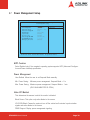
1
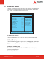
ETX
ETX-IM333
User’s Manual
ver. 1.1
Copyright 2005 ADLINK Technology Inc.
All Rights Reserved.
Manual Rev. 1.1: March 24, 2005
This document contains proprietary information protected by copyright laws. All rights are
reserved. No part of this manual may be reproduced by any mechanical, electronic, or other
means in any form without prior written permission of the manufacturer.
This document is provided for informational purposes only. The manufacturer makes no
representations or warranties with respect to the contents or use of this manual and specifically
disclaims any express or implied warranties of merchantability or fitness for any particular
purpose. The user will assume the entire risk of the use or the results of the use of this document. Further, the manufacturer reserves the right to revise this publication and make changes
to its contents at any time, without obligation to notify any person or entity of such revisions or
changes.
In no event will the manufacturer be liable for direct, indirect, special, incidental, or consequential damages arising out of the use or inability to use the product or documentation, even
if advised of the possibility of such damages.
Trademarks
PC is a registered trademark of International Business Machines Corporation. Intel is a registered trademark of Intel Corporation. AWARD is a registered trademark of Award Software
International, Inc. Other product names mentioned herein are used for identification purposes
only and may be trademarks and/or registered trademarks of their respective companies.
Page 2
ETX-IM333 User’s Manual
Revision History
Release
Date
Initials
Change
1.0
1.1
01/14/2005
03/23/2005
JC
HB
Initial release
Correct X3 and X4 pinouts
Add Speedstep note to BIOS CPU speed settings page 41
ETX-IM333 User’s Manual
Page 3
Contents
1
Introduction . . . . . . . . . . . . . . . . . . . . . . . . . . . . . . . . . . . . . . . . . . . . . . . . . 7
1.1
2
Description . . . . . . . . . . . . . . . . . . . . . . . . . . . . . . . . . . . . . . . . . . . . . . . . . . . . . 7
Specifications . . . . . . . . . . . . . . . . . . . . . . . . . . . . . . . . . . . . . . . . . . . . . . . 8
2.1
2.2
2.3
2.4
2.5
2.6
2.7
General . . . . . . . . . . . . . . . . . . . . . . . . . . . . . . . . . . . . . . . . . . . . . . . . . . . . . . . .
Display . . . . . . . . . . . . . . . . . . . . . . . . . . . . . . . . . . . . . . . . . . . . . . . . . . . . . . . .
TV-out (optional) . . . . . . . . . . . . . . . . . . . . . . . . . . . . . . . . . . . . . . . . . . . . . . . . .
Audio . . . . . . . . . . . . . . . . . . . . . . . . . . . . . . . . . . . . . . . . . . . . . . . . . . . . . . . . .
LAN . . . . . . . . . . . . . . . . . . . . . . . . . . . . . . . . . . . . . . . . . . . . . . . . . . . . . . . . . . .
Multi I/O . . . . . . . . . . . . . . . . . . . . . . . . . . . . . . . . . . . . . . . . . . . . . . . . . . . . . . . .
Mechanical and Environmental . . . . . . . . . . . . . . . . . . . . . . . . . . . . . . . . . . . . .
8
8
8
9
9
9
9
3
Function diagram . . . . . . . . . . . . . . . . . . . . . . . . . . . . . . . . . . . . . . . . . . . 10
4
Mechanical Dimensions . . . . . . . . . . . . . . . . . . . . . . . . . . . . . . . . . . . . . . 11
5
Watchdog Timer . . . . . . . . . . . . . . . . . . . . . . . . . . . . . . . . . . . . . . . . . . . . . 12
6
Connectors . . . . . . . . . . . . . . . . . . . . . . . . . . . . . . . . . . . . . . . . . . . . . . . . . 15
6.1
6.2
6.3
6.4
6.5
6.6
7
Connector Location . . . . . . . . . . . . . . . . . . . . . . . . . . . . . . . . . . . . . . . . . . . . .
Pin-Out Compatibillity . . . . . . . . . . . . . . . . . . . . . . . . . . . . . . . . . . . . . . . . . . . .
X1 Connector: PCI-bus, USB, and Audio . . . . . . . . . . . . . . . . . . . . . . . . . . . .
X2 Connector: ISA Bus . . . . . . . . . . . . . . . . . . . . . . . . . . . . . . . . . . . . . . . . . .
X3 Connector: CRT, LCD, Video, COM1/2, LPT1, IrDA, Mouse, Keyboard . .
X4 Connector: IDE1, IDE2, Ethernet, Miscellaneous . . . . . . . . . . . . . . . . . . .
15
15
16
17
18
19
System Resources . . . . . . . . . . . . . . . . . . . . . . . . . . . . . . . . . . . . . . . . . . . 20
7.1
7.2
7.3
7.4
7.5
Page 4
Interrupt Assignment . . . . . . . . . . . . . . . . . . . . . . . . . . . . . . . . . . . . . . . . . . . . .
PCI Bus Arbitration Assignment. . . . . . . . . . . . . . . . . . . . . . . . . . . . . . . . . . . . .
PCI Interrupt Routing . . . . . . . . . . . . . . . . . . . . . . . . . . . . . . . . . . . . . . . . . . . . .
Memory Map . . . . . . . . . . . . . . . . . . . . . . . . . . . . . . . . . . . . . . . . . . . . . . . . . .
Direct Memory Access Channels . . . . . . . . . . . . . . . . . . . . . . . . . . . . . . . . . . .
ETX-IM333 User’s Manual
20
21
21
21
21
7.6
7.7
8
I/O Address Map . . . . . . . . . . . . . . . . . . . . . . . . . . . . . . . . . . . . . . . . . . . . . . . 22
System Management Bus (I2C compatible) . . . . . . . . . . . . . . . . . . . . . . . . . . 22
Phoenix Award BIOS . . . . . . . . . . . . . . . . . . . . . . . . . . . . . . . . . . . . . . . . . 24
8.1
8.2
8.3
8.4
8.5
8.6
8.7
8.8
8.9
8.10
8.11
Description . . . . . . . . . . . . . . . . . . . . . . . . . . . . . . . . . . . . . . . . . . . . . . . . . . . .
Main Menu Setup Items . . . . . . . . . . . . . . . . . . . . . . . . . . . . . . . . . . . . . . . . . .
Standard CMOS Features . . . . . . . . . . . . . . . . . . . . . . . . . . . . . . . . . . . . . . . .
Advanced BIOS Features . . . . . . . . . . . . . . . . . . . . . . . . . . . . . . . . . . . . . . . . .
Advanced Chipset Features . . . . . . . . . . . . . . . . . . . . . . . . . . . . . . . . . . . . . . .
Integrated Peripherals . . . . . . . . . . . . . . . . . . . . . . . . . . . . . . . . . . . . . . . . . . .
Power Management Setup . . . . . . . . . . . . . . . . . . . . . . . . . . . . . . . . . . . . . . . .
PnP/PCI Configurations . . . . . . . . . . . . . . . . . . . . . . . . . . . . . . . . . . . . . . . . . .
PC Health Status . . . . . . . . . . . . . . . . . . . . . . . . . . . . . . . . . . . . . . . . . . . . . . . .
BIOS POST Messages . . . . . . . . . . . . . . . . . . . . . . . . . . . . . . . . . . . . . . . . . . .
BIOS POST Codes . . . . . . . . . . . . . . . . . . . . . . . . . . . . . . . . . . . . . . . . . . . . . .
24
24
26
29
32
35
39
42
44
45
47
Warranty Policy . . . . . . . . . . . . . . . . . . . . . . . . . . . . . . . . . . . . . . . . . . . . . 53
ETX-IM333 User’s Manual
Page 5
Page 6
ETX-IM333 User’s Manual
1 Introduction
1.1
Description
ETX-IM333 is an ETX compatible module specially designed to facilitate speedy development
of semi custom designs. ETX is an open standard that targets the market for embedded OEM
projects. An ETX core combined with a custom made carrier board represents a value solution
that allows OEM customers to get to the market fast. ETX Core modules are also known as
COM (Computer on module) or as SOM (System on Module). ETX-IM333 is fully compliant with
ETX component SBC™ Specification V2.6.
ETX-IM333 is based on the Intel’s embedded 855GME Northbridge
and ICH4 Southbridge. It supports Celeron® M and Pentium® M
(Banias/Dothan) CPU’s in the range of 600MHz to 1.7GHz. The CPU /
Chipset combination is ideal for applications that require high performance, reliability, and long product availability.
The Intel® 855GME Chipset graphics memory controller hub (GMCH-M) provides integrated
graphics (250MHz) capabilities and power saving features. The 855GME Northbridge incorporates a DDR memory controller and supports DDR333 in addition to DDR266/200 memory for
up to 1GB in a single 200-pin SODIMM socket. Graphic support for CRT and single/dual
channel LVDS is included. Optionally, the board can support TV 0ut (SDTV and HDTV).
The integrated EIDE controller supports both PIO and UDMA modes, USB ports v2.0, two
serial ports, one parallel port (SPP/ECP/EPP), one PS2 keyboard/mouse interface, AC97
audio interface, Fast Ethernet LAN controller, and power management functionality.
ETX-IM333 User’s Manual
Page 7
2 Specifications
2.1
General
f CPU: lntel® Pentium® M (Banias/Dothan type) or lntel® Celeron® M
supports soldered LV / ULV uFCBGA packages or uFCPGA socket
f Chipset: lntel® 855GME with 400 FSB and Intel® 82801DB I/O Control Hub 4
f Memory: one SODIMM socket for up to 1GB DDR 200/266/333
f L2 Cache: 512KB (Celeron-M), 1 MB (Pentium-M Banias), 2 MB (Pentium-M Dothan)
f Enhanced IDE: two ports and up to four ATAPI devices,
supports Ultra DMA transfer rates of up to 33 MB/sec
f BIOS: Phoenix AWARD PnP 4 Mb Flash with console redirection and CMOS EEPROM
backup. USB boot/legacy and PXE support
f Hardware Monitor: integrated in Winbond 83627HF
monitors supply voltages and CPU temperature
f Watchdog: integrated in Winbond 83627HF
software programmable 1-255 sec or 1-255 min, generates system reset
f Expansion: 32-bit PCI 2.2
2.2
Display
f Chipset: integrated Intel® 855GME Chipset graphics memory controller hub (GMCH-M)
supports Dual Independent Display on CRT and LVDS channel
f Memory: up to 32 MB UMA Video RAM
f CRT: up to QXGA 2048 x 1536
f Flat Panel: supports single/dual channel LVDS (2x12-bit)
for display resolutions up to 1600x1200
2.3
TV-out (optional)
f Chipset: Philips SAA-7104/05 Advanced Digital Video Encoder
f Output: PAL or NTSC legacy video output up to 1280 X 1024, HDTV supported
Page 8
ETX-IM333 User’s Manual
2.4
Audio
f Chipset: integrated in Intel® 82801DB Southbridge
f Audio Codec: VIA VT1616 AC97 ver. 2.0
2.5
LAN
f Chipset: ICH4 integrated Intel® 82562 compatible 32-bit PCI LAN controller
f Interface: 10/100 Mbps with Wake-on-LAN and Alert on LAN support
2.6
Multi I/O
f Serial: two high speed RS-232C ports (COM1/COM2)
f Parallel: SPP, EPP, and ECP mode
f FDD: not implemented
f IrDA: supports SIR IrDA 1.1 compliant
f USB: supports up to four ports ver 2.0 (ver 1.1 backward compatible)
f Keyboard & Mouse: one PS/2 keyboard and one PS/2 mouse
2.7
Mechanical and Environmental
f Power Requirement (+5V only): 18 Watt typical; (uFCBGA Pentium® M 1.1GHz with 512 MB
DDR333)
f Operating Temperature: 0 to 55°C (32 to 140°F)
f Relative Humidity: up to 90% @ 55°C
f ETX Board Dimensions: 95 mm x 114 mm (3.7" x 4.5")
f Weight: 87 grams
ETX-IM333 User’s Manual
Page 9
3 Function diagram
CPU
CPU
Intel
Intel
Ethernet
PHY
Ethernet
82562 PHY
82562
Northbridge
Northbridge
Intel 855GME
Intel® 855GME
AGP
VGA
SDRAM
DDR266
Memory
Controller
Philips
EEPROM
EEPROM
CMOS
CMOS
Backup
Backup
I2C
HUB
Interface
1.5
Southbridge
Southbridge
Intel ICH4
®
Intel® ICH4 PCI
EIDE
ATA
PCI Bus
Controller
Ethernet
MAC
VT1616
RTC
Audio
LPC
USB 2.0
VT1616
AC'97
Codec
AC'97
v2.0Codec
v2.0
Dual channel USB 2.0
BIOS
BIOS
Keyboard
X3
X3
If necessary
ISA bus to be
layed out on
Carrier
Digital
Video Out
LVDS
Philips
TV Out
Encoder
TV Out Encoder
SAA7104
(opt)
SAA7104 (opt)
SODIMM
SODIMM
Socket
Socket
®
LVDS
24-bit
CRT
DDR 266/333
DDR 266/333
X2
X2
ATA 33
X1
X1
X4
X4
Pentium® M
®
® M
Pentium
M
Celeron
®
SMT Celeron
uFCBGA2Mor
SMT uFCBGA2
socket
uFCPGA or
socket uFCPGA
Mouse
LPT1/FDD
COM1
Winbond
Winbond
LPC
Super I/O
header
LPC Super I/O
W83627HF
W83627HF
Watchdog
COM2
Page 10
ETX-IM333 User’s Manual
4 Mechanical Dimensions
X4
X2
X3
X1
ETX-IM333 User’s Manual
Page 11
5 Watchdog Timer
ETX-IM333 implements a watchdog timer embedded in the LPC
based Winbond 83627HF Super I/O controller.
The Watchdog timer consists of a one-second/minute resolution
down counter (in CRF6 of logical device 8 of 83627HF) and two
Watchdog control registers (CRF5 and CRF7 of logical device 8).
Once a value is set in the WDT, the timer begins to count down.
Any movement in the keyboard, mouse, or software re-set of the value will cause a reload of
the timer value. The Watchdog output is connected to "reset". When the system hangs up
without software re-trigger, the system will be reset.
The Watchdog timer that has a 1 second granularity up to 255 seconds or a 1 minute granularity up to 255 minutes. The keyboard and mouse will only reset WDT if Bit 7 and 6 of CRF7 is
set, that is values greater than C0h or 192 decimal.
To configure the registers, the following sequence should be followed :
f
1. Writing 87h to location 2Eh twice to enter into the extended function mode.
f
2. Configure the registers to set up WDT.
f
3. Writing 0AAh to location 2Eh to exit the extended function mode.
The example shown on the next page will reset the system after 15 seconds. Both keyboard
and mouse interrupts will reload WDT from CRF6.
Page 12
ETX-IM333 User’s Manual
begin :
;----------------------------------------------------;
Enter the extend function mode, interrupt double-write
;----------------------------------------------------mov
mov
out
out
mov
mov
out
mov
mov
out
dx,2eh
al,87h
dx,al
dx,al
dx,2eh
al,2bh ; CR2B,
bit4-> 0 = WDTO
; bit4-> 1 = GP24
dx,al
dx,2fh
al,0c0h
dx,al
mov
mov
out
mov
mov
out
dx,2eh
al,07h
dx,al
dx,2fh
al,08h
dx,al
mov
mov
out
mov
mov
out
dx,2eh
al,30h
dx,al
dx,2fh
al,01h
dx,al
mov
mov
out
mov
mov
out
dx,2eh
al,07h
dx,al
dx,2fh
al,08h
dx,al
mov
mov
out
mov
mov
out
dx,2eh
al,0f7h
dx,al
dx,2fh
al,0c0h
dx,al
ETX-IM333 User’s Manual
;device 8
;enable device 8
;device 8
;device 8,CRF7
Page 13
mov
mov
out
mov
mov
out
dx,2eh
al,07h
dx,al
dx,2fh
al,08h
dx,al
mov
mov
out
mov
mov
dx,2eh
al,0f5h
dx,al
dx,2fh
al,00h
out
dx,al
mov
mov
out
mov
mov
out
mov
mov
out
mov
mov
out
dx,2eh
al,07h
dx,al
dx,2fh
al,08h
dx,al
dx,2eh
al,0f6h
dx,al
dx,2fh
al,0fh
dx,al
;device 8
;device 8, CRF5
; bit3 -> 0 = second
; bit3 -> 1 = minute
;device 8
;device 8, CRF6
;-----------------------------------; Exit extend function mode
;-----------------------------------mov
mov
out
dx,2eh
al,0aah
dx,al
.exit
end
Page 14
ETX-IM333 User’s Manual
6 Connectors
6.1
Connector Location
- Ethernet
- IDE1 / IDE2
- Power Signals
- Speaker, Battery
- I2C & SMB bus
- ISA bus
X4
X2
ETX Core
Module
(top view)
X3
- VGA / LCD/ Video
- COM1 / COM2
- LPT1
- IrDA
- Mouse
- Keyboard
6.2
X1
- 32-bit PCI bus
- USB
- Audio
Pin-Out Compatibillity
All pin-outs on X1, X2, X3, and X4 of the ETX-IM333 comply with pin-out and signal description
used in the original : “ETX Specification ver 2.6”. This document contains a description of
pin-outs, signal descriptions, and mechanical characteristics of the ETX formfactor.
An additional document, “ETX Design Guide” gives a general introduction to carrier board
designs for ETX modules.
ETX-IM333 User’s Manual
Page 15
6.3
X1 Connector:
PCI-bus, USB, and Audio
1
Signals and Pinout
Page 16
99
Pin
Signal
Pin
Signal
Pin
Signal
Pin
Signal
1
3
5
7
9
11
13
15
17
19
21
23
25
27
29
31
33
35
37
39
41
43
45
47
49
GND
PCICLK3
GND
PCICLK1
REQ3#
GNT2#
REQ2#
REQ1#
GNT0#
5VCC
SERIRQ
AD0
AD1
AD4
AD6
CBE0#
AD8
GND
AD10
AD11
AD12
AD13
AD14
AD15
CBE1#
2
4
6
8
10
12
14
16
18
20
22
24
26
28
30
32
34
36
38
40
42
44
46
48
50
GND
PCICLK4
GND
PCICLK2
GNT3#
3V
GNT1#
3V
RSV
5VCC
REQ0#
3V
AD2
AD3
AD5
AD7
AD9
GND
AUXAL
MIC
AUXAR
ASVCC
SDNL
ASSGND
SNDR
51
53
55
57
59
61
63
65
67
69
71
73
75
77
79
81
83
85
87
89
91
93
95
97
99
5VCC
PAR
GPERR
PME#
LOCK#
TRDY#
IRDY#
FRAME#
GND
AD16
AD17
AD19
AD20
AD22
AD23
AD24
5VCC
AD25
AD28
AD27
AD30
PCIRST#
INTC#
INTA#
GND
52
54
56
58
60
62
64
66
68
70
72
74
76
78
80
82
84
86
88
90
92
94
96
98
100
5VCC
SERR#
RSV
USB2N
DEVSEL#
USB3N
STOP#
USB2P
GND
CBE2#
USB3P
AD18
USB0N
AD21
USB1N
CBE3#
5VCC
AD26
USB0P
AD29
USB1P
AD31
INTD#
INTB#
GND
ETX-IM333 User’s Manual
2
100
6.4
X2 Connector:
ISA Bus
1
Signals and Pinout
99
Pin
Signal
Pin
Signal
Pin
Signal
Pin
Signal
1
3
5
7
9
11
13
15
17
19
21
23
25
27
29
31
33
35
37
39
41
43
45
47
49
GND
NC
NC
NC
NC
NC
NC
NC
NC
NC
NC
NC
NC
NC
NC
NC
NC
GND
NC
NC
NC
NC
NC
NC
NC
2
4
6
8
10
12
14
16
18
20
22
24
26
28
30
32
34
36
38
40
42
44
46
48
50
GND
NC
NC
NC
NC
NC
NC
NC
NC
NC
NC
NC
NC
NC
NC
NC
NC
GND
NC
NC
NC
NC
NC
NC
NC
51
53
55
57
59
61
63
65
67
69
71
73
75
77
79
81
83
85
87
89
91
93
95
97
99
5VCC
NC
NC
NC
NC
NC
NC
NC
GND
NC
NC
NC
NC
NC
NC
NC
5VCC
NC
NC
NC
NC
NC
NC
NC
GND
52
54
56
58
60
62
64
66
68
70
72
74
76
78
80
82
84
86
88
90
92
94
96
98
100
5VCC
NC
NC
NC
NC
NC
NC
NC
GND
NC
NC
NC
NC
NC
NC
NC
5VCC
NC
NC
NC
NC
NC
NC
NC
GND
ETX-IM333 User’s Manual
2
100
Page 17
6.5
X3 Connector:
CRT, LCD, Video, COM1/2, LPT1,
IrDA, Mouse, Keyboard
1
Signals and Pinout
Page 18
99
Pin
Signal
Pin
Signal
Pin
Signal
Pin
Signal
1
3
5
7
9
11
13
15
17
19
21
23
25
27
29
31
33
35
37
39
41
43
45
47
49
GND
R
HSY
VSY
NC
LCD16
LCD17
GND
LCD13
LCD12
GND
LCD8
LCD9
GND
LCD4
LCD5
GND
LCD1
LCD0
5Vcc
NC
NC
NC
COMP
SYNC
2
4
6
8
10
12
14
16
18
20
22
24
26
28
30
32
34
36
38
40
42
44
46
48
50
GND
B
G
DDCK
DDDA
LCD18
LCD19
GND
LCD15
LCD14
GND
LCD11
LCD10
GND
LCD7
LCD6
GND
LCD3
LCD2
5Vcc
LTGO0
BLON#
DIGON
Y
C
51
53
55
57
59
61
63
65
67
69
71
73
75
77
79
81
83
85
87
89
91
93
95
97
99
LPT/FDD
5Vcc
STB#
RSV
IRRX
IRTX
RXD2
GND
RTS2#
DRT2#
DCD2#
DSR2#
CTS2#
TXD2
RI2
5Vcc
RXD1#
RTS1#
DRT1#
DCD1#
DSR1#
CTS1#
TXD1
RI#
GND
52
54
56
58
60
62
64
66
68
70
72
74
76
78
80
82
84
86
88
90
92
94
96
98
100
RSV
GND
AFD#
PD7
ERR#
PD6
INIT#
GND
PD5
SLIN#
PD4
PD3
PD2
PD1
PD0
5Vcc
PACK#
BUSY#
PE
SLCT#
MSCLK
MSDAT
KBCLK
KBDAT
GND
ETX-IM333 User’s Manual
2
100
6.6
X4 Connector:
IDE1, IDE2, Ethernet, Miscellaneous
1
Signals and Pinout
99
Pin
Signal
Pin
Signal
Pin
Signal
Pin
Signal
1
3
5
7
9
11
13
15
17
19
21
23
25
27
29
31
33
35
37
39
41
43
45
47
49
GND
5V_SB
PS_ON
PWRBTN#
KBINH
RSMRST#
NC
NC
5Vcc
OVCR#
EXTSMI#
SMBCLK
S_CS3#
S_CS1#
S_A2
S_A0
GND
PDIAG_S
S_A1
S_INTRQ
NC
S_AK#
S_RDY
S_IOR#
5Vcc
2
4
6
8
10
12
14
16
18
20
22
24
26
28
30
32
34
36
38
40
42
44
46
48
50
GND
PWGIN
SPEAKER
BATT
LILED
ACTLED
SPDLED
I2CLK
5Vcc
NC
I2DAT
SMBDATA
SMBALRT#
NC
P_CS3#
P_CS1#
GND
P_A2
P_A0
P_A1
NC
P_INTRQ
P_AK#
P_RDY
5Vcc
51
53
55
57
59
61
63
65
67
69
71
73
75
77
79
81
83
85
87
89
91
93
95
97
99
S_IOW#
S_DRQ
S_D15
S_D0
S_D14
S_D1
S_D13
GND
S_D2
S_D12
S_D3
S_D11
S_D4
S_D10
S_D5
5Vccz
S_D9
S_D6
S_D8
GPE2#
RXD#
RXD
TXD#
TXD
GND
52
54
56
58
60
62
64
66
68
70
72
74
76
78
80
82
84
86
88
90
92
94
96
98
100
P_IOR#
P_IOW#
P_DRQ
P_D15
P_D0
P_D14
P_D1
GND
P_D13
P_D2
P_D12
P_D3
P_D11
P_D4
P_D10
5Vcc
P_D5
P_D9
P_D6
CBLID_P#
P_D8
S_D7
P_D7
HDRST#
GND
ETX-IM333 User’s Manual
2
100
Page 19
7 System Resources
7.1
Interrupt Assignment
PCI and ISA interrupts supported by the Intel® FW82801DA South Bridge are as follows:
ISA IRQ
Edge/ Level
Polarity
Interrupt Source
Notes
NMI
IRQ0
IRQ1
IRQ2
IRQ3
IRQ4
IRQ5
IRQ6
IRQ7
IRQ8_L
IRQ9
IRQ10
IRQ11
IRQ12
IRQ13
IRQ14
IRQ15
Edge
Edge
Edge
Edge
Edge
Edge
Edge
Edge
Edge
Edge
Edge
Level
Level
Edge
Edge
Edge
Edge
High
High
High
High
High
High
Low
High
High
Low
Low
Low
Low
High
High
High
High
SERR_L asserted
Timer0
Keyboard
Cascade Interrupt from Slave Interrupt Controller
COM2
COM1
PCI PnP IRQ
(1)
(2)
(2)
(2)
LPT1
Real Time Clock
PCI PnP IRQ
PCI PnP IRQ
PCI PnP IRQ, USB
Mouse
FERR_L asserted
Primary IDE
Secondary IDE
(2)
(2)
(3)
(2)
(4)
(5)
Notes:
1f Internally generated by the FW82801DA.
2f Suggested. These interrupts are plug and play compatible and may be routed to any
available interrupt.
3f The USB interrupt is internally routed to the PIRQD# input of the FW82801DA.
4f This interrupt is routed to the IRQ14 input of the FW82801DA.
5f This interrupt is routed to the IRQ15 input of the FW82801DA.
Page 20
ETX-IM333 User’s Manual
7.2
PCI Bus Arbitration Assignment
PCI Bus Request
PCI Master(s)
IDSEL
Request 0
Request 1
Request 2
Request 3
Routed to ETX connector X1
Routed to ETX connector X1
Routed to ETX connector X1
Routed to ETX connector X1
*
*
*
*
Note: IDSEL routing depends on the design of the carrier board.
7.3
7.4
7.5
PCI Interrupt Routing
Device
Net PIRQ0_L
Net PIRQ1_L
Net PIRQ2_L
Net PIRQ3_L
ETX Connector X1
PIRQA#
PIRQB#
PIRQC#
PIRQD#
Memory Map
Address
Size
Description
00000000~0009FFFF
000A0000~000BFFFF
000C0000~000DFFFF
000E0000~000EFFFF
000F0000~000FFFFF
00100000~DRAM Top
DRAM Top ~FFFRFFFF
FFFEFFFF ~ FFFFFFFF
640K
128K
128K
64K
64K
----64K
DOS Application Area
Video Buffer Area
Expansion Area
Extended System BIOS Area
System BIOS Area
System memory area
Bus area
Initialization area
Direct Memory Access Channels
DMA#
Available
0
1
2
3
4
5
6
7
Yes
Yes
Yes
Yes
No
Yes
Yes
Yes
ETX-IM333 User’s Manual
Description
Unavailable if Sound Blaster is enabled with default configuration
because FDC not impleneted
Unavailable when LPT is in ECP mode
Used for Cascade
Page 21
7.6
7.7
I/O Address Map
Address
Size
Description
0000 - 001F
0020 - 002D
0040 - 005F
0060 - 006F
60h
61h
64h
0070 - 0077
0078 - 007F
0080
0081 - 008F
0090 - 0091
0092
0093 - 009F
00A0 - 00BF
00C0 - 00DF
00E0 - 00FF
0100 - 0CF7
0CF8 -0CFB
0CFC - 0CFF
0D00 - FFFF
32 bytes
14 bytes
32 bytes
32 bytes
1 byte
1 byte
1 byte
8 bytes
8 bytes
1 byte
16 bytes
2 bytes
1 byte
13 bytes
32 bytes
32 bytes
32 bytes
Master DMA controller
Master Interrupt Controller
Timer/Counter
Keyboard Controller / NMI Controller
KBC data
Misc function and Speaker control
KBC command / status
RTC/CMOS/NMI Controller
Available for system use
Reserved (Debug port)
DMA page registers
Available for system use
System Control
Available for system use
Slave Interrupt Controller
Slave DMA Controller
Available for system use
Available for system use
PCI configuration address
PCI configuration data
Available for system use
4 bytes
4 bytes
System Management Bus (I2C compatible)
Internally the SMB bus and I2C bus are one and the same. The ICH4 Southbridge support
SMBDAT and SMBCLK lines that are I2C compatible.
The X4 connector has pinouts for both I2C and SMB bus. Both are connected to the same
internal bus: the SMB bus. It is advisable to always connect external I2C devices to the I2C
pins and SMB devices to the SMB pins to stay compatible with other modules that might
support two internal busses (separate I2C and SMB bus)
Page 22
Address
Function
Device
A0h
AEh
D2h
Identification Info
CMOS setting backup
Timing
SODIMM0 EEPROM
EEPROM
Clock generator
ETX-IM333 User’s Manual
ETX-IM333 User’s Manual
Page 23
8 Phoenix Award BIOS
8.1
Description
The module has a Phoenix Award PCI/ISA BIOS ver 6.0 for the system configuration. The
Award BIOS setup program is designed to provide the maximum flexibility in configuring the
system by offering various options which could be selected for end-user requirements. This
chapter is written to assist you in the proper usage of these features.
To access the Phoenix AWARD PCI/ISA BIOS Setup program,
press <Del> key.
The Main Menu will then be displayed.
Phoenix - AwardBIOS CMOS SETUP UTILITY
Standard CMOS Features
Frequency/Voltage Control
Advanced BIOS Features
Load Fail-Safe Defaults
Advanced Chipset Features
Load Optimized Defaults
Integrated Peripherals
Set Supervisor Password
Power Management Setup
Set User Password
PnP/PCI Configurations
Save & Exit Setup
PC Health Status
Exit Without Saving
Esc: Quit
F9 : Menu in BIOS
F10: Save and Exit
↑ ↓ → ←
: Select Item
Time, Date, Hard Disk Type...
8.2
Main Menu Setup Items
The main menu includes the following main setup categories. Recall that some systems may
not include all entries.
Standard CMOS Features (see paragraph 9.3)
Use this menu for basic system configuration.
Advanced BIOS Features (see paragraph 9.4)
Use this menu to set the Advanced Features available on your system.
Page 24
ETX-IM333 User’s Manual
Advanced Chipset Features (see paragraph 9.5)
Change values in the chipset registers and optimize your system's performance.
Integrated Peripherals (see paragraph 9.6)
Use this menu to specify your settings for integrated peripherals.
Power Management Setup (see paragraph 9.7)
Use this menu to specify your settings for power management.
PnP / PCI Configuration (see paragraph 9.8)
This entry appears if your system supports PnP / PCI.
PC Health Status (see paragraph 9.9)
Use this menu to monitor CPU and system temperatures.
Frequency/Voltage Control
Use this menu to specify your settings for frequency/voltage control.
Load Fail-Safe Defaults
Loads the BIOS default values for the minimal/stable performance for your system to operate.
Load Optimized Defaults
Loads the BIOS default values that are factory settings for optimal system performance.
Supervisor/User Password
Use this menu to set User and Supervisor Passwords.
Save & Exit Setup
Save CMOS value changes to CMOS and exit setup.
Exit Without Saving
Abandon all CMOS value changes and exit setup.
ETX-IM333 User’s Manual
Page 25
8.3
Standard CMOS Features
The main menu includes the following main setup categories. Recall that some systems may
not include all entries.
Phoenix - AwardBIOS CMOS SETUP UTILITY
Standard CMOS Features
Date: (mm:dd:yy)
Time: (hh:mm:ss)
Fri, Nov 07 2003
18:20:31
IDE
IDE
IDE
IDE
[None]
[None]
[None]
[None]
Primary Master
Primary Slave
Secondary Master
Secondary Slave
Item Help
Change the day, month,
year and century
Drive A
[None]
Video
Halt On
[EGA/VGA]
[All , but Keyboard]
Base Memory
Extended Memory
Total Memory
640K
252928K
253952K
↑ ↓ → ← :Move Enter:Select +/-/PU/PD:Value F10:Save ESC:Exit F1:General Help
F5:Previous Values
F6:Fail-Safe Defaults
F7:Optimized Defaults
Date
The BIOS determines the day of the week from the other date information; this field is for
information only.
Time
The time format is based on the 24-hour military-time clock. For example, 1 p.m. is 13:00:00.
Press the « or ( key to move to the desired field Press the PgUp or PgDn key to increment
the setting, or type the desired value into the field.
IDE Primary and Secondary Master/Slave Items
This selection brings up a configuration menu of the designated Drive (see next page)
Page 26
ETX-IM333 User’s Manual
Drive A
The ETX-IM333 can support one single FDD drive. Because FDD and LPT1 share the same
pins on the X3 connector, only one of them can be used at a time. LPT1 or FDD can be
enabled in the following BIOS menu:
fIntegrated Peripherals fSuper I/O Device fLPT1 Setting / FDD
This menu allows setup of LPT1 resources or disabling of LPT1 and setting the mode to FDD.
After enabling the FDD, select the correct specifications for the diskette drive:
None:
No diskette drive installed
360K:
5.25 inch PC-type standard drive
1.2M:
5.25 inch AT-type high-density drive
720K:
3.5 inch double-sided drive
1.44M:
3.5 inch double-sided drive
2.88M:
3.5 inch double-sided driveIDE Primary and Secondary Master/Slave Items
Video
Select the type of primary video subsystem in your computer. The BIOS usually detects the
correct video type automatically. The BIOS supports a secondary video subsystem, but this is
not selected in Setup.
Halt On
During the Power On Self Test (POST), the computer stops if the BIOS detects a hardware
error. The BIOS can be instructed to ignore certain errors during POST and continue the bootup process. The options are as follows:
No errors:
POST does not stop for any errors.
All errors:
POST stops for any non-fatal error and will prompt the user to take any
corrective measures.
All, But Keyboard:
POST does not stop for a keyboard error, but stops for all other errors
All, But Diskette:
POST does not stop for diskette drive errors, but stops for all other
errors
All, But Disk/Key:
POST does not stop for a keyboard or disk errors, but stops for all other
errors
ETX-IM333 User’s Manual
Page 27
IDE Primary and Secondary Master/Slave Items
Phoenix - AwardBIOS CMOS SETUP UTILITY
IDE Primary Master
IDE HDD Auto-Detection
Press Enter
IDE Primary Master
Access Mode
Capacity
[Auto]
[Auto]
0 MB
Cylinder
Head
Precomp
Landing Zone
Item Help
Menu Level
To auto-detect the
HDD’s size, head .. on
this channel
0
0
0
0
↑ ↓ → ← :Move Enter:Select +/-/PU/PD:Value F10:Save ESC:Exit F1:General Help
F5:Previous Values
F6:Fail-Safe Defaults
F7:Optimized Defaults
IDE HDD Auto-detection
Press Enter
Press Enter to auto-detect the HDD on
this channel. If detection is successful, it fills the remaining fields on this
menu.
IDE Primary Master
None/Auto/Manual
Selecting 'manual' allows the user to set
the remaining fields on this screen.
Selects the type of fixed disk. "User
Type" will let you select the number of
cylinders, heads, etc. Note:
PRECOMP=65535 means NONE.
Capacity
Auto Display disk size
Disk drive capacity (Approximated).
Note that this size is usually slightly
greater than the size of a formatted
disk given by a disk checking program.
Access Mode
CHS/LBA/Large/Auto
Choose the access mode for this hard
disk
The following options are selectable only if the 'IDE Primary Master' item is set to 'Manual'
Page 28
Cylinder
Min = 0 Max = 65535
Set the number of cylinders for this
hard disk.
Head
Min = 0 Max = 255
Set the number of read/write heads
Precomp
Min = 0 Max = 65535
**** Warning: Setting a value of 65535
means no hard disk
Landing zone
Min = 0 Max = 65535
****
Sector
Min = 0 Max = 255
Number of sectors per track
ETX-IM333 User’s Manual
8.4
Advanced BIOS Features
This section allows the user to configure the system for basic operation. The following features
can be selected here: system default speed, boot-up sequence, keyboard operation, shadowing, security, and CPU Internal Cache/CPU External Cache.
Phoenix - AwardBIOS CMOS Setup Utility
Advanced BIOS Features
CPU L1 & L2 Cache
CPU L3 Cache
Quick Power On Self Test
First Boot device
Second Boot device
Third Boot device
Boot Other device
Boot Up NumLock Status
Gate A20 Option
Security Option
Console Redirection
x Baud Rate
Agent Connect via
Agent wait time(sec)
Agent aftr boot
Summary Screen Show
[Enabled]
[Enabled]
[Disabled]
[USB-FDD]
[HDD-0]
[CDROM]
[Disabled]
[Off]
[Normal]
[Setup]
[Setup]
115200
[NULL]
[3]
[Enabled]
[Disabled]
Item Help
Menu Level
Allows you to choose the
VIRUS warning feature
for IDE Hard Disk boot
sector protection. If
this function is enabled
and someone attempt to
write data into this
area, BIOS will show a
warning message on
screen and alarm beep
↑ ↓ → ← :Move Enter:Select +/-/PU/PD:Value F10:Save ESC:Exit F1:General Help
F5:Previous Values
F6:Fail-Safe Defaults
F7:Optimized Defaults
CPU L2 Cache ECC Checking
This function enables/disables CPU L2 Cache ECC checking. Options: Enabled, Disabled.
Quick Power On Self Test
This category speeds up the Power On Self Test (POST). If enabled, BIOS will shorten or skip
some check items during POST. Options: Enabled: enables quick POST. Disabled: normal
POST.
First/Second/Third Boot Device
Pressing Enter brings up the Boot Device Menu. The BIOS attempts to load the operating
system from the selected device.
See menu for possible options
ETX-IM333 User’s Manual
Page 29
Boot Other Device
When enabled, the BIOS will try to boot from second or
third option if booting from first device fails. When disabled the BIOS will not use the alternative devices
First Boot Device
LS120
HDD-0
SCSI
CDROM
HDD-1
HDD-2
HDD-3
ZIP100
USB-FDD
USB-ZIP
USB-CDROM
USB-HDD
LAN
Disabled
Boot Up NumLock Status
Select power on state for NumLock. Options: On/Off
Gate A20 Option
Select if chipset or keyboard controller should control GateA20.
Normal: A pin in the keyboard controller controls GateA20
Fast: Lets chipset control GateA20
....
....
....
....
....
....
....
....
....
....
....
....
....
....
[
[
[
[
[
[
[
[
[
[
[
[
[
[
]
]
]
]
]
]
]
]
]
]
]
]
]
]
↑ ↓ → ← :Move Enter:Accept ESC:Abort
Typematic Rate Setting
Key strokes repeat at a rate determined by the keyboard
controller. When enabled, the typematic rate and
typematic delay can be selected. Options: Enabled/Disabled.
Typematic Rate (Chars/Sec)
Sets the number of times per second to repeat a key stroke when holding down the key.
Options: 6, 8, 10, 12, 15, 20, 24, and 30.
Typematic Delay (Msec)
Sets the delay time after the key is held down before it begins to repeat the keystroke. Options: 250, 500, 750, and 1000.
Security Option
Select whether the password is required every time the system boots or only when you enter
setup. Chioces :
System: The system will not boot and access to Setup will be denied if an incorrect password
is entered at the prompt.
Setup : The system will boot, but access to Setup will be denied if an incorrect password is
not entered at the prompt.
Page 30
ETX-IM333 User’s Manual
To disable security, select PASSWORD SETTING in Main Menu. The user will then be
prompted to enter the password. Do not type anything and press <Enter> to disable security.
Once security is disabled, the system will boot and Setup can be entered freely.
OS Select For DRAM > 64MB
Select the operating system that is running with greater than 64MB of RAM on the system.
Options: Non-OS2, OS2.
Video BIOS Shadow
Enables copying of Video BIOS to shadow RAM. Improves performance.
Summary Screen Show
Suppress the summary screen. Options: Enable, Disable
ETX-IM333 User’s Manual
Page 31
8.5
Advanced Chipset Features
Phoenix - AwardBIOS CMOS Setup Utility
Advanced Chipset Features
DRAM Data Integrity Mode
MGM Core Frequency
System BIOS Cacheable
Video BIOS Cacheable
Delayed Transaction
Delay Prior to Thermal
AGP Aperture Size (MB)
BIOS Write Protection
[non ECC]
[Auto Max 266 Mhz]
[Disabled]
[Disabled]
[Enabled]
[16 Min]
[64]
[Disabled]
** On Chip VGA Settings **
Onchip VGA
Onchip Framebuffer size
Boot Display
LVDS Panel Type
[Enabled]
[32MB]
[CRT]
[640x480]
Item Help
Menu Level
↑ ↓ → ← :Move Enter:Select +/-/PU/PD:Value F10:Save ESC:Exit F1:General Help
F5:Previous Values
F6:Fail-Safe Defaults
F7:Optimized Defaults
DRAM Data Integrity Mode
ECC, which stands for Error Checking and Correction, enables the memory controller to detect
and correct single-bit soft memory errors. The memory controller will also be able to detect
double-bit errors though it will not be able to correct them. This provides increased data
integrity and system stability. However, this feature can only be enabled if you are using
special ECC memory modules.
Display may flicker when integrated graphics and ECC support are enabled !
Memory with ECC enabled requires more system memory resources. This will cause the
integrated graphics engine to have less memory bandwidth for access to the graphics frame
buffer. Display flicker and flashing may occur when ECC is enabled under high-resolution
graphics modes.
MGM Core Frequency
This field is to select the FSB Speed / Memory Speed / GFX Low / GFX high core frequency.
Default is Automax Max 266.
System BIOS Cacheable
Selecting Enabled allows caching of the system BIOS ROM at F0000h-FFFFFh, resulting in
better system performance. However, if any program writes to this memory area, a system
error may result.
Page 32
ETX-IM333 User’s Manual
Video RAM Cacheable
Select Enabled allows caching of the video RAM, resulting in better system performance.
However, if any program writes to this memory area, a system error may result.
Options: Enabled, Disabled, Fast R-W Turn Around.
Delayed Transaction
The chipset has an embedded 32-bit posted write buffer to support delay transactions cycles.
Select Enabled to support compliance with PCI specification version 2.1.
Delay Prior to Thermal
When the Thermal Monitor is in automatic mode and the thermal sensor detects that the processor has reached its maximum safe operating temperature, it will activate the TCC. The TCC
will then modulate the clock cycles by inserting null cycles, typically at a rate of 50-70% of the
total number of clock cycles. This results in the processor "resting" 50-70% of the time.
As the die temperature drops, the TCC will gradually reduce the number of null cycles until no
more is required to keep the die temperature below the safe point. The thermal sensor then
turns the TCC off. This mechanism allows the processor to dynamically adjust its duty cycles to
ensure its die temperature remains within safe limits.
The Delay Prior To Thermal BIOS feature controls the activation of the Thermal Monitor's
automatic mode. It allows the user to determine when the CPU's Thermal Monitor should be
activated in automatic mode after the system boots. For example, with the default value of 16
minutes, the BIOS activates the Thermal Monitor in automatic mode 16 minutes after the system
starts booting up.
Generally, the Thermal Monitor should not be activated immediately on booting as the processor will be under a heavy load during the booting process. This causes a sharp rise in die
temperature from its cold state. Because it takes time for the thermal output to radiate from the
die to the heat sink, the thermal sensor will register the sudden spike in die temperature and
prematurely activate the TCC. This unnecessarily reduces the processor's performance during
the booting up process.
Therefore, to ensure optimal booting performance, the activation of the Thermal Monitor must
be delayed for a set period of time.
It is recommended that this BIOS feature is set to the lowest value (in minutes) that exceeds
the time it takes to fully boot up your computer. For example, if it takes 5 minutes to fully boot
up your system, you should select 8 minutes.
You should not select a delay value that is unnecessarily long. Without the Thermal Monitor,
the processor may heat up to a critical temperature (approximately 135°C), at which point the
thermal sensor shuts down the processor by removing the core voltage within 0.5 seconds.
ETX-IM333 User’s Manual
Page 33
AGP Aperture Size (MB)
Select the size of Accelerated Graphics Port (AGP) aperture. The aperture is a portion of the
PCI memory address range dedicated for graphics memory address space. Host cycles that
hit the aperture range are forwarded to the AGP without any translation. Default is 64 MB.
Options: 4M, 8M, 16M, 32M, 65M, 128M, 256M.
BIOS Write Protection
This is a security feature that when enabled prohibits the user to Flash the BIOS. The default
setting is Disabled.
Onchip VGA
Can enable or disable the intgrated VGA core. The default setting is Enabled.
Onchip Framebuffer size
The selection lets you configure how much system memory you want to allocate to the integrated GPU. The amount you allocate to the GPU is deducted from the amount of system
memory available to your operating system and programs.
Do not assign more memory than absolutely required by the current VGA mode.
For example a resolution of 1600x1200 and colour depth of 32-bit,
amounts to 1600 x 1200 x 32-bits = 61,440,000 bits or 7.68MB.
Set to 8MB in this example.
Display Feature
This item allows the user to configure the type of external display used.
Options: CRT, LVDS (displays cannot be used concurrently)
LVDS Panel Type
When LVDS is selected in “Display Feature”, tthe flat panel resolution can be selected.
Options: 640x480 ,800x600, 1024x768, and 1280x1024.
Page 34
ETX-IM333 User’s Manual
8.6
Integrated Peripherals
Phoenix - AwardBIOS CMOS Setup Utility
Advanced Chipset Features
OnChip IDE Device
Onboar Device
SuperIO Device
Onboard LAN Boot ROM
[Press Enter]
[Press Enter]
[Disabled]
[Disabled]
Item Help
Menu Level
↑ ↓ → ← :Move Enter:Select +/-/PU/PD:Value F10:Save ESC:Exit F1:General Help
F5:Previous Values
F6:Fail-Safe Defaults
F7:Optimized Defaults
OnChip IDE Device (submenu)
Phoenix - AwardBIOS CMOS Setup Utility
VIA OnChip IDE Device
OnChip Primary PCI IDE
IDE Primary Master PIO
IDE Primary Slave PIO
IDE Primary Master UDMA
IDE Primary Slave UDMA
OnChip Secondary PCI IDE
IDE Secondary Master PIO
IDE Secondary Slave PIO
IDE Secondary Master UDMA
IDE Secondary Slave UDMA
[Enabled]
[Auto]
[Auto]
[Auto]
[Auto]
[Enabled]
[Auto]
[Auto]
[Auto]
[Auto]
IDE HDD Block Mode
[Disabled]
Item Help
Menu Level
↑ ↓ → ← :Move Enter:Select +/-/PU/PD:Value F10:Save ESC:Exit F1:General Help
F5:Previous Values
F6:Fail-Safe Defaults
F7:Optimized Defaults
OnChip Primary/Secondary PCI IDE
The chipset contains a PCI IDE interface with support for two IDE channels. Select Enabled to
activate the primary/secondary IDE interface. Select Disabled to deactivate these interfaces.
Primary & Secondary Master/Slave PIO
The four IDE PIO (Programmed Input/Output) fields allows the user to set a PIO mode (0-4) for
each of the four IDE devices that the onboard IDE interface supports. Modes 0 through 4
provide successively increased performance. In Auto mode, the system automatically determines the best mode for each device. Options: Auto, Mode 0, Mode 1, Mode 2, Mode 3,
Mode 4.
ETX-IM333 User’s Manual
Page 35
IDE Primary & Secondary Master/Slave UDMA
Ultra DMA implementation is possible only if your IDE hard drive supports it and the operating
environment includes a DMA driver. If your hard drive and your system software both support
Ultra DMA, select Auto to enable BIOS support.
IDE HDD Block Mode
This feature enhances disk performance by allowing multi-sector data transfers and eliminates
the interrupt handling time for each sector.
OnChip PCI Device (submenu)
Phoenix - AwardBIOS CMOS Setup Utility
VIA OnChip IDE Device
USB Controller
USB 2.0 Controller
USB Keyboard Support
AC97 Audio
Init Display First
[Enabled]
[Enabled]
[Enabled]
[Enabled]
[PCI Slot]
Item Help
Menu Level
↑ ↓ → ← :Move Enter:Select +/-/PU/PD:Value F10:Save ESC:Exit F1:General Help
F5:Previous Values
F6:Fail-Safe Defaults
F7:Optimized Defaults
USB Controller
This should be enabled to use the internal USB function. Enabling only results in USB 1.1
functionallity. To also obtain USB 2.0 functionallity the “USB 2.0 Controller” setting will also have
to be enabled. Options: Enabled, Disabled.
USB 2.0 Controller
This enables USB 2.0 support on the USB controller. Options: Enabled, Disabled.
USB Keyboard Support
Select Enabled if your system contains a Universal Serial Bus (USB) controller and you have a
USB keyboard. Options: Enabled, Disabled.
AC ‘97 Audio
This item allows you to control the onboard AC 97 audio. Options: Enable, Disabled.
Init Display First
This BIOS feature allows you to select whether to boot the system using the embedded AGP
graphics core or a possible PCI graphics card.
Page 36
ETX-IM333 User’s Manual
Super I/O Device
Phoenix - AwardBIOS CMOS Setup Utility
SuperIO Device
Onboard Serial Port 1
Onboard Serial Port 2
UART Mode Select
RxD, TxD Active
IR Transmission Delay
UR2 Duplex mode
Use IR Pins
Onboard Parellel Port
Parellel Port Mode
EPP Mode Select
ECP Mode Use DMA
[3F8/IRQ4]
[2F8/IRQ3]
[Normal]
[Hi/Lo]
[Enabled]
[Half]
[IR-Rx2Tx2]
[378/IRQ7]
[ECP+EPP]
[EPP1.9]
[3]
Item Help
Menu Level
↑ ↓ → ← :Move Enter:Select +/-/PU/PD:Value F10:Save ESC:Exit F1:General Help
F5:Previous Values
F6:Fail-Safe Defaults
F7:Optimized Defaults
Onboard Serial Port 1/2
Select address and interrupt for the serial ports.
UART Mode Select
The serial port 2 on your system offers a varierty of infrared modes. There are two different IR
(Infra-Red) modes - IrDA and ASK IR. Select the IR mode that is supported by your external IR
device. Choosing the wrong IR mode will prevent your computer from communicating with the
external IR device.
RxD, TxD Active
This BIOS feature allows you to set the infra-red reception (RxD) and transmission (TxD)
polarity.
IR Transmission Delay
When UART Mode is selected in IrDA or ASKIR mode, it allows the user to enable / disable IR
Transmission Delay.
UR2 Duplex Mode
This options controls the operating mode between receiving and transmitting of IrDA or ASKIR.
The operating mode will be synchronous bi-directional transmission and reception when Full
mode is selected. The operating mode will be asynchronous bi-directional transmission and
reception when Half mode is selected. Options: Half; Full
ETX-IM333 User’s Manual
Page 37
LPT1 Setting / FDD
This setting allows the user to assign resources to LPT1 or disable the function and allow using
an FDD drive. Since share LPT1 and FDD share the same pins on the X3 connector, only one
of them can be used at a time.
EPP Mode Select
There are two versions of the EPP transfer protocol - EPP 1.7 and EPP 1.9. This BIOS feature
allows the user to select the version of EPP that the parallel port should use.
Generally, EPP 1.9 is the preferred setting because it supports the newer EPP 1.9 devices
and most EPP 1.7 devices, while offering other advantages such as support for longer cables.
However, because certain EPP 1.7 devices cannot work properly with an EPP 1.9 port, this
BIOS feature was implemented to allow the user to set the EPP mode to EPP 1.7 when this
occurs.
Therefore, it is recommended that you sets this BIOS feature to EPP 1.9. However, if there are
problems connecting to the parallel port devices, switch to EPP 1.7.
ECP Mode Use DMA
This BIOS feature determines which DMA channel the parallel port should use when it is in ECP
mode. The ECP mode uses the DMA protocol to achieve data transfer rates of up to 2.5 Mbits/
s and provides symmetric bidirectional communications. For all this, it requires the use of a
DMA channel.
Page 38
ETX-IM333 User’s Manual
8.7
Power Management Setup
Phoenix - AwardBIOS CMOS Setup Utility
Power Management Setup
ACPI function
Power Management
Video Off Option
Video Off In Suspend
Suspend Type
Suspend Mode
HDD Power Down
Soft-off by PWR-BTTN
CPU THRM-Throttling
Wake-Up by PCI Card
[Enabled]
[User Define]
[Suspend -> Off]
[Yes]
[Stop Grant]
[Disable]
[Disable]
[Instant-Off]
[ 50.00%]
[Enabled]
Item Help
Menu Level
↑ ↓ → ← :Move Enter:Select +/-/PU/PD:Value F10:Save ESC:Exit F1:General Help
F5:Previous Values
F6:Fail-SAfe Defaults
F7:Optimized Defaults
ACPI Function
Select Enabled only if the computer's operating system supports ACPI (Advanced Configuration and Power Interface) specification.
Power Management
User Defined Allows the user to set Suspend Mode manually.
Min. Power Saving:
Minimum power management. Suspend Mode = 1 hr
Max. Power Saving: Maximum power management. Suspend Mode = 1 min.
(ONLY AVAILABLE FOR SL CPU's )
Video Off Method
This determines the manner in which the monitor is blanked.
Blank Screen: This option only writes blanks to the screen.
V/H SYNC+Blank: Causes the system to turn off the vertical and horizontal synchronization
signals and writes blanks to the screen.
DPMS Support: Display power management signaling.
ETX-IM333 User’s Manual
Page 39
Video Off in Suspend
When enabled, the video is turned off in suspend mode.
Suspend Mode
Select the Suspend Type. Options: PWRON Suspend, Stop Grant.
Suspend Type
When enabled and after the set time of system inactivity, all devices except CPU are shut off.
HDD Power Down
After the selected period of drive inactivity, the hard disk drive powers down while all other
devices remain active.
Soft-Off By PWR-BTTN
The field defines the power-off mode when using an ATX power supply. The Instant-Off mode
means the system will be powered off immediately when pressing the power button. In the
Delay 4 Sec mode, the system powers off when the power button is held down for more than
four seconds or places the system in a very low-power-usage state, with only enough circuitry
receiving power to detect power button activity or resume by ring activity when the power
button is held down for less than four seconds. The default is 'Instant-Off'.
State After Power Failure
On:
After a power failure, the system will automatically reboot as soon as power is re-stored.
Off:
After a power failure, the system will not reboot when power is restored. The system
needs to be turned on again manually.
Auto: After a power failure, the system will automatically reboot as soon as power is restored
if the PC was turned on when the power failed. If the PC was already turned off when the
power failed, the system needs to be turned on again manually.
CPU THRM-Throttling
Thermal Throttling, if enabled (default), is a safety feature against overheating that throttles a
processor back as it reaches its maximum operating temperature. Throttling does not change
the processor speed but instead reduces the number of available processing cycles, thereby
reducing the heat dissipation of the CPU. This cools down the CPU. Once the CPU has once
again reached a safe operating temperature, thermal throttling is automatically disabled, and
normal full speed processing resumes.
Options: Disabled, 87.5%, 75.0%, 62.5%, 50.0%, 37.5%, 25.0%, 12.5%
Page 40
ETX-IM333 User’s Manual
Wake-Up by PCI Card
This field should be set to Enabled only if your PCI card (e.g. LAN or modem card) uses the
PCI PME (Power Management Event) signal to remotely wake up the system. Accessing the
PCI card will cause the system to wake up. Refer to the card’s documentation for more information. If set to Disabled, the system will not wake up if the PCI card accessed.
Set CPU Speed/Voltage
This setting is only available for Pentium® M 1.6, 1.8, and 2.0 GHz CPUs
(both soldered and socket types).
To reduce overall power consumption or set a hard limit for thermal reasons, this BIOS setting
lets you lower the CPU Speed/Voltage. The OS itself cannot override settings in the BIOS, but
some Speedstep related software can please read below.
Although the BIOS supports all Pentium® and Celeron® M CPU’s, CPU Speed/Voltage switching is only supported for the Pentium® CPUs shown in the table below. Upon bootup, the
BIOS auto-detects the CPU type and speed and inserts the correct Speed/Voltage table into
the BIOS selection menu.
The default Speed/Voltage settings are shown in red bold. These values are used when
either “Load Failsafe Defaults” or “Load Optimized Defaults” are applied. Higher Speed/
Voltage settings must be set manually.
Banias type
1.6 GHz
Dothan Type
1.8 GHz
1.60GHz/1.484V
1.40GHz/1.420V
1.20GHz/1.276V *
1.00GHz/1.164V
800MHz/1.036V
600MHz/0.956V
1.80GHz/1.324V
1.60GHz/1.276V
1.40GHz/1.212V *
1.20GHz/1.164V
1.00GHz/1.100V
800MHz/1.052V
600MHz/0.988V
*
2.0 GHz
2.00GHz/1.324V
1.80GHz/1.276V
1.60GHz/1.228V
1.40GHz/1.180V *
1.20GHz/1.132V
1.00GHz/1.084V
800MHz/1.036V
600MHz/0.988V
Recommended max. speed/voltage when using heatspreader. These values are used when either
“Load Failsafe Defaults” or “Load Optimized Defaults” are applied.
WARNING
When certain operating systems are installed, such as Windows XP with Service Pack 2, the
above BIOS settings may be automatically overridden by native support for dynamic voltage
and frequency switching. This means that the CPU may be switched to a higher frequency and
voltage than is specified by the BIOS.
ETX-IM333 User’s Manual
Page 41
8.8
PnP/PCI Configurations
Phoenix - AwardBIOS CMOS Setup Utility
Power Management Setup
Reset Configuration Data [Disabled]
Resource Controlled By
x IRQ Resources
[Auto(ESCD)]
Press Enter
Item Help
Menu Level
Default is Disabled.
Select Enabled to
Reset Extended System
Configuration Data (ESCD)
when you Exit Setup if you
have installed a new
add-on and the system
reconfiguration has
caused such as serious
conflict that the OS
cannot boot
↑ ↓ → ← :Move Enter:Select +/-/PU/PD:Value F10:Save ESC:Exit F1:General Help
F5:Previous Values
F6:Fail-SAfe Defaults
F7:Optimized Defaults
This section describes the configuring of the PCI bus system. PCI, or Personal Computer
Interconnect, is a system which allows I/O devices to operate at speeds nearing the speed the
CPU itself uses when communicating with its own special components.
Reset Configuration Data
Normally, this field is left Disabled. Select Enabled to reset ESCD (Extended System Configuration Date) upon exiting Setup if a new add-on has been installed and the system reconfiguration
has caused such a serious conflict that the operating system cannot boot.
Resource Controlled By
The Award Plug and Play BIOS can automatically configure all the boot and Plug-and-Play
compatible devices. If Auto is selected, all interrupt requests (IRQ) and DMA assignment fields
disappear, as the BIOS automatically assigns them.
Page 42
ETX-IM333 User’s Manual
IRQ Resources
When resources are controlled manually, assign each system interrupt as one of the following
types, depending on the type of device using the interrupt:
Legacy ISA
Devices compliant with the original PC/AT bus specification, requiring a specific interrupt (such
as IRQ4 for serial port 1).
PCI/ISA PnP
Device complies with the Plug and Play standard, whether designed for PCI or ISA bus
architecture.
ETX-IM333 User’s Manual
Page 43
8.9
PC Health Status
Phoenix - AwardBIOS CMOS Setup Utility
PC Health Status
CPU Warning Temperature
Current System Temp.
Current CPU1 Temp.
CPU VCORE
VCCP(1.05V)
+ 3.3V
+ 5V
VBAT(V)
5VSBV
[70ºC/158ºF]
52ºC/125ºF
60ºC/140ºF
1.25 V
1.05 V
3.38 V
4.92 V
1.24 V
5.01 V
Item Help
Menu Level
↑ ↓ → ← :Move Enter:Select +/-/PU/PD:Value F10:Save ESC:Exit F1:General Help
F5:Previous Values
F6:Fail-SAfe Defaults
F7:Optimized Defaults
CPU Warning Temperature
Brings up a submenu that lets the user assign a temperature level that is not to be exceeded
by the CPU. If the CPU temperature goes over this limit, an audible warning signal sounds.
Current System Temp.
Displays the current system temperature.
Current CPU1 Temp.
Displays the current CPU temperature.
CPU VCORE, VCCP(1.05V), + 3.3V, + 5V, VBAT(V), and 5VSBV
Displays the actual voltage levels on the board.
Page 44
ETX-IM333 User’s Manual
8.10 BIOS POST Messages
If BIOS detects an error during the Power On Self-Test (POST), it will prompt the user by either
sounding a beep code or displaying a message. If a message is displayed, it will be accompanied by:
PRESS F1 TO CONTINUE, OR DEL TO ENTER SETUP
POST Beep
Currently there are two kinds of beep codes in BIOS :
f This first beep code indicates that a video error has occurred and the BIOS cannot initialize
the video screen to display any additional information. This beep code consists of a single
long beep followed by two short beeps.
f The second beep code indicates that a DRAM error has occurred. This beep code consists of a repeated single long beep.
Error Messages
One or more of the following messages may be displayed if the BIOS detects an error during
the POST.
f CMOS CHECKSUM ERROR - DEFAULTS LOADED
Checksum of CMOS is incorrect. This may indicate that CMOS has become corrupt. This
error may have been caused by a weak battery. Check the battery and replace if necessary.
f DISK BOOT FAILURE, INSERT SYSTEM DISK AND PRESS ENTER
No boot device was found. This could mean that either a boot drive was not detected or
the drive does not contain proper system boot files. Insert a system disk into Drive A: and
press <Enter>. If you assumed the system would boot from the hard drive, make sure the
controller is inserted correctly and all cables are properly attached. Also be sure the disk
is formatted as a boot device. Reboot the system.
f DISKETTE DRIVES OR TYPES MISMATCH ERROR - RUN SETUP
Type of diskette drive installed in the system is different from the CMOS definition. Run
Setup to reconfigure the drive type correctly.
f DISPLAY SWITCH IS SET INCORRECTLY
Display switch on the motherboard can be set to either monochrome or color. This indicates the switch is set to a different setting than indicated in Setup. Determine which
setting is correct, then either turn off the system and change the jumper, or enter Setup and
change the VIDEO selection.
ETX-IM333 User’s Manual
Page 45
f FLOPPY DISK CNTRLR ERROR OR NO CNTRLR PRESENT
Cannot find or initialize the floppy drive controller. Make sure the controller is installed
correctly and firmly. If there are no floppy drives installed, be sure the Diskette Drive
selection in Setup is set to NONE.
f KEYBOARD ERROR OR NO KEYBOARD PRESENT
Cannot initialize the keyboard. Make sure the keyboard is attached correctly and no keys
are being pressed during the boot. If you are purposely configuring the system without a
keyboard, set the error halt condition in Setup to HALT ON ALL, BUT KEYBOARD. This will
cause the BIOS to ignore the missing keyboard and continue the boot.
f OFFENDING ADDRESS NOT FOUND
This message is used in conjunction with the I/O CHANNEL CHECK and RAM PARITY
ERROR messages when the segment that has caused the problem cannot be isolated.
f OFFENDING SEGMENT:
This message is used in conjunction with the I/O CHANNEL CHECK and RAM PARITY
ERROR messages when the segment that has caused the problem has been isolated.
f PRESS A KEY TO REBOOT
This will be displayed at the bottom screen when an error occurs that requires you to
reboot. Press any key and the system will reboot.
f PRESS F1 TO DISABLE NMI, F2 TO REBOOT
When BIOS detects a Non-Maskable Interrupt condition during boot, you can choose to
disable the NMI and continue to boot, or you can reboot the system with NMI enabled.
f RAM PARITY ERROR - CHECKING FOR SEGMENT ...
Indicates a parity error in Random Access Memory.
f SYSTEM HALTED, (CTRL-ALT-DEL) TO REBOOT ..
Indicates the present boot attempt has been aborted and the system must be rebooted.
Press and hold down the CTRL and ALT keys and press DEL.
f Memory test fail.
BIOS reports the memory test as failed if the onboard memory test results in an error.
Page 46
ETX-IM333 User’s Manual
8.11 BIOS POST Codes
Normal POST Codes
POST (hex)
Name
Description
C0
Turn Off Chipset
And CPU test
OEM Specific-Cache control cache
Processor Status (1FLAGS) Verification.
Tests the following processor status
flags: Carry, zero, sign, overflow,
The BIOS sets each flag, verifies
they are set, then turns each flag
off and verifies it is off.
C1
Memory Presence
C2
Early Memory
Initialization
Extend Memory
DRAM select
C3
C4
Special Display
Handling
C5
Early Shadow
C6
CF
B0
B1
Cache presence
test
CMOS Check
Spurious
Unclaimed NMI
BF
E1-EF
Program Chip Set
Setup Pages
ETX-IM333 User’s Manual
Read/Write/Verify all CPU registers
except SS, SP, and BP with data
pattern FF and 00.
RAM must be periodically refreshed to
keep the memory from decaying.
This function ensures that the memory
refresh function is working properly.
First block memory detect
OEM Specific-Test to size onboard
memory. Early chip set initialization
Memory presence test
OEM chip set routines
Clear low 64K of memory
Test first 64K memory.
OEM Specific- Board Initialization
OEM Specific- Turn on extended memory
Initialization
Cyrix CPU Initialization
Cache initialization
OEM Specific- Display/Video Switch
Handling so that Switch Handling display
switch errors never occurs
OEM specific- Early shadow enable for
fast boot
External cache size detection
CMOS checkup
If interrupt occurs in protected mode
If unmasked NMI occurs, display
Press F1 to disable NMI, F2 reboot
To program chipset from default values
E1- Page 1, E2 - Page 2, etc.
Page 47
POST (hex)
Name
Description
1
2
3
4
5
6
7
8
9
A
B
C
D
E
F
10
Force load Default
Reserved
Early Superio Init
Reserved
Blank video
Reserved
Init KBC
KB test
Reserved
Mouse Init
Onboard Audio init
Reserved
Reserved
CheckSum Check
Reserved
Auto detec EEPROM
Chipset defaults program to chipset
11
12
13
14
15
16
17
18
19
1A
1B
Reserved
Cmos Check
Reserved
Chipset Default load
Reserved
Clock Init
Reserved
Identify the CPU
Reserved
Reserved
Setup Interrupt
1C
1D
1E
1F
20
21
22
23
Reserved
Early PM Init
Reserved
Re-initial KB
Reserved
HPM init
Reserved
Test CMOS
Interface and
Battery Status
Reserved
Reserved
Reserved
KBC final Init
Reserved
Initialize Video
Interface
24
25
26
27
28
29
Page 48
Early Initialized the Super I/O
Reset Video controller
Keyboard controller init
Test the Keyboard
Initialized the mouse
Onboard audio controller initialize if exist
Check the integrity of the ROM,BIOS and message
Check Flash type and copy flash
write/erase routines to 0F000h segments
Check Cmos Circuitry and reset CMOS
Program the chipset registers with CMOS values
Init onboard clock generator
Check the CPU ID and init L1/L2 cache
Initialize first 120 interrupt Vector Table vectors with
SPURIOUS_INT_HDLR and initialize INT 00h-1Fh
according to INT_TBL
First step initialize if single CPU onboard
Re-init KB
If support HPM, HPM get initialized here
Verifies CMOS is working correctly,
detects bad battery. If failed, load CMOS
defaults and load into chipset
Final Initial KBC and setup BIOS data area
Read CMOS location 14h to find out
type of video in use. Detect and Initialize Video Adapter.
ETX-IM333 User’s Manual
POST (hex)
Name
2A
2B
2C
2D
Reserved
Reserved
Reserved
Video memory test
2E
2F
30
31
32
33
34
35
Reserved
Reserved
Reserved
Reserved
Reserved
PS2 Mouse setup
Reserved
Test DMA
Controller 0
Reserved
Test DMA
Controller 1
Reserved
Test DMA Page
Registers
Reserved
Reserved
Test Timer
Counter 2
Reserved
Test 8259-1 Mask
Bits
Reserved
Test 8259-2 Mask
Bits
Reserved
Reserved
Test Stuck
8259's Interrupt
Bits
Test 8259
Interrupt
Functionality
Reserved
Reserved
Reserved
Set EISA Mode
36
37
38
39
3A
3B
3C
3D
3E
3F
40
41
42
43
44
45
46
47
48
49
Reserved
Size Base and
Extended Memory
ETX-IM333 User’s Manual
Description
Test video memory, write sign-on message to screen
Setup shadow RAM - Enable shadow according to Setup.
Setup PS2 Mouse and reset KB
Test DMA channel 0
Test DMA channel 1
Test DMA Page Registers.
Test 8254 Timer 0 Counter 2.
Verify 8259 Channel 1 masked interrupts
by alternately turning off and on the interrupt lines.
Verify 8259 Channel 2 masked interrupts
by alternately turning off and on the interrupt lines.
Turn off interrupts then verify no
interrupt mask register is on.
Force an interrupt and verify the
interrupt occurred.
If EISA non-volatile memory checksum
is good, execute EISA initialization.
If not, execute ISA tests and clear EISA mode flag.
Size base memory from 256K to 640K
and extended memory above 1MB.
Page 49
POST (hex)
Name
4A
4B
4C
4D
4E
Reserved
Reserved
Reserved
Reserved
Test Base and
Extended Memory
4F
50
51
52
Reserved
USB init
Reserved
Memory Test
53
54
55
Reserved
Reserved
CPU display
56
57
58
59
Reserved
PnP Init
Reserved
Setup Virus
Protect
Reserved
Awdflash Load
Reserved
Onboard I/O Init
Reserved
Reserved
Setup enable
Reserved
Reserved
Initialize &
Install Mouse
Reserved
PS2 Mouse special
Reserved
ACPI init
Reserved
Setup Cache
Controller
Reserved
Setup Entering
Reserved
Initialize
Floppy Drive &
Controller
Reserved
5A
5B
5C
5D
5E
5F
60
61
62
63
64
65
66
67
68
69
6A
6B
6C
6D
6E
Page 50
Description
Test base memory from 256K to 640K
and extended memory above 1MB using various patterns.
NOTE: This test is skipped in EISA mode and
can be skipped with ESC key in ISA mode.
Initialize USB controller
Test all memory of memory above 1MB
using Virtual 8086 mode, page mode and clear the memory
Detect CPU speed and display CPU vendor specific
version string and turn on all necessary CPU features
Display PnP logo and PnP early init
Setup virus protect according to Setup
If required, will auto load Awdflash.exe in POST
Initializing onboard Super I/O
Display setup message and enable setup functions
Detect if mouse is present,
initialize mouse, install interrupt vectors.
Special treatment to PS2 Mouse port
ACPI sub-system initializing
Initialize cache controller.
Enter setup check and auto configuration check up
Initialize floppy disk drive
controller and any drives.
ETX-IM333 User’s Manual
POST (hex)
Name
Description
6F
FDD install
Install FDD and setup BIOS data area
parameters
70
71
72
73
7D
7E
7F
Reserved
Reserved
Reserved
Initialize Hard
Drive & Controller
Reserved
Install HDD
Reserved
Detect & Initialize
Serial/Parallel
Ports
Reserved
Reserved
Detect & Initialize
Math Coprocessor
Reserved
HDD Check for Write
protection
Reserved
Reserved
POST error check
80
81
82
83
Reserved
Reserved
Security Check
Write CMOS
84
Pre-boot Enable
85
Initialize
Option ROMs
86
87
88
89
8A
8B
8C
8D
8E
8F
90
91
Reserved
Reserved
Reserved
Reserved
Reserved
Reserved
Reserved
Reserved
Reserved
Reserved
Reserved
Reserved
74
75
76
77
78
79
7A
7B
7C
ETX-IM333 User’s Manual
Initialize hard drive controller and
any drives.
IDE device detection and install
Initialize any serial and parallel ports
(also game port).
Initialize math coprocessor.
HDD check out
Check POST error and display them
and ask for user intervention
Ask password security (optional).
Write all CMOS values back to RAM and
clear screen.
Enable parity checker
Enable NMI, Enable cache before boot.
Initialize any option ROMs present
from C8000h to EFFFFh.
NOTE: When FSCAN option is enabled,
ROMs initialize from C8000h to F7FFFh.
Page 51
Page 52
POST (hex)
Name
92
93
Reserved
Boot Medium detection
94
95
Final Init
Special KBC patch
96
Boot Attempt
FF
Boot
Description
Read and store boot partition head and
cylinders values in RAM
Final init for last micro details before boot
Set system speed for boot
Setup NumLock status according to Setup
Set low stack
Boot via INT 19h.
ETX-IM333 User’s Manual
Warranty Policy
Thank you for choosing ADLINK. To understand your rights and enjoy all the after-sales services we offer, please read the following carefully.
1) Before using ADLINK’s products please read the user manual and follow the instructions
exactly. When sending in damaged products for repair, please attach an RMA application
form which can be downloaded from: http://rma.adlinktech.com/policy/.
2) All ADLINK products come with a two-year guarantee:
•
•
•
•
•
The warranty period starts from the product’s shipment date from ADLINK’s factory.
Peripherals and third-party products not manufactured by ADLINK will be covered by
the original manufacturers' warranty.
For products containing storage devices (hard drives, flash cards, etc.), please back
up your data before sending them for repair. ADLINK is not responsible for loss of
data.
Please ensure the use of properly licensed software with our systems. ADLINK does
not condone the use of pirated software and will not service systems using such
software. ADLINK will not be held legally responsible for products shipped with
unlicensed software installed by the user.
For general repairs, please do not include peripheral accessories. If peripherals
need to be included, be certain to specify which items you sent on the RMA Request
& Confirmation Form. ADLINK is not responsible for items not listed on the RMA
Request & Confirmation Form.
3) Our repair service is not covered by ADLINK's two-year guarantee in the following situations:
•
•
•
•
•
•
•
•
Damage caused by not following instructions in the user's manual.
Damage caused by carelessness on the user's part during product transportation.
Damage caused by fire, earthquakes, floods, lightening, pollution, other acts of God,
and/or incorrect usage of voltage transformers.
Damage caused by unsuitable storage environments (i.e. high temperatures, high
humidity, or volatile chemicals).
Damage caused by leakage of battery fluid during or after change of batteries by
customer/user.
Damage from improper repair by unauthorized technicians.
Products with altered and/or damaged serial numbers are not entitled to our service.
Other categories not protected under our warranty.
4) Customers are responsible for shipping costs to transport damaged products to our
company or sales office.
5) To ensure the speed and quality of product repair, please download an RMA application
form from our company website: http://rma.adlinktech.com/policy/. Damaged products
with attached RMA forms receive priority.
If you have any further questions, please email our FAE staff: [email protected].
ETX-IM333 User’s Manual
Page 53