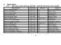
1
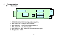
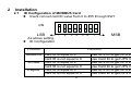
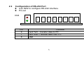
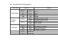
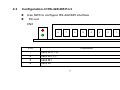
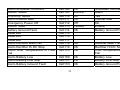
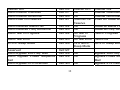
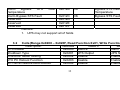
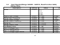
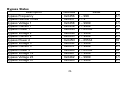
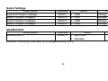
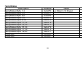
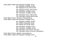
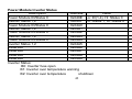
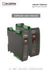
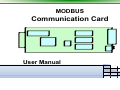
MODBUS
Communication Card
User Manual
1
1
Presentation
1.1
Overview
3
5
1
4
2
1. MODBUS Card ID configuration switch
2. RS-232 Port configuration switch
3. RS-422/485 Port configuration switch
4. RS-422/485 selection switch
5. RS-422/485 and RS-232 communication port
6. Diagnostic LEDs
2
6
1.2
Function
z
z
z
z
z
z
z
Provide UPS the functionality of communication with PC through MODBUS
protocol
Implementation of MODBUS RTU protocol
Provide MODBUS function including Read Coils/Discrete Inputs/Holding
Registers/Input Registers and Write Single Coil/Single Register
Provide RS-422/485 and RS-232 interfaces. PC can communicate with
UPS through RS-422/485 or RS-232 or both simultaneously.
Provide alarm LEDs, users can tell communication status quickly.
Except MODBUS protocol, also support 3Phase/Regular Protocols. Users
can select communication protocol through function switches.
Provide firmware upgrade functionality through RS-232 port.
3
2
Installation
2.1
ID Configuration of MODBUS Card
z Users can set card ID value from 0 to 255 through SW1.
ON
LSB
1
2
3
4
5 6
7
MSB
As above setting, card ID will be 1.
z ID Configuration
Protocol
Function
MODBUS Card ID is equal to 0
Card ID is not equal to 0
3Phase Card ID is equal to 0
Card ID is not equal to 0
Regular Card ID is equal to 0
Card ID is not equal to 0
4
Use UPS ID to get UPS Info
Use Card ID to get UPS Info
Use UPS ID to get UPS Info
Use Card ID to get UPS Info
Use UPS ID to get UPS Info
Use Card ID to get UPS Info
2.2
Configuration of RS-232 Port
z Use SW2 to configure RS-232 interface.
z Pin-out
CN3
8
Pin
6
7
8
7
6
5
4
Function
Card TxD – transfer data to PC
Card RxD – receive data from PC
GND
5
3
2
1
z
RS-232 Port Configuration
Function
Baud-rate
Parity
Check
Protocol
Switch
Value
SW2-1
SW2-2
OFF
OFF 2400
ON
OFF 4800
OFF
ON
9600
ON
ON
19200
OFF Disable Parity Check
SW2-3
ON
Enable Parity Check
OFF Even Parity
SW2-4
ON
Odd Parity
SW2-5
SW2-6
OFF
OFF MODBUS Protocol
ON
OFF Regular Protocol
OFF
ON
3Phase Protocol
SW2-7 Reserved
SW2-8 Reserved
6
2.3
Configuration of RS-422/485 Port
z
z
Use SW3 to configure RS-422/485 interface
Pin-out
CN3
8
Pin
1
2
3
4
7
6
5
4
Function
Card D+(T+)
Card D-(T-)
Card R+
Card R7
3
2
1
z
z
RS-485/RS-422 Selection
Switch
Setting
RS485
Enable RS-485
SW4
RS422
Enable RS-422
RS-422/485 Port Configuration
Function
Switch
SW3-1 SW3-2
Baud-rate
Parity
Check
Protocol
OFF
OFF
ON
OFF
OFF
ON
ON
ON
SW3-3
SW3-4
OFF
ON
OFF
ON
2400
4800
9600
19200
Disable Parity Check
Enable Parity Check
Even Parity
Odd Parity
SW3-5 SW3-6
8
Function
Value
OFF
OFF
ON
OFF
OFF
Termination
Resistor
SW3-7
SW3-8
ON
OFF
ON
OFF
ON
2.4
MODBUS Protocol
Regular Protocol
3Phase Protocol
Disable RS-485/422 Termination Resistor
Enable RS-485/422 Termination Resistor
Disable RS-422 Termination Resistor
Enable RS-422 Termination Resistor
LED Indicator
LED
Status
Red LED
Dark
Flashing(1 second)
Green LED Light 0.2 second
9
Description
UPS is disconnected
UPS is connected
When receive PC request
3
Operation
3.1
Discrete Inputs (Range 0x0100 – 0x012F, Read Function 0x02)
Description
Address
Value 0
Value 1
Alarm Temperature
0x0100 OK
Over Temperature
Alarm Input Bad
0x0101 OK
Input Bad
Alarm Output Bad
0x0102 OK
Output Bad
Alarm Overload
0x0103 OK
Overload
Alarm Bypass Bad
0x0104 OK
Bypass Bad
Alarm Output Off
0x0105 Output On
Output Off
Alarm UPS Shutdown
0x0106 OK
Shutdown
Alarm Charger Failure
0x0107 OK
Charger Failure
Alarm System Off
0x0108 System On
System Off
Alarm Fan Failure
0x0109 OK
Fan Failure
Alarm Fuse Failure
0x010A OK
Fuse Failure
Alarm General Fault
0x010B OK
General Fault
Alarm Awaiting Power
0x010C OK
Awaiting Power
Alarm Shutdown Pending
0x010D OK
Shutdown Pending
10
Alarm Shutdown Imminent
Buzzer Status
Economic Mode
Alarm Inverter Bad
Emergency Power Off
Buzzer State
Battery Ground Fault
Reserved
Reserved
Reserved
Alarm Rectifier Main Fail
Alarm Rectifier Hi DC Stop
Alarm Over Temperature or Fuse
Fail
Alarm Battery Low
Alarm Battery Low Stop
Alarm Battery Ground Fault
0x010E
0x010F
0x0110
0x0111
0x0112
0x0113
0x0114
0x0115
0x0116
0x0117
0x0118
0x0119
0x011A
OK
Silence
No
OK
Off
Disable
OK
Shutdown Imminent
Alarm
Yes
Inverter Bad
On
Enable
Battery Ground Fault
OK
OK
OK
0x011B
0x011C
0x011D
OK
OK
OK
Rectifier Main Fail
Rectifier Hi DC Stop
Over Temperature or Fuse
Fail
Battery Low
Battery Low Stop
Battery Ground Fault
11
Inverter ON
Alarm Inverter Overload
Alarm Inverter Abnormal
Alarm Load On Reserve
0x011E
0x011F
0x0120
0x0121
Inverter OFF
OK
OK
Load Not On
Reserve
OK
OK
No Test In
Progress
No Test Error
UPS Not In
Sleep Mode
Inverter ON
Inverter Overload
Inverter Abnormal
Load On Reserve
Alarm Reserve Mains Fail
Alarm Reserve Freq. Abnormal
Alarm Test In Progress
0x0122
0x0123
0x0124
Alarm Test Error
UPS In Sleep Mode
0x0125
0x0126
Reserved
Alarm Bypass Volt/Freq. Bad
Alarm Bypass Phase Sequence
Bad
Alarm Bypass STS Overload
0x0127
0x0128
0x0129
OK
OK
0x012A
OK
Bypass Volt/Freq. Bad
Bypass Phase Sequence
Bad
Bypass STS Overload
12
Reserve Mains Fail
Reserve Freq. Abnormal
Test In Progress
Test Error
UPS In Sleep Mode
Alarm
Bypass
STS
Over 0x012B OK
Temperature
Alarm Bypass STS Fault
0x012C OK
Reserved
0x012D
Reserved
0x012E
Reserved
0x012F
Remark:
1. UPS may not support all of fields
3.2
Bypass STS Over
Temperature
Bypass STS Fault
Coils(Range 0x0200 – 0x020F, Read Function 0x01, Write Function 0x05)
Description
Address
Value 0
Value 1
UPS Buzzer
0x0200 Silence
Alarm
Shutdown Type
0x0201 UPS Output
UPS System
Economic Mode Setting
0x0202 Disable
Enable
ATX PC Reboot Function
0x0203 Disable
Enable
AC Fail & Restore Auto-Reboot
0x0204 Disable
Enable
13
ATX PC Resume Function
Enable/Disable Buzzer
EPO Setting
Enable/Disable Inverter
Clear SRAM
Cancel Shutdown Restart
0x0205
0x0206
0x0207
0x0208
0x0209
0x020A
Set Output On/Off
0x020B
Reserved
0x020C
Reserved
0x020D
Reserved
0x020E
Reserved
0x020F
Remark:
UPS may not support all of fields
14
Disable
Disable
Disable
Disable
Clear SRAM
Cancel Shutdown
Restart
OFF
Enable
Enable
Enable
Enable
Clear SRAM
Cancel
Shutdown
Restart
ON
3.3
Holding Register(Range 0x0300 – 0x0321, Read Function 0x03, Write
Function 0x06)
Description
Address
Value
Unit
Shutdown Action
0x0300 0 – 9999(0=Abort)
Seconds
Shutdown Restart
0x0301 0 – 65535
Minutes
Test
0x0302 0 : Abort Test
1 : General Test
2 : BTV Test
3 : Test for 10 seconds
4 : Test until battery low
UPS Identification
0x0303 0 – 99
Low Transfer Voltage
0x0304 0 – 999
Voltage
High Transfer Voltage
0x0305 0 – 999
Voltage
Voltage Sensitivity
0x0306 0 : Normal
1 : Reduced
2 : Low
Last Battery Replace Date - Year
0x0307 0 – 9999
15
Last Battery Replace Date - Month
Last Battery Replace Date - Day
Next Battery Replace Date - Year
Next Battery Replace Date - Month
Next Battery Replace Date - Day
UPS Periodic Auto-Test
0x0308
0x0309
0x030A
0x030B
0x030C
0x030D
Buzzer Test
UPS Boot Delay
Bypass Freq. Tolerance
Select Output Voltage
Test Time
Test Voltage
Reserved
0x030E
0x030F
0x0310
0x0311
0x0312
0x0313
0x0314
16
1 - 12
1 - 31
0 – 9999
1 - 12
1 - 31
1 : Disable
2 : Daily
3 : Weekly
4 : Bi-Weekly
5 : Monthly
1 – 99
0 – 999
5 – 50
0 – 999
1 – 60
0 – 999
Seconds
Seconds
0.1Hz
Voltage
Minutes
Voltage
Reserved
0x0315
External Battery Pack
0x0316
Dry Contact W1
0x0317
Dry Contact W2
0x0318
Dry Contact W3
0x0319
Dry Contact W4
0x031A
Dry Contact W5
0x031B
Dry Contact W6
0x031C
Bypass Low Transfer Voltage
0x031D
Bypass High Transfer Voltage
0x031E
Bypass Voltage Tolerance
0x031F
Dry Contact Input Status 1
0x0320
Dry Contact Input Status 2
0x0321
Remark:
UPS may not support all of fields
17
0 - 10
0 - 999
0 - 999
0 - 999
Voltage
Voltage
Voltage
3.4
Input Register(Range 0x0400 – 0x051C, Read Function 0x04)
Rating Value
Description
Address
Value
Unit
Series
0x0400 0: T
1: H
2: NT
3: NH
Raging Input Voltage
0x0401 0 – 999
Voltage
Rating Input Frequency
0x0402 0 – 999
0.1Hz
Rating Output Voltage
0x0403 0 – 999
Voltage
Rating Output Frequency
0x0404 0 – 999
0.1Hz
Rating VA
0x0405 0 – 65534
10 VA
Rating Output Power
0x0406 0 – 65534
10 Watt
Low Battery Time
0x0407 0 – 99
Minutes
Low Tx Voltage Point
0x0408 0 – 999
Voltage
High Tx Voltage Point
0x0409 0 – 999
Voltage
Low Tx Voltage Upper Bound
0x040A 0 – 999
Voltage
18
Low Tx Voltage Lower Bound
High Tx Voltage Upper Bound
High Tx Voltage Lower Bound
UPS Type
0x040B
0x040C
0x040D
0x040E
Rating Battery Voltage
Low Tx Frequency Point
High Tx Frequency Point
Bypass Rating Frequency
Bypass Freq. Max Tolerance
Bypass Freq. Set Tolerance
Bypass Low Tx Voltage Point/Bypass
Rating Voltage
0x040F
0x0410
0x0411
0x0412
0x0413
0x0414
0x0415
19
0 – 999
0 – 999
0 – 999
0 : On-Line
1 : Off-Line
2 : Line-Interactive
3 : 3Phase
4 : Split Phase
5 : Others
0 – 999
0 – 999
0 – 999
0 – 999
5 – 50
5 – 50
0 – 999
Voltage
Voltage
Voltage
Voltage
0.1Hz
0.1Hz
0.1Hz
0.1Hz
0.1Hz
Voltage
Bypass High Tx Voltage Point
Bypass Low Tx Voltage Upper
Bound/Bypass Voltage Max
Tolerance
Bypass Low Tx Voltage Lower
Bound/Bypass Voltage Set Tolerance
Bypass High Tx Voltage Upper
Bound
Bypass High Tx Voltage Lower
Bound
Reserved
Reserved
Reserved
0x0416
0x0417
0 – 999
0 – 999
Voltage
Voltage
0x0418
0 – 999
Voltage
0x0419
0 – 999
Voltage
0x041A
0 – 999
Voltage
0x041B
0x041C
0x041D
20
Battery Status
Description
Battery Condition
Battery Status
Battery Charge
Seconds On Battery
Estimated Minutes Remaining
Estimated Charge Remaining
Battery Voltage
Battery Current
Address
Value
0x041E 0 : Good
1 : Weak
2 : Replace
0x041F 0 : OK
1 : Low
2 : Depleted
0x0420 0 : Floating
1 : Charging
2 : Resting
3 : Discharging
0x0421 0 – 65534
0x0422 0 – 9999
0x0423 0 – 999
0x0424 0 – 9999
0x0425 0 – 9999
21
Unit
Seconds
0.1Voltage
0.1Amp
Temperature
Battery Level
External Battery Pack #
Negative Battery Voltage
Negative Battery Current
Negative Battery Temperature
Negative Battery Level
Reserved
Reserved
Reserved
0x0426
0x0427
0x0428
0x0429
0x042A
0x042B
0x042C
0x042D
0x042E
0x042F
0 – 999
0 – 999
0 - 10
0 – 9999
0 – 9999
0 – 999
0 – 999
Degree Celsius
%
0.1Voltage
0.1Amp
Degree Celsius
%
Input Status
Description
Input Number Lines
Input Frequency 1
Input Voltage 1
Input Current 1
Address
0x0430
0x0431
0x0432
0x0433
22
Value
0–9
0 – 999
0 – 9999
0 – 9999
Unit
0.1Hz
0.1Voltage
0.1Amp
Input Power 1
Input Frequency 2
Input Voltage 2
Input Current 2
Input Power 2
Input Frequency 3
Input Voltage 3
Input Current 3
Input Power 3
Input Voltage 12
Input Voltage 23
Input Voltage 31
Reserved
Reserved
0x0434
0x0435
0x0436
0x0437
0x0438
0x0439
0x043A
0x043B
0x043C
0x043D
0x043E
0x043F
0x0440
0x0441
23
0 – 65534
0 – 999
0 – 9999
0 – 9999
0 – 65534
0 – 999
0 – 9999
0 – 9999
0 – 65534
0 – 9999
0 – 9999
0 – 9999
10 Watt
0.1Hz
0.1Voltage
0.1Amp
10 Watt
0.1Hz
0.1Voltage
0.1Amp
10 Watt
0.1Voltage
0.1Voltage
0.1Voltage
Output Status
Description
Output Source
Output Frequency
Output Number Lines
Output Voltage 1
Output Current 1
Output Power 1
Output Load1
Output Voltage 2
Address
Value
0x0442 0 : Normal
1 : Battery
2 : Bypass(Reserve)
3 : Reducing
4 : Boosting
5 : Manual Bypass
6 : Other
7 : None
0x0443 0 – 999
0x0444 0 – 9
0x0445 0 – 9999
0x0446 0 – 9999
0x0447 0 –65534
0x0448 0 – 999
0x0449 0 – 9999
24
Unit
0.1Hz
0.1Voltage
0.1Amp
10 Watt
%
0.1Voltage
Output Current 2
Output Power 2
Output Load 2
Output Voltage 3
Output Current 3
Output Power 3
Output Load 3
Output Voltage 12
Output Voltage 23
Output Voltage 31
Reserved
Reserved
0x044A
0x044B
0x044C
0x044D
0x044E
0x044F
0x0450
0x0451
0x0452
0x0453
0x0454
0x0455
25
0 – 9999
0 – 65534
0 – 999
0 – 9999
0 – 9999
0 – 65534
0 – 999
0 – 9999
0 – 9999
0 – 9999
0.1Amp
10 Watt
%
0.1Voltage
0.1Amp
10 Watt
%
0.1Voltage
0.1Voltage
0.1Voltage
Bypass Status
Description
Bypass Frequency
Bypass Number Lines
Bypass Voltage 1
Bypass Current 1
Bypass Power 1
Bypass Voltage 2
Bypass Current 2
Bypass Power 2
Bypass Voltage 3
Bypass Current 3
Bypass Power 3
Bypass Voltage 12
Bypass Voltage 23
Bypass Voltage 31
Address
0x0456
0x0457
0x0458
0x0459
0x045A
0x045B
0x045C
0x045D
0x045E
0x045F
0x0460
0x0461
0x0462
0x0463
26
Value
0 – 999
0–9
0 – 9999
0 – 9999
0 – 65534
0 – 9999
0 – 9999
0 – 65534
0 – 9999
0 – 9999
0 – 65534
0 – 9999
0 – 9999
0 – 9999
Unit
0.1Hz
0.1Voltage
0.1Amp
10 Watt
0.1Voltage
0.1Amp
10 Watt
0.1Voltage
0.1Amp
10 Watt
0.1Voltage
0.1Voltage
0.1Voltage
Bypass STS Temperature
0x0464
Reserved
Reserved
0x0465
0x0466
0 - 999
Degree
Celsius
Test Status
Description
Test Result
Address
Value
0x0467 0 : No Test Performed
1 : Test Passed
2 : Test in Progress
3 : General Test Fault
4 : Battery Test Fault
5 : Deep Battery Test
Fault
6 : Test Aborted
27
Unit
Output Relay
Description
Number of Output Relay
Address
Value
0x0468 0 : Not Available
> 0 : Available(<=99)
28
Unit
Environment
Description
Temperature
Humidify
Relay 1
Relay 2
Relay 3
Relay 4
Reserved
Reserved
Address
Value
0x0469 0 – 999
0x046A 0 – 999
0x046B 0 : Off
1 : On
0x046C 0 : Off
1 : On
0x046D 0 : Off
1 : On
0x046E 0 : Off
1 : On
0x046F
0x0470
29
Unit
Degree Celsius
Select Voltage
Description
Selected Output Voltage
Select Output Voltage1
Select Output Voltage2
Select Output Voltage3
Address
0x0471
0x0472
0x0473
0x0474
SRAM EXIST
Description
SRAM EXIST
Value
0 – 999
0 – 999
0 – 999
0 – 999
Address
Value
0x0475 0 : Not Exist
1 : Existed
Remark: Currently, this field is not supported by UPS
30
Unit
Voltage
Voltage
Voltage
Voltage
Unit
TempStatus
Description
TempStatus Byte 1,2
TempStatus Byte 3,4
TempStatus Byte 5,6
TempStatus Byte 7,8
TempStatus Byte 9,10
TempStatus Byte 11,12
TempStatus Byte 13,14
TempStatus Byte 15,16
TempStatus Byte 17,18
TempStatus Byte 19,20
Reserved
Reserved
Address
Value
0x0476 Lo: Byte1, Hi: Byte2
0x0477
0x0478
0x0479
0x047A
0x047B
0x047C
0x047D
0x047E
0x047F
0x0480
0x0481
31
Unit
Temp Byte1(Lo) : R Phase Inverter Temperature
Temp Byte2(Hi): B0: Temperature Warning(>=75C)
B1: High Temperature Shutdown(>=85C)
B2: Inverter Voltage too Low
B3: Inverter Voltage too High
B4: Overload Warning
B5: Overload Shutdown
B6: Inverter Fuse Fail Shutdown
B7: Inv. PCB communication abnormal
Temp Byte3(Lo): S Phase Inverter Temperature
Temp Byte4(Hi): B0: Temperature Warning(>=75C)
B1: High Temperature Shutdown(>=85C)
B2: Inverter Voltage too Low
B3: Inverter Voltage too High
B4: Overload Warning
B5: Overload Shutdown
B6: Inverter Fail Shutdown
B7: Parallel Communication Abnormal
Temp Byte5(Lo): T Phase Inverter
Temperature
32
Temp Byte6(Hi): B0: Temperature Warning(>=75C)
B1: High Temperature Shutdown(>=85C)
B2: Inverter Voltage too Low
B3: Inverter Voltage too High
B4: Overload Warning
B5: Overload Shutdown
B6: Inverter Freq. Abnormal Shutdown
B7: Parallel Communication Fail
Temp Byte7(Lo): B3 .. B0: The Summary of UPS Run at Inverter Test Mode
B7 .. B4: The Summary of UPS Run at Inverter Mode
Temp Byte8(Hi): B0: Power Fail
B1: EPO Happen
B2: MB_ON(To Bypass)
B3: Battery Low Warning
B4: Battery Low Shutdown
B5: Master UPS(Output Sync)
B6: Inverter DC Bus Abnormal Shutdown
B7: Short Circuit Happen Shutdown
Temp Byte9(Lo): Heatsink Temperature
33
Temp Byte10(Hi): B0: Bypass Voltage Over
B1: Bypass Voltage Under
B2: Bypass Freq. Abnormal
B3: Bypass Phase Abnormal
B4: Rectifier Voltage Over
B5: Rectifier Voltage Under
B6: Rectifier Freq. Abnormal
B7: Rectifier Phase Abnormal
Temp Byte11(Lo): Ambient Temperature
Temp Byte12(Hi): B0: Bypass Voltage Over
B1: Bypass Voltage Under
B2: SSW at Bypass Side
B3: SSW at Inverter Side
B4: Rectifier Voltage Over
B5: Rectifier Voltage Under
B6: Rectifier Input Over Current
B7: Rectifier Input Current Unbalance
Temp Byte13(Lo): Battery Temperature
Temp Byte14(Hi): B0: Bypass Voltage Over
34
B1: Bypass Voltage Under
B2: Low Battery Shutdown
B3: Low Battery Warning
B4: Rectifier Voltage Over
B5: Rectifier Voltage Under
B6: Rectifier Fail
B7: DC Bus Over Voltage
Temp Byte15(Lo): B0: TR1 Over Temperature(O/P TR Over Heat Shutdown)
B1: TR2 Input Choke Over Heat(I/P TR Over Heat Shutdown)
B2: Rectifier Over Temperature Warning(>=75C)
B3: Rectifier Over Temperature Shutdown(>=85C)
B4: Static Switch Over Temperature Warning(>=75C)
B5: Static Switch Over Temperature Shutdown(>=85C)
B6: Static Switch Overload
B7: Static Switch Fail
Temp Byte16(Hi): B0: Converter Board Power Abnormal
B1: EPO Happen
B2: Manual Bypass On
B3: Converter Board Communication Error
35
B4: Battery Cabinet Over Temperature Warning(>=75C)
B5: Battery Ground Fault
B6: Battery Test in Progress
B7: Battery Test Fail
Temp Byte17: Reserved
Temp Byte18: Reserved
Temp Byte19: Reserved
Temp Byte20(Hi): B5: Ambiance Over Temperature
B7: Auxiliary Power Fail
Remark:
1. Currently, TempStatus is not supported by UPS
36
Parallel Master ID
Description
Parallel Master ID
Address
0x0482 0 - 99
Available Event Log
Description
Address
UPS Event Log
0x0483 0 – 500
Event Log Report Format
0x0484 0 - 1
Event Reporting Method
0x0485 0 - 1
Event Log Report Format: 0: NT 9 byte format
1: NH 8 byte format
37
Value
Unit
Value
Unit
Power Module Attribute
Description
Address
Value
Unit
Power Module ID/Attribute
0x0486 Lo: ID(1-4), Hi: Attribute
Power Module ID/Attribute
0x0487
Power Module ID/Attribute
0x0488
Power Module ID/Attribute
0x0489
Reserved
0x048A
Reserved
0x048B
Power Module Attribute: which is used to identify the attribute of the power module.
B0: PFC
B1: Rectifier
B2: Charger
B3: Inverter
B4: Bypass
B5: TBD
B6: TBD
B7: TBD
38
Power Module General Status
Description
Address
Value
Power Module ID/ General Status
0x048C Lo: ID(1-4), Hi: Status
Power Module ID/ General Status
0x048D
Power Module ID/ General Status
0x048E
Power Module ID/ General Status
0x048F
Reserved
0x0490
Reserved
0x0491
Power Module General Status:
B0: The power module exist or the power module is powered
B1:
B2:
B3:
B4:
B5:
B6:
B7: Fault shutdown
39
Unit
Power Module PFC Status
Description
Address
Value
Power Module ID
0x0492 1-4
PFC Status 0,1
0x0493 Lo: Status 0, Hi: Status 1
Power Module ID
0x0494
PFC Status 0,1
0x0495
Power Module ID
0x0496
PFC Status 0,1
0x0497
Power Module ID
0x0498
PFC Status 0,1
0x0499
Reserved
0x049A
Reserved
0x049B
Reserved
0x049C
Reserved
0x049D
PFC Status:
B0: PFC fuse open shutdown
B1: PFC over temperature warning
B2: PFC over temperature shutdown
40
Unit
B3: DC bus over voltage warning
B4: DC bus over voltage shutdown
B5: DC bus under voltage warning
B6: DC bus under voltage shutdown
B7: PFC circuit general fault
B8: Fan failure
B9: TBD
B10: TBD
B11: TBD
B12: Inner communication failure
B13: TBD
B14: TBD
B15: Not calibrated (used to indicate whether the power module has been calibrated)
41
Power Module Inverter Status
Description
Address
Value
Power Module ID/Status 0
0x049E Lo: ID(1-4), Hi: Status 0
Inverter Status 1,2
0x049F Lo: Status 1, Hi: Status 2
Power Module ID/Status 0
0x04A0
Inverter Status 1,2
0x04A1
Power Module ID/Status 0
0x04A2
Inverter Status 1,2
0x04A3
Power Module ID/Status 0
0x04A4
Inverter Status 1,2
0x04A5
Reserved
0x04A6
Reserved
0x04A7
Reserved
0x04A8
Reserved
0x04A9
Inverter Status:
B0: Inverter fuse open
B1: Inverter over temperature warning
B2: Inverter over temperature
shutdown
42
Unit
B3: Fan failure
B4:
B5: Inverter short circuit
B6: Inverter STS failure
B7: Inverter voltage abnormal
B8: Inverter circuit general fault
B9: DC bus over voltage shutdown
B10: Inverter overload
B11:
B12: Inner communication loss (includes the comm. to system or other modules)
B13: EPO shutdown
B14: Inverter parallel communication loss
B15: Inverter parallel failure (which may due to any of ID, or rating setting conflict,
etc…)
B16: TBD
B17: TBD
B18: TBD
B19: TBD
B20: TBD
43
B21: TBD
B22: TBD
B23: Not calibrated (used to indicate whether the power module has been
calibrated)
44
Power Module Charger Status
Description
Address
Value
Power Module ID/ Charger Status
0x04AA Lo: ID(1-4), Hi: Status
Power Module ID/ Charger Status
0x04AB
Power Module ID/ Charger Status
0x04AC
Power Module ID/ Charger Status
0x04AD
Reserved
0x04AE
Reserved
0x04AF
Charger Status:
B0: Charger circuit general fault
B1-B7: Reserved
45
Unit
Power Module Temperature Status
Description
Power Module ID
Temperature PFC
Temperature TBD
Temperature INV
Temperature INV R
Temperature INV S
Temperature INV T
Power Module ID
Temperature PFC
Temperature TBD
Temperature INV
Temperature INV R
Temperature INV S
Temperature INV T
Power Module ID
Address
0x04B0
0x04B1
0x04B2
0x04B3
0x04B4
0x04B5
0x04B6
0x04B7
0x04B8
0x04B9
0x04BA
0x04BB
0x04BC
0x04BD
0x04BE
46
Value
1-4
0 – 9999
0 – 9999
0 – 9999
0 – 9999
0 – 9999
0 – 9999
1-4
0 – 9999
0 – 9999
0 – 9999
0 – 9999
0 – 9999
0 – 9999
1-4
Unit
0.1Voltage
0.1Voltage
0.1Voltage
0.1Voltage
0.1Voltage
0.1Voltage
0.1Voltage
0.1Voltage
0.1Voltage
0.1Voltage
0.1Voltage
0.1Voltage
Temperature PFC
Temperature TBD
Temperature INV
Temperature INV R
Temperature INV S
Temperature INV T
Power Module ID
Temperature PFC
Temperature TBD
Temperature INV
Temperature INV R
Temperature INV S
Temperature INV T
Reserved
Reserved
Reserved
Reserved
0x04BF
0x04C0
0x04C1
0x04C2
0x04C3
0x04C4
0x04C5
0x04C6
0x04C7
0x04C8
0x04C9
0x04CA
0x04CB
0x04CC
0x04CD
0x04CE
0x04CF
47
0 – 9999
0 – 9999
0 – 9999
0 – 9999
0 – 9999
0 – 9999
1-4
0 – 9999
0 – 9999
0 – 9999
0 – 9999
0 – 9999
0 – 9999
0.1Voltage
0.1Voltage
0.1Voltage
0.1Voltage
0.1Voltage
0.1Voltage
0.1Voltage
0.1Voltage
0.1Voltage
0.1Voltage
0.1Voltage
0.1Voltage
Reserved
Reserved
Reserved
Reserved
Reserved
Reserved
Reserved
Reserved
Reserved
Reserved
0x04D0
0x04D1
0x04D2
0x04D3
0x04D4
0x04D5
0x04D6
0x04D7
0x04D8
0x04D9
48
Power Module Inverter Voltage
Description
Address Value
Power Module ID
Inverter Voltage R
Inverter Voltage S
Inverter Voltage T
Power Module ID
Inverter Voltage R
Inverter Voltage S
Inverter Voltage T
Power Module ID
Inverter Voltage R
Inverter Voltage S
Inverter Voltage T
Power Module ID
Inverter Voltage R
0x04DA
0x04DB
0x04DC
0x04DD
0x04DE
0x04DB
0x04DC
0x04DD
0x04DE
0x04DF
0x04E0
0x04E1
0x04E2
0x04E3
49
1–4
0 – 9999
0 – 9999
0 – 9999
1–4
0 – 9999
0 – 9999
0 – 9999
1–4
0 – 9999
0 – 9999
0 – 9999
1–4
0 – 9999
Unit
0.1Voltage
0.1Voltage
0.1Voltage
0.1Voltage
0.1Voltage
0.1Voltage
0.1Voltage
0.1Voltage
0.1Voltage
0.1Voltage
Inverter Voltage S
Inverter Voltage T
Power Module ID
Inverter Voltage R
Inverter Voltage S
Inverter Voltage T
Reserved
Reserved
Reserved
Reserved
Reserved
Reserved
Reserved
Reserved
0x04E4
0x04E5
0x04E6
0x04E7
0x04E8
0x04E9
0x04EA
0x04EB
0x04EC
0x04ED
0x04EE
0x40EF
0x04F0
0x04F1
50
0 – 9999
0 – 9999
1–4
0 – 9999
0 – 9999
0 – 9999
0.1Voltage
0.1Voltage
0.1Voltage
0.1Voltage
0.1Voltage
Battery Cabinet Temperature
Description
Battery Cabinet #1 Temperature
Battery Cabinet #2 Temperature
Battery Cabinet #3 Temperature
Battery Cabinet #4 Temperature
Reserved
Reserved
Address
0x04F2
0x04F3
0x04F4
0x04F5
0x04F6
0x04F7
51
Value
0 – 999
0 – 999
0 – 999
0 - 999
Unit
Degree Celsius
Degree Celsius
Degree Celsius
Degree Celsius
Manufacture
Description
Manufacture Byte 0, 1
Manufacture Byte 2, 3
Manufacture Byte 4, 5
Manufacture Byte 6, 7
Manufacture Byte 8, 9
Manufacture Byte 10, 11
Manufacture Byte 12, 13
Manufacture Byte 14, 15
Reserved
Reserved
Reserved
Address
0x04F8
0x04F9
0x04FA
0x04FB
0x04FC
0x04FD
0x04FE
0x04FF
0x0500
0x0501
0x0502
52
Value
Lo: Byte0, Hi: Byte 1
Lo: Byte2, Hi: Byte 3
Lo: Byte4, Hi: Byte 5
Lo: Byte6, Hi: Byte 7
Lo: Byte8, Hi: Byte 9
Lo: Byte10, Hi: Byte 11
Lo: Byte12, Hi: Byte 13
Lo: Byte14, Hi: Byte 15
Unit
Model
Description
Model Byte 0, 1
Model Byte 2, 3
Model Byte 4, 5
Model Byte 6, 7
Model Byte 8, 9
Model Byte 10, 11
Model Byte 12, 13
Model Byte 14, 15
Reserved
Reserved
Reserved
Address
0x0503
0x0504
0x0505
0x0506
0x0507
0x0508
0x0509
0x050A
0x050B
0x050C
0x050D
53
Value
Lo: Byte0, Hi: Byte 1
Lo: Byte2, Hi: Byte 3
Lo: Byte4, Hi: Byte 5
Lo: Byte6, Hi: Byte 7
Lo: Byte8, Hi: Byte 9
Lo: Byte10, Hi: Byte 11
Lo: Byte12, Hi: Byte 13
Lo: Byte14, Hi: Byte 15
Unit
Firmware Version
Description
Firmware Version Byte 0, 1
Firmware Version Byte 2, 3
Firmware Version Byte 4, 5
Firmware Version Byte 6, 7
Firmware Version Byte 8, 9
Firmware Version Byte 10, 11
Firmware Version Byte 12, 13
Firmware Version Byte 14, 15
Reserved
Reserved
Reserved
Address
0x050E
0x050F
0x0510
0x0511
0x0512
0x0513
0x0514
0x0515
0x0516
0x0517
0x0518
54
Value
Lo: Byte0, Hi: Byte 1
Lo: Byte2, Hi: Byte 3
Lo: Byte4, Hi: Byte 5
Lo: Byte6, Hi: Byte 7
Lo: Byte8, Hi: Byte 9
Lo: Byte10, Hi: Byte 11
Lo: Byte12, Hi: Byte 13
Lo: Byte14, Hi: Byte 15
Unit
CPU
Description
CPU Byte 0, 1
CPU Byte 2, 3
Reserved
UPS Connection Status
Description
UPS Connection Status
Address
Value
0x0519 Lo: Byte0, Hi: Byte 1
0x051A Lo: Byte2, Hi: Byte 3
0x051B
Unit
Address
Value
0x051C 0:Disconnection
1:Connection
Unit
Remark:
1. Filed value 0xFFFF in Input Registers represents that field is not supported by UPS
55