1
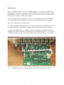
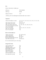
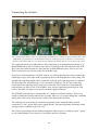
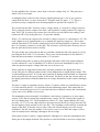
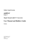
Oakley Sound Systems
5U Oakley Modular Series
midiDAC
Single Channel midiCV Converter
PCB Issue 4
Builder’s Guide
V4.0.4
Tony Allgood B.Eng PGCE
Oakley Sound Systems
Carlisle
United Kingdom
Introduction
This is the Builder's Guide for the issue 4 midiDAC midi to CV convertor 5U module from
Oakley Sound. This document contains a basic introduction to the board, a full parts list for
the components needed to populate the boards, a circuit description, and a list of the various
interconnections needed to make up the module.
For the User Manual which contains an overview of the operation of the unit, the midiDAC
PIC specifications and the calibration procedure, please visit the main project webpage at:
http://www.oakleysound.com/mididac.htm
For general information regarding where to get parts and suggested part numbers please see
our useful Parts Guide at the project webpage or http://www.oakleysound.com/parts.pdf.
For general information on how to build our modules, including circuit board population,
mounting front panel components and making up board interconnects please see our generic
Construction Guide at the project webpage or http://www.oakleysound.com/construct.pdf.
The issue 4 midiDAC fitted to a 2U wide natural finish Schaeffer MOTM format panel. The smaller board
mounted connectors are 0.1” Molex KK. The jack sockets are Switchcraft 112APCX.
2
The Printed Circuit Board
The PCB has been designed to fit within a 2U across MOTM style modular face plate. The
size of the board is slightly smaller than older issues at 13.4 cm high and 11.1 cm deep. It has
three PCB mounted pots to facilitate tune, bend depth and slide rate. The pots are spaced at
the standard Oakley and MOTM spacing of 1.625".
The switches and LEDs are typically hand wired directly to the PCB. The various sockets
used by the module typically use 0.1” KK Molex or MTA headers, however, they may be also
be wired directly into the board if you wish.
Midi channel is selected by four lines in ‘traditional’ binary fashion. Thus midi channel can be
switched by either onboard DIP switches or links, or by a 16 position rotary HEX switch
mounted on the front panel. I tend not to change midi channel once I have built the unit, so I
use DIP switches only. Because of this, there is no midi channel selector on the suggested
front panel layout. However, the board is equipped to take a 0.1” header to allow simple
connection to a rotary HEX switch.
The issue 4 PCB is double sided, has through plated holes, solder mask both sides and has full
component legending. All boards sold by us are Pb free and RoHS compliant but may be
soldered with Pb/Sn solder if you wish. Be aware that some of the resistors have their
legending underneath the component. So once the resistor is in place it does make it difficult
to identify the part’s name. This had to be done to reduce the board surface area. However, all
parts are labelled in a systematic fashion so that the smaller numbers are furthest left.
Power is admitted to the board via 0.156" Molex connector for MOTM/Oakley or 0.1” MTA
connector for fitting into Synthesizer.com systems.
The PCB has four mounting holes, one in each corner. However, using the midiDAC with the
recommended pots and brackets, will give you sufficient support without the need for
additional mounting hardware. The pots on the issue 4 midiDAC board are now 16mm Alps
or Alpha types.
3
Components
For general information regarding where to get parts and suggested part numbers please see
our useful Parts Guide at the project webpage or http://www.oakleysound.com/parts.pdf.
Some special considerations for this project:
Many of the resistors are 1/4W 5% or better types. Although there are some 1% and 0.1%
resistors listed. I would generally recommend 1% metal film types throughout except where
0.1% are specified.
The MAX551ACPA is available from Maxim direct, although they may have minimum order
quantities in your country. It may be even possible to request one as a one off sample.
Alternatively, the DAC is also available from Mouser their part number: 700-MAX551ACPA.
The midi channel selection is performed by a 4 way DIP switch. These are available in many
different types, but get the ones with 0.3” spacing between the rows. Avoid the piano key
style ones, since they can be very confusing... er, which way is on? Fit the switches so that
switch one is towards the bottom of the board. LSB is then switch one.
Some of the op-amps are not your ordinary TL072 type and there is a good reason to use the
ones specified. The LT1013 is a low offset bipolar op-amp. It may be substituted with a
OPA2277. The AD712JN is a low offset FET op-amp. This has a high impedance, low bias
current and high speed and is well suited for the DAC output amplifier and slide circuitry. The
LF412 is a fairly standard dual FET op-amp with a good enough performance in sample and
hold applications.
The HEF4104BP is a four channel low to high level shifter.
The REF02 is a 5V reference. Get the cheapest one in DIL or DIP form on offer.
The crystal is a 4MHz type. Low profile ones can be used and look neat and tidy. It is
probably best not to allow the crystal's casing to sit flat against the top side of the board
directly. So either use one of those small spacers designed for the job or simply solder the
crystal in place with a 2mm air gap between the base of the package and the surface of the
PCB.
4
Parts List
For general information regarding where to get parts and suggested part numbers please see
our useful Parts Guide at the project webpage or http://www.oakleysound.com/parts.pdf.
The components are grouped into values, the order of the component names is of no particular
consequence.
A quick note on European part descriptions. R is shorthand for ohm. K is shorthand for kiloohm. R is shorthand for ohm. So 22R is 22 ohm, 1K5 is 1,500 ohms or 1.5 kilohms. For
capacitors: 1uF = one microfarad = 1000nF = one thousand nanofarad.
To prevent loss of the small ‘.’ as the decimal point, a convention of inserting the unit in its
place is used. eg. 4R7 is a 4.7 ohm, 4K7 is a 4700 ohm resistor, 6n8 is a 6.8 nF capacitor.
Resistors
All values are 5% carbon or metal film ¼ W or better except those listed as 1% or 0.1%.
These must be 1% metal film and 0.1% metal film respectively.
75R
100R
220R
680R
1K
2K2
3K3
4K7
10K
10K, 1%
10K, 0.1%
11K
22K
33K, 1%
47K
100K
390K, 1%
R27, R19
R54, R55
R46, R53, R37
R11, R2, R17
R52, R47, R49, R33, R10, R41, R50, R43, R9, R48
R51
R26
R30, R31, R7, R22, R38, R40, R42, R45
R24, R29, R36, R28
R3, R20, R21, R6
R39, R44, R23, R25
R15
R8, R13
R18
R5, R1, R12, R35
R14, R16
R4
For +5V gate output (recommended): Make R34 a 10K resistor and omit R32
For +15V gate output: Make R32 a 10K resistor and omit R34.
Trimmers
2K Multiturn cermet
100K Multiturn cermet
V/OCT
INIT
5
Pots
All pots 16mm Alps or Alpha types.
47K linear
250K log*
TUNE, BEND
SLIDE
Alpha pot brackets
2 off
*100K log can be used although the maximum slide time is reduced.
Capacitors
100nF axial multilayer ceramic
18pF 2.5mm C0G ceramic
33pF 2.5mm C0G ceramic
10nF, 63V polyester box 5mm
1u5, 50V/63V polyester box 5mm
1uF, 63V electrolytic
2u2, 63V electrolytic
22uF, 35V electrolytic
47u, 35V electrolytic
C15, C32, C5, C6, C36, C4, C12, C30, C3, C23, C20,
C21, C11
C26, C25, C19
C13, C8, C7
C1, C31, C27, C33, C28, C34, C29
C2
C10
C22, C9, C18, C17, C14, C24
C35
C16
Discrete Semiconductors
1N4001 silicon diode
1N4148 signal diode
BAT42 schottky diode
BC550 small signal NPN transistor
5mm LED of any colour
D3, D8, D9, D10
D5, D6
D2, D4, D7
Q1, Q2
GATE, LEG
D1 is not fitted and the space is left empty.
Integrated Circuits
16F628 midiDAC PIC
CD4051B 1-8 mpx
CD4066B analogue switch
HEF4104BP level shifter
6N137 optocoupler
74HC04 Hex invertor
78L05 +5V regulator
AD712 Dual FET op-amp
LF412 Dual FET op-amp
U10
U14
U5
U15
U7
U6
U11
U4, U8
U12
6
MAX551ACPA 12-bit DAC
LT1013CP
REF-02 Precision 5V reference
TL084 or TL074 quad FET op-amp
U9
U1, U2
U3
U13
Connectors
MTA156 4 way header
MTA100 6-way header
PWR – Oakley/MOTM power supply
PWR2 – Synthesizers.com power supply
5-way 0.1” header and socket
4-way 0.1” header and socket
3-way 0.1” header and socket
2-way 0.1” header and socket
CN1
CN2
THRU, BUS
IN
Miscellaneous
4MHz Crystal (parallel resonant)
FERRITE
X1
L1, L2, L3, L4
LED lens and clips
SPDT or SPST toggle switches
4-way DIP switch
Knobs
1/4” sockets
5-pin midi sockets
Two off, colours to suit choice of LEDs
Two off, one for Trigger and one for Slide
One off
Three off
Eight off
Two off
Suitable lengths of insulated multistrand wire for interconnects.
You may well want to use sockets for the ICs. I would recommend low profile turned pin
types as these are the most reliable. You need eight 8-pin DIL, three 14-pin DIL, two 16-pin
DIL, and one 18-pin DIL.
7
Connecting the LEDs
The two LEDs should be connected first since it can get quite tricky to get to them once the
sockets are fitted.
LEDs have two pins and they must be fitted the correct way around otherwise the LED will
not light. Pin 1, the square pad, should go to the anode of the LED. And pin 2 to the cathode.
The way I wired my LEDs is to have the gate LED directly attached the PCB with its own
leads, and the slide LED using flying wires attached to a 0.1” Molex KK connector which
simply slips over the leads of the LED.
Attach the board to the panel and secure with the pot nuts. Then fit the gate LED into its clip
and trim off the leads so that they are just long enough to lie across the GATE solder pads.
Then ensuring that the leads are making contact with the pads solder them in place.
The slide LED can be wired in the usual fashion of using fly wires. I tend to use Molex KK
housings and crimps simply because it keeps things tidy and means you don't have to solder
or insulate the LED's leads.
8
Connecting the Switches
The two switches can now be wired to the panel. These require short lengths of wire to
connect them to the board. A standard SPDT switch has three solder tags. You will need to
connect the two pads on the board to the top two tags on the relevant switch. The lower tag
on each switch is left unconnected.
It doesn’t matter which wire goes to which tag, the main thing is that each switch gets the
correct pair of wires.
9
Connecting the Sockets
The top four output sockets. These are Switchcraft 112APCX types normally used for soldering direct into
PCBs but here used with wires and heatshrink. Note the earth lugs of each socket have been connected
together with 0.9mm solid core wire and connected back to the board with one wire from the top socket.
The suggested layout uses eight sockets, and wiring them up is straightforward enough. Use
multistrand hook up wire to connect each socket’s signal lug to the relevant pad on the PCB.
Keep your wires short but not too short and use as many different colour wires as you can.
There is no need to use screened cable for such short runs.
If you have used Switchcraft 112APCX sockets you will see that they have three connections
called lugs or tags. One is the earth or ground tag next to the diagonal part of the casing. The
second is the signal tag which will be connected to the tip of the jack plug when it is inserted.
The third tag is the normalised tag, or NC (normally closed) lug. The NC lug is internally
connected to the signal tag when a jack is not connected. This connection is automatically
broken when you insert a jack. The midiDAC uses only the signal and ground lugs on each
socket. The other two lugs are not used at all in the suggested layout.
The PCB has been laid out to accommodate 0.1” headers for all interconnects. This is very
useful for taking the board in and out for servicing. However, for a panel fitting into a modular
synth, there is no reason why you can’t solder wires directly into the holes.
The earth lugs of each socket are connected to ground via the standard Oakley ground
connection, ie. Pin 3 on the PSU power supply header. This special ground, sometimes called
'panel ground' is available at pin 5 on CN1.
The sockets' ground lugs can be connected together with one piece of solid core wire. I prefer
to use 0.9mm diameter wire because of its stiffness and low resistance.
10
The signal lugs of each 1/4” socket is connected up as follows:
Socket name
Header
Pin
Pitch
Velocity
Bender
Modulation
Aftertouch
CC
Gate
Slide
CN1
CN1
CN2
CN2
CN2
CN2
CN1
CN1
1
2
4
2
1
3
3
4
The MIDI sockets require careful attention. If you get the connection around the wrong way,
a lot of confusion will result.
For the MIDI IN connector: pin 1 on the PCB goes to pin 5 on the 5-pin DIN. Note that pin 5
is marked on the socket and is NOT the fifth pin on the socket. Pin 2 on the PCB goes to pin 4
on the DIN plug.
For the MIDI OUT connector: pin 1 on the PCB goes to pin 5 on the DIN plug, pin 2 on the
PCB goes to pin 2 of the DIN plug, pin 3 on the PCB goes to pin 4 on the DIN plug. On the
PCB pin 1 is always depicted by a square pad.
If you have a problem with the midiDAC it is most likely that you have wired up the midi in
socket incorrectly.
Figure 1. An internal view of the standard MIDI plug. Picture courtesy of Philip Rees Ltd.
11
Power supply connections
Power connections – MOTM and Oakley
The PSU power socket is 0.156” MTA 4-way header. Friction lock types are recommended.
This system is compatible with MOTM systems.
Power
Pin number
+15V
Module GND
Earth/PAN
-15V
1
2
3
4
The earth/pan connection has been provided to allow the ground tags of the jack sockets to be
connected to the powers supply ground without using the module’s 0V supply. Earth loops
cannot occur through patch leads this way, although screening is maintained. Of course, this
can only work if all your modules follow this principle.
Power connections – Synthesizers.com
The PWR power socket is to be fitted if you are using the module with a Synthesizers.com
system. In this case you should not fit the PSU header. The PWR header is a six way 0.1”
MTA, but with the pin that is in location 2 removed. In this way location 3 is actually pin 2 on
my schematic, location 4 is actually pin 5 and so on.
Power
Location number
Schematic Pin number
+15V
Missing Pin
+5V
Module GND
-15V
Not connected
1
2
3
4
5
6
1
2
3
4
5
+5V is not used on this module, so location 3 (pin 2) is not actually connected to anything on
the PCB.
If fitting the PWR header, you will also need to link out pins 2 and 3 of PSU. This connects
the panel ground with the module ground. Simply solder a solid wire hoop made from a
resistor lead clipping to join the middle two pads of PSU together.
12
Circuit Description
The midi data is electrically isolated by U7, a high speed logic output opto-coupler. The
output of U3 is pulled up via R43 and drives two circuits. One is the PIC, the processing
engine of the midi interface. The other is the midi THRU circuit. The latter is a circuit that
simply copies the data seen on the MIDI input port and presents it to the midi thru output
socket if one is fitted. U6 is a simple logic inverter gate, and two of these inverting gates in
series produce a buffered version of the opto’s output signal. Although U6 hardly affects the
signal at all, it does give it a current boost allowing it to drive the midi lines via the standard
220R resistors.
Notice the midi out connector requires the middle pin to be grounded for shielding purposes.
This is not allowed by the midi specification for the midi input socket, so grounding should
only be provided on the thru socket.
The heart of the midiDAC is a preprogrammed PIC16F628. This is where Trevor’s firmware
is located. X1, a 4 MHz crystal provides the necessary timing for the PIC’s internal oscillator.
For more details on the operating system of the PIC see the ‘Firmware Data’ section in the
User Manual.
Three of the PIC’s output lines directly drive a 12-bit DAC, U9. The DAC is driven serially,
and this is different to the older issue midiDAC where we used a parallel loading DAC.
Although, the DAC is a 12 bit device we actually only use 7 bits. The other 5 bits of data are
held low at the appropriate time in serial data stream.
Why use only the top seven? Firstly, midi data is arranged, in the main, in blocks of seven bits.
For example there are only 128 notes that a normal midi keyboard can send out. Secondly, the
PIC does not perform any CV scaling or tuning. This is sometimes used on other midi-CV
converters to generate ADSR and pitch bend information that is then merged in the digital
domain to the pitch data. 14 or 16 bit DACs are required for this. In the midiDAC all of our
CV processing is done in analogue hardware.
So why not use an eight bit DAC? With an 8-bit device, although it gives us 256 steps to play
with, the absolute accuracy of those steps is typically plus and minus 1/512 of the highest
output voltage of the DAC. That is an error of around +/- 0.2%. This may not sound much but
it does matter. In musical terms this means that the pitch difference between one pair of
adjacent notes will be different to the pitch difference between another pair. In other words,
when using a typical eight bit DAC which is specified to 0.5LSB accuracy, the notes played on
your keyboard will be noticeably out of tune. Tim Orr, of EMS fame, reckoned that at least
10-bit accuracy was required for users not to hear any difference in the steps. In the midiDAC
I have chosen to use 12-bits, because 12 bit DACs are affordable and easily available. The
errors in a good 12-bit DAC, at around +/-0.01%, will probably be negligible compared to
VCO tracking errors.
The MAX551 is a current output multiplying DAC. This means two other things are needed to
get it to convert digital data to an analogue voltage. Firstly, you need a very accurate
reference voltage. This will set the maximum output voltage that the DAC circuit will supply.
13
For the midiDAC the reference comes from a reference voltage chip, U3. This generates a
stable 5.00V at its output.
A multiplying DAC will invert the reference signal applied at pin 19. So to get a positive
output from our DAC, we have invert the 5V reference with U2 (pins 1, 2, 3). This is a
precision op-amp, configured as an inverting amplifier to produce the required -5V.
The second item the DAC needs to create a voltage output, is a current to voltage convertor.
This is strapped onto the output of the DAC, and in practice it simply consists of a single opamp. This is U8. It needs to be accurate, have low drift over time and be fast settling. I have
chosen an AD712 by Analog Devices. C19 provides stability.
With a -5V reference the output of the current to voltage convertor is a maximum of +5V. We
need a higher level of signal than this, so we amplify the signal by exactly two. This is done
with the other half of U8, which is configured as a non inverting amplifier of gain two. Notice
the 0.1% tolerance resistors to set the gain. This is because we need to have accuracy here so
that our pitch bend circuit works correctly.
The alert reader may well point out that we could have obtained a full scale output of 10V by
providing the DAC with a -10V reference. This is true, but the datasheet for the MAX551
hints that best performance is obtained with a -5V reference.
C13 and R42 allows the op-amp to drive the high capacitance load of the sample and hold
circuits without DC error or instability. D7 is there to protect the demultiplexer chip, U14,
from any spurious negative voltages that may occur on power up.
Notice, that the op-amps and reference have separate grounds to the digital parts of the
circuit. They have a different symbol on the circuit diagram like an upside down triangle. This
is called 'analogue ground’. It is at the same potential as digital ground and both are connected
at the star point close the power header on the board. The theory is that any current spikes on
the digital ground do not manifest themselves as voltage fluctuations on the sensitive analogue
ground.
The DAC’s output is constantly varying. All six CV outputs, which are controlled by a stream
of 12-bit data from the PIC, are represented by this fluctuating output. Each output has its
own time slot and this gives rise to a waveform that has six distinct sections that continuously
repeat, once every 4000th every second.
The demultiplexer based around U14 will direct each of these six outputs to its own output
section. U14 is like an electrically controlled rotary switch. The PIC controls this switch via
the level shifting chip, U15. The demultiplexer needs a 15V logic signal whilst the PIC only
provides +5V. U15 is a one chip solution to this and converts the low level logic from the PIC
into the high level logic needed to drive the 4051. The switching is tied in directly to match the
output of the DAC so that the correct order of the time slotted output goes to the correct
destination. The PIC also only enables U14 in such a way so as to allow the output of U8 to
settle accurately before allowing it through to the next stage.
Each output section is called a ‘sample and hold’, although to be strict the demultiplexer also
forms part of the sample and hold. The capacitor in each S/H holds or stores the voltage that
14
is briefly connected to it. The op-amp that is connected to it, allows this voltage to be ‘sniffed’
without effecting the actual value. The op-amps are connected as voltage followers or buffers.
They have gain of 1. Thus, the sampled voltage on the hold capacitors can be found at the
output of each op-amp. Note, that pitch CV and pitch bend use low offset FET op-amps, U12,
for accurate pitch control.
Note that not all of the eight outputs from the demultiplexer are connected to S/H circuits.
The PIC only processes six midi controllers so the other two outputs are unused.
The pitch and pitch bend CV are processed further by the midiDAC. This circuitry is seen on
page two of the schematics.
The pitch CV is sent to the slide circuit. This circuit is based heavily on the slide circuit from
the TB303, and, of course, the Oakley 3031. When the slide is not enabled, the first portion of
the analogue switch, U5, is off. The pitch CV is then passed through the slide pot straight to
the op-amp buffer, U4 (pins 1, 2, 3). The resistance of the slide pot has no effect on the CV
because the input impedance of the buffer is very, very high. The second portion of U5 is on,
and the capacitor, C2 is charged up to the CV voltage. Slide is activated, either by the PIC via
the SLD logic line, or manually via the ‘SLID’ header being shorted by the SLIDE switch.
This then causes the two sections of U5 swap states. The pitch CV now has to charge C2, via
the slide pot, every time the CV changes. The higher the resistance of the slide pot, the longer
it takes to charge up or down.
The slide signal from the PIC also drives the ‘legato’ LED via U6. The LED is connected to a
2 pin header on the PCB, labelled ‘LEG’.
The pitch bend CV varies from 0 to 10V depending on the status of the pitch bend controller.
For normal use, we require the pitch bend to go from -5V to +5V, with 0V representing the
pitch bend wheel centralised. To do this we must subtract exactly 5V from our pitch bend CV
signal.
This is done with a simple summing amplifier based around U2 (pins 5, 6, 7). This adds the
-5V reference voltage to the pitch CV. Since the pitch CV is centralised at +5V, when we add
these two voltages together, they cancel. However, a positive (upwards) bend produces a
negative voltage so we must invert the summed output with another op-amp circuit. This is
based around U4 (pins 5, 6,7) and features capacitive loading protection via R28 and C8. The
output of this circuit goes to the Pitch bend output socket and the Pitch Bend depth pot.
The Pitch bend depth pot allows a fraction of the pitch bend CV to be added to the pitch CV.
Thus wiggling the pitch bender will automatically control the pitch of any connected VCOs.
The circuitry based around both halves of U1 add the pitch bend CV to the pitch CV and to
allow fine tuning of the VCO pitch.
Note the use of 0.1% resistors in the summing circuit. If ordinary 5% resistors were used here,
it is likely that the -5V and the +5V signals would not be exactly cancelled. This would result
in a small error voltage, ie. non zero, at the pitch bend output.
Two forms of setting the initial pitch CV are provided. One is the TUNE pot mounted on the
front of the panel. The other is INIT, which is a multiturn trimmer that will allow precise
15
setting of the initial pitch CV, and thus aid centralising the TUNE pot’s range. In this version
of the midiDAC, the pot and trimmer take their end voltages from the +5V and -5V reference
voltages. This should lead to greater stability of the CV output even if the power supplies
change slightly.
There are 12 notes in one octave, and a jump of 1V must represent one octave when applied
to a VCO. Thus, 1/12 = 0.083333V or 83.33mV per semitone step with a perfect DAC. There
are 128 notes in the midi scale but if the lowest note is considered at starting at zero volts the
highest voltage must be 127 x 83.3mV = 10.58V.
With a -5V reference the smallest step our DAC will increment is only 78.7mV, so we need to
amplify up the pitch CV by around 1.06 to get the desired 83.3mV stepping. This is done in
the first summing circuit. The V/OCT trimmer allows to fine tune this gain to match your
midiDAC to your VCO’s sensitivity.
The PIC generates the gate signal directly from on if its outputs. It actually an inverted gate to
allow the main gate output to be generated by a single NPN transistor, Q2. The collector may
be wired to either the +5V or the +15V rail depending on the size of the gate signal required.
The GATE LED is connected to a 2 pin header on the PCB, labelled ‘Gate’. It is driven by a
spare gate within the inverter chip, U6. Note that if you use the suggested layout, the LED
may be mounted straight into the board for a tidy appearance.
U11 provides the regulated +5V supply for the PIC and DAC. R54 and C16 provide power
supply decoupling from the higher +15V rail. The four ferrites on the board, L1 to 4, act as
high frequency suppression to remove any digital noise from the power supply. The level
shifting chip, U15 and the demultiplexer, U14 also have their own decoupled and filtered
supply. This is to prevent the fast switching pulses generated by U15 from affecting the power
supplies in the modular. Any digital noise would be heard as audible whining from any audio
output.
16
Final Comments
If you have any problems with the module, an excellent source of support is the Oakley Sound
Forum at Muffwiggler.com. Paul Darlow and I are on this group, as well as many other users
and builders of Oakley modules.
If you can't get your project to work, then Oakley Sound Systems are able to offer a 'get you
working' service. If you wish to take up this service please e-mail me, Tony Allgood, at my
contact e-mail address found on the website. I can service either fully populated PCBs or
whole modules. You will be charged for all postage costs, any parts used and my time at
25GBP per hour. Most faults can be found and fixed within one hour, and I normally return
modules within a week. The minimum charge is 25GBP plus return postage costs.
If you have a comment about this builder's guide, or have a found a mistake in it, then please
do let me know. But please do not contact me or Paul Darlow directly with questions about
sourcing components or general fault finding. Honestly, we would love to help but we do not
have the time to help everyone individually by e-mail.
Last but not least, can I say a big thank you to all of you who helped and inspired me. Thanks
especially to all those nice people on the Synth-diy and Analogue Heaven mailing lists and
those at Muffwiggler.com.
Tony Allgood at Oakley Sound
Cumbria, UK
© May 2011 – Updated September 2011
No part of this document may be copied by whatever means without my permission.
17