1
L
-
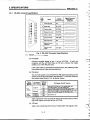
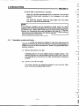
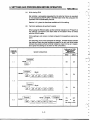
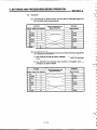
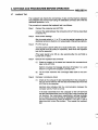
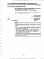
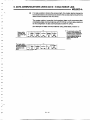
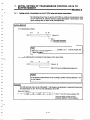
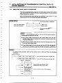
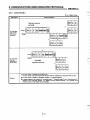
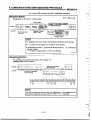
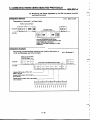
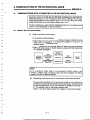
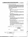
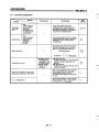
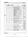
REVISIONS
?-
P
L
i
r
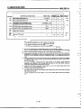
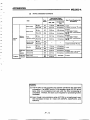
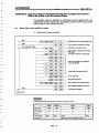
*The manual number is given on the bottom left of the back cover.
Print Date
Jan., 1992
*Manual Number
IB (NA) 66360-A
~
Revision
First edition
...--P
.
.
..
I
INTRODUCTION
--.51
!
Thank you for choosing the Mitsubishi MELSEC-ASeries of General Purpose Programmable
Controllers. Please read this manual carefully so that the equipment is used to its optimum.
A copy of this manual should be forwarded to the end User.
1
1
J
CONTENTS
1. GENERAL DESCRIPTION
.. ... . . .
-
1 10
.
.
....
. . . . . . . . . ... . . . .. . . . . . . .
. . . . . . . .. . . . . . . . . . . . . . . . . . . . .. . . . . .
. . . .. . .. . . . . ....
.. .
. ... . . . . . .. . . .
. . . . .. . ... ... . . . . . . .. . .. . ..
SYSTEM CONFIGURATIONS . . . . . . . . . ... .. ..... .... . .. ... .. ... .. . 2 - 1 2 - 21
2 1 Overall Configurations . . . . . . . . . . . . . . . . . . . . . . . . . . . . . . . . . . . . . . . . . . . . . . . . , . . 2 - 1
~~
2-2
2.2 A p p l i c a b l e S y s t ~ ~.....................................................
2.3 System Configurationsand Available Functions . . . . . . . . . . . . . . . . . . . . . . , . . . . , . . 2 - 4
23.1 1 : 1 ratio of an external device (computer) to a PCCPU . . . . . . . . . . . . . . . . . 2 - 4
23.2 1 : n ratio of an external device to PC CPUs . . . . . . . . . . . . . . . . . . . . . . . . , . . 2 - 7
23.3 2 : 1 ratioofextemaldevicestoaPCCPU .......... . ..............,. 2-10
Features
........................
.... ....................
1-4
1.1.1 Control operationsin data communications
. .. 1 -4
1.1.2 System configurationand the number of stations when a computer
.
. ., , , .
1 -7
link system is constructed
1.1.3 Link with a computer through datalink systems
. ... . .. .
1 -9
. ...
. . . . . . , , . 1 - 10
1.1.4 Modeswitchingfunction . . . . . . . . . . . .
. . . .
, .
. . . , 1 - 10
1.1.5 Transmission control function
1.1
2
. . . . . ... . . .. . ... . .. .. . . .. .. . . .. . .. . . . . . .. 1 - 1
-
,
2.3.4 2:nratioofextemaldevitoPCCPUs ............................
2.3.5 m:nratioofextemaldevicestoPCCPUs
........................
23.6 Links with an external device (such as a computer)
through datalink systems
.
.
. , , ,
2-13
...
2-16
. . . . . . . . . . . . . . . . . . . . . . . .. . . . . .. . . , . 2 - 19
3.1
3.2
3.3
3.4
3.5
. . . .. . . . . . . . . . . . . . . . . .. . . . . . . .. .
. . . . . . . . . . . . . . . . . . . . . . . . . . . . . . . . .. .
. . . . . . . . . . . . .. . . . ... .. . .. . .
... ... . . . . . . . . . .. . . . . . .
. . . . . . . . . . . . . . . . . . . . .. . . . .
. . . . ... . . . . .. .. . . . .. .. .. .
. . .. . . . . . . . . . . . . . . .. . . . . . . . . . .
. ...
. . . . . ...... . .
..
..
. .. . . . ..
. ..
.. .
.
. . . ..
.. . . . .. .
. . . . . ... .
..
. . . . . .. .
.. . . . . . . . . . . .
. . .. .... . . . ... . . . ..
. . . . . . . . . . . . . . . . -. . .
. . . . ... . . . . . . .... . .. .. .
. . . . . . . . . . . . .. . .
.
..
.
. .. . .. . ....
GeneralSpeCificati . .
..
... . . . . . . . . .
. 3-1
Perf~nnan~eSpeCificatiOns
..
.. .
.. ,..,, 3-2
3.2.1 Transmbsionspecifications.. . .
.... . .
..
. . 3-2
3.2.2 RS-232CCOnnectOrspecificati
..
. . . . ..
. . . . 3-3
3.2.3 RS422 terminal Mock specifiions
,
. . ..
, , 3-5
.
. .. , , , 3 - 5
3.2.4 RS422caMe~pecifications... . . . . .
Data Communications Functions
.
. , , . , . ., ,, . , 3 - 6
3.3.1 Functions availableusing dedicated protocots and commands .
., . . . , 3 - 6
, . . , .. . .,
, 3 - 13
3.3.2 Functions available in the no-protocol mode .
3.3.3 Functions available in the bidirectional mode . . . . , . , , , , , .
. , . 3 - 14
3.3.4 Transmission error data read function . . . . . . . . . . . , . , , . . , . . . . . . 3 - 15
M o d e Switching Function DuringA171C24 Operations
. . , , , , , , , . , 3 - 16
, . . , . . . . . . . . , . 3 - 16
3.4.1 Precautions whenmode switching . . . . . . . .
3 - 20
3.4.2 Procedure for switching themode from an external device . . . . . .
3.4.3 Procedure forswitching the mode from a PC CPU
. , , , , , . . 3 - 22
Data Communications Transmission Control Function . .
, . ,
3 - 24
3.5.1 Precautions when controllingtransmission
.
. . . . . . . 3 - 24
3.5.2 DTR /DSR (EWDR) control. . . . . . .
. . , . . . , , . . . 3 - 28
3.5.3 DCl/DC3 transmission control . .
. . . . . . . . . . . . . . , . 3 - 30
3.5.4 DCl/DC3 receive control . . . . . . . . . . . . . .
. . . . . . . . . . . . . . . , 3 - 31
3.5.5 DC2DC4sendcontrol ............................................
3-32
3.6
3.7
4
.
3.5.6 DC2/DC4receive contrd ..........................................3-32
I/OSignalsListfOfCPU ..................................................
3-33
BufferMemoryApplications and Allocation ..................................
3-36
SElllNGS AND PROCEDURES BEFORE OPERATION
4.1
4.2
4.3
4.4
4.5
..
'.-.
.
.................. 4 .1 .4 .21
Settings and Procedures M o r e Operah'on ..................................
4.
1
Nomenclature ..........................................................
4.
2
4.2.1 Nomenclature ....................................................
4-2
4.2.2 LED signals and displays ..........................................
4-3
Settings ...............................................................
4-5
4.3.1 Setting the dedicated protocol.no-protocol
or bidirectional mode
4-5
4.3.2 Setting of transmission specifiiions. main channels.
andterminalresistance ............................................
4-6
4.3.3 Stationnumbersetting
............................................ 4 - 9
Loadingandlnstallation .................................................
4-10
instructions ............................................
4-10
4.4.1 Handling
4.4.2 Installationenvironment ..........................................
4-10
Externalwiring ........................................................
4-11
4.5.1 Precautionsduringwiring .........................................4-11
4.5.2 Connectingthe RS-232C connectors ...............................
4-11
4.5.3 Connectingthe RS422 connectors
4-13
4.5.4 Connecting a muitidrop linkand setting modesand terminal resistance ... 4 - 14
Self-loopbackTest .....................................................
4-17
4.6.1 Proceduretocarryouttheself-loopbacktest .........................
4-17
4-19
4.6.2 Setf-loopback test operations ......................................
LWpbaCkTest ........................................................4 - 2 0
InspectionandMaintenance .............................................
4-21
mode.
...
.................................
4.6
4.7
4.8
5
.
HALF-DUPLEX COMMUNICATIONS USING THE R S - 2 3 X INTERFACE
5.1
5.2
5.3
5.4
.
6
System ConfigurationsandFunctions
Buffer Memory Settings
......................................
6.3
5.
1
..................................................
Wiring ................................................................
ON/OFF Timing of the CD and RS Signals of the AJ71C24 .....................
5.4.1 Datatransmissiontiming from an external device ......................
5.4.2 Data transmission timing from an A171C24 ...........................
DATA COMMUNICATIONS USING AN M : NMULTIDROPLINK
6.1
6.2
...... 5 .1 .5 .9
...........6 .1
5-2
5-3
5-4
5-5
5-7
6
.11
KeyPoints .............................................................. 6 - 1
ConditionsforComputerInterlock .......................................... 6 - 2
6-2
6.2.1 Computer station number allocation ...................................
6.2.2 Maximum data communications timeper computer ......................
6-3
6.2.3 Command and messageformat for data communications
amongcomputers .................................................
6-4
Procedure for Data Communications with a PC CPU ........................... 6 - 5
6.3.1 Communications between each computer and PC CPUs .................6 - 5
6.3.2 Data communications with PC CPUs by setting a master station and
slavestations .....................................................
6-8
b
p-'
..
.
/
..
. . . . .
.
c
.
-
.
i
.
7
F
b
.
L
...............................................
7.1
7.2
c
.
yr
7.3
c
.
7.4
P
I
ri
7.5
7.6
7.7
.
8
8.3
8.4
F
c
..
r
8.5
8.6
8.7
7
"a
7.2.1 Setti prioritv of transmissionto the A171 C24
using alfduplextransm'wsion .......................................
7.2.2 Setting non-priority oftransmissionto the A171C24
7-4
withthehdfdwttansmission .....................................
7-5
Reading TransmissionError Data ...........................................
7-7
7.3.1 Reading the error LED display status ..................................
7-7
7.3.2 Turning OFF error LEDs
7-8
Settings in the No-Pratocol M o d e ........................................... 7 - 9
7.4.1 Setting the m>-protocdmode receive-completedcode
7-9
(for receive withVariaMe-length data) ..................................
7.4.2 Specifying no-protocol receive completion datalength (fixed length) .......7 - 10
7.4.3 Settingawordorbyteunitintheno-protocolmode ..................... 7-11
send ......................
7 - 12
7.4.4 Setting a buffer memory area for no-protocol
7.4.5 Setting a M e r memory areafor no-protocol receive .................... 7 - 13
Settings in the BidirectionalMode ..........................................
7 - 14
ModeSwitchSetting .....................................................
7-17
7.6.1 Readinginthemodesettingstate ...................................
7-17
7.6.2 Mode switching designation .......................................
- 7- 18
Transmission Control Setting .............................................
- 7- 20
7.7.1 How to set transmission control .....................................
7 -. 20
7.7.2 Settingsfor changing theaddresses of DC1 to Dc4 codss ...............7 - 21
.............................................
COMMUNICATIONS USING DEDICATED PROTOCOLS
8.1
8.2
L
.1 .7 .21
setting Rs-232C CD Terminal Check Enable/Diile ........................... 7 - 2
Setting the TransmissionMethod for RS-232C .................................
7- 3
INITIAL SETnNG OF TRANSMISSION CONTROL DATA TO
BUFFER MEMORY
................8 .1 .8 .112
Data Flow in Communications with Dediied Protocols .......................
8.
1
ProgrammingHints ......................................................
8-2
8.21 To write data to thespecial use area in buffer memory .................. 8 - 2
8.22 PC CPU operation during data communications .......................
8- 3
8.23 Precautionsduringdatacommunications .............................
8- 4
Basics of DedicatedProtocolControlProcedures
............................ 8 - 5
BasicFormats of Dedicated Protocd .......................................
8-6
8.4.1 COWOIfOrmatl ..................................................
8-7
8-8
8.4.2 Control format2 ..................................................
8.4.3 Control format3 ..................................................
8-9
8.4.4 Control format4 .................................................
8 - 10
8.4.5 Setting protocol data .............................................
8- 11
Transmission SequenceTiming Charts and Communications Time ............. 8 - 16
Character Area Data Transmission ........................................
8 - 19
DeviceMemory Reamrite ..............................................
8 - 22
8.7.1 Commandsanddeviceranges ....................................
8-22
8.7.2 Batch read in units of bits .........................................
8 - 28
8.7.3 Batch read in units o
f words .......................................
8 - 30
8.7.4 Batch write in units of bits .........................................
8 - 34
__
..._
....
__......
.
.
.......................................
...................
8.8
8.7.5 Batchwriteinunitsofwords
8-36
8.7.6 Testingdevicememoryinunitsofbit(randomwrite)
8-40
8.7.7 Testingdevicememoryinunitsdwords(randomwrite) ................ 8-42
8.7.8 Monitoringdevicememory ........................................
8 - 44
Extension File Register Read and Write ....................................
8 53
8.8.1 ACPUcommon commands and addresses ..........................8 - 53
8.8.2 AnACPU dedicated commands and device numbers .................. 8 - 55
8.8.3 Precautions during extension file register read/write................... 8 - 58
8.8.4 Batch readof the extension file register (ACPUcommon command) ...... 8 - 59
8.8.5 Batch write of the extension file register (ACPU common command)
8 - 60
8.8.6 Direct readof the extension file register (AnACPU dedicated command) . . 8 - 61
8.8.7 Direct writeto the extension file register (AnACPUdedicated command) . . 8 - 62
8.8.8 Testing (random write) the extensionfile register
(ACPU common command) .......................................8 - 63
8.8.9 Monitoring the extension file register ................................
8 - 64
Buff& Memory Read and Write ...........................................
8 - 67
8.9.1 Commands and buffer memory ....................................
8 - 67
8.9.2 Reading data from buffer memocy (ACPU common command) .......... 8 - 68
8.9.3 Writing data to buffer memory (ACPU common command) ............. 8 - 69
Special Function Module Buffer Memory Readand Write .....................
8 - 70
8.1 0.Commands
1
and designation ......................................
8 - 70
8.10.2Special function module numbers usingcontrd protocols . . . . . . . . . . . . . . 8 - 72
8.10.3 Reading data fromthe special-function module buffer memory
(ACPU common command) .......................................
8 - 74
8.10.4Writing datato the special function module
buffer memory
(ACPU common command) .......................................
8 - 75
Remate Run/Stopof PCCPU and Reading PC CPU Model Name
8 - 76
8.11.1 Commands .....................................................
8-76
RUN/STOP ..............................................
8 - 77
8.1 1.Remote
2
8.1 1.
Reading
3
PC CPU model name .....................................
8 - 79
ProgramReadWrite ....................................................
8-80
8.1 2.
Precautions
1
during program reaWrite ..............................
8 - 80
8.12.2 Program read/write control procedures ..............................
8 - 81
8.12.3 Parameter memory read/write .....................................
8 - 83
8.1 2.Sequence
4
program read/write .....................................
8 - 87
8.1 2.Microcomputer
5
program read/write .................................
8 - 93
8.1 2Comment
.6
memroy read/write ......................................
I
8 - 97
8.12.7 Extension comment memory read/write ............................ 8 - lo0
GlobalFunction ......................................................
8-103
8-103
8.13.1 Commandsandcomrol .........................................
Setting
the globalfunction (ACPU common command) ............... 8 - 104
8.1 3.
2
Ondemand Function ..................................................
8 - 105
8.1 4.Ondemand
1
handshake signaland buffer memory ................... 8 - 105
8.14.2 Ondemand function control procedure ............................ 8 - 106
On-demand
function designation ..................................8 - 109
8.1 4.
3
LoopbackTest .......................................................
8-112
-
.....
8.9
8.10
8.11
8.12
8.13
8.14
8.15
..............
L.
nL
j '
L
b-.
P-
I
9.
J
1
r
-
L
c
c
L
.
c
1..
P
.-
r-
.r -
COMMUNICATIONS WlTH A COMPUTER IN THE NO-PROTOCOL MODE
9.1
9.2
9.3
9.4
9.5
9.6
.. 9 - 1
-
-
9 18
BasicsofthebPrdocdMode ...........................................
9-1
Handshakel/OSinals
9-2
ProgrammingHints
9-3
9.3.1 Towritedatatothespecialuseareainbuffermemory
9-3
9.3.2 Precautions during data communications ..............................9- 4
Basic Program to Readmrite Buffer Memory
9- 6
ReceivingDataintheN~ocolMode(ExtemalDevice-.AJ71C24) ........... 9-9
SendingDataintheNo-PratocdMode(A171C24~ExtwnalDevice)
9-15
..................................................
......................................................
....................
.................................
...........
10. COMMUNICATIONS IN THEBIDIRECTIONALMODE
.................10- 1
-
10 26
10-2
10.1 BidirectionalModeBasics ...............................................
10 - 4
10.2 Handshake Si- and Buffer Memory ....................................
ProgrammingHints
......................................................
10-8
10.3
10.3.1 System configurationand commuflications mode for bidirectional
modecommunications ...........................................
10-8
10.3.2 Towritedatatoaspecialappkatiiareainbuffermemory ........... 10-9
10.3.3 Precautions during data communications ...........................
10- 10
10.4 Bidirectiod Control Procedure Basics ...................................10- 12
10.5 BidirectionalCommunicatii Basics .....................................
10- 13
10-13
10.5.1 COntrd~dOCQk ...............................................
10.5.2 Messageformat ................................................10-14
10.6 Processing an A171 C24
for Simuttarmus Send in FulCDuplex Mode .......... 10- 17
10- 18
10.7 Basic Programto ReadMlrite Buffer Memory ...............................
10.8 Receiving Data in the BidirectionalMode (Computer + A171 C24)
............. 10- 20
10.9 Transmitting Datain the BidirectionalMode (A171 C24
-. Computer) ........... 10 - 23
11. TROUBLESHOOTING
...........................................
1 1 - 1 -11-9
11.1 NAKErrorCodeswithDedicatedProtocds ................................. 11 - 1
11.2 BidirectionalModeErrorCodes .......................................... 11 -3
11.3 TrouMeshoatingOFF ...................................................11-4
11.3.1 TrouMeshootingflowchart ........................................
11-4
11.3.2 Whenthe'RUN'LEDistumedOFF ................................
11-5
11.3.3 Whentheneutralstatedoesnotchangeordataisnatreceived ......... 1 1 -6
11.3.4 Whenthe2-C/N(LEDNo.16)or4-CM(LEDNo.20)istumedON ....... 11-7
11.3.5 Whencommunicatiisometimesfails .............................
1 1 -8
11.3.6 Whenundecodeddataistransmitted ...............................
1 1 -9
APPENDICES
APPENDIX 1
1.1
1.2
1.3
r
..................................................
APP-1
Precautions Concerning Compatibility and the Use of
Exs
i tn
i g Programs Prepared forthe AJ71C24 Computer Link Module
-
APP-27
...... APP - 1
Compatibility .........................................................
APP-1
Precautions when Using ExistingPrograms ...............................
APP - 1
Function Comparison .................................................
APP-2
APPENDIX 2
Precarrtkns concerning Compatibility and the Use d Existing
Programs Prepared forthe A171C24S3 Computer Link Module.......... APP - 4
2.1
Compatibility
.........................................................
2.2 Precautions When Using ExistingPrograms
2.3 FunctionComparison
APP-4
...............................APP - 4
..................................................APP-5
APPENDIX 3 Precautions Concerning
C o m p a t i b i l i t y and the Use of Existing
Programs Prepared for
the AJ71C24S6 Computer Link Module
3.1
3.2
3.3
.......... APP - 6
Compatibility .........................................................
APP - 6
PrecautionsWhen Using ExistingPrograms ...............................
APP - 6
APPENDIX 4
..................................................
ASCIICode Table ................................................
APPENDIX 5
Communications Time between aPCCPU and an A171C24
APPENDIX 6
Precautions During CommunicationsWhen Using 2
2
APPENDIX 7
S p e d Function Module Buffer Memory Addresses
APPENDIX 8
Sequence Program Example Showing H o w to Output
Word Device Datato the Printerin the No-ProtocolMode
APPENDIX 9
Example of a Sequence Program for Data Communications
in the Bidirectional Mode
..........................................
APP - 21
...................................................
APP - 24
APPENDIX 1 1 A171 C24Setting Record Form .....................................
APP - 25
Function Comp'son
APP - 6
APP - 7
.............APP - 8
Interface
...... APP - 11
...................APP - 13
............... APP - 18
8.1 WhenOtherThanAnACPUisUsed .....................................
APP-18
8.2When the AnACPU is Used ............................................
APP -20
APPENDIX 10ExternalView
-vi
-
L
I
c
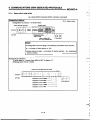
1. GENERAL DESCRIPTION
MELSEC-A
f-
- 1
'
GENERAL DESCRIPTION
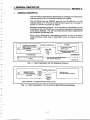
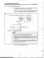
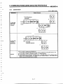
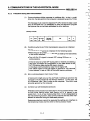
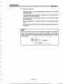
1.
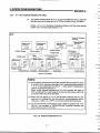
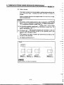
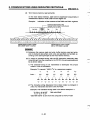
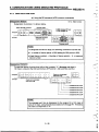
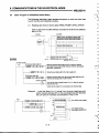
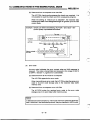
This User's Manual describes the specifications, handling andtransmission
control protocols of the AJ71C24-S8 computer link module.
The AJ71C24-58 has one RS-232C port and one RS-422 port. It is the
interface between a PC CPU and an external device (such as a computer or
printer) or to theCPU of another PC station.
Dedicated transmission protocols 1 to 4 are used as transmission control
procedures on the AJ71C24-S8 and a no-protocol mode anda bidirectional
mode are also available. The user can select and set these independently
for the RS-232C and RS-422 ports.
When using a dedicated transmission protocol or the no-protocol
mode/bidirectional mode, data is transmitted using the codes as shown
below.
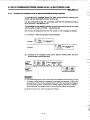
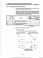
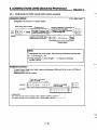
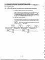
~
PC
CPU
.
FlS232C or Rs-422
Computer
cable
Autome communications
sequence prqm
'
AJ71
ENDpmemsing.
C24
code ASCII
BIN code
Read
earths
.
\
Trammitwd.ta
\
\
Write
\
data
\
(ASCII code)
Transmitted data
Transmitted
-
~AnlC24mmeftsdatabetween
BIN code andA S C I I code.)
(1234~)
Fig. 1.1 Data Transmission with the Dedicated Protocol
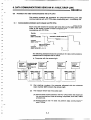
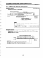
r
PC
CPU
.
Sequence program
TOFROM
inetwctions
Oon to FFH
.
Rs232C or 2
2
cable
BUnW
m e w '
AJ71
C24
T
Oac to FFH
External device
(such as a computer, printer)
Transmit
Receive
I
(Data is transmitled in unchangedcode through the buffer memory.)
Fig. 1.2. Data Transmission in the No-Protocol Mode/Bldirectional
Mode
I
1-1
1. GENERAL DESCRIPTION
MELSEC-A
Compared with the AJ71 C24-S3 and AJ71 C24-S6 computer link modules,
the AJ71C24-S8 supports the followingsix additional functions:
[(l)
to (6) are the additional functions when compared with the
AJ71 C24-S3]
(1)
Commands dedicated for use with the A2ACPU(Sl) and A3ACPU:
c
All memory devices of the A2ACPU(S1) and A3ACPU (the AnACPU in
this manual) are accessible using these dedicated commands.
(2) Data transmission in the bidirectional mode:
This feature allows the AJ71 C24-S8to interface 1:ldata communications using the ACK code between a PC CPU and a computer.
When data is transmittedfrom the AJ71 C24-S8to a computer, a control
code ENQ, the data length code, and a check sum are added respectively to the beginning, the middle, and the end of the send message.
(The check sum is optional.)
c
When the AJ71C24-S8 receives data from a computer, it transmits a
control codeACWNAK back to thecomputer. This indicates the result
of the receive (normal/abnormal).
The AJ71 C24-S8 thus adds theENQ code, data length, and check sum
and checks the reception of the response message at the data transmission. It checks the received data andsends the response message
after it received data.
Ir
The length of a data communications sequence program can be shortened by using the bidirectional mode.
(3) The communications mode using the RS-232C interface can be set to
either full-duplex or half-duplex:
The communications mode using the RS-232C interface
of the
AJ71C24-S8 can beswitched either to full-duplex or half-duplex according to thespecifications of the peripheral device.
(4) Multidrop link with more than one computer is possible:
More than one computer can be put into a multidrop link with the
AJ71 C24-S8.
The PC CPU modules in the multidrop link can be accessed from the
computers for read/write of device data and sequence programs.
1-2
c
L
1. GENERAL DESCRIPTION
,
L.
MELSEC-A
,
1(5) and (6) are the additional functions when compared with the
AJ71C24=S6]
( 5 ) Mode switching function when the AJ71C2448 operates
The AJ71C24-S8's RS-232C/RS-422interface canbe switched between
the following modes after a start-up:
N+pratocol mode
.
.
Bidirectional mode
(6) Transmission control function using DCl/DC3 and DC2/DC4
Data communications between the AJ71 C24and an external device can
be controlled by using the DCl/DC3 and DC2/DC4 codes.
DCl/DC3 send control, DCl/DC3 receive control: Enables or disables
data send andreceive.
DC2/DC4 send control, DC2/DC4 receive control: Controls the
range of sendheceive data.
valid
tf any exirting program are ured with the AJ71C24-S8, reo Appendix 1.2.3 for interchangeability between the AJ71 C24-S8 and the following devicer.
0
AJ71 C24 computer link modules
0
AJ71 C2CS3 computer link modules
0
AJ71 C24-S6 computer link moduler
P
t -
c
L
..
P
..-,
t'--''
f
r
\
1-3
1. GENERAL DESCRIPTION
1.1
MELSEC-A
Features
The features of the AJ71C24-S8 computer link module (hereafter called the
AJ71C24 in this manual) are given below.
1.1.1
Control operations In data communications
Data transmission operations between an AJ71 C24and external devices (e,
g., computers) can be controlled using either the dedicated protocols (*1)
or in the no-protocol/bidirectional mode. These control operations can be
selected individually with the RS-232C and RS-422 ports of an AJ71C24.
(1) Communications using the dedicated protocols
Communications at the request of the computer
Data communications is always initiated by the computer.
Designated data is transmitted accordingto the request command
transmitted from a computer to an AJ71C24.
It is not necessary to create and change special sequence
programs in order to use an AJ71C24.
Read and write possible to andfrom all PC CPU devices
Data can be read from all PC CPU devices. This permits observation and monitoring of all operations, as well as the collection
and analysis of data. Data can bewritten to all PC CPU devices.
This permits production control and production directives to be
carried out.
An AJ71C24 can uploadand download programs from aPC CPU.
PC CPU programs (main sequence and subsequence control
programs and microcomputer programs), parameter data and
comment data are read by the computer and stored. When
required they can be written to the PCCPU to changethe
program.
Remote RUN and STOP control of the PC CPU
The PCCPU can be remote-controlled by means of RUN and
STOP instructions from the computer.
When multiple computers and PC CPU modules are connected
to a link with an AJ71C24 module, the input (X) signals of the
CPUs in the link can be turned ON/OFF using any computer in
the link. This function can immediately stop or simultaneously
start all CPUs in the link.
(This function is called the globalfunction of the AJ71C24.)
-*i
Communications at the request of the PC CPU
The PC CPU transmits the data send request.
When the emergency data needs to be transmitted from aPC CPU
to a computer, the PC CPU transmits a send request to theAJ71C24
to make the computer execute an interrupt processing.
:9
'h
+.J
'..
1-4
a
Y
F
!
i
(This is theon-demand function of the AJ71 C24. It is availabte
only when one computer is connected to one PC CPU.)
'1
r-
* 1:The dedicated protocols consist of four different protocols.
The term 'dedicated protocols' used in this manual is the collective term for these protocols.
(2) Communications in the no-protocoVbidirectiona1modes
Either the no-protocol mode or the bidirectional modecan be set.
(a) Communications in the no-protocol mode
1) Data communications can be initiated by a PC CPU
Data communications can be initiated by a computer or any PC
CPU. Data can be transmitted from a PCCPU to an external
device by using the TO instruction in the sequence program to
write data tothe buffer memory.
Data transmitted from an external device can be read by a PC
CPU using the FROM instruction in the sequence program.
The following example shows a system with a printer, CRT and
keyboard terminal connected in a 1 :1 ratio. Data can be output
from the buffer memory to the printer or a CRT display using the
TO instruction. Data input from thekeyboardtothe
buffer
instruction fromthe PC CPU.
memory can be read using FROM
a
r
- -
PC CPU
c
t
L
TO instruction
(write) (Send)
Printer, CRT, computer
AJ71 C24
FROM iMtruction
(F-Q
Computer, keyboard
2) Receiving data length can be set to variable or fixed:
?I
L
-
1
P
c
.
.
The Length of the data transmitted from an external device and
received by the PC CPU can be set to variable or fixed.
i) Receiving variable-length data:
Data receive stops when the receive completed code set by
the user is received.
ii) Receiving fixed-length data:
Data receive stops when the fixed length of data set by the
user is received.
Both the receive completed code and the receive-completion
data length can be freely set by the user.
3) Variable communications memory area
The user memory area can be allocated to suit the purpose and
application of the data transmission.
1, GENERAL DESCRIPTION
MELSEC-A
(b) Bidirectional communications
1) Data communications can be initiated by a PC CPU
Data communications can be initiated by a computer or any PC
CPU. Data can be transmitted from a PCCPU to an external
device by using the TO instruction in the sequence program to
write data to the buffer memory.
The data send operation is completed when the response message to the sent (received) data is received from the computer.
The result of the send (normal end/error) is stored in the buffer
memory and can be read out.
The data received from the computer can be read withthe FROM
instruction of the sequence program.
(When data is transmitted by an AJ71C24)
Data
TO instruction
Xno ON
PC CPU
-
(Send complasd)
FROM instruction
send
AJ71 C24
Reapomereceke
Computer
(Send result)
2) Data length is set within the send message
Data. length is set within the send message when the data is
transmitted to a device.
The receiving side recognizes the data length by the send message.
Data
I
I
1
-pq
check
I
I
I
T
The send data of the AJ71 C24is processed as follows.
ENQ:.....................
Data length:
Added to the head.
........The rend data length set in the buffermemory is transmitted,
Data:.....................
The send data stored in the buffer memoryir transmitted.
Sum check: .........Computed with the sum checking range ina message.
The data transmittedby a computer and receivedby an AJ71 C24
is processed as follows.
ENQ:.....................
Data length:
Data:
Checked and removed fromthe received data.
........Stored in the buffer memory as the received data length.
...........
Stored in the buffer memory as the received data.
Sum check: .........Checked and removed fromthe received data.
3) Variable communications memory area
The user memoryarea can be allocatedto suit the purposes and
applications of the data transmission.
1-6
1. GENERAL DESCRIPTION
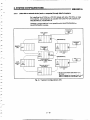
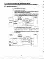
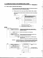
1.1.2
MELSEC-A
System configurrtion and the number of daions when a computer link system is constructed
A computer link system using the dedicated protocol, no-protocol
mode, or
bidirectional mode can be constructed by connecting the computer to the
PC CPU in the ratios of 1 :1, l:n, 2:1, 2:n, and m:n. (*1)
When the connection ratio is l:n or 2:n, up to 32 PCCPU stations can be
tied toone link system.
When the connection ratio is m:n, up to 32 stations of computers and PC
CPU modules can be tied toone link system.
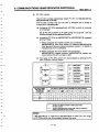
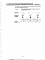
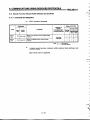
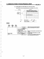
1) When the connection ratio
module is 1:n:
of the computer to the PCCPU
This method of linking uses one computer and multiple PC CPU
modules for up to 32 stations.
Data communications is executed between the computer and
designated PC CPU stations.
This link system is called a multidrop link system.
I
AJ7lc24
(Mi0)
&
A n 1 c24 (stati&2)
Max. 32 stations (Number of PC CPU stations)
1-7
.. .
.. ..
r---
A n 1 C24 (strrtio/n 31)
-
a
i
u
1. GENERAL DESCRIPTION
MELSEC-A
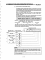
2) When the connection ratio of the computer
module is m:n:
to the PCCPU
This method of linking uses more than one computers and multiple PC CPU modules for up to 32 stations.
Data communications is executed between a computer (which
has acquired theaccess right through the communications with
other computers) and designated PC CPU stations.
This system is also called a multidrop link system.
w
n
q
~ - p ~ # ' l ~ J J
C
cP
C
P
U
U
U
A n 1 C24 (Station 0)
A n 1 C24 (Station 1)
A n 1 C24 (Station 2)
_--
c
P
A n 1 C24 ( W o n 24)
Max. 32 stations (Number of PC CPU stations)
1:The on-demand function and the data communications in the
bidirectional mode mentioned respectively in Section 1.1.1
(l)(b) and (2)(b) cannot be used with the multidrop link sys-
tems.
'B
1
I
Y
1-8
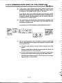
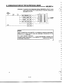
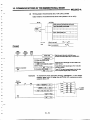
1, GENERAL DESCRIPTION
,,...
,
MELSEC-A
~
Unk with a computer through data link systems
1.1.3
In a system connected through the following data link system, if the system
contains a PCCPU connected to a computer via an AJ71C24, data communications is possible between the computer and a PC CPU not equipped
with the AJ71 C24.
However, communications is not possible with
AOJ2P25/R25 modules.
(1)
AOJ2CPUP23/R23or
PCCPU in the MELSECNET (It)
0
0
Master/Local stations:
Can communicate all data (device memory, programs, etc.).
Remote I/O station:
Can communicate only special-function module’s buffer data.
(2) PCCPU in the MELSECNET/B
0
Master/Local stations:
Can communicate all data (device memory, programs, etc.).
When a computer is connected to
a local station:
(Twc-tjer s y s t e m )
I
c-
L..
..-
1
M
: Masterstation
:Localaation
: Remote Vo station
U m : Local /master station
:for the third tier
I
:Thir&ierMrtatior
L
R
When a computer is connected to
0
St.bionthatcan
autd/mcmm d&a
a master station for the third tie:
n
When a computer is connectedto
a third-tier local station:
(Three-tier system)
@-@J
c
c
P
-,.
The stationthat can send/mceive data does ne4 v q even if the aecond tier uses a MELSECNETB
and the third tier uses a MELSECNET (11).
1-9
1. GENERAL DESCRIPTION
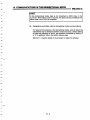
1.1.4
MELSEC-A
Mode switching function
After the AJ71C24 has started operating, the AJ71C24's RS-232C/RS422
interfaces can be switchedto another mode.
bprotocd mode
W e e n formats 1 to 4
1.1.5
Bidirectionalmode
Transmission control function
c
Data communications between the AJ71C24 and an external device can be
controlled by using DC codes or DTR/DSR signals.
I
(1) Control using DCl/DC3 or DC2/DC4 codes
*This function can be used for controlling data communications with
an external device connected to theAJ71C24 at the RS-232C/RS-422
interface.
il
e DCl/DC3 control refers to using theDC1 and DC3 codes to notify the
communicating device of the enabled/disabled state of data receive.
e DC2/DC4 control refers to using DC2 and DC4 codes to indicate the
valid range of sendheceive data.
4
e Data to besent/received must begin withDC2 code and end
with DC4
code.
r
I D c 2
Data
Dc4
(2) Controlusing DTR/DSR signals
c
*This function can be used for data communications with an external
device connected to the AJ71 C24at the RS-232C interface.
eDTR/DSR control refers to using the DTR and DSR signals to notify
thecommunicatingdevice
of the enabled/disabled state of data
receive of the AJ71 C24 orexternal device.
L
*The AJ71 C24controls the DTR signal as follows:
When data can be received: Turns ON the DTR signal.
When data cannot be received: Turns OFF the DTR signal.
L
*The AJ71 C24controls the DSR signal as follows:
When the DSR signal is ON: Sends when send data exists.
L
When the DSR signal is OFF: Sends only if the DSR is ON when send
data exists.
x
1-10
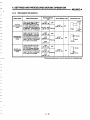
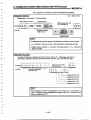
2. SYSTEM CONFIGURATIONS
2.
MELSEC-A
SYSTEM
CONFIGURATIONS
This section describes system configurations which can be combined with
the AJ71 C24.
2.1
OverallConfigurations
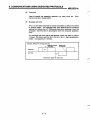
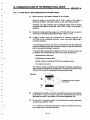
Fig.2.1shows the overall configuration of the A series system which is
loaded with theAJ71C24.
c.
c
External device
(such as a computer,
printer, CRT, etc.)
1
J
Type
r
L
1.
Building-type
PC CPU modules
'
1 1
Type
Main base units
AJ71 C24-S8
.-
I
+
r
L
~
AC30B
Exten 'on cables
(1) When loading the AJ7lC24 into
type A55B or A586 extension
base unit, see Section2.2 'Applicable System".
L .
~~
ACOGB
AClPB
Type
c
f
m
Computer link module
~OINTS
1
A32 B
A35B
A38B
1
-
II
(2) An extension base unit cannot
be connected to a type A328
main base unit (because an extension
connector
is not
provided).
c
"=----A!
1 I
Type
A680
A55B
A58B
Extension base units
-
,/"-
r.
Fig. 2.1 A Series System Overall Configuration
c
P
2-1
.
.
.
..
-
2. SYSTEM CONFIGURATIONS
2.2
MELSEC-A
.."
ApplicableSystems
The AJ71C24 can only be used in the systems described below.
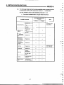
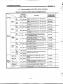
(1) Applicable PC CPU modules and the number of AJ71C24 modules
The table below shows the PC CPU modules to which the AJ71C24 is
applicable and the number of AJ71C24 modules which can be connected to the PC CPU modules.
The PC CPU modules listed below include those which have the MELSECNET link function.
(e.g., AlCPU includes A1 CPUP21/R21 to which an AJ7lC24 can be
connected.)
PC CPU Modules
Number of
Connectable
AJ71 C24s
Notes
If the following modules are used with the
AJ71C24, the maximum number of connectable AJ7lC24 modules cannot exceed 2 or
6. (See previous column).
AW2H
Al, AIN
A1S
A2(-S1),A2N(-S1)
AS, A3N
A3H,A3M
A73
0
AD51 (S3)/AD51 HIntelligent Communication Module
0
AD570 Graphic controller Module
2
AJ71C21 (Sl) Terminal Interface Module
A2A(-S1)
A3A
6
0
AJ71C22(Sl) Mukidlop Link System
Module
0
AJ71C23 Higher Controller High Speed
Link Module
0
AJ71C24(S3/S6) Computer Link Module
0
AJ71 E71 Ethernet Interface Module
cl
;-1
f
4
(AOJOCPU and A2CCPU are not applicable.)
(2) Applicable base unit
The AJ71C24 can be inserted into
any slot of a main base unit or
extension base unit with these two exceptions:
(a) The power supply capacity may be insufficientto load theAJ71C24
into an extension base unit with no built-in power supply (A55B or
A58B). Wherever possible, avoid loading an AJ71 C24module into
this typeof extension base unit. If it is necessary to use an AJ71C24
module in an extension base unit withno built-inpower supply, it is
important to consider (a) the power supply capacity of the main
base unit, and (b) the voltage drop along
the extension cables when
selecting the extension cables.
L
(b) (The User's Manual of the respective CPU module employed gives
details.)
2-2
w
c
2. SYSTEM CONFIGURATIONS
MELSEC-A
(c) The AJ71C24 should not be loaded into the last slot of the A3CPU
extension level 7.
L
.
.
tL...
P-
....
POINTS I
I
(1) The AJ71C24 can also be loadedinto the A81 CPUbase unit (A78B).
The A81CPU User's Manual givesthe commands available when the
AJ71C24 is loaded.
(2) The AJ71C24 cannot be used in a remoto I/O station.
2-3
2. SYSTEM CONFIGURATIONS
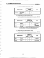
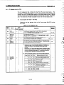
2.3
d
MELSEC-A
I
SystemConfigurationsandAvailableFunction*
The AJ71C24 is a link module to connect an external device (such as a
computer) and aPC CPU. The system can consist of a single external device
and from 1 to 32 PC CPU stations (1 : 1 to 32 ratio system) or two external
devices and from 1 to 32 PC CPU stations (2 : 1 to 32 ratio system). The
connection may be made in two ways: using the RS-232C port or the RS-422
port.
2.3.1
d
-.
1 : 1 ratio of an external device (computer) to a PC CPU
3
1
(1) The system configuration for a 1 : 1 ratio of an external device (such as
a computer) to a PC CPU is shown in Fig. 2.2 below.
(Mode: [ ] - [ 1) in the figureindicates the range of setting set with the
mode setting switch of an AJ71C24 (see Section 4.3.1).
.1(
External device
(such as a computer,
(Mode: 1 to 8)
Computer link module
AJ71 C24
?,
To ex?
POINTS
' 1
I
U
(1) Use of the RS-232C and the RS-422 interfaces differs in that the
RS-422 is used to connect longdistances (up to 500 m (1640.5 ft))
and the RS-232C is used to connect short distances (a maximum of
15 m (49.2 ft)).
(2) To have the RS-232C communicate over a distance greater than 15
m (49.2 ft), use a modem or RS-232C/RS-422 converter between the
external device and theAJ71 C24.
3
Fig. 2.2 System Configurations (I)
4
I
2-4
(
2. SYSTEM CONFIGURATIONS
MELSEC-A
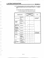
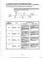
(2) The following tables list the
functions available when an external device
is linked with a PC CPU module to make a 1 : 1 configuration.
(a) The interface used to set dedicated protocols 1 to 4:
1) Functions available when using an external device
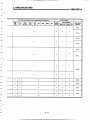
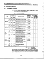
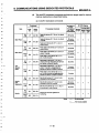
Intwtmss tor Ded1cat.d
Protocol
AV8Ii8bh Functions
us422
Not.
RS-232C
Aeadhvrite
I
Extension file
regists
Monitor
I
I
I
I
I
I
Readhvrite
I
I
Monitor
I
Buffer memory
I
AJ71 C24 of the
Fbadhvrite
Specid fun*
tion module’s
buffer memory
Readlwrite
Sequence1
Microcomputer
program
Readlwrite
0
Readhvrite
I o
self
Comment
I
Parameter
PC CPU
Global
Readlwrite
1
r
Remote
RUNISTOP
PC CPU type
read
Input signal (X)
ONIOFF
0
0
0
I o I o I
I o
Transmission
of received data
2-5
I
I
0
~
Self-loopback
I
0
I
I
test
0
Including extension devices
~
0
~~
0
Including extension comments
2. SYSTEM CONFIGURATIONS
Y
MELSEC-A
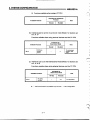
2) Functions available when using a PC CPU
Intorfaw8 for Dodicalod
Protocol
Availablo Functions
On-domand
Data transmisrion toexternal
devices
US422
RS-232C
0
0
Not.
-
(b) Interfaces used to set the no-protocol mode
Functions available when using an external device and a PC CPU
1
Available Functions
RS-232C
RS-422
PC CPU to
external device
I
Receive
,
External device
to PC CPU
,
inlerfacer for
No-protocol Mode
1
I
I o I o
1
I
Nolo
To computers,
printers, and
CRTs.
From computers
and keyboards
(c) Interfaces used to set the bidirectional mode
Availablo Funclions
I
'd
i
Functions available when using an external device and a PC CPU
I n t n t a c o s for
BidiroctionalModo
I
,?
J
'L
kJ
Note
RS-422
US-232C
Send
PC CPU to
computer
0
0
To computer8
Receive
Computer to
PC CPU
0
0
From computers
,a
I
19
I
d
2-6
a
2. SYSTEM CONFIGURATIONS
>
2.3.2
MELSEC-A
.
1 : n ratio of l
extemal dmflce to PC CPUs
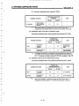
(1) The system configurations for a 1 : n (up to 32 stations) ratio of an
external device (such as a computer) to PC CPUS are shown in Fig. 2.3
below.
(Mode: [ ] to [ 1) in the figure the range of setting set with the mode
setting switch of an AJ71 C24 (see Section 4.3.1).
[System configuration 11
The external device is connected to the AJ71C24 modules using
the RS-232C
dovice
(computer)
Rspx interface
___--
RE422 interface
R5422cable
RE422 interface
RE422mbk
R5422 interface
Maximum of 32 stations
[System configuration 21
The external device is connected to the AJ71 C24 modules using
the RS-422
link modules
Computer
E 4 2 2 intedace
I
~OINTS
(1) When the mode setting is 5 to 8 , the RS-232C interface which is not
used for the multidrop link can be used for communications with a
computer, a printer, or a CRT in a no-protocol/bidirectional mode.
(2) Use of the RS-232C and the RS-422 interfaces differs in that the
R S 4 2 2 is used to connect long distances (up to 500 m (1640.5 ft))
and theRS-232C is used to connect short distances (upto maximum
of 15 m (49.2 ft)).
(3)To have the RS-232C communicate over a distance greater than 15
m (49.2 ft), use a modem or RS-232C/RS-422 converter between the
external device and theAJ71 C24.
Fig. 2.3 System Configurations (11)
2-7
2. SYSTEM CONFIGURATIONS
MELSEC-A
(2) The following tables list the functions available when an external device
is linked with the PC CPU modules to make a 1 : n configuration.
(a) The interface used to set dedicated protocols 1 to 4:
1) Functions available when using an external device
1
I
Available Functions
I Read/write
Device memory
Test
I
I
RS-422
0
Monitor
Readlwrite
Extension file
register
Test
0
Monitor
Buffer memory
AJ7lC24 of the
self
Readlwrite
Special function module's
Readlwrite
buffer memory
,
Inlerfacer ior Dadlcated
Prolocd
0
0
RS-232C
1
Note
I
0
Including extension devices
0
Including extension comments
4
Sequence/
~
Comment
Readlwrite
Parameter
Readlwrite
0
Remote
RUNISTOP
0
PC CPU type
read
0
PC CPU
Global
Input signal (X)
ON/OFF
Self-loopback
test
Transmission
of received data
2-8
1
'4
0
rc
0
I
c
.
2. SYSTEM CONFIGURATIONS
..
MELSEC-A
c
1
-
2) Functions available when using a PC CPU
4
P-
Intorfacor for I k d l m t o d
L
Protoeol
Arallablo Function8
?-
Data trawmirsion to external
devices
On-demand
c
Note
RS-422
RS-232C
X
X
-
(b) Interfaces used toset the no-protocol mode
Functions available when using an external device and aPC CPU
I
c.
I
P
I
F
Intortaco8 for
No-protocol Mode
Avaikblo Function8
I
Send
PC CPU to
external device
Receive
External device
to PC CPU
1
RS-422
1
RS-232C
I
I o
Note
I
To computers,
printers, and
CRTs.
From computers
and keyboards
~~
1 : If the external device is capable of performing full-duplex transmiasion,
.-.
data communications in the no-protocol mode can be performed.
c
(c) Interfaces usedto set the bidirectional mode
r
Functions availablewhen using an external device and aPC CPU.
c-
r
i
Avallablo Funcilons
L-
r
-
L.
I
I
Inlortaco8 f o r
Bidlrutional Modo
RS-422
I
Send
Receive
PC CPU to
computer
Computer to
CPU PC
2-9
Not.
RS-232C
I x l x I
I
l x I x
To computers
computerr
From
2. SYSTEM CONFIGURATIONS
2.3.3
MELSEC-A
2 : 1 ratio of external devices to 8 PC CPU
(1) The system configuration for a 2 : 1 ratio of external devices (such as
a computer) to a PC CPU is shown in Fig. 2.4 below.
(Mode: [ ] to [ I) in the figure indicates the range
of setting designated
with the mode setting switch of an AJ71C24 (see Section 4.3.1).
1-
Y
a
(A combination of two systems each of which has a 1 : 1 configuration.)
mm
External device
(such as a corn
puter, printer, CAT)
External d e v i i
(such as a corn
puter, printer,CRT)
AJ71 C24
POINTS
I
(1) One of the two interfaces is set to a dedicated protocol 1, 2, 3, or 4.
The other is set to a no-protocol/bidirectional mode.
i
(2) The use of the RS-232C and the RS-422 interfaces differs in that the
RS-422 is used to connect long distances (up to 500 m (1640.5 ft))
and theRS-232C is used to connect short distances (maximum of 15
m (49.2 ft)).
I
(3) To have the RS-232C communicate over a distance greater than 15
m (49.2 ft), use a modem or RS-232C/RS-422 converter between the
external device and theAJ71C24.
c
c
Fig. 2.4 System Configurations (Ill)
I
L
L
2 - 10
2. SYSTEM CONFIGURATIONS
MELSEC-A
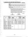
(2) The followingtableslist
thefunctions available when theexternal
devices are linked with the PC CPU modules to make a 2 : 1 configuration.
L.
..
(a) The interface used to set dedicated protocols 1 to 4:
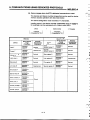
1) Functions available when using external devices
Available Fundionr
intorlacor for Dedicatod
Protocol
Note
Readlwrite
Including extension devices
Monitor
l o
Readlwrite
Extension file
register
Monitor
e
Buffer memory
c-
I
Readlwrite
Sequence
microcomputer
program
Readlwrite
0
0
Comment
Readlwrite
0
0
Parameter
Readlwrite
~~
n
c
r
PC CPU
I
1
I
Remote
RUNISTOP
PC CPU type
read
Global
Input signal (X)
ONIOFF
Self-loopback
test
Transmission
of received data
C
c
l o l o
Special function module's
buffer memory
2-11
I o
I o I o
0
0
0
0
Including extension comments
2. SYSTEM CONFIGURATIONS
MELSEC-A
e
2) Functions available when using a PC CPU
Intertacos for DodIca1.d
Protocol
Available Functions
Data tranrmisrion to external
devicer
On-demand
RS-422
RS-232C
0
0
Note
-
(b) Interfaces used to set the no-protocol mode
Functions available when using external devices and a PC CPU
I
I
I
Interfaces for
No-protocol Mode
Availablo Functions
I
Send
PC CPU to
external device
Receive
External device
to PC CPU
1
RS-422
I
RS-232C
I
I o I o
Not.
I
To computers,
printers, and
CRTr.
From computers
and keyboards
Functions available when using external devices and a PC CPU
Intortacos for
B l d l r o c l i o ~ Modo
l
Avalirble Funcllons
RS-422
I
Send
PC CPU to
computer
Receive
Computer to
PC CPU
I
2- 12
N ole
RS-232C
I o
1
I
o
I
o
'-
-
1
d
I
I
J
,/--
(c) Interfaces used to set the bidirectional mode
b
i
I
To computer8
computers
From
I
2. SYSTEM CONFIGURATIONS
2.3.4
2 : n rrtlo
to PC kPu8
external
(1)
MELSEC-A
The system configuration for a 2 : n (up to 32 stations) ratio of external
devices (such as a computer) to PC CPUs is shown in Fig. 2.5 below.
(Mode: [ ] to [ I) in the figure indicates therange of setting set with the
mode setting switch of an AJ7lC24 (see Section 4.3.1).
(A combination of two systems one of which has a 1 : 1 configuration and the otherhas a
i : n configuration.)
'OINTS
I
(1) One of the two interfaces of the AJ71C24 which is connected to the
external devices is set to a dedicated protocols 1, 2, 3, or 4. The
other is set to a no-protocol/bidirectional mode.
(2) When the mode setting is 5 to 8, the RS-232C interface which is not
used for the multidrop link can be used for communications with a
computer, a printer, or a CRT in a no-protocol/bidirectional mode.
(3) To have the RS-232C communicate over a distance greater than 15
m (49.2 ft),use a modem or RS-232C/RS-422 converter between the
external device and theAJ71 C24.
Fig. 2.5 System Conflguratlons ( I V )
2-13
2. SYSTEM CONFIGURATIONS
MELSEC-A
(a) The interface used to set dedicated protocols 1 to 4:
1) Functions available when using external devices
Inlorfacer for Dodkated
Protocol
Available Functions
RS-422
RS-232C
Read/write
0
0
Test
0
0
Monitor
0
0
Readlwrite
0
0
Test
0
0
Monitor
0
0
Buffer memory
AJ71C24 of the
self
Read/write
0
0
Special function module's
buffer memory
Read/write
0
0
Sequence/
microcomputer
program
Readlwrite
0
0
Device memory
Extension file
register
Comment
Including extension devices
'
1
Parameter
PC CPU
Not.
I
Read/write
l
o
l
o
Read/write
0
0
Remote
RUNlSTOP
0
0
Input signal (X)
ONlOFF
Self-loopback
test
Transmission
of received data
2- 14
l
I
I
PC CPU type
read
Global
-
0
0
Including extension comments
2. SYSTEM CONFIGURATIONS
MELSEC-A
2) Functions available when using PC CPUs
Protocol
Avallablo Functions
RS-422
I
Data transmission to external
devices
On-demand
I
Not.
RS232C
I
I
1 : Data communications is possible only with the system which has a 1 : 1
configuration (one external device to one PC CPU, as shown in Fig. 2.5)
(b) Interfaces used to set the no-protocol mode
RS-422
, 1
0
o*l
Functions available when using external devices and PC CPUs
I
I
1
Avallabk Functions
Send
PC CPUto
external
devices
Receive
External device
to PC CPU
t
*1
~~
~~
~
~
Intorfaces for
Ne-protocol Mode
I o
Note
Rf232C
I
O*l
I
To computers,
printers, and
CRTS.
From computers
and keyboards
: If full-duplex transmission is possible with the external device, data communications in the no-protocol mode is poasible with thesystem which has
the 1 : n configuration (external device-2 to PC CPUs, as shown in Fig. 2.5).
(c) Interface used to set the bidirectional mode
1 , 1
Functions available when using external devices and PC CPUs
I
I
Available Functions
Send
PC CPU to
computer
Receive
Computer to
PC CPU
Interfaoor for
Bidiroctlonai Modo
I
I
RS-422
0’1
0.1
I
1
RS-232C
0.1
0’1
I
1
Note
To computers
From computers
1 : Data communication8 is possible only with the system which has a 1 : 1
configuration (external device-1 to one PC CPU, as shown in Fig. 2.5).
L
2- 15
2. SYSTEM CONFIGURATIONS
2.3.5
MELSEGA
m :n ratio of extemal devices to PC CPUs
(1) The system configuration for a m : n (up to 32 stations) ratio of external
devices (such as a computer) to PC CPUs is shown in Fig. 2.6 below.
(Mode: [ 1, [ 1, [ 1) in the figure indicates setting set with the modesetting
switch of an AJ71C24 (see Section 4.3.1).
* set a l l AnlC24s
to the samo protocd.
e:
I
External d m
(computer)
i
141
Computer link module
00
RS422’cable
I
RS-422 interface
Maximum of 32 stations
SOINTS
i
I
(1) All the external devices and AJ71C24 modules are connected to form
a multidrop link in theabove examplewhich uses dedicated protocols
1 , 2, or 4. The multidrop link of the m : n ratio system configuration
cannot use dedicated protocol 3.
When multiple external devices and AJ71C24 modules are used to
form a multidrop link, the procedure to exercise the access right with
a specific station should be provided.
1 . J
a
(2) When the mode setting is 5 to 8, the RS-232C interface which is not
used for the multidrop link can be used for communications with a
computer, a printer, or a CRT in a no-protocol/bidirectional mode.
(3) To have the RS-232C communicate over a distance greater than 15 m
(49.2 f t ) , use a modemor RS-232C/RS-422 converter between the
external device and the AJ71C24.
Fig. 2.6 System Configurations (V)
2-16
Y
P
L .-
I
b
2. SYSTEMCONFIGUMT-
_..,.~ ,
I
.
, ~ .i,! .,~ ~ ,
A,
MELSEC-A
(2) The following tables list thefunctions available when the external devices
are linked with the PC CPU modules making an m : n configuration.
r
(a) The interface used to set dedicated protocols 1, 2, 4:
L
1) Functions available when using external devices
Intorfaoor for D o d l c a t d
Protocol
Avallabla Funcllonr
RS-232C
I
Device memory
Extension file
registrr
r
.....
c
P
LP
Test
1
I
Read/write
Test
I
I
Including extension devices
0
0
I
o
I
0
o
I
0
Monitor
Buffer memory
self
Special function module's
buffer memory
Road/write
Sequence1
microcomputer
program
Rrad/wrtte
Comment
l o l 0 l
l o I o
I
Readlwrite
O
.
1
O
Including extension comments
c
L
PL.
I
If full-duplex transmission is possible with the external device, data communications in the dedicated protocol mode is possible with the RS232C interface.
2- 17
2. SYSTEM CONFIGURATIONS
MELSEGA
2) Functions available when using a PC CPU
1I
Available Functionr
,
,P
1
Interfacer for Dedicated
Protocol
I
RS-422
.
.'
Note
]
RS-232C
.
j.
(b) Interfaces used to set the no-protocol mode (Mode: for stations set
to 5, 6, or 8)
Functions available when using external devices and the PC CPU
interfacoo for
No-protocol Mode
Available Functions
PC CPU to
external
devices
Send
RS-422
RS-232C
-
0
Note
To computers,
printers, and
CRTs.
r
L
(c) Interfaces used to set the bidirectional mode (Mode: for stations set
to 5, 6, or 8)
Functions available when using external devices and the PC CPU
I
I
Bidirectional Mode
I
RS-422
Send
l I
I
PC CPU to
computer
~~
~~
~~~
1
Note
RS-232C
I
~~
~
1
I
0.1
~
~~
~
~~
To computers
1 : Data communications is possible only with the 1 : 1 ratio configuration.
2 - 18
2. SYSTEMCONFIGURATIONS.-.
2.3.6
,
MELSEC-A
,
U n k with an external device (such as a computer) through data link systems
By installing the AJ7lC24 to a PC CPU linked with other PC CPUs on data
link systems, communications is possible with other PC CPU stations on
MELSECNET(II), MELSECNET/B.
L.
r
However, communications is not possible with AOJ2CPUP23/R23 or
AOJ2CPUP25/R25 modules.
L..
c
Master station
(MI
Computer
P
L
Remote
station 3
033)
5
PC
CPU
rnoduk
?.
1
Localstation
1
CPU
d l .
.
r -
Local
station 3
(13)
PC
CPU
module
Local station 2,
third-tier master station
(Wm)
Remote station 2
(r2 station)
5
PC
CPU
module
Local station 1
(11)
Link
rnodUl.
P
L.
u
Set the mode w&hs ( w e W o n 4.3.1)
as follows:
W n a multidrop link isformed: 5 to 8, A b t
When a multidrop link isnot fonnsd: 1 to 8
Fig. 2.7 System Configurations ( V I )
2-19
2. SYSTEM CONFIGURATIONS
MELSEGA
Range of PC CPUs with which communications is possible:
(PCCPUs equipped with
AJ71C24)
(MELSECNET
0
0
M station (master station)
L stations (local stations)
.. ... .. .. . . . . .
. . . . . . ~..
(ll), MELSECNETlB stations with
which communications is possible)
(1) The rdf
(2) Ali sscmd-tisc local stations (L1, W m )
(3) slcond-tirr m
o
t
e VO statim8 equippsd
with a spdal function module (W)
(1) T h e d f
(2)Second-tiermasterstation
0 L/m
station
(locallthird-tier master station)
. . ..
(M station)
(1) The self
(2) Second-tiermasterstation (M station)
(3) All third-tier kcal stations (I1,13)
0I
station (third-tier local stations)
2-20
. . .. . . .
(4) Third-tier remote VO stations equipped with
a special function module (r2)
(1) The self
(2) Third-tirr master station (M station)( U m )
2. SYSTEM CONFIGURATIONS
MELSEC-A
MEMO
P
P
P
P
c
2-21
3. SPECIFICATIONS
3.
SPECIFICATIONS
3.1
General
Speclflcatlons
MELSEC-A
1
Table 3.1 General Speclflcatlons
Storage ambient
temperature
Operating ambient
humidity
I
I
-20 to 75" (4 to 167°F)
10 to 90% RH, no condensation
ambient
humidity
10 to 90% RH, no condensation
Vibration resistance
Conforms
C
Shockresistance
Y
loto=&
7
-
0.075 mm
(0.003inch)
10 times
*I1 octave1
1 Conforms to JIS C 0912 (98m/sZ (log) x 3 times in 3 directions)
Noise
By noise simulator 1500 V.P.P. noise voltage, 1 psec noise width
and 25 to 60 Hz noise
frequency
Dielectric withstand
voltaae
500 VAC for 1 minute across batch of DC external terminals and
ground
lnrulation
resistance
I
50 MO or more with 500 VDC insulation resistance tester at the
same location as dielectric strength.
Operating ambience
No corrosive gases or dust.
Cooling method
Self-cooling
Jl
7
13
EMA ARK]
(1)Oneoctave
marked indicates a change from the initial frequency
to double or half
frequency. For example, any of the changes from 10 Hz to 20 Hz, 20 Hz to 40 Hz, 40 Hz to
20 HZ, and 20 Hz to 10 Hz are referred to as one octave.
3
(2) The noise durabilityand dielectric withstand voltagevalues wereobtained with the RS232C
and RS-422 interfaces unconnected.
** JIS: Japanese Industrial Standard
3
3-1
nl
is
3.SPECIFICATIONS
3.2
.
-,
. ,...,.
.
, I
I
,._,
MELSEC-A
Performance
Specifications
3.2.1
TransmWonspectflCaion~
Table 3.2 Transmission Specifications
Item
SpocHications
Conform to RS232C.
Interface
Conform to RS-422.
RS-232C
Transmission method
RS-422
.
Start bit
1
Data bit
7 or 8
Parity bit
1 or none
Stop bit
1 or2
No-protocol/bidirectional
'4
BPS (switch selected)
Selectable
Parity check presont (oddleven)/absent
Sum check presenthbsent
DTWDSR (EWDR) control
Present /Abrent (RS-232C only)
DCl/DC3, DC2/DC4 control
Prerent /Absent
Dedicated protocol
1:1,1:n,m:n*2
No-protocol
1 : 1 , 1 : n.2
Bidirectional
1:1
Up to 15 m (49.2 f t ) for RS-232C
Up to 500 m (1640.5 n) for RS-422
5 VDC, 1.4 A
Current consumption
Number of occupying
Fullduplex communications 8ystem
Each request is processed in the END processing of the sequence program.
Therefore, access cycle is 1 scan time.
Transmission distance
I
Half-duplex communicationssystem *1 Dedicated prot
300,600,1200, 2400,4800,9600,19200
System configuration (External
device: PC CPU)
c
Full-/half-duplex (buffermemory setting)
Transmission system
Error detection
c
No-protocoilbidirectional
Asynchronous system
Access cycle
L..
Half-duplex communicationssystem '1
Synchronous system
Data format
L..
Dedicated protocol
32 *3
1/08
Weight
630 g (1.39 Ib)
h c o m m e n d d cable (for R-22)
Rs-422
SPEV(SB)-MPC. 0.2 x 3p
Fiecommended Rs-232C
to RS-422 converter
EL-LINE-M
'1:
If the on-demand function is umd, onty fullduplex communications is available when
full-duplex communications is enabled.
*2: 'n' for 1 :n ratio is up to 32. Total of 'm' and 'n' for m:n ratio is up to 32.
'3: Set the special function modules to have32 inputsloutputs when the 110 allocation is set.
'4: Horizontalparity
3-2
..
.. ... .
.
j
3. SPECIFICATIONS
3.2.2
MELSEC-A
d
RS-23X connector SpecificaUOns
b
015
i
F
a
F
r
m
iO
ground
I
SD (TXD)
016
017
018
4 0
'
019
020
021
022
FG
I
I
I
I
I=
I
7
J
RD (RXD)
I
l o o0 2 3
'lo 0 2 4
5
I
Clearto w n d
I
CS
(CTS)
6
Data set ready
DSR (DR)
7
Signal ground
SG
Receive carrier
detection
7
1
i
d
Fig. 3.1 RS-232C Connector Specifications
1
(1) Signals are described below.
(a)FG signal
Connect the cable shield to pin 1 of the AJ71C24. If boththe
computer and the AJ71C24have an FG pin, connect the cable
shield to one of the FG pins only.
I f the cable shield isconnected to bothFG pins, the resulting noise
may prevent correct data communications.
(b) RS signal
The AJ71 C24system turns ON/OFF the RS signal according to the
setting of the CD terminal check (see Section 7.1) and thetransmission method (see Section 7.2), as shown below.
Trans-
CD termlnal
Check
Mathod
I
I
Stat. of
the CD
Signal
~
Enabled
Fullduplex
I
Halfduplex
Disabled
Enabled
(always set
4-
A--hI-rl$
ON
OFF
ON
OFF
-. .
ON
OFF
~
RS Signal ONlOFF Control
When the AJ71C24 is in the ready state, the
AJ71C24 system turns RS signd ON.
The AJ71 C24 system turns the RS signal OFF.
When the AJ71C24is in the r e a d y state, the AJ71C24
system turns theRS dgnal ON. (normally ON)
See Section 5.
Data transmission from the external device shouldbe doneconfirming the RS signal controlled by the AJ71 C24.
(c) CS signal
Data is only transmitted from the AJ71C24 when this signal is ON.
3-3
I
7
4
I
d
A
.-
....
.-
3. SPECIFICATIONS
1 .
..1,
"
- .
_.
-._..._ . ...
.
'i'
I
.
7 '8
'.
'i
,
,.,,
,
-
..
.
.
MELSEC-A
(d) DSR signal
0
0
0
During DTR/DSR control, when this signal is OFF, data is not
transmitted from the AJ71 C24to an external device.
If DTR/DSR control is not executed, the DSR signal status will be
ignored.
I
When the external device can receive data, make sure that this
signal is ON.
(e)CD signal
The AJ71C24 operates according to the setting of the CD terminal
check.
\I
Fullduplex
CD Tormlnal
Chock
Enablod
The AJ71 C24 pefforms tranrmiesion
processing when theCD signal
(receivs carrier detection) is ON. The
transmirsion soquome of the
AJ7lC24 is initialized when theCD
signal is turned OFF during d d a communications in the dedicated protocol.
CD Tormlnal Chock D k a b k d
The A171 C24 performs transmission
processing regardless of the
ON/OFF stat. of the CD signal. (This
enables data communications with
those external devices which cannot
control (ON/OFF) the CD signal.)
Setting impossible
(f) DTR signal
The AJ71C24 system controls the DTR signal as follows:
The AJ71C24 system turns ON the DTR signal when communications is enabled if the dedicated protocol or bidirectional mode is
currently used.
WhenDTR/DSR control is executed, the AJ71C24 system turns
ON/OFF the DTR signal according to the size of available area of
the receive data storage OS area during communications in the
no-protocol mode. (The DTR signal turns ON when the data communications of the AJ71 C24is enabled.)
Section 3.5.2 gives for the ON/OFF timing of the DTR signal.
Since the received data is stored in the OS area when the DTR
signal is OFF, read the received data using thesequence program
(See Section 9);
This signal is ON during DTR/DSR control.
(2) ON/OFF definitions are as follows:
ON : 5V to 15 VDC
OFF : -5 V to -15 VDC
(3) Interface connector
The following type of RS-232C connectoris used. Use a matching
connector.
25-pin D-sub (female) screw-fixing type
3-4
- -
3.SPECIFICATIONS
3.2.3
MELSEC-A
n
RS422 terminalblock specifications
~~
I
I
Abbreviation
Signal Direalon
A171 C24 c.
I
Computer
SDA
.
1
I
Description
I
Send data
1
Receive data
Receive data
Signal ground
Frame ground
Fig. 3.2 RS-422 Terminal Block Specifications
(1)
Fig. 3.3 shows the RS-422 function block diagram.
a
:-7
RDA
data
h
I
3.2.4
I1
I
RDB
Fig. 3.3 RS-422 Function Block Diagram
RS-422 cablespeciflcritlon8
3
An RS-422 cable is recommended in Section 3.2.1. Other types of cables
may be usedinstead, if theyconformtothespecificationslisted
in the
following table.
I
I
item
Cable type
Number of pairs
3 Pairs
Conductor resistance (20°C)
88.0 Qlkm or
Insulation resistance
10.000 MQ km or less
Dielectric strength
500 VDC, 1 minute
1 Electrostatic caDacitv (1 KHz1
I Characteristic impedance (100 KHz)
Fig.3.4
3-5
d'
less
1
I
I
I 60 nFlkm or less on averaae
1 1102 1OQ
RS-422CableSpecifications
1
I
Doscrlption
Shielded cable
4
J
(km=
.
3. SPECIFICATIONS
rum,,
3.3
L
r
L
,
P
.--
c
:,
.'
'
1.1..
,
MELSEC-A
Data CommunicationsFunction8
The tables below list the data communications functions available when an
external device (such as a computer) and a 'PC CPU are connected by an
AJ71 C24module.
L
P
. .
' ,
3.3.1
Funcths available uslng dedicated protocols andcommands
The functions available using dedicated protocolsi to 4 are listed inTables
3.3 and 3.4.
The commands in Table 3.3 are the ACPU common commands that are
employed when a CPU module (see Section 2.2) is used together with an
AJ71 C24.
The commands in Table 3.4 are the AnACPU dedicated commands that are
employed when the MACPU(P21/R21)(-Sl) or A3ACPU(P21/R21) is used
together with an AJ71 C24.
Use the commands in Table 3.4 to access the AnACPU device memory.
Read/write of data can be donewith the whole area of each device memory.
The functions in Tables 3.3 and 3.4 are also available when a multidrop link
of l : n or m:n ratio configuration ismade and when a computer link is made
using the datalink system.
P
c
c
c4
P-
3-6
._
.
.
... .
. . ....
.
.. . .
3. SPECIFICATIONS
(1)
MELSEC-A
Functions available with the ACPU common commands
Table 3.3 Functions List When Ueing a Dedicated Protocol
Command
Function
Bit
units
Batch
read
Device
memory
57H, 52H
Bw
I
I
Word
units
Bit
units
per
Cornmunicatlon~
Reads bit devices (such as X, Y , M) in units of 1
52H device.
Word
units
Bit
units
Batch
write
BR
Number of Polnl
ProceBud
Description
ASCII
Code
Reads word drvices (such as D,
of 1 device.
R,1,C) in units
bit devices(such as X, Y , M) in units of 1
device.
Writes bit devices (such as X, Y , M) in units of 16
devices.
SH, S H
BT
Reads bit devices (such as X, Y , M) in units of 16
davices.
- .. . .- ..
4 2 H , 54H
I
I
32 words
(512
points)
.
.
64 points
160 points
1
1
I
10 words
(160 points )
Writes word devices (such as D. R, T, C ) in units
of 1 device.
64 points
Specifies bit devices (such as X, Y, M) and
device number in units of
1 device at random
and sets/rrsotr the device.
20 points
~
Test
("m
wrlte)
Monitor
data
entry
Word
units
Bit
units
Word
units
wT
BM
WM
S H . 54H
42H, 4DH
I
S H ,4DH
setshesets thedevice.
Sets bit devices to be monitored (suchas X, Y ,
M) in units of 1 device.
Monitor
Bit
units
MB
Word
units
MN
~~
Batch read
Batch write
(random write)
Sets word devices to be monitored (such as D, R,
1 device.
2o points
i
I
I
I
Reads data from devices for which device data
registration has been made.
4DH, 4EH
45H, 52H
Reads extension file registers (R)in units of 1
register.
64 points
45H,SH
Writes extension file registers (R) in units of 1
register.
64 points
45H,54Hof
Specifies the extension fileregisten (R) in units
1 registerusingblock
or device numberand
makes a random write.
10 points
Monitor data
registration
45H, 4DH
Monitor
4DH, 45H
registration.
40 points '1
20words*1
(320 points )
1,C ) in units of
4DH, 42H
1
Sets bit devices to bemonitored (such as X, Y ,
M) in units of 16 devices.
-~
Extension file
register
I
256 points
I
I
Sets the extension file registers (R)device numbers to be monitored in units of 1 register.
Monitors the extension file registerafter monitor
data
3-7
1
1
2o points
-
1
3. SPECIFICATIONS
E
AIS
.'
,
L
MELSEC-A
.
PC CPUa with Whlch the Command u n k Exoculed
A1
A2N
Az (sl)
A2A
(sl)
zN
A3A
A3H
A3M
PC CPU 81.1.
During RUN
A73
SW22 ON
-
SW22 OFF
0
0
Refer-
I
8.7.2
0
8.7.3
0
0
X
0
8.7.5
1
8.7.6
0
0
X
!
8.7.7
-
I
0
0
0
8.7.8
0
0
0
0
0
0
X
0
0
X
0
0
0
0
X
0
0
0
0
X
0
0
0
0
X
0
0
0
-
-
3-8
---P
X
t
X
I
--I
8.8.4
8.8.5
8.8.8
8.8.9
3. SPECIFICATIONS
MELSEGA
Table 3.3 Functions List When Using a Dedicated Protocol (Continued)
Command
Darcrlplion
Funelion
Buffer
memory
Special
function
module
Batch read
the sequence program
43H, 57H
Batch write
Batch read
TR
54H,52H
Batch write
lW
54H,57H
Sub
iequence
'rogram Other
Main
Batch
write
Other than
T/C set value
T/C set value
than
T/C set value
T/C set value
SR
53H,52H
MW
4DH,57H
Other than
T/C set value
53H. 57H
T/C set value
licro
omputer
Nrogram
:omment
'arameter
Batch
read
Main
64 steps
Reads subsequence programs.
Reads T/C set values used in subsequence
Droarams.
Writes main sequence programs.
Writes T/C set values usedin main sequence programs.
Writes subsequence programs.
Writes TIC set values used in subsequence
programs.
55H, 52H
Reads main microcomputer programs.
Reads submicrocomputer programs.
S H , 52H
Main
uw
w
55H, 57H Writes main microcomputer programs.
S H , 57H
Writes submicrocomputer programs.
Batch read
KR
4BH,52H
Reads comment data.
Batch write
KW
4BH,57H
Writes comment data.
Batch read
PR
50H,52H
Reads parameters from PC CPU.
Batch write
PW
50H,57H
Writes parameters to PC CPU.
Analysis request
PS
50H,!SH
Causes PC CPU to acknowledge and check
rewritten parameters.
Remote RUN
RR
52H,52H
PC 150H.43H
GW
Global
47H, 57H
Loopback test
Request remote runistop of PC CPU.
Reads the type of PC CPU: A1 N, A2N, A3N,
A3H
Turns ON and OFF the global signalof the
AJ71C24 loaded in each PC CPU system.
Send request is initiated by a PC CPU.
(Available in a 1:1 ratio system.)
On-demand
1
TT
ISH,SH
(1 28 bytes)
Reads main sequence programs.
VR
Sun
64 words
64 words
Sub
Batch
write
Processed per
Communlcatlonr
Reads the contents of the special function
module buffer memory.
Writes data t o the special function module
buffer memorv.
Reads T/C set values used in main sequence programs.
T/C set value
Batch
read
Numkr of Point
Echoes unchanged characters back to the
comauter.
3-9
(128 bytes)
tI-
c
64 steps
64 points
64 steps
64 points
I
128 bytes
128 bytes
tc-
I
128 bytes
Data length
specified in the
sequence program.
(Max.
254 characters
I
zJ
AIS
A1
A2N
A2 (Sl)
I
can be Executed
CPUs
PCwtth
Whlch
the
Command
A2A
(Sf)
A3N
A3
AjA
A3M
CPU
PC
State
Durho
"OP
A3H
A73
During RUN
.
SW22 ON
SW22 OFF
o l o I o
0
0
Reference
Sections
8.9.2
8.9.3
8.10.3
8.10.4
0
0
X
0
8.12.4
0
0
0
X
0
X
-
I
I
*2
X
0
0
X
0
0
0
X
0
0
0
X
0
X
0
0
8.12.5
X
0
0-
X
0
0
0
0
0
0
0
X
0
X
0
lI
0
o
1I
0
~
~
I
I
~.
8.12.6
o
8.12.3
0
0
X
X
0
0
X
X
0
0
0
0
8.112
O
8.1 1.3
0
l
o
1
O
I
8.13
8.14
8.1 5
0
3- 10
...
..... ...
..
3. SPECIFICATIONS
*1:
MELSEC-A
When the CPU modules other than A3H, A2A(S1), and A3A are used,
devices X (input) are allocated with 2 inputs per device.
To include devices X in designated devices, set as follows:
((number of designated X devices x 2)
devices) 5 40
+ number of other designated
If only devices X are designated, the number of inputs usable for one
communications time is half the value mentioned in the table.
*2: Writing during a program run may be carried out if all the following
conditions are met:
(This is different from the write during PC RUNwith a MELSEC-A series
peripheral device (e.g., AGGPP).)
(a) The PC CPU is type A3, A3N, A3H, A3M, A73 or A3A.
(b) The program is not the currently running program.
(includes subprograms called by the currently running main program)
(c) The PC CPU special relay is in the following states:
1) M9050 signal flow exchange contact ............OFF (A3CPU only)
.2) M9051 (CHG instruction disable)
...................ON
POINT[
When the AJ71C24 is used together with the A2ACPU (Sl) or A3ACPU,
use the commands in Table 3.4 to perform the following functions:
e Batch read/write, test, monitor data registration, and monitor of device
memory
0
Batch read/write of extension file registers by designating device numbers (continuous numbers)
e Batch read/write of extension comments
When the commands in Table 3.3 are used, the available functions and
the range of devices which can be designated are limited to those available with the A3HCPU.
Accordingly, A2ACPU(S1) and A3ACPU external devices are not accessible.
3. SPECIFICATIONS
(2)
MELSEC-A
Functions available with the AnACPU dedicated commands
Table 3.4 Functions Li8t When Using a Dedicated Protocol
units
Reads bit devices (such as X, Y, M) in
units of 1 device.
JR
Reads bit devicos (such u X, Y, M) in
units of 16 dovices.
~~
Reads word dovicw (such a# D, R, T,
C) in unib of 1 device.
Writos bit dovicos (such w X, Y , M) In
units of 1 dovice.
units
Wr.ites bit devices (such as X, Y, M) in
unlts of 16 dovlces.
~~
units
Dwice
memory
'"p" Word
units
QT
file
32 words
(512 points)
I
1 ,bo
84 points
points
~
Specifies bit devices (such as X, Y, M)
and device number in units of 1 d w i c e
at random and setdresets the device.
I
I
I
64 points
lowords
(160 points)
1
I
0
0
0
8.7.3
II o
I
r
8.7.2
~~~~
8.7.4
1
o
x
8.7.5
8.7.6
0
o
x
8.7.7
Sets bit devicor to be monitored (such
4o pointr
as X, Y, M) in unit8 of 1 device.
-
Sets bit devices to be monitored (such
a8 X, Y, M) in units of 16 devices.
I
20 words
(320 points)
Sets word devices to be monitorod
(such as D, R, T, C) in units of 1 device. 2o points
MJ
w
MQ 451 H
NR
~
Specifiw word devicor (such as D, R,
T, C ) and device number in units of 1
device at random andsetrlresets the
device.
QM
Monitor
~~
as 0, R, T.
Specifies bit devices (suchas X, Y, M)
and
device
number
in units of 16
devices at randomand setdresetrthe
device.
JM
data
~
2w points
~~
Writesworddevices(such
C) in units of 1 device.
~~
I
~~
Reads data from devices for which
device data has been registered.
I
-
Reads data in units of 1 device by dosig
4EH, nating the device numbers continuously 64 points
52H regardless of the oxtension file regirtor
block numberr.
Writes data in units of 1 device by desig
nating the device numbers continuously 64 points
regardless of the extension file register
block numbers.
Reads the extension comment data.
Writes the extensioncomment data.
128 bytes
I
0
lo
0
0
8.7.8
0
0
0
o
o
8.8.6
0
o
X
8.8.7
0
0
o
x
8.1 2.7
POINT(
The commands given in Table 3.4 can be usedwhen the AJ71C24 is used
together with the AWCPU(S1) or A3ACPU. The whole range of device
memory is accessible usingthese commands.
in Table 3.4, use the commands given
For functions other than those listed
in Table 3.3.
3 - 12
3. SPECIFICATIONS
MELSEC-A
(1) Functions in the no-protocol mode
n
I
I
PC CPU Stat.
N u r n k r of Point
Procoswd por
Comrnunlutimr
I
During
STOP
\
Send (PC
CPU -+ extarnal
device)
Receive
(External
devlce -+
PC CPU)
-
A PC CPU uses the TO instruction to
output data mittento an AJ71 C24
buffer memory area in unchanged
code to an external device.
A PC CPU uses the FROM instruction
to read from an AJ71 C24 buffer
memory which was transmitted from
an external device.
,27 words
(default value).
Can k
changod with
buffer size setting (see sac.
tions 7.4.4 and
7.4.5.).
0
-
(2) Receive completion by the completed code and by the completion data
length
1
I
-.
There are two ways to complete the data receive when an AJ71C24 is
receiving data from an external device:
(a) Reading the receiveddatausingthereceivecompletedcode
(receive of variable-length data)
When an AJ71C24 receives the receive completed code which is
set in the buffer memory by the user from an external device, the
AJ71C24 transmits a received data read request to the sequence
program.
The sequence program, in response to the readrequest, reads the
received data up to thereceive completed code transmitted by the
external device.
1
-f
The user can freely set the receive completed code.
(b) Reading the received data using the receive-completion data length
(receive of fixed-length data)
When an AJ71 C24
receives data of a designated length which set
is
in the buffer memory by the user from an external device, the
AJ71C24 transmits a received data read request to the sequence
program.
The sequence program, in response to the read request, reads the
received data of the designated length transmitted by the external
device.
The receive-completion data length can be set within the buffer
memory area allocated for the no-protocol receive.
3- 13
e
3.SPECIFICATIONS
I.
MELSEC-A
,
POiNTSl
(1) The functions available with the no-protocol mode cannot be used
together with thefunctions available with the bidirectional mode
mentioned in Section 3.3.3. Select either mode using the mode setting
switch (see Section 4.3.l)/switching the mode (see section 3.4) and
by setting the bidirectional mode setting area in the special applications buffer memory area (see Sections 3.5 and 10.2).
(2) The receive-completed code and the receive-completion data length
can be set and enabled at the same time. When both of them are
enabled, the received data read request to the sequence program is
made in response to whichever is receivedfirst by the AJ71C24.
3.3.3
Functions available In the bidirectional mode
(1) Functions in the bidirectional mode
\\
:om-
I.nd
Number of Point
Prooesoed per
Communlcationo
Doocrlptlon
Functlon
Send (PC
CPU .a
computer)
Receive
(Computer
-. PC CPU)
-
-
A PC CPU usesthe TO instruction to
output data written to theAJ71 C24
buffer memory area in unchanged
code to a computer.
When the AJ71C24 receives the
response message from a computer
after data sendthe A171 C24transmits a send comploted signalto the
aequonce program.
A PC CPU uses the FROM instruction
to read data from theAJ71 C24 buffer
memory which was transmitted by a
computer.
When the AJ71 C24receives the data
read completed signal from thesoquence program, theAJ71 C24 transmits a responsemessage for the data
receive to aComputer.
PC CPU State
During
STOP sw22
sw22
127 words
(default value).
Can be
changed with
the buffer size
setting (see Sections 7.4.4 and
7.4.5.)
(2) Setting data length setting for data send
The length of the data to be transmitted between an AJ71C24 and a
computer is set within the send message. (see Section 1.l (2) (b)).
.l
(a) When data is transmitted to a computer:
When the data to be transmitted to a computer is output from the
sequence program to an AJ71 C24,the data length iswritten to the
buffer memory of the AJ71 C24.
The AJ71 C24sets the data length to
a sendmessage and transmits
it along with thedata to a computer.
This allows the length of a send message to vary according to the
content and kind of data to be transmitted.
3 - 14
-. -
-
.
3. SPECIFICATIONS
1
MELSEC-A
(b) When
is data
received from a computer:
,.-
When an AJ71C24 receives data from a computer, the AJ71C24
in the message to its buffer
writes the data length contained
memory.
Thesequenceprogramreads
the data length from the
memory to read all thereceived data.
..
.
1
7
1
3
Transmission error data read function
3
This function permits the sequence program to read error data when the
error LEDs on thefront panel of the module are lit and permitsthe sequence
program to turnOFF an error LED which is lit. Section 7.3 gives details about
sequence programs.
(1)
i
d
.
buffer
The functions available with the bidirectional mode cannot be used
together with the functions
available with the no-protocol mode mentioned
in Section 3.3.2. Select either mode using the mode setting switch (see
Section 4.3.l)hwitching the mode (see section 3.4) and by setting the
bidirectional mode setting area in the special applications buffermemory
area (see Sections 3.5 and 10.2).
3.3.4
a
1
Reading transmission error data
The display status sf the error LEDs is stored in buffer memory. The
sequence program can read this datato permit the PC CPU to execute
error checking and interlocking with data communication sequence
programs.
(2) Function to turn off error LEDs
1
'
1
d
This function permits the sequence program to turn off error LEDs
which are lit without resetting the PC CPU.
7
J
'-
3 - 15
J
3. SPECIFICATIONS
3.4
MELSEC-A
Mode Swttchlng Function During AJ71 C24 Operations
After an AJ71C24 started operations, AJ71C24's RS-232C/RS-422interfaces
can beswitched to another mode.
(Mode switching when the AJ71C24 is online)
As shown below, this operationcan be executed from an external device and
a PC CPU.
3.4.1
Precautionswhen mode switching
This section gives the precautions to take when data communications is
continued after switching theAJ71C24 mode duringAJ71C24 operations.
(1) Settings between an external device and a PC CPU
Set the followingitems required to switch themode between an external
device and a PC CPU.
Is the mode switched from an external device or a PC CPU?
At what intervals are modes switched for each mode switching
pattern?
Dedicated protocol (formats 1 to 4) mode:
Dedicated protocol (formats 1 to 4) mode
Dedicated protocol (formats 1 to 4) mode:
No-protocol/Bidirectional mode
No-protocol/Bidirectional mode:
Dedicated protocol (formats 1 to 4) mode
No-protocol mode : Bidirectional mode
Bidirectional mode : No-protocol mode
How is an interlock provided for all connecteddevices?
0
Method and message used to notify all connected stations of
mode switching.
0
Method and message used to notify all connected stations that
mode switching has been completed.
0
Device number and data description when PC CPU word devices
are used.
3 - 16
I
3.SPECIFICATIONS
MELSEC-A
(2)AJ71C24 operationcontents when a request to switch the mode is
accepted
AJ71
C24 mode switching is requested by using
the
mode switching designationarea (address 119H).
AJ71C24 buffer's
When a mode switching request is accepted, the AJ71C24 executes the
following operations:
,-
:
-
.,
.
-
9
.
..
1
d
7
Y
1
I
First turns OFF the AJ71 C24READY signal (Xn7).
Initializes the AJ71 C24and starts it up (takes about six seconds).
During this operation, the following processings take place at the
same time:
0
0
Set data in the special applications area of the AJ71C24 buffer
(addresses 1OOH to 11FH) is returned to the defaultstate (except
for address 11 9H).
Received data (stored in the AJ71C24's buffer and the OS area)
during data communications in the no-protocol/bidirectional
mode is cleared.
Turns ON the AJ71C24 READY signal (Xn7).
Switches the higher bytes in the AJ71C24 buffer's mode switching
designation area (address 119H) from 01H to 02H.
The mode switching operation iscompleted.
Example:
When switchingthe RS-232C to theno-protocolmodeandthe
RS-422 to the dedicated protocol (format 1) mode respectively
Data in A n 1 C24
buffer address 119H
i
!
(4)
I
(3) Mode switching from an external device
(a) After switching the mode, an external device cannot be used to
switch set data in theAJ71C24 buffer's special applications area.
If set data must be changed after switching the mode, write necessary data from the PC CPU (see Section 3.4.2 for the write timing).
When set data is not changed from the PC CPU, communicate by
using the default data in the special applications area.
3 - 17
-
-7
j~
P
L..
3.SPECIFICATIONS
.
F
L
,.
,
MELSEC-A
(b)When both the RS-232C and RS-422 are set to the no-protocol
mode (mode switching designation data in Ol09H), the mode cannot be switched by using an external device.
T
(This is because data cannot be written fromthe external device to
the buffer's special applications area.)
r
IPOINT I
1
Mitsubishi recommends using a PC CPU for mode switching.
I
I
I
(4) Operations in response to a mode switching request when the data
communications has not been completed
(a) When data communications in the dedicated protocolhas not been
completed, receiving a mode switch request will switch the mode
after data communications has been completed (after transmitting
data in area B (see Section 8.3)).
Example:
191 --- h
\
Ai7l-4
(b) When communicating data in the no-protocol/bidirectional modes,
the AJ71 C24switches the mode under the following conditions:
1) When the AJ71C24 request-to-send signal (v(n t 1)0) is ON, turnExmnnld.vi9
ing OFF the send-completed signal (XnO) switches the mode,
Ai71C24
ma
h
I
I *
t
wmth.md-ompl4d.igulq(nqgor~,
h.inHid~pmr*lo(mod.r+hng)k.auAd.
When this happens, if the request-to-send signal
to thePC CPUhas
not been turned ON, the received data (storedin the AJ71C24 buffer
and the OS area) will be cleared.
3- 18
3. SPECIFICATIONS
MELSEC-A
2) When the AJ71 C24 received-data-read-requestsignal (Xnl) is
ON, turning OFF the received-data-read-completedsignal
(Y(n+l)l) executes the mode switching.
I - h
I
i
d
In this case, if the received data remains in the AJ71C24's OS
area, that data will be cleared.
3- 19
3. SPECIFICATIONS
3.4.2
MELSEC-A
Procedure for switching the mode from 8n extemrl device
Mode switching is executed via the interface of dedicated protocol (formats
1 to 4) using the CW command.
Before and after switching the mode, provide an interlock between sequence
program operations and the mode switching operation (see Section 3.4.1 (1)3).
The mode switching procedure isshown below.
This section describes steps (1) to (8) in the above figure.
(1)
Before switching the mode, communicate the data to provide an interlock between the external device and the AJ71C24 (sequence program).
(This is because the mode switching conditions must be set for all
connected devices.)
i.,
P
(2)
By using the CW command, write the next mode number and the mode
switching request from the external device to themode switching designation area (address 119H).
Thencatxtnumbertobeawit&ed
lheaunonumberwthemodewttingswitch
number &own in ssction 4.3.1 k
specihd.
I
L-
C
L_
,/-
P
3-20
Eumpk:
win
atbd
vdua
I
-
1
-
1
3. SPECIFICATIONS
MELSEC-A
(3) The AJ7lC24 completes the CW command execution normalty and turns
OFF its READY signal (Xn7) after transmitting the response message.
(4)
The AJ71 C24starts switchingthe mode, executing the following operations:
0
0
AJ71 C24initial processing
Returning the datain the special applications
area to the default state
(except for the mode switching designation area (address 119H)).
0
Clears received data.
0
Mode switching
0
Setting theswitched-mode number to the mode setting state storage
area (address 118H).
(5) After completingstep
4), the AJ71C24 turns ON its READY signal,
overwriting 02H to the higher bytes in the buffer’s mode switching
designation area.
(6)
Witched to this mode number (de-sigrudd
in step 2))
M o d e switching m p M e d
r
1
Write the set data (for communicating data in the switched mode in
accordance with the higher bytes (changed to 02H)) to the AJ71C24
buffer’s special applicationsarea using a sequence program.
However, writing the set data is unnecessary if data can be communicated using thedefault data in the special applications area.
(7) Use a sequence program to read thedata in theAJ71 C24buffer’s mode
switching designation area and write OOH to the higher bytes.
1-
FROM0
119H
1-
TO0
119H
1 - 1
1
WAND
OOFFH
(16M bgogical
product)
Sets the higher bytes to OOH
(8) After switching the mode, communicate data to provide an interlock
between an external device and theAJ71C24.
(This operation notifies all connecteddevices that the special applications area setting has been completed and that data communications
is enabled in the switched mode.)
c
i
POINT(
The AJ71C24mode can be switched when the PC CPU is in the STOP state.
...- -
i
3-21
P
d
I
c
3. SPECIFICATIONS
c
-..
L
*
3.4.3
.
.
.
I
.
-
I / I
*
,.,.;
MELSEC-A
Procedure for s w t t c h l n g the mode from 8 PC CPU
The mode is switched by using a FROM/TO instruction.
L
c
Before and after switching the mode, provide an interlock between sequence
program operations and the mode switching operation (see Section 3.4.1 (1)-3).
The mode switching procedure is shown below.
1------1
c
2Ezz2%w&
This section describes steps (1) to (8) shown in the above figure.
Before switching the mode, communicatethe data to provide an interlock
between the external device and the AJ71 C24 (sequence program).
(This is because the mode switching conditions must be set for all
connected devices.)
By using theCW command, write the next mode number and themode
switching request from the external device to themode switching designation area (address 119H).
..c
The nex? mode number io be witched
The .une number M Eh. mod. setting witch
number shown in section 4.3.1 is specified.
Example:
L'
'
\
c
b . .
f
F
'-
I
Requesito switch the mode ( b eSsction 7.6.2)
3-22
3. SPECIFICATIONS
MELSEGA
(3) The AJ71 C24 turns OFF its READY signal (Xn7).
,.--
_
(4) The AJ71C24 starts switching the mode, executing the following operations:
0
0
AJ71C24 initial processing
Returning the datain thespecial applications areato the default state
(except for the mode switching designation area (address 119H)).
0
Clears received data.
0
Mode switching
0
Setting the switched-mode number to the mode setting status
storage area (address 118H).
( 5 ) After completing step 4, the AJ71C24 turns ON its READY signal,
overwriting 02H to the higher bytes in the buffer’s mode switching
designation area.
S w i t c M to this mode number (designated in step 2))
Mode switching compke#l
(6)
Write the set data (for communicating data in the switched mode in
accordance with the higher bytes (switched to 02H)) to the AJ71C24
buffer’s special applications area using the sequence program.
However, writing the set data is unnecessary if data can becommunicated using the default data in the special applications area.
(7)
Use the sequence program to read the data in the AJ71C24 buffer’s
mode switching designation area and write OOH to the higher bytes.
1-
119H
Seta the higher bytea to OOH
( 8 ) After switching the mode, communicate data to provide an interlock
between the external device and theAJ71 C24.
(This operation notifies all connected devices that the special applications area setting has been completed and that datacommunications
is enabled in the switched mode.)
3-23
L
3. SPECIFICATIO’NS
3.6
.
I
..
_
,
1
,
MELSEC-A
Data Communlcrtlono Tr8nSmlSSiOn Control Function
This function uses the DC codes (DCl/DC3, DCUDC4) or DTR/DSR signals to
control data communications between the AJ71C24 and an external device.
The AJ71 C24controls its data communications by using thisfunction.
The following table shows the interfaces used and modes where transmission controls areenabled.
Modo. Whoro transmkslon
Tr8ns-
mkalon
Control
Functlon
I
DTWDSR
controls
DC
code
Controls aro Valid
Inlortaco
Usod
Typo of Control
- DTR control
Rs-232c
DSR control
0
-
-
0
0
0
The R
S
4
2
2
is ignored.
0
DClIDC3 transmission control
DC1 /DC3 receive control
Runarks
Rs-232c
DC2/DC4 transmission control
Rs-422
O
DC2/DC4 receive control
l
O
l
O
1
Controliod
via both the
Rs-232c
and -422.
DTWDSR
or DC
code
control
can be
used.
0 : Enabled (Transmission is controlled)
-: Disabled
3.5.1
Precwtbns when contrdllng trrmkrlon
This section gives the precautions to take when using the AJ71C24 transmission control function
(1) Decidingwhich items are requiredtocontroldata
PC CPU
between the external device and the
(a) Is thetransmissioncontrolfunctionused?
control is used?
communications
If so, whichtype
of
(b) How is transmission controlled?
(c) If DC code control isused, which combination of codes is utilized?
(DC1 to DC4 codes can be switched.)
(2) Conditions for using the transmission control function
(a) Transmission cannot be controlled using both
and DC codes at the same time.
DTR/DSR signals
Select one type of control using theAJ71 C24buffer’s transmission
control designation area (address 11AH). (See item (3) below)
(b) Transmission is controlled via the RS-232 in the same way as via
the RS-422.
3.SPECIFICATIONS
MELSEC-A
(3) Settings when the transmission control function is/is not used
These settings specify whether or not theAJ71 C24transmission control
function uses the AJ71C24 buffer's datacommunications control designation area (address 11AH).
These settings must be executed when power to thePC CPU is turned
ON, the PC CPU is reset, or the AJ71C24 mode is switched.
~
1
Mode Number
232c
Communications line
,
Dedi-
Mode
Data
set for
trans
Sion
control
1 to4
protocol
.
422
232C
NOprotocolf8
idiroctiond
NOprotocol16
idirocprotocol
tional
DTRIDSR control
WOOH (default)
DC code control
0101H, 0201 H, or 0301 H
When the transmission control
function is not
used
ooo,
422
IQ
I
232C
422
No-protocol
See s.0.
tion 4.3.1
AtoD
232C
422
Dedicated
protocol
232C:
Rs-232c
422:
Rs-422
See
Section
7.7.1.
(4)
DTR/DSR
control
Since there are no DTR/DSR signals in the RS422 interface, when
DTR/DSR control is designated, data cannot be communicated via the
RS-422.
MlC24
1
(5)
Can be controlled
I
DC codecontrol
(a) DCl/DC3 transmission codes and DCl/DC3 receive codes can be
controlled when executing full-duplex data communications between the AJ71 C24and itscommunicating device.
Data communications cannot be controlled using DCl/DC3 codes
when executing half-duplex data communications.
.
c
(b) Avoid using DC1 to DC4 codes in the user's data.
If those codes must be used, take one of the following measures:
Use DTR/DSR controls.
0 Switch DC codes (see Section 7.7.2).
0 Do not use the transmission control function.
0
b
(.
3-25
I
3. SPECIFICATIONS
MELSEC-A
POINT1
When using a DCl/DC3 code to control datareceive or DC2/DC4 code to
control datareceive, the AJ71 C24will execute the correspondingDC code
control if the user’s data (received from the external device) contains a
DC code.
However, if the user’s data (whose request to send was transmitted by a
PC CPU) contains a DC code, that data will betransmitted.
(6)
Handling DTR/DSR signals when DTR/DSR controls are not used
When DTR/DSR controls are not used, the AJ71C24 handles DTR/DSR
signals as follows:
(a) DTR signal is normally ON.
(b) The DSR signal ON/OFF state is ignored.
(7) Transmission control when the AJ71C24 mode number is 9 to D
When the AJ71 C24 RS-232C
and RS-422 are set to thesame mode, the
AJ71C24 controls data communications as shown below:
(mode number 9: no-protocol mode, modes A to D: dedicated protocol
(formats 1 to 4))
(a) When DTR/DSR controls are executed
Whenthe Rs23x m used
as the main channel:
PCCPU
AJ7lC24
The
WhemtheR5422isused
(LI the main channel:
PC CPU
Aril-4
+ mark indicates controlling sendlreceivedata marked by **.
(b) When DCl/DC3 transmission control is executed
WhentheRS232Cisused
a8 the main channel:
The
Whenthe RS4p b used
a8 the main channel:
+ mark indicates controllingreceive data markedby **.
3-26
a
3.SPECIFICATIONS
u
MELSEC-A
(c) When DCl/DC3 receive control is executed
When the FS232C m uerd
as the main channel:
PCCPU
Whenthe PS-422 is used
(u the main c h a n d :
AJ7lC24
PCCW
AnlC24
3
(d) When DC2/DC4 transmission control is executed
WhenttmRS422mwed
88 the main channel:
hntheRS23XQuaed
as the main channel:
PC CPU
PCCPU
AJ7lc24
AnlC24
flow
flow
c-
I
d
Controlling senddata marked by **.
1
J
(e) When DC2/DC4 receive control is executed
WhentheRS232Cisused
as the main channel:
PCCW
AnlC24
Controlling receive data marked by **.
3-27
PC CPU
AJ7l-4
P
3. SPECIFICATIONS
3.5.2
MELSEC-A
DTR /DSR (EWDR) control
This appendix explains DTR/DSR (ER/DR) control.
(1) Explanation ofDTR/DSR control
DTR/DSR control enables and disables data communications with an
external device via the AJ71C24 RS-232C by means of the DSR (DR)
and DTR (ER) signals.
DTR/DSR control is not available for the RS-422.
L..
c
L-
C
L
c
(2)
Receive data flow
Data received from an external device is stored in the AJ71C24 noprotocol receive buffer memory area via the OS memory area.
Under the following conditions, the
AJ71C24 temporarily stores
received data to itsOS area. When transfer to the no-protocolreceive
buffer memory is enabled (read request signal Xnl is OFF), data is
transferred until the receive completed code is received, or until the
fixed length of data has been transmitted.
Conditions:
1) When there is toomuch data for the buffer memory because the
received datalength exceeds theno-protocol
memory area.
L
receive buffer
2) When data is transmittedfrom an external device before the PC
CPU reads the data received previously.
(3) AJ71C24 DTR control
(a) The size of the receive data storage area of AJ71C24 OS area is
279 bytes. It turns the DTR signal ON and OFF as follows:
less than 10 bytes storage area free : OFF
0 more than 41 bytes storage area free : ON
0
ON
L-
P-
DTR signal
OFF
ON
OFF
I
L-
AJ71
ready
C24 memory
(OS wen)
AJ71 C24 memory
(OS area)
3-28
_.
3. SPECIFICATIONS
MELSEC-A
When received data is cleared as described in Section 9.5 (5), all
data in the OS area is cleared at the same time as data in the
no-protocol receive buffer memory area.
l!
-A
i
,:--1
,
.
When the above-mentioned OS area has no vacant area, receiving
OS area has
data causes an error, and the data is ignored until the
enough vacant area.
When this happens, the 2 4 1 0 LED goes ON (see Section 4.2.2).
(4) AJ71 C24 DSR control
(a) When the AJ71C24 DSR signal isON, if there is send data that data
will be sent to an external device.
(b) When the AJ71C24 DSR signal isOFF, even if send data exists that
data will not be sent to an external device.
3-29
,i
3.SPECIFICATIONS
3.5.3
MELSEC-A
OClDC3 transmistion control
This section describes DCl/DC3 transmission control.
(1)What
is DCl/DC3 transmission control?
When data communications is executed in the no-protocol mode, this
notifies the external devices whether the AJ71C24 can or cannot
receive data using theDC1/DC3 code.
(2) Received data flow and control operations
(a) Received data flows in the same way shown in Section 3.5.2(2).
Data transmission is controlled in the same way as the DTR control
shown in Section 3.5.2(3).
The AJ71C24 sends DCl or DC3 to the external device without
turning theDTR signal ON/OFF.
Section 3.5.2 gives details about DCl/DC3 transmission timing.
DTR signal state corresponds to the data transmission as shown
below:
(DTR control)
(DCl/DC3 transmission control)
DTR signal is OFF : DC3 transmission
DTR signal is ON : DC1 transmission
€ o10 rbytes
b
\
(After reading fromthe
sequence program)
(b) Clear the received data as shown in Section 9.5. This operation is
not only executed in the no-protocol receive buffer, but in the OS
area as well.
(c) When the above-mentioned OS area has no vacant area, receiving
data causes an error, and thedata is ignored untilthe OS area has
enough vacant area.
When this happens, the 2410and 4-SI0 LEDs go ON (see Section
4.2.2).
3. SPECIFICATIONS
L
MELSEC-A
POINTS
n
1
(1) When power to the PC CPU is turned ON,the PC CPU is reset, or the
mode is switched, D C l code is not sent to the external device.
This is thesame state as when DCl has already been sent.
(2) DCl/DC3 codes to be sent can be changed.
Section 7.7.2 tells how to change codes.
3.5.4
DClDC3 receivecontrol
This section describes DCl/DC3 receive control.
(1) What
is DCl/DC3 receive control?
This function notifies the AJ71C24 whether or not an external device
can receive data using DCl/DC3 codes.
LL
(2) Control operations
(a) Receiving DC3 code from an external device suspends AJ71C24
data send.
The received DC3 is
code
not available
theto
user.
d
(b) Receiving DC1 code froman external device resumes AJ71C24 data
send.
The received DC1 code
is
not available
the
to
E-m
External device
user.
:
e
l
'A #
-
7
d
(c) After DC1 code is received, if another DC1 code is received, that
code will be ignored and will beremoved from the received data.
r
I
'd
1
IPOINT~
When power to thePC CPUis turnedON, the PC CPUis reset, or the mode
is switched, even if a DC1 code is not transmitted, the state will be the
same as when DC1 code has already been sent.
3-31
?
:;
I
a
3. SPECIFICATIONS,,/_.
MELSEC-A
,
3.5.5
D C W send control
This section describes DC2/DC4 send control.
(1) What is DC2DC4 send control?
When data is sent fromthe A171 C24to an external device,the AJ71 C24
adds DC2 and DC4 codes at the beginning and end of data respectively.
3.5.6
DCWDC4 receive control
This section describes DC2/DC4 receive control.
(1) What is DC2/DC4 receive control?
'
(2)
By using DC2 and DC4 codes, this function determines the data range
when the AJ71C24 receives data from an external device.
Control operations
(a) When the AJ71C24 receives DC2 code from an external device, the
AJ71 C24handles data in therange between DC2and DC4 as valid
data.
The received DC2 code is not available to the user.
(b) When DC4 code is received from the external device, the AJ71C24
will ignore subsequent received data until another DC2 code is
received.
-
The received DC4 code is not available to the user.
D
Extcrmal&vice
m c 2 4
C
2
D8h
D
C
4
SbondinMAnlc24
buffer or OS receive area
Imlwantdata
f
I
Ignored by
A n 1 c24
the
D
c
2
Data
D
C
4
u
~
~~~~
Stored in the
AJ7lQ4 buffer or
OS receive area
(c) After DC2 code is received, if another DC2 code is received, that
code will be ignored, and will be removed from the received data.
3-32
3. SPECIFICATIONS
MELSEC-A
3.6 I/O Signals List for CPU
The I/O signals of the AJ71C24 forthe PCCPU are listed below. The
numbers (n number) appended to X and Y are determined by the installing
I/O signal
position of the AJ71C24 and thenumber of I/O signals used by the
signals usedby the I/O modules installed infront of the AJ71 C24. (Example:
XnO + X 0 when the AJ71C24 is loaded in slot 0 of the main base unit)
(1) Input signals (AJ71C24 -. PCCPU)
-r
Sign81
N8me
xn3
Thereare 16 input signals: XnO to XnF are turned ON/OFF by the
AJ71 C24.
Table 3.5 Input Slanrlr Llrt
Modr
4o-protaoll
liditectiond
Send
:ompleted
0
Turns ON when the send from theAJ71 C24 to the external
device is completrd when Y(n+l)O is turned ON.
Turns OFF when Y(n+l)O is turned OFF.
92, 10.2
Received
data read
request
0
Turns ON whenthe completed code,fixrd length data, or designated data length is received from the external device. Turns
OFF when Y ( n + l ) l is turned ON.
9.2, 102
Blobal
signal
Turns ON/OFF according to the message (factor number) when a
alobal command is received from a computer.
3ndemand
function
operating
Turns ON when the on-demand transmissionis executed according to the request from the sequence program. Turns OFF when
the on-demand transmission is completed.
I)
Setvalues'l'to'8'ofthsm~~ngswitch~(seeSection4.3.1)
indicating thestate of tommunicatiems betweenthe computer connected to the interface on the dediid protocol sideand the
A n 1 C24.
Set values 'A'to *D' of the mode d n g switches indicatingthe atate
of communications batweenth.computer connected to
the intodace
on~mrinchn~.id.(~withSWll,.tr.nwnicdon.pecifi~
tion setting witch, o w Section 4.3.2) and the A n 1C24.
2) Used by a sequence program to check communications status, etc.
xn4
to
xn6
AJ71 C24
message
sequence
state
AJ71 C24 initializing after power
ON or OFF using protocol 1 to 4
OFF
ON OFF
Waiting for ENQ
2
OFF
OFF ON
Received ENQ
3
OFF
Received station number (sen)
ON ON
1
Waiting for response fromPC
after receiving all data
5
ON
OFF ON
6
OFF
Unused
ON
ON ON
Unused
7
ON
ON
3-33
Waiting for message
P
c-
c
3. SPECIFICATIONS
Input
L.
L
xn7
A n 1 C24
READY
signal
0
0
.rubkd.
occurs.
Used for the READY communkaians aignnl wh.n tho m p r o t o d
m o d e , bidir.ctional mode, or the ondemand function of the Mi.
cnbdprotoodir~.
xn8
to
-
UnaVcliW
XnC
XnD
-
Wdch dog
timer error
0
0
XnE
Turns ON when the AJ71C24 wntch dog timer error occurs.
Remains OFF during norrnnl operntion.
Unnvnilnble
XnF
I
(1) T u r n O N w ~ t h e A J 7 1 C 2 4 ~ R E A D Y ~ ~ t h e P C C P U k
(lumONnfw~.fterhpoweristudON.)
Turn OFF when an m o r (which discontinun8 hAI71 C24's o w e
tion)
(2)
P
-
MELSEC-A
POINT]
11.2
YC(n0 to YnF) corresponding
to XnO to XnF maybe used as internal relays.
L
L
3-34
3.SPECIFICATIONS
-
(2) Output signals (PCCPU
MELSEC-A
,.-
AJ71C24)
,
c
I
Table 3.6 Output Slgnalr Llst
I
M+') O
Send
request
-
When this signal i8 turned ON by the sequence programin
the no-protocol mode/bidirectionalmode, data writton to the
buffer memory is transmitted from theAJ71C24 to an external
device. (After XnO is turnod ON, Y(n+c)O is turned OFF.
92,
This signal turns ON in the no-protocol rnodo/bidirectional
mode, when the PC CPU ha8 completed reading the data
received from an external device. This datais stored in the
AJ71C24 buffer memory. (After Xnl is turned OFF, Y(n+c)l is
turned OFF.
9.2,102
Y (n+l)l
Received
data read
completed
-
0
Y (n+l)2
to
Y (n+r)F
-
-
-
cl
L.
-
Resewed
IMPORTANT~
to Y ( n + l ) F are reserved for system use only. AJ71C24 functions
cannot be guaranteed if these signals are turned ON or OFF by a sequence program.
Y(n+1)2
I
1
I
1
Example: Use of input signals Xn4 to Xn6.
n
4
Request from computer
I
I
A n 1 c24
I
I
1
I
I
XI76
Xn5
xn4
I
I
There are 16 output signals: Y(n+l)O to Y ( n + l ) F are turned ON/OFF by
the AJ71C24.
I
7
I
I
I
I
I
I
I
I
d l
I
ACK or
hZh
I
Request
I
I
I
I
I
I
I
I
I
I
7
1
I
' i
d
I
I
I
I
J
I
I
I
!
'-
3-35
1
3.SPECIFICATIONS
S I ,
;>
MELSEC-A
3.7 Buffer Memory AppllCatiOn8 and Allocation
The term 'buffer memory' used in this manual refers to a memory area of an
AJ71 C24 used to store the control and
communications data which is transmitted between an external device (e.g., a computer) and a PC CPU.
The buffer memory can be accessed from the sequence program by using
the FROM/TO instruction.
The buffer memory can be accessed from an external device byusing the buffer
memory read/write command (CR, CW) with dedicated protocols 1 to 4.
(1)
Buffer memory applications
be used
There are two types of buffer memory area. One area may
freely by the user, but the other area has a special application.
User area
There are four applications
categorized as follows.
of the user area, which can be
Data receive area in no-protocol mode/bidirectional mode
This area stores data transmitted from an external device in the
no-protocol mode or bidirectional mode.
No-protocol mode/bidirectional mode data send area
This area stores data from the PC CPU to be transmitted to an
external device.
On-demand data storage area
This area stores send data to be transmittedfrom the sequence
program to an external device using theon-demand function.
Area when using buffer memory read/write commands
This area stores data when communication is made using
protocols 1 to 4 forbuffermemoryread/writecommands
(WCW).
Special applications area
The applications of this memory area are fixed. They are used to
determine the data communications format and to change the allocation of the memory area for section (a) above.
When the power is turnedON, the PC CPU is reset or switching the
mode, default values are written to this special applicationsarea.
Default values can be changed to suit the purposes and applications of data transmission and the specifications of the external
device. Section 7 gives details.
3-36
.
-_I___
3.SPECIFICATIONS
MELSEC-A
(2) Buffer memory allocation
The buffer memory consists of 16-bit addresses. The buffer memory
has no back-upbattery.
The buffer memory address names and values for each address are
listed in the following table.
IMPORTANT)
Buffer memory addresses 1OEH, 11DH to 11FH are reserved for system
use only. Data written to this area will prevent correct operation of the
I
AJ71 C24.
i
1
J
The following table shows the contents of the buffer memory allocation.
The memory areaswhich are used with the no-protocol modeor the bidirectional mode are listed as those to be used with the no-protocolmode.
The memory areas function the same way in either mode. When the bidirectional mode is required, see the following table, changing 'no-protocol' to
'bidirectional'.
c1
' ?
6'
i
I
Y
W
L
3-37
Y
3. SPECIFICATIONS
MELSEC-A
Table 3.7 Buffer Memory
;
OH
1H
to
Urer
area
7FH
Area for
(256. .
woray
80H
81H
to
RH
No-protocol rend data length
storage area
0
I No-Drotocol received
data
*3
0
I length storage area.
1
1 area
No-protocolreceivebuffer memory
(Received data storage m a .)
I
I
1m-b
hatospecifyreceivemp+etedcodein~Wmods
101H
Enor LEDOFF
dmplay
102H
Error LED turn OFF r e q u a area
103He
Arm to rpscify word
or byie
units in mprotod mode
104He
Area to specify head a d d r e s s of send buffer memory for IW
protocol mode
105He
Area to rpecifybuffer
aend
:.
:
atate storage area
'
:
ske for no-prdocol mode
1 i 1 I....
8.14
9
UM
oooAH(CRLF)
-
o
0
A
A
0
0
0
0.1
0
O(word0)
0
-
8oH
-
i
.....7.4.1
-
.....7.3.1
A
'
.....7.3.2
.....7.4.3
0
0 .
:
.....7.4.4
0
:
0
106He
107H.
1OBHe
109H
I
Area to specify receive compktion 1 on data l e n g t h in noprotocol mode
Area to specify head addrem of on-demand buffer memory
1OAH
Area to specifyowdemand b M e r &e
1OBHe
AJW to specify RS232C CD terminal
check
..... 7.4.2
:
0
0
-
0
0
- .
iOfdleC&cDWnd)
0
~~
:
I
} .....
8.14
.....7.1
0
lOCH
1OOH
lOEH
10FHe
110He
area
111He
Send method setting area when transmission is rasum&*2
(No rarmsmi~ion)
0
112He
Bidiredonal
area mode setting
11We
Timeout check time
areasetting
114He
Simultaneous
transmission
data
11We
Check sum
area
enable/disable
setting
0
(Neprotocol mode)
0 (Infinite)
validiinvalid d n g area
0 (Data valid)
i ( c h a d c s u0m e r ! a b w J
storage 116H
error Data send
0
117H
3-38
o
-
-
0
'
-
:
-
- :
~~
0
-1
o
0
0
0
- . - 1
,
.....7.5
3. SPECIFICATIONS
MELSEC-A
.I.
,
-
e
'
1
(R.hfWlC.
Mona)
.....7.6.1
.....7.6.2
1311H
1 CHo
1
DC2/DC4 control code specifiiation area
1lDH
(Unusable) to
System area
llFH
'User area (1 760
words)
o
141W
0
-
-
0
7FFH
I
0'3
I
o
i
o
0
;
0
-
:
0'3
0'3
I
,
1
i
4
.....7.7
....8.14
10
'4
i
d
7
-
symbols in the table indicate the following:
The 0 , A, and
0 : PC CPUs and computers can read/write fromltothis area.
A: PC CPUs and computers can only read fromthis area.
-: PC CPUs and computers do not need to readlwrite from/to this area.
The unit of tho transmission (sond/rocoive) data in tho no-protocol modo or bidirectional
mode or of the send data when tho on-demand functionof tho dodicatod protocol is urod.
'2: Set this when the RS-232C interface is set to half-duplex communications.
'3: Areas should be allocated so that they do not overlap with each othor when (a) data is
transmittod in the no-protocol mode or bidirectional mode, or (b) when more than one
function of data transmission using the on-demand function of the dedicated protocol is
used.
'4: Change the default values marked by the dot symbol
( 0 )attached to tho right
of the addross
only when the READY signal of the AJ71-4 is turned ON after the power is turned ON or
the PC CPU is roset.
Or changethedefaultvalueswhenthehigherbytes
of thebuffer's mode switching
designation area (address l l 9 H ) change into 02H after the AJ71C24 READY signal is
turned ON by switching the mode of the AJ71-4.
'5 Values (1H to DH) that correspond to set values (1 to D) of the mode setting switch (see
Section 4.3.1) are stored as default values.
'6 0 is stored before switching the mode.
The values (1H to DH) of the mode number that correspondto the current modeare stored
after switching the mode.
1 H to DH correspond to the set values (1 to D)of the mode setting switch (see Section
4.3.1).
'1:
3-39
3
c
4. SElTINGS AND PROCEDURES
BEFORE . OPERATION
,.
. ..>
.
,.
,
,
%
.
,,
,
MELSEC-A
I
4.
S€ITINGS ANDPROCEDURESBEFOREOPERATION
4.1
SettingsandProceduresbeforeOperation
The settings and procedures which have
to be done beforea system using the
AJ71C24 can be started are described below.
r-
Determine the system configuration
......Sea %&oil
23.
n
......See section 4.32.
c-
P-
,.....SeeW o n 4.3.1.
sectbll 4.3.3.
I.....
-,
......See Section 4.6.
External
wiring
......SeaSections 3.2, 4.5.
Loopback
test
......b -54.3,
I
..
P
L
c
C
I
Initialize
using
I
a sequence program
I
A
Operation
P
f-
1)
......See Sbction 7.
Aseq~~enosprogmmfordatatranmia
Create a data communications program
.
c _
8.15.
........ sion or switching the mode mustuse
the folkwing fundions:
0 Data transmission in the no-protocol/
bidirectional mode
e Data transmission using the on-
demand function of the dedicated
protocol
0
Signal input using the global function
of the dedicated protocol
0
Switching the mode
Appendix 12 contains the form sheet for recording the setting valuesof the AJ71C24.
4-1
4. SETTINGS AND PROCEMJRPS*BEFORC
OPERATION
MELSEC-A
i.
4.2.2
and d k p h p
LED "I8
D
1 '1
LED A r m Dotails
i'
e'
LED
0
RUN
1
2
I
[
2-RD
RS-232C receiving
Flashes during data
receive
I
4
2-NEU
RS-232C neutral
5
2-ACK
RS-232C ACK
After sending ACK
RS-232C NAK 2-NAK
After sending NAK
7
4-NEU
RS-422 neutral
19
20
8
4-ACK
RS-422 ACK
After sending ACK
22
23
9
RS-422 NAK 4-NAK
After sending NAK
21
25
e
,
c-
T
OFF
ENQ
recelved
After sending NAK
After sending ACK
ENQ.
rececved
After tending NAK
After sending ACK
10
4-SD
RS-422 transmission
status
l1
CRD
RS-422 receivrd data
status
16
2-C/N
Result of RS232C and
See (4)
PC CPU communications below
2-p's
RS-232C paritylsum
chedc errpr
18
2-PRO
RS-232C protocol error
~ ~ ~ & o ,
19
2-SI0
RS-232C SI0 error
Overrun,
framing error Normal
2o
4-ClN
Result of RS-422 and PC Paritylsum
CPU communications
check error
'7
.
-.
P
Flashes during data
receive
Normal
Parit/sum
c h d error
8
OFF
OFF
-
OFF
OFF
I
Communica-
OFF
OFF
OFF
Normal
error
RS-422 paritylsumcheckParitylsum
cheek e r r o r
I
See(4)
below
OFF
OFF
OFF
OFF
22
4-PRO
RS-422 protocol error
23
4-510
RS-422 SI0 error
~~~tocol
error
Overrun
25
cpuw
Communications with
PC CPU
Flashes during communications with PC CPU
(ON at no communica-
L..
-
OFF
Communica-
b
L ..
tt
~ OFF
~ g
~~
G
r
Transmission sequence
initial state
LwaJng
for
ON
~ data
~ ~
$
Transmission sequence
initial state
&vaa;ng for
la
37
,
-
1 Error
RS-232C transmitting
~
Inltlal
Statu4
of LEC
LED OFF
2-SD
16
17
13 I
I
LEDON
Normal
LED
No.
-
-
Normal run
6
.mpl
1
Moaning
Of LED
Di8pI.y
Normal
OFF
OFF
-
ON
varies according to the switch settingas shown in the following table.
P
4-3
4. SETTINGS AND PROCEDURES BEFORE OPERATION
MELSEC-A
LEDs2-C/N to 4-SI0 (LEDNos.16 to 23) above light whenan error
occurs. (Sections 3.5.2 and 3.5.3 also give details about 2-SI0 and
4410.)
The ON/OFF status of the LED Nos. 16 to 23 are stored in the buffer
memory at address 101H.The status can be read using the PCCPU
instruction which permits checking by a sequence program.
(Section 11 gives details about processing when an error is indicated.)
After any LED 2-C/N to 4-SI0 (LED Nos. 16to 23) is ON, they remain ON
even when the cause of the error is eliminated.
It is necessary to send a turn-off request to address 102H of the buffer
memory using the sequence program TO instruction to turn OFF the LED.
LEDs RUN to 4-RD (LED Nos. 0 to 11) and CPU R / W (LED No.25) above
light corresponding to the relevant status.
LEDs 2-C/N and 4-C/N (LED Nos. 16
and 20) above light in thefollowing
circumstances:
(a) When the AJ71C24 attempts to make an illegal access while the PC
CPU is running (a write during program execution, for example).
(b) During abnormal PC CPU access.
The "initial state" column indicates the status when the power is turned
ON or the PC CPU is reset.
4-4
c
4. StTCNGS AND P R W
MELSEGA
c
4.3
Settings
This section describes the setting methods and explains the settings of the
transmission control protocol andcommunicationsspecifications
(data
length, sum check, etc.).
After changing the settings, turn the PC CPU power supply OFF and back ON,
or reset the PC CPU.
(1)
The method of setting the transmission control protocoland the meaning
of the switch settings are described in the table below.
When the mode switch is set to "1" to "8'' and the bidirectional mode
setting area in the buffer memory is set to "l",the no-protocol mode in
the following table changes to the bidirectional mode.
All mode settings in the following table are in the no-protocol mode.
P
-
0
P
MODE
I
Protocol 2
4
Protocol
Protocol 4
5
No-protocol
6
No-protocol
7
8
9
I
No-protocol
No-protocol
For connection of computers to RS232C and
RS-422 Individually, or for connection of a
printer io tho no-protocol interface.
Both interfacos work independently.
No-protocoi
No-protocol
No-protocol
Protocol 1
Protocol 2
Protocol 3
I
Protocol 4
I
I
I
This mode is used to onable a no-protocol
oomputer link with 8iI devicrs connocted to
No-protocol --. No-protocol the RS-232C and RS-422 Interfaces. Data
tranmittod by a oomputor can be received
by all AJ71C24 modules, *l
Protocol 1
B
Protocol 2
D
P
I
A
C
L
No-protocol
2
3
.
L-
P-
Unusable
1
-.
m
L
Notor
~
L.-.
-
Modo S m i n g r
Modo Setting
Mod. S o t t l n g
Switch
--
---
Protocol 1
This mode is used to enable a dedicated
protocol computor link with all dovice8 connected to the RS-232C and RS-422 interProtocol 3 --. Protocol
3
faces. Data transmitted by a computer can
be received by the A n 1 C24 designated by
Protocol 4
Protocol 4
the m n d mesage. e1
Protocol 2
E
Unusable
F
For module test
RS-232C and FiS-422 operate independently.
When the mode switch is set to '9' to "D', the RS-232C and the
RS-422 interfaces operate as if interlocked with each other.
4-5
1
4. SETTINGS AND PROCEDURES BEFORE OPERATION
'OINTS
I
MELSEGA
Key points when setting modes.
(1) The RS-232C and RS-422 transmission specification protocols are identical. (See Section 4.3.2).
(2) To use the RS-232C and the RS-422 with a single mode, set the mode
switch to "1 to "8".
-"
i
Y
'I
(3)If there is any interface which is not connected to any external device
when the mode setting is at "9"to "Dl', noise will come in through such
an interface and normal communications cannot be done. In such a
case, change the mode setting to "1' to "8".
CI
d
3
(4) When the computers and the AJ71 C24 modules are connected in an m:n
multidrop link with the dedicated protocol, do not use protocol 3 0(7",
"C").
(5) Sections 2.3.1 to 2.3.6 and 4.5.4 give the examples of settings with
different system configurations.
4.3.2
Setting of transmission specifications, main channels, and terminal resistance
Position of Setting Switch
ON
I
RS422
OFF
*
RS232C
Notes
1
Valid for
modes
AtoD
J
z:M 1
Mt
0
SW17
I
Paritysetting
SW18
Stop bit
SW21
Sum check
sw22
E:&
SW23
Send area
terminal
resistance
RUN
Odd
Even
A
2 bits
Enabled
Enabled
Present
t
1
Disabled
-
Disabled
-
1 bit
Absent
Receive
~
~
2tae'%nal
4
resistance
Present
4-6
when pahty
check
'enabled' is
selected
Absent
Valid only
when RS-422
is used
i
i
PI
Y
Y
4. SETTINGS AND R, . R
. OCED~S.~B~IORERATION
MELSEGA
(1)Mainchannel
The main channel in theabove table refers to the interface to which the
computer is connected. The main channel setting is valid oniyfor modes
A to D.
In other modes, the setting switch may be in the ON or OFF position.
(Section 4.5.4 gives the setting examples for different system configurations.)
Setting the main channel defines data flow as shown below:
Data received through the main channel is automatically transmitted
through the sub channel.
Data received through the sub channel is automatically transmitted
through the main channel.
When the mode switch is set to " A I to "D",only the processing request
commands, transmitted from other stations and received through the
main channel ofthe self, are valid with the set mode.
The AJ71 C24 executes the requested processing and transmits the result
through the main channel.
flow
PCCPU
AnlC24
Rs23x is set to the main channel
(2) Transmission specifications
TheRS-232C and RS-422 use the same transmission specifications.
They cannot operate with two different transmission specifications settings.
Do not set the "unusable" baud rate setting (SW13, 14, and 15 ON).
If these switches are set, the RUN indicator LED (LED No. 0) is turned
OFF and operation is not possible.
(3)
Sum
check
Set whether the sum check code is added or not added to the end ofthe
message, whenthe computer link operates with the dedicated protocol.
Sections 8.4.1 to 8.4.4 and 8.4.5 ( 7 ) give the message structure and sum
check code when the sum check setting is "Enabled".
4-7
4. SETTINGS AND PROCEDURES BEFORE OPERATION
(4)
MELSEGA
-
Write during RUN
Set whether a processing requested by the external device is executed
or not executed by the PC CPU in the RUN state whenthe computer link
operates with the dedicated protocol.
Section 3.3.1 gives the functions available with this setting.
(5)
Terminal resistance at send and receive
When using the RS-422 cable, set the terminal resistance to "Present" at
the stations connected to the both sides of the station which is linked
with the RS-422 cable.
If this setting is not correct, normal computer link operations cannot be
done.
The following chart shows examples of settings. Shaded boxes indicate
the stations where terminal resistance needsto be set, and white boxes
indicate the stations where terminal resistance need not be set. (Appendix 6 gives the settings to be done on the computers.)
I
Comuter
10 P&PU
Ratio
Setting ot W71 C24
Whore Torminai
R.rlst.nce
Needs to be Set
System Configurrtlons
~~
SW23
SW24
ON
ON
ON
ON
ON
ON
l:n
Computer
w
2
2 --
m:n
3s-
Computer
R5422
--
I
r----
C24
C24
,,e&&&
p&mp"ter
C24
4-8
--w
C24
ON
or
OFF
OFF
ON
(Set either to ON)
I
4. SElTINGS AND PROCEDURES BEFORE OPERATION
I
4.3.3
-.
MELSEGA
Station number retting
The station number is set on all AJ71 C24sso that the computer knows which
AJ71C24 to access in a 1 : n ratio computer link system.
Station N u m k r
Sonlng SwRchos
D.ocriptlon
~~
@
4
(1) Set the rtation number in the range 0 to 31.
xlo
3 2
@
(Never $et a rtation number to more than 32.)
(2) Set tho X10 switch tothe number of tent in the rtationnumber.
(3) Set tho X1 switch to the numberof units in tho stationnumber.
(4) The station numbor maybo sot to any valuo which doe8 not
d u p l h k anothor ot8tion number. it io not necoserry to consider
the order of connoction when viemd from the computor. Station
numbon do not havo to be requential 8nd may boskippod.
(5) t
i tho switches are r o t a8 rhown on the left, the station number is
25.
xi
(1 : n ratio)
Computer
3 2
AJ7lC24
I
(m : n ratio)
"rl
Cornputor
9
Computer
Ani-4
/
1
POINTS
(1) Use caution not to set a station numberwhich duplicates another station
number. This leads to destruction of transmission data and precludes
correct data communications.
(2) When the computers and AJ71C24 modules are linked in an m : n ratio,
set station numbers only for theAJ71 C24s.
Set the station numbers for the computers to perform communications
between them. Setting range is 128 (80H) to 159 (9FH). (See Section
6.2.1).
4-9
Y
4. SEITINGS AND PROCEDURES BEFOREOPERATION
4.4
4.4.1
MELSEC-A
-?
LoadingandInstallation
Handling inrtrudionr
(1)
Protect the AJ71C24 and its terminal block impact.
(2)
Do not touch or remove the printed circuit b a r d from the case.
(3)
Do not allow metal particles or wire offcuts to enter the AJ71C24.
1
d
(4) Tighten the module mounting and terminal screws as specified below.
I
I
I
RS-422 terminal block installation screws (W)
Module mounting screws (optional) (M4)
(5)
4.4.2
&rm
I
I
78 (8)(6.93) to 137 (14)(12.13)
(8)(6.93)
78
to 118 (12)(10.39)
I
I
To load the AJ71C24 onto the base, press the AJ71C24 against the base
so that the latch is securely locked. To unload the AJ71C24, push the
latch and, after the latch isdisengaged from the base, pull the AJ71 C24
toward you.
Installation environment
Never install the system in the following environments:
(1)
Locations where ambient temperature Is outside the range 0 to 55°C (32
to 131OF).
(2)
Locations where ambient humidity is outside the range of 10 to 90%RH.
(3)
Locations where dew condensation takes place due to sudden temperature changes.
(4) Locations where there are corrosive gasses
and
(5)
(6)
combustible gasses.
Locations where there is a high level of conductive powder, such as dust
and iron filings, oil mist, salt, and organic solvent.
Locations exposed to the direct rays of the sun.
(7) Locations where strong power and magnetic fields are generated.
( 8 ) Locations where vibration and shock are directly transmitted to the main
unit.
4- 10
I
1
Y
I
4. SElTINGS AND PROCEDURES B *R / . m OPERATION
.f,
I :
4.5
4.5.1
::
6
MELSEGA
External Wiring
ptecauticm during wiring
External wiring which is resistant to external noise effects is a prerequisite for
reliable AJ71 C24operatlons (full use of all available functions).
When doing external wiring of the AJ7lC24, the following precautions must
be taken:
(1)
Keepmain circuit wiring, high-voltage wiring, andother load-carrying
wiring outside the PC CPU separate from A171 C24wiring. Never bundle
them together. This prevents noise and surge-induction effects.
(2) Ground the shield of shielded wires and cables at only one point.
(3)TheRS-422
terminal hasM4screw connectors. Fasten sultably-sized
crimped terminals to the ends ofthe cables before connecting the cables
to the terminals.
Precautions and examples of connections to an RS-232C connector is shown
in the diagram below.
(1)
Precautions during connections
(a) If the FG and SG terminals are connected inside a device connected
to the RS-232C connector, do not use terminal No. 1 of the RS-232C
connector of the AJ71 C24.
C
P
(b) If half-duplex transmission (see Section 7.2 for the setting method)
is used, perform wiring so that the CD signal of the AJ71C24 can be
controlled by the external device.
Also, setthe AJ71 C24to execute the CD terminal check (see Section
7.1).
Section 5.4 gives the ON/OfF timing control of the CD signal of the
AJ71 C24using the external device.
4. SETTINGS AND PROCEDURES BEFORE OPERATlON
(2)
MELSEGA
Examples
(a) Connections to a device which can turn the CD terminal signal ON
(for full-/half-duplex transmissions)
I
C.bk Connodona and
Signal D i r o d o n r
I
FG
SD(TXD)
RD(RXD)
I
I
a
Signal N a m n
1
2
SD(TW
3
RD(RXD)
RS
\
CS(C1S)
DSR(DR)
SG
CD
DTR(ER)
(b) Connections to &device which cannotturn the CD terminal signal ON
(for full-duplex transmission)
1) When wired as in step (a) above, disable the RS-232C CD terminal
check.
-'
7
2) If the RS-232CCD terminal check function is enabled, wire the
connectors as shown below.
ab10 Connodlorn and
Signal Dlroetionr
Signal Namos
3
4 - 12
1
4.5.3
connectingthe Rs-422 o
n
When connecting to an RS422 connector, the fdlowingprecautions must be
taken. Connection examples are given in the diagram below.
(1)
Precautions during connections
(a) To transmit FG end SG signals of the AJ71C24 to an external device,
perform connections conforming to the specifications of the external
device.
(b) The following example uses a 1:l connection ratio between a computer and an AJ71C24.
Section 4.5.4 explains l : n (,,n" is up to 32) and m:n connection ratios
(total of "m" and "nu is a maximum of 32) between computers and
AJ71C24 modules.
(2)
Example
---x---xz
L
.
r
RDA
Receive data
SDA
Send data
SDB
RSA
RSB
Send data
CSA
CSB
1
Receive data
RDB
Requost to send
bqUO8t to aend
to
Clear
send
Char to sond
I
b..
c
'1: Section 3.2.3 givos the signal assignment of the RS-422 terminal
on the W71C24.
P
L-F
c-
4 - 13
4. S m i N G S AND PROCEDURES BEFOREOPERATlON
4.5.4
MELSEC-A
C o n n d n g a multidrop link and setting modes and terminrl rwldrncs
The following gives an example of the multidrop link which consists of computers and AJ71C24 modules.
-1
Sections 4.5.2 and 4.5.3 explain the connection of the signal cables which are
not shown in the figure.
(SW23: [ ), SW24: [
resistance settings.
1) shown above the
AJ71C24 indicatethe
c1
d
terminal
(Mode: [ ] to [ ), Main:[ I) shown below the AJ71C24 indicate the ranges of
the mode setting switches and the interface setting with the main channel
setting switch (only for related stations) when a multidrop link isconstructed.
1
Values in ( ) on the top row are for the dedicated protocol. Those on the
bottom row are for the no-protocol mode.
Y
-
Mode: [ ] to [ ] .... Setting range of the mode setting switch for that station
(see Section 4.3.1).
Main: [ ] .... The interface on the main channel setting of that station (see
Section 4.3.2). Only those for related stations are shown.
I
1
Set the terminal rerirtancm of the stations which 810 connected to both ends of thm RS-422 line
to 'Enable' when a multidrop linkis constructed.
(I)
1 : n connection ratio
-7
(a) A computer and station 0 AJ71C24 are connected through the RS232C port:
w)
bdicated
RDB
RD
4
SDA
SDB
RDA
SG
(Modes: A to DMain:RS-232C)
No-protocol (Mode : 9
.-.
SW23 : OFF
(sw24 : OFF)
--SD
;,
Main: RS-232C)
Dedicated
(Modes: 5 to 8)
No-protocol (Modes: 1 t0 4)
Dedicated
(Modes: 5 to 8)
NO-protocol (Modes: 1 to 4)
L
4 - 14
?
L
4. SElTINGS AND PROCEDURES
. .I,
BEFORE
. , OPERATION
. ..
.
.8a,5..*;..rr
,
I
pr.
MELSEC-A
(b) A computer and station
0 AJ71 C24 are connected through the RS-422
port:
Dedicated(Modrr:
Dedicated(Modes:
5 to 8)
No-protocol (Modes: 1 to 4)
(2)
5 to 8 )
No-protocol (Modes: 1 to 4)
Dedicated(Modes:
5 to 8)
No-protocol (Modes: 1 to 4)
m:nconnectionratio
(a) The computer and the AJ71 C24 are connected through the RS-232C,
and the AJ71C24 modules are connected through the RS-422.
7-1
7 - 7
O
:,(N
Sm4
I
I
I
I
4- 15
: OFF
AJ7lC24
(RS23X)
)
I
I
4. SEITINGS AND PROCEDURES BEFORE OPERATION
MELSEGA
(b) The computer and the AJ71C24 are connected through the RS-232C
and RS-422, and the AJ71C24 modules are connected through the
RS-422.
I
W23: O F F
W24 : O F F
lWZ3:OFF)
i W 4 :OFF
IFRDi
III
I
I
Station 0
hJ71C24
[RS232C)
SO
RD
SDA
-
1
7--
I
I
1
(RS-422)
-
s m 4 OFf
I
(RS232C)
RD
(sw23 :: OFI;)
i
c
IOmU
. ;l
D.dlWed (Modes: 5 , 6 , 8 ) W i u f e d (Mode.: 5 , 6 , 8 )
W l u l e d (Mode.:
4 - 16
5,e. 8 )
1
P
.
4. SETTINGS AND PWCEflWI.ESmBEWRE
OPERATION
P
r
'-,
-
46
.
MELSEGA
Self-loopback Test
The self-loopback test function is used (when the AJ71C24 is not connected
to the computer) to check that the AJ7C24 module is operating normally. This
function is selected by setting the mode setting switch to "F".
L
4.6.1
Procedure to cany out the #
o
l
o
p
b
a
c
k test
The procedure to carry out the self-loopback test is as follows:
C.-
Step 1 Connect the cables
Connect cables to the RS-232C and RS-422 connectors as shown
below.
LI
RS-422 Cablo Connoctionr
I
.
M 7 1C24
Pin
Signal
numkr
FG
I
1
2
SD
RD
RS
cs
I
DSR
SG
CD
DTR
c-
c
P
Step 2
I
7
8
20
1
SI nal Names
Cablo
Connoctionr
RDA
3
6
AJ71 C24
Cablo
Connectlonr
namn
1
-
I
RDB
SO
FG
I
Set the mode setting switch
Set the mode setting switch to "F" to select the self-loopback test.
(Section 4.3.1 tells details of how to set this switch.)
4 - 17
4. SElTINGS AND PROCEDURES BEFORE OPERATION
Step 3
MELSEGA
Execute the self-loopback test
(1) Turn the PC CPU power supply ON or reset the PC CPU.
The test starts automatically when the AJ71C24 READY signal
turns ON. The READY signal turns ON a few seconds after the
power supply is turned ON or the PC CPU is reset.
1
. ,-.
-.
1
-4
7
J
7
(2)Checksequence
Checks are executed out In the followingorder:
1) PCCPU communications check
2)RS-232C
communications check
3)RS-422 communications check
The checks are then repeated. The checks are completed
within one second. The checks are executed automatically
by the AJ71 C24.
(3) Check the LED display status, as described in Section 4.6.2.
Normal : Follow procedure (4) to end the test.
Error
: Correct the error and repeat the self-loopback test
(4) When checks are completed:
1) Turn the power supply OFF.
2) Disconnect the cables. Connect the cables to link with the
computers.
3) Change the setting of the mode setting switch. ("1" to "D")
POINTI
When the APA(S1) or A3ACPU is used, up to 6 AJ71C24 modules can be
connected to each PC CPU. When other types of PC CPUs are used, 1 or
2 AJ71C24 modules can be loaded to each PCCPU. However, do not
execute the self-loopback test with both modules simultaneously (this will
result in a PC CPU communications check error).
4 - 18
7
9
4. SElTINGS AND PROCEDURES BEFORE
. .
OPERATION
.
_ . ..L.,
,
.
,
4
4.6.2
,
,,
Self-loopback test operations
T
P
L
r
L-
r
Choek i t o m
1
PC CPU
mmmunication
check
After writing data to special
data rogistrr D8072, tho
A171C24 reads and vorifiss
it. If the data matchos, it is
changed and the procedure
is ropoatod. If data does not
match, an orror is indicated.
R S 2 3 X Cornmunications
check
Chocks data w n t from R S
232C connector. If normal, : E
:I
19)
OFF
A171C24 changes data and
the procedure is ropeated.
2-SI0
tf not normal, an error is indi- (LED No. 1)
(LED No. 19)
cated. An error is indicated
Flashing
if no cable is connected.
2-RD
(LED No. 2)
RS-422 communications
check
Checks data mnt fromRS422 connector. if normal,
AJ71C24 changes data and
the procedure is repeatod.
tf not normal, an error is indicated. An error is indicated
if no cable is connected.
2-CIN
(LED No. 16)
I
I
(LED
No.
23)
(LED No. 10)
(LED No. 11)
MELSEGA
4
ON
ON
4-si0
Flashing
(LED No. 23)
I I Irn
-
Ll7 1 CZ4
I
OFF
Information flow
B
-
Rs-232c
ON
AJ71C24
RSu2
.The test continues even i f an error occurred with a checking item.
4- 19
4. SElTlNGS AND PROCEDURES BEFOREOPERATION
4.7
MELSEGA
Loopback Test
The loopback test checks the correctness of data communications between
the computer and the AJ71C24 using the dedicated command (Tr) wtth the
dedicated protocds 1 to 4.
The procedure to execute the loopback test is as follows:
Step 1 Connect the computer and AJ71C24
Connect the cable between the computer and AJ71C24 asdescribed
in Section 4.5.
Step 2
Mode switch settings
Set the mode switch to "1" to "D"to set the testing interface for the
dedicated protocol. (Section 4.3.1 gives detail of the setting method.)
Step 3
PC CPU start-up
Turn thepower to the PC CPU ON or reset the PC CPU. The AJ71 C24
ready signalturns ON (ready foroperation), after which the loopback
test can be executed.
(The ready signal turns ON at a few seconds after the AJ71C24 is
turned ON or reset.)
Step 4
Execute the loopback test command
(1) Create a program to be tested and transmit the command and
data to the AJ71C24.
Section 8.4 gives the message structure of formats 1 to 4, and
Section 8.15 gives the loopback command (TT).
(2)TheAJ71C24
puter.
Step 5
transmits the unchanged data back to the com-
Computer consistency check
(1) Check at the computer if data transmitted from thecomputer to
the AJ71 C24is identical with the data transmitted back from the
AJ71 C24to the computer.
Identical data indicates that the communication between the
computer and AJ71 C24is normal.
If the data transmitted from the computer to the AJ71C24 and
the data transmitted back from the AJ71 C24to the computer are
not identical, the transmission specification settings probably
do not match or the CD terminal is repeatedly turning ON/OFF.
Use the troubleshooting charts in Sections 113 . 5 and 11.3.6 to
determine and correct the problem. Then repeat the loopback
test.
4-20
-
--.
If data communications is not possible
,.
The hardware settings or cable connections have probably not
been done correctly.
L
Use the troubleshooting charts in Sections 11.3.2, 113.3, and
11.3.4 to determine and correct the problem and then repeat the
loopback test.
After the loopback test is finished, a computer link which uses
the dedicated protocol is enabled.
P
L-
When a computer link uses the no-protocol/bidirectionai mode,
do the following:
P
oset the mode switches.
L
.Turn the power to the PC CPU OFF/ON or reset the PCCPU.
After doing the above, the computer link operation is enabled.
A8
Inspectionand Maintenance
P
TheAJ71C24 module itself requires no particular inspection procedures.
However, carry out the inspections listed in the PCCPU User's Manual to
ensure optimum system performance.
c
I
-i
L
P
5. HALF-DUPLEX COMMUNICATIONS USING THERS232C INTERFACE
MELSEC-A
5.
HALF-DUPLEX COMMUNICATIONS USING THE RS232C INTERFACE
This section explains how to do half-duplex communications using an RS232C interface to connect an external device andan AJ71C24.
This section does not apply to full-duplex communications.
AJ71 C24can do half-duplex communications with an externaldevice by using
the RS-232C interface by setting buffer memory.
While receiving data from en external device in half-duplex communications,
data is not transmitted from the AJ71C24 to the external device.
The key points for doing halfduplex communications between an external
device and the AJ71C24 using the RS-232C connector are as follows:
.System configurations and functions
.Buffer
memory settings
.Wiring
.ON/OFF timing of the CD and RS signals of the AJ71 C24
5.1
SystemConfiguration8andFunctions
The following figure shows (a)the system configurations of the external device
and the PC CPU that can do half-duplex communications, and (b) the functions of the AJ71 C24
No-protocoi
Yodo/Bidir.ctiorul Modo
Dodicatod Prolocol
I
Data
by a Command
Transmitled from
tho
Dovico
\.Exiornai
PC C W
Data Sond
and Data
Rocolvo
1 : l
0
0.1
0 .2
:n
0
X
X
1
*1
Data Sond from tho PC
CPU by tho Ondemand Function
During data communicates, the send timing of data that a sequence
program requested to send changes dueto the on-demand function.
The send timing also changes as mentioned in *2 below.
*2
1
i
See Section 8.14.2.
Send timing of data sent from theAJ71C24and the external device
changes according to the set timing of "priorityhon-priority at the simultaneous transmission" set with the AJ71 C24.
See Section 5.4.
5-1
1
5. HALF-DUPLEX COMMUNICATIONS USING THE RS-232C INTERFACE
MELSEC-A
5.2
Buffer Memory Settings
The following describes the buffer settings of the AJ71C24 for doing halfduplex communications.
Perform the following settings with the sequence program only when the
AJ71C24 READY signal is turned ON after the CPU Is reset or when the PC
CPU is turned ON or (b) the higher byte in the mode switching designation
area (address 119H) of the AJ71C24's buffer changes to 02H when the mode
is switched.
Section 7.2 gives setting details.
(1) Communications setting using the RS-232C interface (Address 1OFH)
Set "1" to do half-duplex communications.
(2) Setting of priorityhon-priority at the simultaneous transmission (Address
110H)
When the AJ71C24and the external device begin transmitting data
simultaneously in half-duplex communications, designate (a) continuation (priority) of the send from the AJ71C24, or (b) interruption (nonpriority).
Set "0"to designate " priority ".
Set "1" to "225" to designate non-priority
I'
'I.
This set value is the send wait time (unit :10 msec), until data transmission starts, after the data send state is restarted.
POINT]
When an AJ71 C24is set to priority the AJ71 C24keeps on transmitting
data and ignoring receiveddata.Evenif
data is transmitted from the
external device after the AJ71C24 has started data transmission.
'I
'I,
The external device that transmits data must execute the following so that
the AJ71 C24does not ignore received data:
.Transmit response messages to start communications
.Resend data when a time out error of a response message occurs.
(3)
Setting the method of resend (Address 111H)
When setting half-duplex communications
to (1) and (2), this setting becomes valid.
'I
'I +I'
non-priority I' according
As for simultaneous transmission from the external device and the
AJ71C24, when the AJ71C24 restarts the send after interruption of the
send, designate whether the interrupted message is transmitted again
from the beginning ("resend") or only the remaining part is transmitted
("not resend").
Set "1" to designate resend
I'
'I.
Set "0" to designate " not resend ".
5-2
5. HALF-DUPLEX COMMUNICATIONS USING THE RS232C INTERFACE
MELSEGA
5.3
d
9
Wiring
The following describes the wiringfor connecting the external device to the
AJ71 C24.
To do half-duplex communications, the CD signal of the AJ71C24 must be
controlled by theexternal device.
Connect them according to "Connections to a device which can turnthe CD
terminal signal ON" shown in Section 4.5.2.
Section 5.4 describes the ON/OFF timing of the CD signal of the AJ71C24.
i
1
1
3
5-3
"-J-i
5. HALF-DUPLEX COMMUNICATIONS USING THERS232C INTERFACE
MELSEGA
ON/OFF Timing of the CD and RS Signals of the AJ71C24
5.4
Whendoing halfduplex communications,thedatatransmissiontimingis
shown by using the CD and RS signals of the AJ71C24.
In halfduplex communications, an external device controls the CD signal of
the AJ71C24.
The AJ71 C24 system controls theRS signal of the AJ71 C24.
Thetablebelowshowsthehalf-duplexcommunicationsconnectionsdiscussed in this section.
AI71 M 4
CaWo C o n n n t k n s and
Signal Dlrottlons
L
F
L
r
‘ - 4
c
Signal controlled
by tho system
A171 C24
-
L-
r
L
Example of Connections
L
c
L
../..4
F
L
r
5-4
Compulor
Signal
5. HALF-DUPLEX COMMUNICATIONS USING THE RS232C INTERFACE
MELSEGA
Data transmission timing from an oxtemri device
5.4.1
When doing halfduplex communications, the data transmission timing from
the external device is shown by using the CD and RS signals ofthe AJ71C24.
Setting the buffer memory of the AJ71C24 t o "priority/non-priority at simultaneous transmission" controls the CD signal of the AJ71 C24.
(1) AJ71C24 is set to priority
I'
'I.
bsond
Data B
Data A
External device
i
A n 1C24
-
I
\
I
\
Store thir data in
IAJ71C241
SD (mnd data)
1
\
1
\
RS (send request)
-
CS (crear to send)
CD (receive carrier
detect)
A171 C24 ignores
RD (received data)
Data B
The following steps describe the operations required for an external device at
every timing mentioned by (1) to (6) in the above figure.
The signal names are of the signals of the AJ71C24.
1) When not transmitting data from the
AJ71C24, turn the CD signal OFF.
external device t o the
2) When doing a data send, check the RS signal. If the RS signal is
OFF, turn the CD signal ON.
If the RS signal is ON, wait until it turns OFF. After the RS is turned
OFF, turn the CD signal ON.
3) After turning the CD signal ON, transmit data.
4) After completing the data send, turn OFF the CD signal
.
5) If the RS signal turns ON during thedata send, stop the data send.
Then, turn the CD signal OFF, and perform data receive processing.
(When the AJ71 C24 and an external device start data transmission
simultaneously, the RS signal turns ON.)
6) Retransmit all interrupted data from the external device to the
AJ71C24 after the data send from the AJ71C24 is completed.
IREMARK)
When DTWDSR control is b i n g executed.
When (a) starting or during data transmission to the A n l C 2 4 , (b) if the DTR(ER) signal of
AJ71C24 turns OFF, interrupt data transmission until the DTR signal turns ON.
See Section 3.5.2.
5-5
(2) AJ71C24
I'
External device
I
1 ~ ~c24
7 1I
c
-
-h
is set to non-priority
\
'I.
Data
,
,ni t . : ,
Data
B
I
Yh
J
SD (send d8ta)
data
send.
nonprbrily ',
tnnm(Interruptodwhen
t h . co li(lml
I",,.,,
ON.
/
Data C-1
~
I
Resend
Section 5.4.2 gives
contents of the send.
Data C-2
RS (send request)
-
CS (cloar to send)
CD (receive carrier
dotrot)
(11
AJ71C24 stores received
RD (received data)
The following steps describe the operations required for an external device at
every timing mentioned by (1) to (6) in the above figure.
The signal name Is the signal of the AJ71C24.
As described in (l),
turn ON/OFF the CD signal of the AJ71C24 with the
external device and do data transmission to the AJ7l C24.
(Note that 5) and 6 ) are different in the non-priority setting.)
1)When not transmitting data from the external device
AJ71C24, turn the CD signal OFF.
to the
2) When doing a data send, check the RS signal. If the RS signal is
OFF, turn the CD signal ON.
If the RS signal Is ON, wait until it turns OFF. After the RS is turned
OFF, turn the CD signal ON.
3) After turning the CD signalON, transmit data.
4) After completing the data send, turn OFF the CD signal.
5) Even if the RS signal turns ON during data transmission, continue
the data send to the AJ71C24. (This occurs when the AJ7lC24
and the external device start data transmission simultaneously.)
6 ) After the send from the external deviceis completed, transmit data
from the AJ71 C24to the external device.
Section 5.4.2 gives details.
When DTWDSR control is being executed.
When (a) starting or during data transmissionto the AJ71C24, and (b) if the DTR(ER) signal of
AJ71C24 turns OFF, interrupt data transmission until theDTR signal turns ON.
See Section 3.5.2.
5. HALF-DUPLEX COMMUNICATIONS USING THE
RS232C INTERFACE
Data transmission timing from an AJ7lC24
5.4.2
When doing half-duplex communications, data transmission timing from an
AJ71C24 is shown by using the CD signal and RS signal of the AJ71C24.
Control the CD signal of the AJ71C24 by setting the buffer memory of the
AJ71 C24to "priotity/non-priority at simultaneous transmission" for data transmission.
(1) AJ71C24
is set to priority
'I
'I.
-
SD (send dam)
RS (send request)
-
i
CD (redved carrier
-
RD(receiveddata)
The following steps describe the operation at every timing mentioned by (1)
to (6) in the above figure.
The signal names are of the signals of the AJ71C24.
As described in (l), turn ON/OFF the RS signal of the AJ71C24 with the
external device andtransmit data to the AJ71C24.
1)When not transmitting data from the external device
AJ71C24, turn the RS signal OFF.
to the
2) When doing a data send, check the CD signal. If the CD signal is
OFF, turn the CD signal ON.
When the CD signal is ON, wait until it turns OFF. After the CD is
turned OFF, turn the RS signal ON.
3) After turning the RS signal ON, transmit data.
4) After completing the data send, turn OFF the RS signal.
5) If the CD signal turns ON during the data send, continue transmitting data send to the AJ71C24. (This occurs when the AJ71C24
and the external device start data transmission simultaneously.)
6) Transmit all interrupted data from the external device to the
AJ71 C24 after data send from the AJ71 C24is completed.
5-7
c
.
5. HALF-DUPLEX COMMUNICATIONS USING THE RS232C INTERFACE
.I
LI
L
I-.,
*1
P
L
The time from when the RS signalturns ON untilcommunications start varies with the data transmission speed.
The faster the transmission speed is, the sooner communications will start.
[REMARK]
m e n DTWDSR control is k i n g exwuted.
L-
C
L
When (a) starting or during the data transmission to the AJ7lC24, and (b)if the DSR(DR) signal
of AJ71C24 turns OFF, intorrupt data transmission until the DSR signal turns ON.
&e section 3.5.2.
P
5-8
5. HALF-DUPLEX COMMUNICATIONSUSING THE RS232C INTERFACE
(2) AJ71 C24 is set to non-priority
'I
BcuLJHCHbrlbkorr
prlory,ddmbrm*.lql*b
*Npp(.d*hnth.cD
t u n a ON.
External device
'I.
MELSEC-A
'
h-
Continue dam transmission
Data C
AJ7lC24
c _ _
SD (send dam)
RS (send request)
-
CS (clear to send)
CD (receive carrier
detect)
__. RD (received dam)
t
(6)
The following steps describe the operations performed by AJ71C24 at every
thing. The signal names areof the signals of the AJ71 C24.
As described in ( l ) , turn ON/OFF the RS signal of the AJ71C24 and do data
transmission to the external device.
Note that 5) is different.
When not transmitting data from the external device
AJ71 C24, turn the RS signal OFF.
to the
When doing a data send, check the CD signal. If the CD signal is
OFF, turn the RS signal ON.
If the CD signal is ON, wait until it turns OFF. After the CD is turned
OFF, turn ON the RS signal.
After turning the RS signal ON, transmit data.
,f--
.Y
-
c
I
After completing the data send, turn OFF the RS signal.
If the CD signal turns ON during data send, stop the data send.
Then, turn the RS signal OFF and perform data receive processing. (This occurs when the AJ71 C24and an external device start
data transmission simultaneously.)
After transmission from the external device is completed, resend
all data from the beginning, or transmit data remaining after the
send interruption in 5).
Data set at buffer address 110H is not transmitted.
*2
Resend all data from the beginning, or transmit data remaining
after the send interruption according to the setting of buffer
address 111H.
[REMARK]
When DTWDSR control is being executed.
When (a) starting or during the data transmission to the external device and (b) il the DSR(DR)
signal of A171 C24 turns OFF, interrupt data transmission until the DSR signal turns ON.
See section 3.5.2.
5-9
c
6. DATA COMMUNICATIONS USING ANM : N MULTIDROP LINK
MELSEC-A
6.
DATA COMMUNICATIONS USING AN M : N MULTIDROP UNK
This section describes how to do data communications using an m : n
multidrop link. This section only applies to m : n multilink data communications.
An AJ71C24 can perform data communications with several external devices
by constructing a multidrop link consisting of several external devices (m
stations) and several AJ71C24s (n stations). (The maximum number of m
and n stations is 32.)
A computer link can be made with the full-duplex communications method
using the RS-232C and RS-422 lines by constructingan m : n multidrop link.
In addition, data transmission is initiated by a command from the external
device in the dedicated protocol.
The key points for constructing an m : n multidrop link system involve:
0 Methods
of data communications
and methods for interlocking external devices (computers)
0 Conditions
6.1
Key Points
(1)When using an m : n multidrop link system, only one computer can
perform data communications with a single PC CPU.
Set up the computers so that a computer and a PC CPU can do 1 : 1
communications. Sections 6.2 and 6.3 give the conditions and procedures for computer interlocking.
(2) Data communications between a computer and a PC CPU can only be
done in the following way:
P
P
c
I
c
...
/---
D.
.Full-duplex communications must be used. (m : n data communications cannot be done with half-duplexcommunications.)
Transmit a command from a computer using the dedicated protocol
(except for protocol 3). Data communications with protocol 3 and
data transmission from the sequence program using theon-demand
function cannot be done.
(3) All computers(includingthe
computerthattransmittedthedata)
receive data from either computer. In addition, all computers receive
datatransmittedfrom a PCCPU.
Therefore, every computerthat
receives data addressed to other stations (as specified by the station
number in the message) must ignore that data.
The AJ71C24 which is connected to the PC CPU ignores the receive
data which is addressed to other stations.
(4) The station number of a computer is expressed as eight-bit data. Use
switch SW12 to set the data bit for communications to eight bits (see
Section 6.2.1).
Section 4.3.2 gives details about switch SW12.
6. DATA COMMUNICATIONS USING AN M : N MULTIDROP LINK
MELSEC-A
6.2
Condition8 for Computer interlock
When constructing an m : n multidrop link using computers and PC CPUs,
all computersmust be interlocked to prevent several computers
from simultaneously communicating with PC CPUs.
7
This sectionexplains how to interlock computersto allow data communications between a computer and a PC CPU. The term ‘interlocking‘ used in
this sectionmeans the procedurewhich provides a computer priority
to use
a communications line. This priority is called an ‘access right’.
6.2.1
d
Computer .trtion number allocation
For data communications with a designated computer, allocate a station
number within the rangeof 128 to 159 (80H to 9FH) to each computer.
Set the station number for broadcasting to all computers at 160 (AOH).
Example: m : n = 5 : 27
( ) shows each station number of a computer and anAJ71C24.
(Decimal: hexadecimal)
(128 : 8oH)
(129 : 81H)
F l
Y
(132 : 84H)
I
I
Ij
ys”
1
_,.
,
.d
a
6-2
6. DATA COMMUNICATIONS USINGAN
. .M : N MULTIDROP LINK
MELSEC-A
6.2.2
Maximum data communicrtknr tlnn per computw
Set the maximum time so that, after obtaining an access right, each computer can perform data communications with
PC CPUs.
(In the following figure,each of these
Hmeans
time duration.)
comEven if the computer that obtains the access right malfunctions, data
munications can bedone between other computers and
PC CPUsby setting
the maximum data communicationstime.
DOINTI
Set the maximum data communications time per computerto a time that
is sufficient for data communications with PC CPUs in the computer link
system.
After thecomputerlink system starts,thecomputerthatobtainsthe
access right must complete data communications with
PC CPUswithin the
maximum data communicationstime.
'
\
When unable to complete data communications, the computer with
the access right transmits theCL code to communicatingPC CPUs
within the maximum data communications time, and initializes a
transmission sequence
AJ71
to an
C24.)
I
While a computer andPC CPUs are performing datacommunications, the
time-out check function must be used with other computers
to block data
transmission from those computers.
6-3
1
6. DATA COMMUNICATIONS USINGAN M : N MULTIDROP UN
n
6.2.3 Command and message format for data comrnunhUon8 8mong computers
A command and message format for data communications
puters with the dedicated protocolmust be set.
among com-
Use any command except the commands used with the dedicated protocol
of an AJ71 C24. See Section 3.3.1.
The message format basically follows
the control procedureset bythe mode
setting switch of each AJ71C24. See Section 8.4.
Set the data arrangement after the PC number in the message as desired.
(1) Protocol 1 when doing data communications
1
I
J
3
Computer 2
I
d
(2)
Example of a message format (when station numbers 80H and 81H
perform data communications)
Computer 2
(shtion
number 81
H)
nurnkr
mi
(1) If the moderetting switch of an AJ71C24 is set for the dedicated protocol mode
(1 to 4) and
if the station number writtenin a message to betransmitted from computer1 is WH to31H
(designating AJ71 C24), then the designated station
(AJ71C24) determines thatmessage to
be a faulty message and it transmit8 back a message beginning with NAK to computer 1.
Always use station numbers 80H to SFH for communications between the computers.
(2) Section 8.3 tells how to read the message format figures.
6-4
-7
4
A
i
6. DATA COMMUNICATIONS USING ANM : N MULTIDROP LINK
MELSEC-A
6.3
Procedure for D8t8 Communicrtionr with 8 PC CPU
This section explains the procedure
for computer interlocking and data
communications with aPC CPU when constructing an m: n multidrop link.
6.3.1
Communicrtlons between each computer and PC CPUs
Each computer obtains the access
right (one after another according to the
order of the station number of each computer) and then does data communications with PC CPUs.
The following example shows the procedurefor data communications
between each computer andPC CPUs.
+ : Computer with the access right
(1)
When startinga system, thecomputerallocatedwith
station number(80H) obtains the accessright.
the minimum
(2) The computer which has the access right:
(a) Performs data communications withPC CPUs within the maximum
data communications time set among computers, and then, starts
procedure (4).
(b) Starts procedure (4) if it does not perform data communications
with PC CPUs.
6. DATA COMMUNICATIONS USING ANM : N MULTIDROP LINK
MELSEC-A
(3) Each computer without the access right checks the access right time
(the maximum data communications time) of the computer with the
access right and ignores incoming data which is addressed
to others.
When the access right time exceeds the maximum data communications time, each computer executes the processing mentioned in ( 7 ) .
II
!
.-
..,
--'
i
.. .
1t
d
+
: Computer with the access right
(station
number 81H)
number 8OH)
number SSH)
The computer that has finished datacommunications with PC CPUs and
the computers that do not need data communications with PC CPUs
transmit the access right transfer data to the computer at the next
station number.
u
When a computer is unable to receive a response message from the
next computer to which the access right is to betransferred, it keeps
on transmitting the access right transfer data to the following computers in the order of station numbers until theaccess right transfer is
completed.
7
(5) The computer to which the access right is given transmits a response
7
(4)
message to thecomputer that gave the access right.
(An example of data communications using dedicated protocol 1)
J
-J
7
*1
Computer to
which the acE1188
right is transferred
(81H)
(6)
The computer that transmitted a response message and obtained the
access right executes the processing mentioned in (2).
6-6
7
a
6. DATA COMMUNICbTIONFUSINGAPS y : N h&JLTIDROPLINK
MELSEC-A
(7) When the access right time
of a computer with theaccess right exceeds
the maximum data communications time
(a) The computer at the next station number transmits broadcast data
to all computers, obtains the access right, and executes the
processing mentioned in(2).
(An example of data communications using dedicated protocol1)
(b) Other computers check if they received the data transmitted to ail
computers.
Computers which received the data execute the processing mentioned in (3).
If a computer failed receive
to
the data, the next computer transmits
data to all computers, obtains the access right, and executes the
processing mentioned in(2).
Other computers execute the check mentioned above.
6-7
6. DATA COMMUNICATIONSUSING AN M : N MULTIDROP LINK
MELSEC-A
6.3.2 Data communiwtims with PC CPU8 by uttlng 8 master station and skve station0
One of the computers is set asa master station andthe other computers are
set as slave stations which need the approval of the master station to
perform data communications with PC CPUs.
can.
S l m &tion computer m - l
I
Dd.Wmmvliutionr
WithPCCRlS
-
1
The following example shows how each computer performs data communications with PC CPUs.
-.
After the start of data communications between a computer and PC CPUs,
each computer executes the time-out check of the maximum data communications time.
A computer at a slave station that is not performing data communications
with a PC CPU checks the communications completed code whichis transmitted from the computer when it has completed data communications with
PC CPUs.
In the following figure, the computer at the minimum station number 80H is
set as the master station and other computers are set as slave stations.
+ : Computers with the access right
Computer
(sbtion
number ~ O H J
r
number 874
J
6-8
1
Lj
7
1
number 88H)
I
3
6. DATA COMMUNICATIONS USING AN M : N MULTIDROP LINK
MELSEC-A
'3'
(1)
A slave stationthatrequiresdatacommunicationswitha
PCCPU
transmits a communications request to obtain the access right to the
master station.
An example of the message formatis shown in (2) below.
(2) The master station transmits an approval responseto the slave station
that made the communications request.
(An example of data communications using dedicatedprotocol 1)
'1
+ : Computer withthe access right
F([
number 87H)
-T-
I
(3) After performing data communications with a PC CPU within the maximum data communications time set among computers,
the slave station
that received an approval response executes
the processingas shown
in (5) below.
(4)
The masterstation that transmittedthe approval response and the slave
stations that do not have the access right check the access right time
of the slave station that obtains the access right,and, ignore received
data which is addressed to other stations.
If the access right time
of a computer withthe access right exceeds the
maximum data communications time, eachcomputerexecutesthe
processing mentioned in ( 7 ) .
6-9
6. DATA COMMUNICATIONS USING AN M : N MULTIDROP LINK
MELSEC-A
(5) A slave station that has finished data communications with PCCPUs
transmits the communications completed code to the master station.
An example of the message format is shown in (6) below.
Slave stations which are not performing datacommunications with PC
CPUs check the transmission of the communications completed code.
During this checking, the slave stations must not perform data communications with the master station.
(6) The master station that received the communications completed code
transmits a response to the slave station that transmitted the
munications completed code.
com-
(An example of data communications using dedicated protocol 1)
W e r station
computer (WH)
After the processing given in (6) is completed or when the access right
.time of a slave station withthe access right exceeds the maximum data
communications time:
(a) The master station waits for a communications request from a slave
station.
When the master station receives a communications request, the
processing mentioned in (2) is executed.
(b) Until data communications with PC CPUs is required, a slave station
does not perform data communications with the master station.
When data communications with PC CPUs is required, the processings in and after (1) are executed.
6 - 10
6. DATA COMMUNICATIONS USING ANM : N MULTIDROP LINK
MELSEGA
(8) If no slave station obtains the accessright, the master station transmits
broadcast data to all stations and obtains
access
the right and performs
data communications withPC CPUs.
The master station transmits the broadcastdata to all computers after
with PC CPUsto informslave stations
completing data communications
of the completionof data communicationswith PC CPUs.
(An example of data communications using dedicated protocol1)
c
..
'1
*1
F
L .
C-.
c
c
c..
P
6- 11
7. INITIAL SETTING OF TRANSMISSION CONTROL DATA TO
BUFFER MEMORY
7.
MELSEC-A
INITIAL SETTING OF TRANSMISSION CONTROL DATA TO BUFFER MEMORY
The buffer memory has a special applications area for setting transmission
control data for communications with external devices (see Section 3.7).
Each transmission data item has a default value. However (depending on the
purpose and application of data transmission), using default values not only
makes datacommunications more complicated, but may even preclude them.
This section describes the settings of all Items In the buffer memory special
applications area, shows howto make changes,and gives specific examples.
The following sections give detailed information about the special applications
area:
.Section 8.14 gives details about the special applications area used for the
on-demand function when dedicated protocols are used.
(5) gives details about the no-protocol received data clear
.Section9.5
request area whenthe no-protocol mode is used.
.Section10
gives details about the special applications areawhen the
bidirectional mode is used.
I
~OINTS
(1) This section also discusses changing the default values set in the
special-applications area in the buffer and reading the present values
of the special-applications area.
It is not necessary to write setting values to an area where default
values do not have to be changed.
(2) When changing a setting (except for the two areas indicated below),
either (a) turn ON the power supply or reset the PC CPU and change
the setting after the AJ71C24READY signal (Xn7) goes ON, or (b)
switch the AJ71C24 mode and change the setting after the higher
bytes in the designated mode switching area of the AJ71C24 buffer
are moved into 02H.
.Error LED turn-OFF request area(address 102H)
.Mode switching designation area (address 11 9H)
Example: How to disable the RS-232C CD terminal check function
Xn7
H-I
interlock signal
TOP
I
H8
I
(3) Buffer memory addresses 10E and 11 DHto 11 FHare reserved for the
system only. Writing data to these addressesprecludes normal operation of the AJ71 C24.
7-1
7. INITIAL SETTING OF TRANSMISSION CONTROL DATA TO
BUFFER MEMORY
7.1
, -
.
.
MELSEGA
Setting RS-232C CD Terminrl Check Enrble/Dirrble
Setting this RS-232C CD terminal check function to enable or disable determines whetheror not the AJ71 C24checks the ONlOFF status of the CD signal
(receive carrier detection signal).
Disabling the RS-232C CD terminal check function.
If a "1" is written to buffer memory address 1OBH, the AJ71 C24does not check
the ON/OFF status of the CD signal. It operates as if the CD signal were ON.
Setting Method
b l bO
- : BO1
Default: 0
W O O r l
0 signal status checked (Pre8mt)
l
e
c
k
d(Absent)
1: signal status not d
IPOINT~
I
I
Set bits b l to b15 of address lOBH to either 0 or 1.
(The AJ71 C24will ignore the settings.)
P
I
H
~____
o w to disabie the RS-232C CD terminal check function (AJ71 C241/0
addresses 80 to 9F).
(Sequence Program)
Write -1' to buffer address memory
1OBH.
When the RS-232C is set to use halfduplex transmission (see Section 7.2),
set the CD terminal check to "Enabled". Section 4.5.2 explains the connecting procedure.
If the CD terminal check is set to "Disabled", the transmission method is
automatically set to fullduplextransmission.
7-2
1
I
7. INITIAL SETTING OF TRANSMISSION CONTROL DATA TO
BUFFER MEMORY
7.2
MELSEGA
1
Setting the Transmission Method for RS-232C
Set the transmission method used with theRS-232C interface which connects
the AJ71 C24to the external device.Both haif-duplex and full-duplex transmissions can be used for setting. If the halfduplex transmission is used, the
following settings should be made:
-J
.Whether or not theAJ71C24 continues or stops transmission when the
AJ71 C24 andthe external device have begun sending data to each other at
the same time. (Priorityhon-priority setting at simultaneous transmission)
.Whether or not the AJ71 C24transmits data again from the beginning or from
the point where transmission stopped when it restarts transmission. (Transmission method when the transmission restarts.)
J
1
Set the transmission method which conforms to the specifications of the
connected device.
IPOINT I
.When full-duplex transmission is used, settings with buffer memory
addresses lOFH, llOH, and 11 1 Hare not requlred.
I
.Section 5.2 gives settings required for halfduplex transmission.
.When using half-duplex transmission, set the RS-232CCD
check to "Enabled" (see Section 7.1).
t
1
ii
d
terminal
I
-1
ci
7-3
'5
U
7. INITIAL SETTING OF TRANSMISSION CONTROL DATA TO
BUFFER MEMORY
P
.
-*.
MELSEC-A
-.
The following shows how to set the AJ71C24 to continue transmission when
the AJ71C24 and an external device (using halfduplex transmission) have
begun sending data to each other simultaneously.
r
Setting Method
L-
I
P
L-
P
I
(1) Transmission method
to
b15
b l bO
(Default: 0 )
L
0: Fulldupkx transmission
[ 1: Halfduplextransmission
P
c
POINT]
@Setbits b l to b15 of address lOFH to either 0 or 1. (The AJ7lC24 will
ignore the settings.)
c
c
(2) Priority settingwhen transmission has begun at the same time
b15
bo
to
L
.
c
POINTI
I
I
If the priority of transmission is set, setting to buffer memory address 111H
is not required.
~~~~~~
Example1
The CD terminal check is set to "Enabled". Halfduplex transmission is used andthe priorit
of transmission is set. (AJ71C24 I/O addresses: 80 to QF)
( ~ o q u r n c rProgram)
TOP
I
H8
1
HlOF
I
K1
Write
K1
' l ' t o buffer memory address 10FH.
Lr8vr the wtting of buffrr memory
addrerur lOBH and 110H for drfaultr.
7-4
.
7. BUFFERMEMORV~
INITIAL SETTING OF TRANSMISSION CONTROL DATA TO
. .
MELSEC-A
7.2.2
of tmnsmlwkn to the AJ7lC24 with the h
a
M
u
p
e
lx tranmiwion
Setting
The following shows how to set the AJ71 C24to discontinue transmission when
the AJ71C24 and an external device (using half-duplex transmission) have
begun transmitting data to each other simultaneously.
(1)
Setting "half-duplex transmission", "non-priority", and "not resend":
Procedure]
(1) Transmission method
I
4
7-
7
b l bO
lOFH
(Default: 0 )
r
write 1.
0: Fulcdupkxtransmission
[ 1: M d u p b x transmission
POINT
oset bits b l to b15 of address 1OFH to either 0 or 1. (The AJ71 C24 will
ignore the settings.)
(2) Priority setting when tra'nsmission has begun simultaneously
to
bO
:-7
(Default: 0)
llOH
W h 1 tom.
Thisdatasrtsthesendwaittimewhendata
transmission isstarted 01restartd. (Unit 100 msec)
' . _'-
f
1
(3)Transmission method when data transmission is restarted
bl5
IO
b l b0
(POINTI
I
I
Set bits b l to b15 of address 11 1 H either to 0 or 1. (The AJ71C24 will
ignore the settings.)
I
ExamDle I
I
The CD terminal check is set to "Enabled". Half-duplex transmission is usedand the
non-priority of transmission and "not resend" are set. (Send wait time:300 msec) (AJ71 C24
I/O addresses: 80 to 9F)
(Sequence Program)
Write '1' to buffer memory address 1OFH.
Write '
3' to buffer memory address 110H.
Leave the setting of buffer memory
addresses 10BH and 111H for defaults.
7-5
1
I
7. INITIAL SETTING OF TRANSMISSION CONTROL DATA TO
BUFFER MEMORY
(2) To set 'half-duplex transmission', 'non-priority', and resend.
Settlng Method I
(1) Transmission method
b15
to
bl
1OFH
M)
I 7
(Defautt: 0)
LWribl.
0: F u l c d u p k t r ~ i s s i i
1: H.n-duphxtr.nsmidon
r
POINT
Set bits b l to b15 of address 1OFH to either 0 or 1. (The AJ71C24 will
ignore the settings.)
(2) Priority setting when transmission has begun simultaneously
b15
to
bO
(Default: 0)
write 1 to 255.
This datasets the transmission waittime when data
transmissiin is started or restarted. (Unit: 10 maec)
(3)Transmission method when data transmission is restarted
bl
b0
bl5
IllH
Writs 0. (This can be omitled since the &fault is 0.)
0: N o t r w n d
1: Resend
IPOINT I
I
the
I
(Ddautt: 0)
Set bits b l to b15 of address 111H to either 0 or 1. (The AJ71 C24 will
ignore
settings.)
I
Example
The CD terminal check is set to 'Enabled'. Half-duplex transmission is used and the
non-priority of transmission and 'resend' are set. (Send wait time: 100 msec) (AJ71C24
I/O addresses: 80 to 9F)
(Sequence Program)
I+-[
TOP
-
TOP
1
H8
H8
-
H1OF
TOP
H111
K1 K1
H8 K1
1
Write '1' to
buffermemory address 10FH.
Write '1 0' to buffer memory address 110H.
K1
Write '1' to buffer memory address 111H.
Leavo the setting of buffer memory address lOBH
for default.
7. INITIAL SETTING OF TRANSMISSION CONTROL DATA TO
BUFFER MEMORY
MELSEC-A
7.3
ReadingTransmission Error Data
This section explains the contents of the buffer memory area where the
ON/OFF status of the error LEDs are stored. It also shows how to turnLEDs
which are lit OFF.
7.3.1
I
Reading the error LED display status
!
3
d
(1) Error LED display status storage area
The ON/OFF status of the errorLEDs arestored in address 101H of the
buffer memory (see below).
b15 b 1 4 t o b 8
b7
11 I’
b6
b5
b4
b3
b2
bl
L
3
b0
2 U N (LED No.16)
2-PE (LED N0.17)
2-PRO (LED No.18)
2sK) (LED No.19)
CCIN (LED No.20)
4-PE (LED No.21)
I
4-PRO &!ED N o m
3
440 (LED N o . 2 3 )
I
1: LEDli
error ooourred
No-protocolmend data length emor
( s e c t i o n 9.6 gives details.)
(2) Program example to read the error LED display status storage area
This gives an example of a programusingthesequenceprogram
[FROM] to read the error LED display ON/OFF status stored in buffer
memory address 101H.
3
J
Program example to read the error LED display status storage area
(AJ71C24 I/O addresses 80 to 9F)
1-1
FROMP
615 b14
b8
to
b7
Do
0
1
1
I
H6
1
I
HI01
I
b6
I
b
1
b5
1
Read thecontents of the error LED display
status storage areato address DO
K1
I
I
b4
1
b3
I
b2
I
bl
1
W’
...This
shows
that
the 2-PRO
(LED No.18) is ON. This means
RS-232C
an
protocol error has
occurred.
I
Section 4.2.2 gives details about the ONlOFF state of each bit in the error LED dirplay area.
Section 11 gives details about error processing.
Sections 3.5.2 and 3.5.3 give details about 2-SI0 (LED No.19) and 4-SI0 (LED No.23).
7-7
1
7. INITIAL SETTING OF TRANSMISSION CONTROL DATA TO
BUFFER MEMORY
.
,..
,
,
.
,
7.3.2 Turning OFF error LEDs
When an error LED turns ON, it stays ON (lit) even when the cause of the
error has been eliminated.
To turn OFF the lit LED, '1' must be writtento the appropriatebit of address
102H of the buffer memory, using the sequence program TO instruction.
(1)
Error LED turn-OFF request area
b15 b14to b8 b7
102HL
b6
b5
M
b3
b2
bl
bO
2-m (LED N0.16)
2-PB(LED No.17)
2sK) (LED No.19)
4cM (LED No20)
-
(2) Program example to turn OFF error LEDs
A sequence program example to turn OFF LED 2-C/N (LED No.16) and
LED 4-PRO (LED No.22) is given below.
TOP
I
I
'b15 b14
POINTS
to
b8 b7
b6
b5
M
b3
b2
bl
I
(1) The LED turn-OFF request is only valid when it is written.
(2) Relevant data in the error LED display status storage area at address
101H is cleared when the LED turn-OFF request is made. Data at
address 102H remains as written.
(3)If the error data has not beencleared after the LED turn-OFF request
is made, the corresponding bit intheerror LED displaystatus
storage area turns the error LED ON again.
7-a
&
7. INITIAL SETTING OF TRANSMISSION CONTROL DATA TO
BUFFER MEMORY
MELSEC-A
7.4
Settings In theNo-ProtocolMode
This section describes setting methods and gives no-protocol mode examples.
7.4.1
Setting the no-protocol mod. receivecompleted code (for recdvo wtth vrrkbbkngth data)
I
4
d
I
How to set and modify the receive-completed code and the sequence
program for the receive processing with variable-length data are shown
below.
ietting Method
i
d
1
bl5
to
b8 b7
bo
to
[POINTS I
(1) The completed code can be set to any value which makes 1 byte in
the range of OOH to FFH. Since the default value setting is ODOAH,
when the CR and LF codes are received during the datareceive, the
read request is transmitted to the sequence program (Xnl is ON). If
the default setting has been changed, when a modified completed
code is received during the data receive, the read request is transmitted to thesequence program.
(2) If the length of data to complete data receive is also set, the read
request for the received data is transmitted when the completed
code or the set length of data (whichever comes first) is received.
(Xnl is ON)
(3) If the completed code is not set, set buffer memory address 100H to
FFFFH. This enables only the setting of data length to complete
receive, and the read of receiveddatabyfixed
data length is
enabled.
To set the end code toETX (03H)(AJ71C24 I/O addresses 80 to 9F)
(Sequence Program)
TOP
I
HE
I
H100
]
H0003
I
1
J
1
1
..A
1
C
i
K1
Write tho ASCII code for ElX (03H) to
buffer memoy addrew 1 OOH
1
Y
7-9
7 . INITIAL SETTING OF TRANSMISSION CONTROL DATA TO
BUFFER MEMORY
MELSEC-A
7.4.2
Spectfylng no-protocol recehre completion data kngth (ftxed kngth)
How to complete the data receive and set the data length are given below
along with a sequence program example.
iettlng Method]
b15
bO
to
Buffer memory address 108H
Write the amount of received data
(default 1 2 1 w d s )
'OINTS]
(1) Set the length of data to complete the data receive in the following
ranges:
Length of data received s no-protocol mode buffer size (when word
units are set)
Length of data received s no-protocol mode buffer size x 2 (when
byte units are set)
If the received data length islarger than the no-protocol mode
buffer
size, then it is automatically set equal to the no-protocol mode
buffer
size.
(2)Section 7.4.3 describes the selection of a word or byte unit for the
data lengthto complete data receive.
(3)If the receive-completed code is set, the readrequest for the received
data is transmitted when the completed code or the set data length
(whichever comes first) is received. (xnl is ON)
(4) To read the received data by fixed length without setting the completed code, do the following setting:
Buffer memory address 1OOH
Buffer memory address 108H
Write FFFFH.
I)(:
to
b8'
FbO,
to the length of received data
Write
(default : 1 2 1words)
I
ixrmple
To set the fixed length at which data receive is complete to 15 words in the case of the
read of received data only by fixed length (AJ71C24 I/O addresses 80 to 9F)
(Sequence Program)
-1
I
TOP
TOP
I
H8
HI00
HFFFF
K1
H8
H108
K15
K1
To specify the fixed length, write HFFFF
to buffer memory address 1WH.
~
7 - 10
Write '15' to buffermemory
address 108H.
7 . INITIAL SETTING OF TRANSMISSION CONTROL DATA TO
BUFFER MEMORY
MELSEC-A
7.4.3
Setting a word or byte unit In ttw ~ p t o t o c omode
l
This section shows howto set the word or byte
unit for data communications
and gives an example.
d
I
iettlng Method
b15
address
memory
Buffer
b l bo
to
103H
(Default
unit)
0: word
write 1.
0: wordunit
1: bybunit
POINTS
I
(1) The word or byte unit set here only applies to comunications datain
the no-protocoVbidirectiona1 mode andon-demanddatausinga
dedicated protocol.
(2) Set bits b l to b15 of address 103H to either 0 or 1. (The AJ71 C24
will
ignore the settings.)
-,
I
ixample 1
To set the byte unit(AJ71C24 I/O addresses 80 to 9F)
(Sequence Program)
t-(
TOP
I
H8
I
H103
1
Kl
I
K1
Writ. '1' (byte unit) to buffer memory
address 103H.
1
Y
7-11
7 . INITIAL SETTING OF TRANSMISSION CONTROL DATA TO
BUFFER MEMORY
MELSEC-A
S e t t l n g a buffer memory area for mpfatocol w#rd
7.4.4
This sectiondescribes how to set the AJ71C24 buffer memory area to store
data transmitted from the PC CPU to an external device in the no-protocol
mode and gives an example.
this
When the bidirectional mode setting area (address 112H) is set to 'la,
memory area is set for bidirectional mode transmission.
iettlng Method
I
-1
Writethe h o d address in hexadecimal
104H (Head address sotting)
(Default : OH)
lOSH (Buffor size setting)
(Default : 8oH)
Write the memory size (number d
addresses) in hedecimal.
POINTS I
(1) Buffer memory addresses 100H to 11 FHare for the special applications area and should not be set.
(2) When other kinds of devices are also used, make sure that the
specified range does not overlap the no-protocol receive
area or the
on-demand data area.
(3)Buffer memory address 105H should include the storage
area of the
no-protocol send data length.
(4) If any range except the user area is set, the AJ71C24 will execute
operations with defautts including theareas mentioned in (2) above.
ixample]
To set the head address to 120H and the memory size to 100H (AJ71C24 1/0address
80 to 9F).
(Sequence Program)
TOP
I
I
H8
I
Write H120 to buffer memory address 1MH.
H1
Write H100 to buffsr memory address 10SH.
Address
Buffer
memory
104H
120H
1OOH
Shows that the head addross is 120H.
Show8 that the memory size Is 1WH.
Area for no-protocol send (1OOH addresser)
7 - 12
tting)
7. INITIAL SETTING OF TRANSMISSION CONTROL DATA TO
BUFFER MEMORY
MELSEC-A
7.4.5
1
.
Setting a buffer memory area for nogrotocol receive
,/*.r
.-
This section shows how
to set theAJ71C24 buffer memory areato storedata
the PC CPU received
from the external
device in
the
no-protocol
mode. An
example is also given.
When the bidirectional mode setting area (address112H) is Set to ‘l’, this
memory area is set for bidirectional-mode transmission.
betting Method
I
%s
bO
to
(Default : 8OH)
106H (Head address setting)
size
i
b15
107H (Buffer
80H)
Write the memory size (number of
addresses) in hexadecimal.
’OINTS J
(1) Buffer memory addresses 1OOH to 11FH are for the special application area and should not beset.
(2) Make sure that the specified range does
not overlap the no-protocol
mode send area or the on-demand dataarea.
(3)Buffer memory address 107H should include the storage area
of the
no-protocol receive datalength.
(4) If any range except the user area is set, the AJ71C24 will execute
operations with defaults including the areas mentioned
in (2) above.
Example I
Toset theheadaddress
addresses 80 to 9F)
to 300H andthe
memory size to 120H (AJ71C24 1/0
p++*”=i
(Sequence Program)
Write H300 to buffer memory address 106H.
H120
Write H i 2buffer
0 to
memory
address
Address
Buffer
memory
I
1
1
Shows that the leading address is 3WH,
Shows that the memory length is 120H.
mol4 ) D B * n g h ~ ~ l o1 r
,I, ~d~~~~~~
the no-protocol rbCdiw
( m c o i v e d datn storage
j-[
7FFH
7- 13
Area for no-protocol send (120H addresses)
107H.
.
-d
7
-1)
c-
7. INITIAL SETTIF IG OF TRANSMISSION CONTROL DATA TO
BUFFER MEMC 1 RY
MELSEC-A
7.5
Settings In the Bldlrectlonal Mode
This section describes how to set items in the bidirectional mode andgives
examples.
F
L-
The defaults set with thebuffer memory section are for the no-protocol mode.
When the interface mentioned in (1) is used in the no-protocol mode, all
settings mentioned in this section are not necessary.
Setting the bidirectional mode(address 1 12H)
When the mode setting switch(see Section 4.3.1) is set to '1' to '8', set
the mode for the following interfaces to the bidirectional mode (see
Section 4.3.1).
0 When the
mode switch setting is '1' to '4': RS-422 interface
0 When the
mode switch setting is'5' to '8': RS-232C interface
Setting the time-out check time (address 113H)
Set the time-out check time which specifies the time from the beginning
of data send to a computer connected through the bidirectional mode
interface until the receptionof the responsemessage (see the figure in
Section 10.5.1).
c
L.
Validhnvalid settingof data at simultaneous transmission (address
114H)
r -,
Set the data transmitted and received by the AJ71C24 to valid/invalid
when a computer and the AJ7lC24 begin simultaneously full-duplex
send in the bidirectional mode (see Section 10.6).
b
r
L.
Setting the check sum enable/disable (address 115H)
r
Set whether the check sum code is addedor not added to the
message
when transmitted between the AJ71 C24 and a computer in the bidirectional mode. (see Section 10.5.2 (4)).
L-
P
This setting is unrelated to the
check sum setting (fordedicated
protocol) with SW21 of the AJ71C24.
L
.
L.
P
L
c
POINTJ
Sections 7.4.3 to 7.4.5 give the settings of the following areas used in
the bidirectional mode. (Since the explanations in Sections 7.4.3 to 7.4.5
are for the no-protocol mode, change the mode from non-protocol to
bidirectional when referring to these sections.)
. . . . Section 7.4.3
0 Bidirectional send area: . . . . . . . . . . . . Section 7.4.4
0 Bidirectional receive area: . . . . . . . . . . . Section 7.4.5
0
Bidirectional word/byte setting area:
The mode with
the dedicated protocol whichis set with the mode setting
switch is always valid for the interface set to the dedicated protocol.
L
7-14
7. INITIAL SETTING OF TRANSMISSION CONTROL DATA TO
BUFFER MEMORY
Setting Method
MELSEC-A
I
1
(1) Bidirectional mode
Buffer memory
address 112H
blS
to
bO
(Defautt: 0 )
Writel.
0: No-protocol mode
1: Bidirsctional mode
I
POINT/
When the bidirectional mode is set, settings with buffer memory addresses 113H to 115H are valid.
I
i
1
3
(2) Time-out
check
time
Fbl5
Buffer memory
address 113 H
W
to
(Default: OH)
WlibOHDOFFFFH.
Timaout check disabled (infinitewaii
OH:
1H to FFFFH: Timaout check enabled
~ S e t V d ~ i s ~ ~ a s l t o
65535 which is the timaout check tin
Timaout check is uxecuted during th
raspon#,m
wait.
(Unit: 100 m w c )
I
(3) Data valid/invalid at simultaneous transmission
tob16
Buffer memory
address 1 14H
b8 b7
t
to
1
4
1
i
W
(Default: OOOOH)
t
dter receiving data
0: Send data valid:
W a b for the r
m message d e r sending dm
1: Send data invalid:
Data send MOToccurs and the operation ends.
(4) Check sum enable/disable
I
Butfer memory
address 115H
bl5
to
7
J
bO
(Defautt: 0 )
J
I
( C Msum snabb added.)
1: (Check sum disabled n d added.)
0:
7 - 15
7. INITIAL SETTING OF TRANSMISSION CONTROL DATA TO
BUFFER MEMORY
Setting Method
I
(1)
Setting the bidirectional mode with the following conditions
(AJ71C24 I/O addresses: 80 to 9F)
1) Set the bidirectional mode.
2) Set the time-out check time to 2 seconds. The setting value is
20 (14H).
3) Set the send data to 'invalid' and the received data to 'valid' for
simultaneous transmission.
4) Set the check sum to 'disable'
(Sequence Program)
I
Write '1' to buffer momory address 112H.
--I T
1TOP I
c18
1
O
H114 -
1
O
F
Write H14 to buffer memory addrasr 113H.
Write HI00 to buffer memow addrew 114H.
Write '1' to buffer memory address 115H.
(2) Setting the bidirectional mode with the following conditions
(AJ71C24 I/O addresses: 110 to 12F)
1) Set the bidirectional mode.
2) Set the time-out check time to 'infinite'.
3) Set the send data to 'valid' and the received data to 'val.id' for
simultaneous transmission.
4) Set the check sum to 'enable'.
(Sequence Program)
Write '1' to buffer memory address 112H.
Leave wttingr of buffer memory address88
1 13Hfor 115H for defaultr.
7- 16
7 . INITIAL SETTING OF TRANSMISSION CONTROL DATA TO
BUFFER MEMORY
MELSEGA
7.6
ModeSwitchSettlng
The following shows how to set items during mode switching and gives an
example.
7.6.1
' -
L.
I
Reading in the mode setting state
This section explains how to read a currently-executed mode number after
the mode is switched.
Setting Method
I
b15
118H
bO
to
II
I
I
I
The mode n u m b (1H to OH) currmt)y being executed b stored.
' tBefore
witching the
the value th.1 consoponds to
henumber(ltoD)r4bythemod.~ng~bstorsd.
modo,
After switchingthe mode, numbers designated during
mode
switching are stored.
qeading Example]
To read the mode number currently being executed (AJ71 C24 1/0 addresses 80 to 9F)
(--Ic-( FROMP I
H8
I
HI18
I
DO
I
K1
fl
1
3
The mode number is read from
butfer address 118H to
DO.
I
lREMARKl
After Switching the mode of the AJ71C24 (as explained in Section 7.6.2) the current mode
number can bo confirmedby reading the valuein the designated mode-switchingarea (address
11 9H) ofthe buffer.
The lower four bits of the mode number are stored in 1H toDH.
7- 17
d
7. INITIAL SETTING OF TRANSMISSION CONTROL DATA TO
BUFFER MEMORY
.
.
MELSEC-A
i
7.6.2
Mode .wttchlng derlgnrtlon
The following shows how to designate mode switching and
gives an example
of a sequence program.
L
This section explains how to specify the designated mode switching area
(address 119H).
p
The following flowchart shows how to switch the mode.
L-
P
ing derignation area:
010[ ]H
L
c
Check the AJ71C24 READY signal (Xn7).
T
Check the AJ71C24 ready signal.
I
-.
*
I
-
whentheinibj.pattofofm0domod.h
~ h a s i m e n k . n ~ .
c
Read tho value in the mode switching
designation area.
L.
1
NO
L-
r
(01H)
C
Write the set value of the switched mode to
the special-applications area of the AJ71C24
buffer.
L-
Read the value in the mode switching
designation area.
I
,
Change the higher bytes of the read value
from 02H to OOH.
When neceawy.
I
Write the higher bytes, after changed toOOH,
W h O n ~ , a l l C O f W G t d ~ ~
infomod that mode switching k been
completed.
7 - 18
-
7. INITIAL SETTING OF TRANSMISSION CONTROL DATA TO
BUFFER MEMORY
MELSEC-A
ietting Method I
b15
119H
I
to b7 b8
to
i
--
bO
1
Thenumber(lHtoDH)ofth.~to~switcheddmitten.
ored.
‘olHtoDHocwr~tothswtval~(1toD)afthernode
sabing switch (see Section 4.3.1).
00isstoredwhsntheAJ7lC24sta&3up.
, hare.
0
Aftor witching tho mod., the changed mode number h a t o d
1
d
OH : Without e mode switching request
d
1H : With a mode rwitching requert
2H : Mods switching completed (written by the AJ71C24)
1
ixPmple
,
when the mode is switchedfrom a PC CPU to modenumber 1
(AJ71C24 I/O addresses 80 to QF)
X87
Th. switching r e q u e s t is
changed intop
u
b
.
A mode switching roquest
Modedtching r q w o t
Mo
1
J
is written.
The mode switching flag
M1
-11
1:
TO
H
isset
K10
X87
X87
I
Initial pr-ing
+FROMI
H8
1
H119
I
DO
I
................... .....................
atarb.
Afterthe initial p r d n g
b completed, nwdo switch
ing completsd is read.
Kl
on the c o m m u n ’ d
method.
................................................
I
I.
The mode switching Rag
is reset
7 - 19
d
....
The data numbersto be
mitten differ depending
I
1
7
7 . INITIAL SETTING OF TRANSMISSION CONTROL DATA TO
BUFFER MEMORY
MELSEGA
7.7
TransmissionControlSettlng
c
The following shows how to set items during transmission control and gives
an example.
L-
P
7.7.1
How to set transmkdon control
L
r
This section explains how to designate transmission control and gives an
example of a sequence program.
ISettinn MethodI
0 : mthoutDc1IDc3control
c
1 : wi
3cDth
/ lC
D
I
i
-
c
c
D
c
2
D
/c
4
d
~
a
n
d
D
c
2
D
/c
4
r d e -01
are designated.
1: mDc2/Dc4oonbol
I
vU71C24 VO ddr-
I
Proam)
(2) When DCl/DC3and DC2/DC4 sendcontrolandreceivecontrolareexecuted
(-I-
PTografn)
TOP
P
r
receive control are ddgn&ed.
(1) When DCl/DC3 send control andreceive control are executed
L
I
L.
*
0 : withoutDc2/Dc4oonbol
(SW-
P
o
l and D
o
c
ll
c
3
........ ............... m/Dc3send m
iswritten.
-ow1
Example
c
control
I
I
I
H8
HllA
1H
m H0301 iswritten to b u h a
d
d
m 11AH.
(3) When DTR/DSR control isexecuted
(sequ-
Program)
TOP
I
H8
mm
mxxx,bmtobuffwaddrswllAH.
(4) When the transmission control function is not used
(SW-program)
7-20
80 to SF)
7. INITIAL SETTING OF TRANSMISSION CONTROL DATA TO
BUFFER MEMORY
7.7.2
MELSEC-A
Sflings for changing the addresses of DC1 to DC4 coder
This section describes how to change the addresses of DC1 to DC4 codes
and gives an example of a sequence program.
When changing a DC code address, designate the correspondingDC code.
(Thus, when changing DC1, designate DC1 and DC3.)
Setting Method]
8H ,b15
llCH
,blS
I;
ti
b8, b7
M,b7
t;
t;
b0,
bo,
DC1 code (default 11H)
DC3 cede (default 13H)
DC2 code ( d e f u ~ H12H)
DC4 code (default 14H)
POINT]
The DC1 to DC4 codes which are to bechanged can beset in the range
of OOH to FFH.
ixampie
I
(An1 C24 VO addr-
80 to SF)
(1) To change the DC1 code address to 91H and the DC3 code address to 93H
(-wen=
program)
C0&9lHdKland&93HdDC3
are mitten to buffer addrwa 11BH.
101 His written to buffer address 11AH.
(2) To change the DC1 to DC4 code addresses to 91 Hthrough 94H
(Ssquew pTogr4
Code91HofDClandtxde93Hof
DC3 are written to buffer e
d
d
m1 1
BH.
CodsS2HdDC2MdWdO94HdDC4
are mitten to buffer address 11C H .
301 Hk written to buffer addrera 11AH.
IPOINT~
When changing the default values of DC codes, designate DCl/DC3
control andDC2/DC4 control tobuffer address 11AH afterchanging the
values in buffer addresses 11BH to 11CH.
7-21
Y
c
.
Y
c.l
I
.
8. COMMUNICATIONS USING DEDICATED PROTOCOLS
8.
COMMUNICATIONSUSINGDEDICATEDPROTOCOLS
This chapter explains the details and methods
protocols 1 to 4 along with examples.
8.1
MELSEC-A
of specifying control
Data Flow in Communications with Dedicated Protocols
The computer reads data from the PC CPU
(1)
-RUM
PCCPU
AI71c24
Command
(3)R..d muat
(7)varbus dah
(10) RIponW
- --- - J
R.d(4)
r-'---
0) D.tr
I av-::moq,
L-----J
Device memory information
0 Extenrion file register
information
0 Sequence program
0 Microcomputer program
0 Comment
0 Parameter
PC CPU information
0
1
I
~
(0) (8)
munidons
(2) The computer sends data to the PCCPU
121 Commands. d m . etc.
I
I
I
.,
I
e Devicememory information
Extension file register information
Sequence program
0 Microcomputer program
Commont
0 Paramoter
0 PC CPU information
muniutiom
(3) The PC CPU sends data to the computer
Computer
AJ71C24
(5) Data
On-demand data
The OS (operating system) shown in the above illustrationsis the software thatuses resources
such as the PC CPU, memory, terminals, files, and network efficiently.
In this manual, this software is described as the system program or system.
8-1
8. COMMUNICATIONS USING DEDICATED PROTOCOLS
8.2
8.2.1
MELSEC-A
ProgrammingHints
To wtte data to the apeckl uw area In bunw memory
Buffer memory is not backed up by a battery.
When the power is turned ON, the PCCPU is reset, or the mode is
switched. alldata in the buffer is set to default values.Therefore,
whenever the power is turned ON, the CPU is reset, or the mode is
switched, any data which has been changed
from a default value must
be written to thebuffer.
c
Except for the mode-switching area, data can only be written to the
special applications area using the TO instruction in a sequence program. If data is written to the buffer memory using the command in a
computer program, the AJ71C24 will not operate correctly. Never try
to write data using a computer program.
If the following functions are used in combination with the dedicated
protocol, make sure to allocate the user area in buffer memory so that
the same area will not be usedby different functions.
If the same area is allocatedto different functions, the data in this area
is rewritten and communications will not be correctlyexecuted.
No-protocol mode transmission or bidirectional mode transmission
0 No-protocol mode receive or bidirectional mode receive
0 Buffer memory read/write (CR/CW command) function
0 On-demand function
The memoryareas preceding andfollowing the special use area cannot
be allocated as a single area. The areas OH to FFH and 120H to 7FFH
must be recognized as independent areas.
0
Example:
I
FFH
IOOH
The on-demand buffer area cannot
be allocated in t h is manner
11FH
120H
I
If the designation is made to process the send/receive data in the
no-protocol mode or bidirectional mode in units of words or bytes, the
on-demand data is processedin the same designated unit.
8-2
i
.
c
-.
8. COMMUNICATION,S
USING
QEDICAtEe,,RRQTOCOLS
r
1 F
-
’
8.2.2
ELSE^
PC CPU operakn during data communlcatlonr
(1) PC CPU scan time
In response to the access request from the AJ71C24, the PC CPU
processes only a single request in each END processing while thePC
CPU is running.
r
i.
L
P
Therefore, the scan time is extended by the time used for processing.
For intervening and processing times requiredforcommunications
between the AJ71 C24and PC CPU, see Appendix 5.
The scan time is extended approximately 0.2 msec if an AJ71C24 is
installed (0.1 msec for an A3H, A2A (Sl), or A3ACPU), even if the PC
CPU is not linked.
(2) Simultaneous access
cP
Because the PC CPU executes only a single processing in
END
processing, if the PC CPU is accessed by more than one AJ71C24,
access to the PC CPU is suspended until other processing is completed. Thus, the number of times scanning is done isincreased.
8-3
8. COMMUNICATIONS USING DEDICATED PROTOCOLS
MELSEC-A
The conditions under which the AJ71C24 transmission sequence is
initialized are as follows:
.The power supply is turned ON, the PC CPU is reset with the reset
switch, or the mode of the AJ71C24 is switched.
0 Data communications is completed normally.
.The control code EOT or CL is received.
.The NAK control code isreceived.
0 Durin full-duplex
communications through the RS-232C interface,
the C signal is turnedOFF.
(The ON/OFF status of the CD signal is ignored if the CD terminal
check function is disabled.)
s
NULL code transmission from the AJfl C24
A framing error might occur in the AJ71C24 if nothing issent from the
computer to the AJ71C24 via the RS-422 interface. In this case, the
AJ71 C24sends 'OOH' (NULL code) to the computer. These NULL codes
should be ignored by the computer.
The computer should also ignore all datasent from theAJ71C24 prior
to an STX, ACK, or NAK code.
NAK response from the AJ71C24
The NAK response is given from the AJ71C24 to the computer using
thededicatedprotocol
if an error is detected. Therefore, the NAK
response may be outputeven while the computer is sending datain the
full-duplex communications mode.
Data link error processing
The AJ71C24 enters the standby state (see Section 3.6 I/O list for
programmable controller CPU) if a data link error occurs during data
communications with a PC CPU (the PC CPU number being other than
FFH) on MELSECNET(II), MELSECNET/B.
If an error is detected by the computer when executing the time check,
send a clear command (EOT or CL, see Section 8.4.5 (1)) to initialize
the transmission sequence.
Sending a command from the computer
When sending a command from the computer to theAJ71 C24 using the
dedicated protocol, sendthe command only after the datacommunications called by the preceding command is completed.
Replacing a PC CPU on the data link system
After starting up the AJ71C24, if a PC CPU on the data link system is
replaced by a different model PC CPU, start up theAJ71C24 again.
(First, reset the power supply to the self station's PC CPU, then reset
the CPU, and then switch themode of the AJ71 C24.)
a-4
c
8.3 Basics of Dedicated Protocol Control Procedure8
(1) Reading data by the computer from the AJ71C24
L
P
AJ7lc24
c..
Areas A and C indicate transmission
from the external device to the
AJ71 C24.
Area B indicates transmission from the
device.
AJ71C24 to the external
Computer programs are created so that all datais transmitted from
left to right.
(Example: In area A, data is transmitted to the right after the ENQ
signal.)
Area C of the program completes data communications (whether
communications are being carried out or not) and permits thenext
data communications to be carried out.
(2) Writing data by the computer to the AJ71C24
1
I
c
P
C..
c
C.._
c
c
$K
1
I
AreaB
Area A indicates transmission from the external device
AJ71 C24.
Area B indicates transmission from the
device.
to the
AJ71C24 to the external
Computer programs are created so that all data is transmitted
from
left to right.
(Example: In Area A, data is transmitted to the right after the ENQ
signal.)
8. COMMUNICATIONS USING DEDICATEDPROTOCOLS
8.4
MELSEC-A
c
Basic Formats of Dedicated Protocol
There are 4 formats of control protocol. Any of these formats canbe
designated by selecting the mode setting switch (Section 4.3.1) or mode
number during mode switching. The differences between the control formats (based on format 1) are as follows:
Format 2 : Format 1 with block number added.
Format 3 : Format 1 with STX and ETX added.
Format 4 : Format 1 with CR and LF added.
The following sections describe detailsof the four control protocolsand the
meanings of individual items.
8-6
I
L
8. COMMUNICATIONS USING DEDICATEDPROTOCOLS
MELSEC-A
St
Contrd P r o l o c d
Ducrlptlon
or
To read data
trom the PC
CPU to the
computer
No. : st.tion number
R l
H L H
L
UlQ4
or
Wl
H L H L H L
To write data
from the
computer to
the PC CPU
or
~
L
H
L
H
L
(1) The sum check is enabled by DIP switch 21.
Remarks
The sum check code onlyexids when the sum chock is enabled by turning DIP switch 21 ON.
@The sumcheck is made for characten marked
in these diagrams.
(3) In those diagrams, the contentsof 'charactor a r m A", "character ama B", and "character areaC"
dependonthoindividualsydorn.
For dotails, 8
0
.
therelevantsections.
The contents of all
character are- are the same for aU 4 formats.
P
0-7
.-.
.
- __ ..
8. COMMUNICATIONS USING DEDICATED PROTOCOLS
8.4.2
MELSEGA
Control format 2
St
Control Protocol
Ducrlplion
No. : SMiOn numbr
Transmission sequence
-
To read data
from the PC
CPU to the
computer
H L H
*
L H L
N71Q4
W]
of
H L H L H L H L
L-1
To write data
from the
computer to
the PC CPU
Al71Q4
111)
Transmission sequence
or
H L H L H L H L
3
Remarks
(1)The sum check is enabled by DIP switch 21.
The sum check code only exists whenthe sum chock b enabled by turning DIP switch 21 ON.
@The sum check is made for characten marked "*' in thew diagrams.
(3) In there diagrams, the contentsof 'charactor area A", 'character area B', and "characterarea C'
depend on the individual
systom.For dotails, seetho relevantsections. The contents of all
character areas are the same for all 4 f w W .
8-8
c
8. COMMUNICATIONS USING DEDICATED PROTOCOLS
c-
r
-.
8.4.3
Control format 3
St.
rL
MELSEGA
No. :strtion number
Doscriptlon
L-
r
L-
P
To rend dntn
from the PC
CPU to the
computer
MlQ4
L.
or
PC
n nL Ln
L
L-
- ? E .X
c.
To write dntn
from the
computer to
the PC CPU
E
n , H~, L
E9rm
n ,L
H , L
or
n L H L
Remarks
n
L
(1)The sum checkis ennbled by DIP rwitch 21.
The sum check code only exists when therum check i8 ennbled by turning DIP switch 21 ON.
@The sum check ia mnde for chwncten marked
in there dingrnmr.
(3)In there dingrnmr,the content8of ‘character nren A”, ’chnrnctor nren B”,nnd ‘chnrncter nren C”
depend on the individunl system. For detrilr, see the relw8nt rectionr. The contents of nII
character nrens nre the snme for all 4 formnts.
‘*.
8-9
8. COMMUNICATIONS USING DEDICATED PROTOCOLS
8.4.4
MELSEGA
Control format 4
St
Control Protocol
Description
No. : Station number
.-
-
Transmission sequence
H L H
-t
To read data
from the PC
CPU to the
computer
L
or
Y
N71Q4
7
or
No'
u
- R F
H L H L H L
To write date
from the
computer to
the PC CPU
rJrtQ4
L
Transmission sequence
or
-,
.4
H L H L H L
Remarks
(1)The sum check is enabled by DIP switch 21.
The sum check code only exists when the rumcheck is enabled by turning DIP switch 21 ON.
(2) The sum check is made for characters marked '*" in these diagrams.
(3)In these diagrams, the contents of 'character aroa A', 'character area B", and 'character area C"
depend on the individual system. For details, 08.
the relevant wctions. The contents of all
character areas arethe same for all 4 formats.
d
7
I
8 - 10
8. COMMUNICATIONS USING DEDICATED PROTOCOLS
I
8.4.5
j,"..,
a.
,
MELSEC-A
1
.
.
Setting protocd data
(1) Controlcode
All controlcodes are sent and received in hexadecimal. Theyare
shown in the following table.
NUL
1
I Null
OOH
End of
MQ
OSH
Enquiry
ACK
06H
Acknowledge
I
LF
I
I 4
OAH
G
47H
N
4EH
I Line Feed
I
I
I
Negative
Acknowledge
Good
No Good
(a) The NUL code (OOH) is ignored in all messages. If a NUL code is
included in amessage, it is processed as if it did not exist.
(b) In format 3, control code 'GO" is equivalent to ACK and 'NN" is
equivalent to NAK.
(c) After receiving an EOT or CL code, the AJ71 C24initializes transmission but does not answer. The initializing code depends on the
format as indicated below. At this time there is noanswer from the
AJ71 C24.
I
Format 1 to 3
I
Format 4
AJ71-4
(2) Block number
The block number is an optional number assigned as a data reference
number for the computer. Block numbers are used to arrange data,etc.
Block numbers may be fromOOH to FFH in 2-digit ASCII (hexadecimal).
8 - 11
-
..
8. COMMUNICATIONS USINGDEDICATED PROTOCOLS
MELSEC-A
(3) Station number
The station number is set by the station number setting switch on the
front of the AJ71C24. It identify file which AJ71C24 in a station to
access.
Station numbers must be in the range of OOH to 1FH (0 to 31) in 2-digit
ASCII (hexadecimal).
POINTS~
(1) The station number setting switch is set to a decimal value, but the
station number is specified in hexadecimal. Example: Switch setting
'1 0" corresponds to station number 'OAH" specified in the protocol.
(2) For the globaloperation, specify station number 'FFH". If 0 to 31 (OOH
to 1FH) is specified, 'Xn2" turns ON at that station number only. For
details, see Section 8.13.
(3) To execute data communications between the computers in the m:n
multi-drop link, set the station number at the computer side in the
range of 128 to 159 (80H to 9FH).
In this setting, the station numbers are determined according to the
rule set by the computers.
For details, see Section 6.2.1.
w---
Example:
A171 C24
AJ71 C24
W o n No. 0
Station No. 1
PC CPU No. FFH PC CPU No. FFH
1-
AJ71 C24
stationNo.2
PC CPU No.FFH
AJ71 C24
station No. 31
PccwNo.FFH
Station numbers do not need to be sequential.
Y
8 - 12
8. COMMUNICATIONS USING DEDICATEDPROTOCOLS
(4)PCCPU
MELSEC-A
number
The PCCPU number determines which PCCPU on MELSECNET(II),
MELSECNET/B to access.
The PCCPU number may be from OOH to 40H/20H (00 to 64/32) in
2-digit ASCII (hexadecimal).
(a) Accessing PC CPUs equipped with AJ71C24 to which a computer
is connected
Set all PC CPU numbers to FF (self) using the computer. Use any
function except the on-demand function.
(b) Accessing PC CPUs on MELSECNET(II), MELSECNET/B equipped
with AJ71C24
L.
1) When computer and master station are connecterd
MELSECNET(I1) localand remote I/O stations MELSECNET/B
local stations: Set each slave link station number (1 to 64/32) in
hexadecimal (01 Hto 40H/20H)
c
2) When computer and local station are connected
MELSECNET(I1) master stations, MELSECNET/B master stations: Set the PC CPU number to OOH
(c) The range of PC CPUs which can be accessed by setting the PC
CPU numbers is shown below.
i
r
L
r
i
L
r
,
L
I
I
1
PC CPUs l o which a link is possible (PC CPU number)
PC CPU loaded
wllh AJ71C21
Sell
connected
L1(1)
W (3) R4 (4) I1 (1) 12 (2) r3 (3) 14 (4)
(FF) M (0)
to cornputor
M
1 o l - l o l o l o l o * l I x I x I x I x l
L1
l o l o l - I x I x I x I x 1 x I x l x I
0
0
X
x
Wm
1 x I o I o 10'11 0
0
X
X
X
X
X
I1
o
x
X
o
o1
'
Access to dl devioes possible by setting appropriate
PC C W numbers
Accese to special-function module buffer m
r
ypo8aible by
setting appropriate PC C W numben
rPOlNTl
If MELSECNET(I1) is replaced by MELSECNET/B in either tier, the range
of PC CPUs which can beaccessed remains the same.
8 - 13
8. COMMUNICATIONS USINGDEDICATED PROTOCOLS
MELSEGA
.-
( 5 ) Command
Used to specify theoperation required, e.g. read, write, etc. Commands must be in 2-digit ASCII.
(6) Message wait time
This is a time delay required for some computers to switch from send
to receive states. The message wait time determines the minimum
waiting time before the AJ71C24 sends data after receiving it from the
computer. Set this time in accordance with the computer specifications.
The message wait time may be set between 0 and 150 msec in units of
10 msec. The time is set from OH to FH (0 to 15) in 1-digit hexadecimal,
where 1 corresponds to 10 msec,
I
I
Example: Settingwait
the message
time
I
Transmission starts 1 0 0 msec later.
L
8 - 14
8. COMMUNICATIONS
USING
DEDICATED PROTOCOLS
. , _ ,
-
,
MELSEC-A
(7) Sumcheck code
The sum check code is 2-digit ASCII representing the lower 1 byte (8
bits) of the sum derived from the BIN code representing the checked
data.
With DIP switch SW21 OFF, the sum check code is notadded.
Example:If
A,B,C, and D are transferred in format 1, settingstation
number 0, PC CPU number FF, command BR (batch read of
device memory), and message wait time to 30 msec, the sum
check code value isas shown below
A n 1c24
1
~
30H
41H
I
r
c,
+ 30H + 46H + 46H + 42H + 52H + 33H +
+ 42H + 43H + 44H = 2BDH
7
I
I
I
St No. : Station number
( 8 ) Error code
Indicates an error following NAK
a
transmission.
0Error codes are transmitted as 2-digit
ASCII (hexadecimal) in the
range of OOH to FFH.
0If two or more errors occur simultaneously, the error code of the
lowest number is transmitted.
0 For error code details, see Section 11.l.
0
L-
C
P
C
c
8 - 15
.
.. .._
8. COMMUNICATIONS USINGDEDICATED PROTOCOLS
8.5
MELSEC-A
Transmission Sequence Timing Charts and Communications Time
To read data from the PC CPU to the computer
("*" indicates that the message wait time hasbeen set.)
(1)
I
E
A
c
N
K
0
\
\
\
---
.n
.
\
\
\
\
\
\
I
\
\
*WdCrw)
\
I
\
I
I
I
1
T4
I -
F
I
S
T
X
\
\
I
'1
I
TO
-1
\
\
I
\
This period is 0 if the message wait time i8
not set or measage wail time is shorter than
communications time with thePC CPU.
I
I
I
I
I
I
Sequence
Step END
I
Step END
0
Step END
0
0
I
ci
IRE MARK^
For file register and parameter, an extra 1 scan plus T2 isrequired.
(2) To write data from the computer to the PC CPU
("*" indicates that message wait time hasbeen set.)
\
I
\
I
\
\
\
\
\
\
\
\
I
\
\
'Wait0
L
\
I
I
\
Check
of PC CPU
RUWSTOP, &C
\ \
\
Data
write
I
I
I
Sequence
Step END
0
Step END
0
Step END
I
,'
T4
I
I
I
I
I
A
C
K
\
/
I
I
I
0
As shown above, communications between the AJ71 C24 and the PC CPU is always made after
END. Therefore, the scan time is extended by the time used for communications.
Appendix 5 gives the communications time.
Section 3.3.1 gives the number of points processed per communication after END.
8 - 16
8. COMMUNICATIONS USING DEDICATED PROTOCOLS
MELSEC-A
(3) Communicationstime
This section describes howto calculate approximate communications
time from the start of data transmission from the computer
to the
completion of all communications after a reply is sent from the
AJ71 C24.
For TO to T4, see (1) and (2) on theprevious page.
(a) To read data fromthe PC CPU to the computer
Communications time= TO
+ (longer time of T1 + T2 or TW) + T3 + T4
where,
TO, T3,T4
= l/baud rate X the number of bits per character
(1 + 7/8 + 0/1 + 1/2 x the character length
T
I::
11
T
T
-
4
Start bit
Data length (7 or 8 )
Parity bit (0 or 1)
Stop bit (Ior 2)
= maximum1 scantime(sincedataentry
to the PC CPU is made
after END processing. If the PC CPU is not running, 1 1 is 0.)
= value in Appendix 5
= menage wait time
(b) To write data from the computerto the PC CPU
. .
~the=TO+(kngertimedTl+T2+T3+TS~~+T4
where,
TO,T4
Start bit
Data length (7 or 8 )
Parity bit (0 or 1)
Stop bit (1 or 2)
T1
lzn
Tw
T5
= maximum 1 scan time (since data entry to the PC CPU is made
after END processing. If the PC CPU is not running, T1 is 0 . )
= value in Appendix 5
(For functtons processed in 1 scan, T3 is 0.)
= message wait time
= 1 scan time
(For functions processed in one SCM, T5 is 0.)
8 - 17
8. COMMUNICATIONS USING DEDICATED PROTOCOLS
MELSEC-A
(4) Transmission time through Data link systems
(a) The transmission time (Tl) for data transmission by specifying the
PC CPU number to a PC CPU on MELSECNET(I1). MELSECNET/B
not equipped withan AJ71 C24is calculated as follows:
0 Local
station
=
)(Transmission delay time A *l+ scan time
Transmission time (Tl
for station 1 loaded with AJ71C24) x 2 *2
0 Remote station
Transmission time (Ti) = (Transmission delay time B *l +
MELSECNET master station scan time) x 2 *2
*1 See the sections of the Data Link Reference Manual that explain
corresponding data link system transmission delay times.
Transmission delay time A
See thetable which describes LRDP instructionprocessing
time.
Transmission delay time B
See thetable which describes RFRP instructionprocessing
time.
*2 Substitute 'X 3' for 'X 2' in theabove equations for the first data
communications after the power su ply to the relevant station
has been turned ON after the PC C U has been reset.
If fewer than 11 stations are communicating, substitute (x 1 for
x 2) for the second (andsubsequent) communications.
$
~
Example:
The transmission time for 9 MELSECNFT master station equipped witt
AJ71 C24 to read a local station device memory:
(Conditions: L<LS<M, M : 80 msec a1 : 10 msec)
Transmission time T1 = (M x 4 a1 x 4 + M) x 2
= (80 x 4 1 0 x 4 80) x 2 = 880
The transmission time is 880 msec. Where:
M : MELSECNET master station scan time
a1 : MELSECNET master station link refresh time
LS : Link scan time
L : MELSECNET local station scan time
0 Causes of delayed transmission time (Tl)
Instructions requiring2 scans for transmission (writing to device 'R",
etc.) need double the time derived from the equations above.
When other stations in the link are being monitored by an AGGPP,
the transmission time doubles for each station to bemonitored.
The Data Link Reference Manual gives details of the data link.
+
+
-POINT]
+
Under some conditions, data transmission to a PCCPU on MELSECNET(II), MELSECNET/B not equipped with an AJ71C24 can cause a considerable time delay.
This time delay can be reduced by carrying out all communications from
the computerto PC CPUs to stations equipped with an AJ71C24 (PC CPU
station number FFH) and all other data communications using the data
link (B,W).
8 - 18
c
8. COMMUNICATIONS USING DEDICATED PROTOCOLS
, $',"
8.6
(.
'i
.
.
?'
,:
!,'.>&,"
..,';:(.,'
I t
?
-
MELSEC-A
.
Character Area Data Transmission
The concept of transmission data handled as character areas when using
commands to carry out data communications between
the computer and the
PC CPU is explained in this section. The data shown in the examples is
contained in characterarea 8 in the case of read and monitor, and in
character area C in the case of write, test, and monitor data register.
(1)
Bit device memory read and write
The bit device memory can be handled in bit units (1 device point) or
word units (16 device points).
These units are described below.
w
(a) Bit units (1 point)
When the bit device memory is handled as bit units, the specified
number of device points from the specified head device
in sequence
from the left are represented as 1 (31H)if the device is ON, or 0
(30H) if the device is OFF.
c.
c
Example: Indication of the ON/OFF status of 5 points from MlO
r
h .
r-.
c
W
i
W M14 is ON
I
n
d
m tM M13 ir OFF
W i t h d M12 ir ON
lndicatrrthatM11 kOFF
I n d i m tiut M10 i8 ON
(b) Word units (16 points)
When the bit device memory is handled as word units, each word
is expressed sequentially in hexadecimal values in 4-bit units from
the higher bit.
i.*
Example: Indication of the ON/OFF status of 32 points from M16
L
c
I
I
I
I
rndrrlo
L
M
0
0
1
8
I
&
0
poinb
2 A
N~bWdd&riCOpoiIVbk~"~
memory is uaod in units d
I
B
I
'
1
2
m
I
I
;
1
I
3
I
m
4
C
word.
'
D
a- 19
.. ..
.
.
....
8. COMMUNICATIONS USING DEDICATEDPROTOCOLS
MELSEC-A
(2) Word device memory read and write
In the word device memory, each word is expressed sequentially in
hexadecimal values in 4-bit units from the higher bit.
Indication of the contents of the 0350 and D351 registers
Example:
I
0
1815814
I
5
6
813 812
811
810
I
l
l
,
I
t
0 1 1 1 0 1 1
88
I
l
l
!
I
,
I
m B7
0 1 1 1 1 1 0
W
I
I
I
0
3
BS
B4
A
5
I
1
I
H
a
d
m
N u m k of device points k TQ"
becaw memory is used in unitsd word.
Nl&
dd.v(o
m
pahb
2 5 5
0
6
A
I
8
I
B
1
I
1
E? 81 80 615 814
813
812
E3
l
l
1
1
,
(
I
1
,
I
1
1
1
I
,
!
n
I
1
n
7
D
F
I
7
Bl1 810 88
I
l
l
I
,
0
BB 81 BB Bs 84
0 1 1 1 1 1 1
I
82
53
F
80
81
1
1
1
,
I
,
1
1
1
I
,
,
4
O 1l 1
O 0l 1
O 1l 1
O 1 l I 10 11 1
0 1 0
1 1 1
1 1 0 1 1 1 0
REMARK^
(1) Extension file memory read and write, buffer memory read and write,
and on-demand data when word units are specified are handled according to the same principle as the word device memory.
(2) To output a character-string with the PR instruction externally after
transmitting it from the computer to the PC CPU,the processing should
be as shown below:
,e
--
.
1) The character-string to be transmitted is developed into 2-byte
codes in units of characters.
Example:To transmit '18AFH
Coder
.....38H
1'
'A"
F
'"
'H"
"C
41H
46H
48H
ODH
R
I
A A A A A A
S3H
31H 33H 38H
3.
'1"
y$"
c
to a sequence program.
'8"
31H
'-
34H
'4"
y"
38H
34H W-i 44H
36H
31H
'4"
w.
2) The character-string developed into 2-byte codes
units of 2 characters and sent to theAJ71C24.
'4"
'o"
c
34H
c
D
' "
is arranged in
Example: The character-string used in the above example in 1.
"31 38 41 46 48 OD"
uun
"383146410D48"
'3831 4641OD48" is sent from the computer to theAJ71 C24.
i
8-20
.-
8. COMMUNlCAll0N.S
.,,-$ USING DEDICATED. ., .. .$,>$..+>,. 5< ., PROTOCOLS
,
I
,
i
t
,
,
,,
',
MELSEC-A
F
. -
The AJ71C24 converts the data sent from the computer into binary
and writes it to the designated device.
To write the data composed in the above example in 2)
Example:
Data received by
the AJ71 C24
r-
Data converted
into binary data
and written to
the device8
c
L.
to DO to D2 in the PC CPU.
,,,,
'
3 48 63 41 1
3
L
Character8
represented b
each 1 byte ordata
r
b
1 8
I
1 3
I
bQ b15
1 1
I
4
D
4
8
4
I1
"
8
c
L
P
8-21
4
I
I
'F"
1
0
I
I
D
I
I
bo
0
@I)
ul
*
L
I
*
bo b15
b
I
0
'8"
C
- -.
Q
,,,.
b16
r
data
'A"
%.
'H'
0
.
8. COMMUNICATIONS USING DEDICATED PROTOCOLS
8.7
L
MELSEGA
c
DeviceMemory Readwrite
Commandsanddeviceranges
8.7.1
i
(1) The ACPU commoncommandsanddeviceranges
memory read/write are described below.
--
(a) ACPU common commands
item
-
1
word
units
WR
SH,S2li
Reads bit devices (X, Y , M, etc.) in units of
16 points.
Reads word d e v i (D, R, T, C, etc.) in
Writes data to bit devices (X, Y, M, etc.) in
Bit
units
-
. Writes datato bit devices (X, Y, M. etc.) in
Word
units
S H , S H
writes dah to word
devices(D, R, T, C,
etc.) in units of p o i n t s ,
~~~
42n9
4oH
Monitor
Data
Registration Word
units
Monitor
Bit
units
Word
units
WM
57H, 4DH
0
160 points
10 word8
(160 poi*)
10 points
monitored in units of points.
40 points.
Sets the bit devices (X, Y , M,etc.) to be
monitored in unitsof 16 points.
20 words.
(320points)
Monitors the devices registered for
monitoring.
-
3
Sets the bit devices (X, Y, M, etc.) to be
Sets the word devices(D, R, T, C,etc.) to
be monitoredin units of points.
'..-
mpoints
10 words
(160 poi*)
Writes datato word devices(D, R, T, C,
etc.) in units of pointsby designating the
at random.
devices and device numbers
BM
32 w o r d a
(512 points)
64 points
units of 16 pointsby dwignating the
devices and device numbers
at random.
Word
units
Bit
units
sw22
OFF
~~_____
W r e s e t s bit devices (X,Y, M, etc.) in
T&
Write)
~~
W r e s e t s bit devices (X, Y , M, etc.) in
units of points by designating thed e v i i
and device numbers
at random.
Bit
units
m
RUN
-
64 points
units of points.
Batch Write
-
L
256 points
units
Batch b a d
1
Number of
Point8
Proees8.d Durint
por ComSTOP
munk8tionr
! 1
Contents
Processing
ASCli
Code
Bit
used for device
L
3
mpoints
-
........
Note : o
Executable
.........
x
Not executable
For the numberof processing points indicated by an asterisk
(*), the number
is one half of the values indicated in the table for the input device (x) when
PCCPUs otherthanthe A3HCPU,A2ACPU(S1), and A3ACPU are used.
(See *1 in 3.3.1 (l).)
-.
'_
-
L
8-22
.,
.
,
.
,
,
.
8. COMMUNICATIONS USING DEDICATED PROTOCOLS
1 '
"7,t
'
I
.
.--
'
MELSEC-A
7 -"
POINT]
When ACPU common commands are used to access the devices in an
A2ACPU(S1) or MACPU, the device number ranges describedin (b) can
be used.
L
r
Use the AnACPU dedicated commands described in (2) to access the
extension devices.
L
c
(b) Device ranges when ACPU common commands are used
The devices and device number ranges that can be used for the
device memory access operation are described
below.
r
The device designation code consistsof 5 characters.
Leading zerosin the device number (underlined
zeros in X E 7 0 , for
example) can be expressed with a blank code (20H).
+
owice
I
1
lnputx
I
OUtputY
I Internal relay M I
~
XOOOO to XO7FF
YOOOO to YO7FF
~~~
M O O 0 0 to M2047
~~
Latch relay L
LOO00 to DO47
Step relay S
SO000 to S a 4 7
Link relay B
BOO00 to W I F F
Annunciator F
FOOOO to F0255
Special relay M
M9000 to M9255
Timer (contact) T
TSOOO to TS255
Timer (coil) T
TCOOO to TC255
Counter (contact) C
csooo to cs255
Counter (coil) C
ccooo to cc255
~~
L.
1
I
Hexadecimal
Hexadecimal
I Decimal
I Etent I
value)
I
=5 charactrws
MOO0 to TN255
CNOOO to CN255
Data register D
I
I
Decimal
Decimal
I woo0 to Dl023 1 Decimal
~~
~
Link register W
WOO00 to WO3FF
Hexadecimal
Docimal
File register R
R O O 0 0 to R8191
Decimal
Hexadecimal
Special register D
B O O 0 to D9255
Decimal
Decimal
Dscimal
P
P
Devica number
8-23
8. COMMUNICATIONS USING DEDICATED PROTOCOLS
POINTS
MELSEC-A
I
(1) To designate the bit device ranges in units of words, the bit device
number must be a multiple of 16.
- c
(2) Although the ranges are designated for MI L, and SIif the range for M
is designated by L or SIthe same processing occurs. This isalso true
for the ranges for L and S.
(3)The ranges of special relays (M9000to M9255) and special registers
(D9000to D9255) are divided into the areas for read only, write only,
and system use.
Trying to write data to the ranges outside the write-only area might
cause the PC CPU to malfunction.
The ACPU programming manual givesdetailsconcerningspecial
relays and special registers.
(4) When using an extension file register to read/write file register data
from/to a PC CPU, use the commands explained in Section 8.8 for file
register (R) read/write operations, use the commands explained in
Section 8.8 for read and write operations for the file register (R).
8-24
n
I
Y
P
8. COMMUNICATIONS USING DEDICATED PROTOCOLS
L.
MELSEC-A
(2) The AnACPU dedicated commands and device ranges used for device
memory read/write are described below.
r-
(a) AnACPU dedicated commands
T
Durin
RUN
w22
BW22
0
0
0
X
OFF
ON
-
Bit
units
-
Batch Read
Word
unb
.Bit
units
-
Batch Write
i
SiH, ti2H
.
.
Fb.ds word devc
i es (D,R, T, C, etc.) in
units of points.
.
64 points
Jw
Word
units
51H.
Writss data to bit devkes (X, Y, M, etc.) in
units of 16 poi&.
10 word8
(160
m)
--
Bit
unb
1_.
(Rndan
Write)
0
Word
Wrksdntntowddevices(D,Fl,T,C,
etc.) in units of points by derignutingUte
devicm and device numbon at random.
P
-
L
Bit
unb
-
n
i
.
word
units
L-.
L
n
C-
Bit
unb
-Monitor
X
Word
units
f
51n,4DH
I
Setsthebitdevicas(X,Y,M,etc.)tobe
monitored in unitsof 16 points.
Sets the word devc
i es (D,R,T, C, etc.) to
be monitored inu n b of p o i n t s .
2owdr
--
1
0
(320points)
2opoints
-
0
-0
Note : o ........Executable
x .........Not executable
/-.
8-25
0
0
8. COMMUNICATIONS USING DEDICATED PROTOCOLS
n
MELSEC-A
L
(b) Device ranges when AnACPU dedicated commands are used
The devices and device numberranges that can be used for device
memory access operation are described below.
The device designation code consists of 7 characters.
Leading zeros in the device number (underlined zeros in Xoooo70,
for example) can be expressed with a blank code (20H).
+ charactem Dwko
=7
numbsr
Device
(2 characters
for T/C)
1 character
]
{
(5 characters
for T/C)
Gchanden
Bit Devlce
D . v l m Number
Device
' Input X
XOOOOOO to
XOOO7FF
YOOOOOO to
YOOO7FF
output Y
Latch relay L
Step relay S
I
LOOOOOO to
LO08191
50ooOOo to
5008191
BOOOFFF
Annunciator F
FOOOOOO to
FOO2047
Special relay M
MOO9000 to
MOO9255
Timer (contact) T
TSOOOOO to
TS02047
Timer (coil) T
TCOOOOO to
TC02047
Counter (coil) C
1
1
1
Decimal
Decimal
Decimal
Device Number
Dovlce
1
BOOOOOO to
Link relay B
Counter (contact) C
Docimall
Hexmdoclmml
Expression
Range
(Characters)
,
Internal relay M
Word Device
I
I
CN01023
value) C
Data register D
Link register W
File register R
Special register D
Decimal
csooooo to
CSOlO23
CCOOOOO to
CCO1023
8-26
Range
(Charmctors)
1
CNOOOOO to
Doclmml/
1
1
Hoxadodmd
Exproulon
Decimal
Decimal
Decimal
I t&yFtO
Hexadecimal
Decimal
Decimal
0
C .
i
r
L.
c
r
C
I
I
.
c
I
i-
L
c
L
c
L
n
8. COMMUNICATIONS USING DEDICATED PROTOCOLS
'OINTS
MELSEC-A
I
(1) To designate the bit device ranges in units of words, the bit device
number must be a multiple of 16.
For special relays M, whose device number is M9000 or greater,
designation is possible by using "9000 multiples of 16".
+
(2) Although the rangesare designated for M, L, and S, if the range for M
is designated by L or S, the same processing occurs. This is also true
for the ranges for L and S.
(3)The ranges of special relays (M9000to M9255) and special registers
(D9000 to 09255) are divided into the areas for read only, write only,
and system use.
Trying to write data to the ranges outside the write-only area might
cause the PC CPU to malfunction.
The ACPU programmingmanualgivesdetailsconcerningspecial
relays and special registers.
(4) When using an extension file register to read/write file register data
fromho a PC CPU, use the commands explained in Section 8.8 for file
register (R) read/write operations, use the commands explained in
Section 8.8 for read and write operationsfor the file register (R).
8. COMMUNICATIONS USING DEDICATED PROTOCOLS
8.7.2
I
MELSEC-A
Batch read In u n b of btts
(a) Using the BR command (ACPU common commands)
I
Method
>erlgnrtlon
Designation in protocol 1 is shown below.
S t No. : Stdon number
Character area B
POINTI
I
To designate the device range, the following conditions must be met:
0
1 5 number of device points
e (Head device number)
device number
)erignation Example
II
s 256 (setting for 256 points is OOH)
+ [(number of device points) - 11 Imaximum
I
To read thedata at 5 points from X40 to X44 in station '5". (Message wait time is
100 msec.) (Assume that X40 and X43 are OFF and X41, X42, and X44 are ON.)
I
Computer
A
J
7
l c24
$
a*
O S F F B R
A
X
I
0
I
0
I
4
0
0
X , , , ~ ~ ~ ~ , C I I ~41". , sU, ,~, & , ~ * ~ , Y . , Y ) * xh
4
Check sum is calculatd
within this range
,
5
4
35*
3c
'
t
Ctmck w m is calculated
within this range
7
, n.
j
q
4
s
T
X
I
O S F F O
1
1
01" xh541(*(6*JD*I3I*I3l",&,JI"
0
1
A
C
K
all
O S F F
xno*J*Y.,Y*
E
T E 7
X
o* &In"
Indicates that X44 h ON
Indicates that X43 k OfF
Indicatesthat X42 h ON
Indicates thal X41 is ON
Indicates thatX40 b OFF
POINT/
I
The message wait time is designated in the range of 0 to 150 msec in
units of 10 msec, using hexadecimal notation of 0 through FH. Therefore,
100 msec corresponds to "A".
1
I
8-28
c
CI
...
8. COMMUNICATIONS USING DEDICATED PROTOCOLS
MELSEGA
P
(b) Using the JR command (AnACPU dedicated command)
- - 4
P
L-
I
S t No. : Station number
)eslgnation Method
Designation in protocol 1 is shown below.
Batch read (bii command
\
Character areaA
0(3oH)indicatbSOFF,and
1 (314 i n d i i ON.
I
I
I
No. k.
HIL HlL
POINT
To designate the device range, the following conditions must be met:
L
s 256 (setting for 256 points is OOH)
[(number of device points) - 11 s maximum
0
1 5 number of device points
0
(Head device number)
device number
+
To read the dataat 5 points from X40 to X44 in station ' 5 " . (Message wait time is
100 msec.) (Assume that X40 and X43 are OFF and X41, X42, and X44 are ON.)
r
C h e c k sum is calculated
within this range
L,.
A
C 0 5 F F
K
&
*I346
r
L --
P
rr
c
POINT]
The message wait time is designated in the range of 0 to 150 msec in
units of 10 msec, using hexadecimal notation of 0 to FH. Therefore, 100
msec CorresDondsto 'A".
L.
P
8-29
8. COMMUNlCATlONS USING DEDICATED PROTOCOLS
8.7.3
MELSEC-A
Batch read in u n b of words
The method for specifying the control protocol and examples are shown
below for a batch readof word device memory and batchread of bit device
memory (16-point units).
(a) Using the WR command (ACPU common command)
>esianrtlon Method 1
St No. : Station number
Designation in protocol 1 is shown below.
Character area A
Chamctm area B
POINTI
To designate the device range, the following conditions must be met:
0
0
1 Inumber of device points 5 64 (32for a bit device)
(Head device number) + [(number of device points** ) - 11 Imaximum
device number
'.
** ('number of device Doints"x 16 for a bit device)
.V
d
I
Ieslgnatlon Examples]
Example 1:
To read data at 32 points from X 4 0 to XSF in station ' 5 " .
(Message wait time is 0 msec)
COIllplJkr
E
N
a
0 5 F F W R 0
o* D.,s'*&,&s7",Y*y)r
A n 1 C24
Check sum is calculated
within thii range
X 0 0 4 0 0 2 4 8
J
Check sum is calculated
within this range
s
T
O
X
0
(
l
0
~
2
0
~
1
3
T
1
~
x4 x4 x x4 x x x....................
0
~
0
1
~
I
~
~
I
1
I
~
0
.
A
T
~
0
~
0
x x x x x x x
4 4 4 4 5 5 5
3 2 1 0 F E O
POINT/
I
F
4
7-
F E D
I
F
E
o*
~ ~ * , * "
eB
C
O
SI &&
L
B
T
~
c
A
~T
X
~
D.J..Y*&lr.,J1.,U",Y.,4l.,4.,~~,u.
@M
l
~
I
0 5 F F
K
~ , % , % , X " , ~ & b , Y ~ n " ~
, -
A
C
1
~
1
l
~
0
....................
C
~
1
l
~
0
D
~
0
~
1
~
0
1
~
0
~
1
~
0
~
5 5 5 5
3 2 1 0
I
The WR command is usedfor word unit designation. The designation for
32 points of devices from X 4 0 to X 5 F is "02"("1" for 16 points).
8-30
~
I
I
I
8. COMMUNICATIONS USING DEDICATED PROTOCOLS
MELSEC-A
(b) Using the QR command (AnACPU dedicated command)
Designation Method]
St No. : Station number
Designation in protocol 1 is shown below.
Computer
A n 1 Q4
Character area B
To designate the device range, the following conditions must be met:
0
0
1
I
number of device points 5 64 (32for a bit device)
(Head device number) + [(number of device points** ) - 11 s maximum
device number
** ("number of devicepoints" x 16 for a bit device)
IDesianation ExamplesI
Example 1:
To read data at 32 points from X40 to X5F in station '5".
(Message wait time is 0 msec)
E
N
Computer
a
A171 C24
4
x x x x x x x
4
4
4
4
5
O
5
5
~
F
F
~
R
O
X
O
O
O
O 2~
Check sum is calculated
within
range
this 1
within
x x x
4
4
4
F E D
J
Check rum i8 cakulated
within thk range
AO Z O
b
S
T
X
I
A
C 0 5 F F
K
a.
w.rg,*,
E
0 5 F F 1 2 3 4 1 A B C D
T C
X 8
02- 35J*lrb,Y.lI.,U*,Il,X!kl.,r2.,U*,r. aL cs*B
....................
3 2 1 0 F E D
....*...............
x x x 5
5
3
5
2
5 5
1 0
POINT]
The QR command is usedfor word unit designation. The designation for
32 points of devices from X40 to XSF is '02" ("1" for 16 points).
8-32
Example 2:
To read the presentvalues at 2 points of T123 and Ti24 in station '5".
T N 0 0 1 2 3
Check sum is cakubted
within this range
0,
/
Micatea the p r w v d u o af
7for1123 (31689 in decimal) and
1234HforT124 (49Win decimal).
c
c
L-.
r
i
4
c
L
_
,.'
8-33
8. COMMUNICATIONS USING DEDICATEDPROTOCOLS
8.7.4
MELSEC-A
L
Batch mfte In unitr of btt8
)erlgnatlon Method
(a) Using the BW command (ACPU common command)
I
St. No. : Station number
Designation in protocol 1 is shown below.
Character area A
Batch reed (bit) c m m d
Computer
A n 1 c24
Ddgnatkmddsvi
range to b read
' /
POINT]
To designate the device range, the following conditions mustbe met:
0
1 I number of device points I160
0 (Head
device number)
device number
+ [(number of device points) - 11s maximum
To write data to 5 points from M903 to M907 in station "0".
(Message wait time is 0 msec)
*
Computer
A n 1 c24
E
N
Q
i
c
1
-
Check sum is calculated withinthis range
,
,
I
O I F F B W O
I 0. IJO*J*l4L,lbl42*,57"I
Jo*
Y
o
I&,xn,
,
o
1
I
o
o
3
8" ,a. ,S"
I
x.
I
5
I
35.
Designationto turn OFF M903
Designationto turn ON M904
Designationto turn ON M905
o
1%
I
1
I
I
31w 11.
I
o
1
I
I
1
a. , ) I *
2
0
l2"&
A
C
K
O O F F
dd a.,xI.
*6.&
Designationto turn OFF M906
Designation to turn ON M907
b
8-34
P
r
.
-.
(b) Using the JW command (AnACPU common command)
I
Designation Method
i
.
r
S t No. : Station number
Designation in protocol 1 is shown below.
r
L
r
L
v
L,
DOINTI
r
L
To designate the devicerange, the following conditionsmust be met:
0
r
0
1 Inumber of device points I160
(Head device number)
device number
+ [(number of device points) - 11s maximum
Derignrtion EX8mplel
To write data to 5 points from M903 to M907 in station" 0 " .
(Message wait time is 0 msec)
Check sum b 4 c u k t . d wlthin thb range
4
E
I
l
~p"'";
6
Anlc24
I
l
O O F F J W
&,k
&,5L
o
M
x). r Q ,
I
o
Jo.
I
I
I
o o e
a,%
I
I
D
,
3
3. I 30. I 5.
o
3
.
I
I
DdgnationtotumONM905
.c
1. HL
1
$1.
I
I
~ M t i o n t o t u m ~ ~
D.rigMtiontotumONM904
L
.
l
1
o
DesigncrtiontotumOfFMgOB
M g n u t i o n to turn ON M907
c
8-35
.
.
*
1
1
I
SI",
I
1
o
I O E
31-
am&
A
C
K
o(.
O O F F
xmJD*u***
8. COMMUNICATIONS USJNG DEDICATED PROTOCOLS
8.7.5
MELSEGA
r
Batch mite in u n b Ot words
(a) Using the WW command (ACPU common command)
)eolgnatlon Method]
St No. : S d o n number
Designation in protocol 1 is shown below.
Chuact4rareaC
POINT]
To designate thedevice range, the following conditions must be met:
1 Inumber of device points
0
0
)eslgnatlon Examples
+
s 64 (10 for a bit device)
(Head device number) [(number of device points**)
device number
**(Vumber of device points" x 16 for a bit device)
- 11 5
1
LI
maximum
,...-
Example 1:
To write data to 32 points from M640 to M671 in station ' 0 " .
(Message wait time is 0 msec)
2
0
0
1
1
3
010 0
1
1
-
-
,P
I
1
/
4
0
1
1
0
.
1 0
1
7
A
1
1
110
1
110
.
110
B
1
1
l
!O
110 0
h
l
11011
e
.
1
0
[POINTI
The WW command is used for word unit designation. The designation
for the number of device point to write data to the 32 points to M640 to
M671 is "02" ("1" for 16 points).
I
Y
8-36
c
..-,
r
8. COMMUNICAT~ONSUSING DEDICATED PROTOCOLS
Example 2: To write data tc 2 points of DO and D l in station "0".
(Message wait time: 0 mesc)
r
L
rI
b-
c
AJ7l c24
lndicdrrtoh
1234H(4684Indsdmrl)toDO,Md
ACDW (armin d.dmal) t~
m
C
8-37
MELSEC-A
8. COMMUNICATIONS USING DEDICATED PROTOCOLS
MELSEC-A
(b) Using the QW command (AnACPU dedicated command)
I
leelgnation Method
St No. : st.tion number
Designation in protocol 1 is shown below.
Character area C
command
To designate the device range, the following conditions must be met:
0
0
lerignation Examples
1 I number of device points I64 (10 for a bit device)
(Head device number) + [(number of device points**)
device number
**("number of device points" x 16 for a bit device)
- 11 Imaximum
I
Example 1:
To write data to 32 points from M640 to M671 in station "0".
(Message wait time is 0 msec)
within this range
2
0
0
M M M
6
5
6
6
3
1
T
1
6
5
5 1 3
0
0
0
1
1
1
4
0
0
_________________
1
A
7
1
0
T
0
1
1
(
1
1
0
t
T
1
4
3
4
2
4
1
6
4
0
8 6 6
7 7 8
1 0 9
~
e
1
0
l
1
1
a
1
0
l
0
1
e
0
1
.
1
0
_ _ _ _ _ _ _5 _
_._______
5 5 5
m ~ m m m m m
6 6 6
0
m Y m m
6 6 6 6
9 8 7 6
1
IPOlNTl
The QW command is used for word unit designation. The designation
for the number of device point to write data to 32 points from M640 to
M671 is '02" ("1" for 16 points).
8-38
.
I
,
..
8. COMMUNICATIONS USING DEDICATEDPROTOCOLS
MELSEGA
Example 2: To write data to 2 points of DO and D l in station '0".
(Message wait time: 0 mesc)
i
c*
r-
8-39
.
8. COMMUNICATIONS USING DEDICATEDPROTOCOLS
8.7.6
MELSEC-A
Testing device memory In unita of bit (random m e )
)eelgnation Method
(a) Using the BT command (ACPU common command)
I
Designation in protocol 1 is shown below.
POINTI
St No. : Station number
To designate the device range, the following condition must be met:
0
1 5 number of device points 4 20
)eslgnatlon Example I
To write ON to M50,OFF to B31A, and ON to Y2F in station y5".
(Message wait time is 0 msec)
Check sum is calcuiated within this range
8-40
8. COMMUNICATIONS USING DEDICATED PROTOCOLS
MELSEC-A
(a) Using the WT command (ACPU common command)
Method
Ieslgnatlon
I
St No. :station number
Designation in protocol 1 is shown below.
POINT
i
c
1
To designate the device range, the following condition must be met:
e 1 Inumber of device points si 10 (10 units for bit devices where 1 unit
corresponds to 16 points)
n
Ieslgnatlon ExampleJ
To change the present value in station number '5' as indicated below.
(Message wait time is 0 msec)
8-42
U
R
P
I
L
(b) Using the QT command (AnACPU dedicated command)
r
I
L-
r
oslgnatlon Method 1
St.
Designation in protocol 1 is shown below.
Bdchrnd(r.ndommit.,word)com~
No. : Station n u m k
churd.r-C
\
&
r
L
L.
r
POINT
To designate the device range, the following condition must be met:
0
erlgnrtlon Example
1 Inumber of device points I10 (1 0 units for bitdevices where 1 unit
corresponds to 16 points)
I
To change the present value in station number '5' as indicated below.
(Message wait time is 0 msec)
Check wm b d
c
u
W within thii
range.
,
,
,
,
,
,
,
,
,
,
:
,
in=
to1234H
( w i n
d.cima[).
1
Y
1
E
D
y
Y
0
F
0
1
0
Y
1
0
c
Y
Y
Y
Y
1
1
1
1
B
A
e
a
0
0
0
0
Y
1
0
7
EIEh bit indidus
Y
1
0
a
Y
1
s
0
1
1
Y
1
Y
1
1
4
3
2
1
o
Y
0
Y
0
0
0
Y
0
C N O O l o O ~ 0 0 ~ , 2 1
U I , ( . , ~ . , ~ * , J I . , J D * , ~ ~ ~ , ~ , ~ , ~ ~ ~ I .
resot (OFF) W 0, and
Srt(0N)ifl.
I n d i i to change tho duin in
Cl00 to 64H (100 in ckcimal).
c
8-43
8. COMMUNICATIONS USING DEDICATED PROTOCOLS
8.7.8
MELSEC-A
r
Monitoring d e v h memory
Monitor data registration is the function that registers the
name and the
number of the device to be monitored by the computer to theAJ71C24. The
monitoristhefunction
that (a) reads the data content
of the device
registered at the time the monitor read command is executed by the computer, and (b) executes the corresponding processing suchas monitoring.
L
c
The device numbers must be consecutive when the device is read using the
batch read (BR, WR/JR, QR) command. However, when thisfunctionis
used, it is possible to read andmonitor the devices by designating thedevice
numbers at random.
(1)
Control procedure for monitoring
(
Monitor
Road processing
(Executing monitor commands)
3
I
~~totheAcPu:MB,MJ
Dsd~~forthaArrAcpu:MJ,MQ
4
r
(CRT display, Btc.)
Change monitor d m ?
POINTS
(1) As the flowchart shows, monitor data registration must be executed
before monitoring. Attempting to execute monitoring without registering the monitor data will cause a protocol error.
(2) The contents of the monitor data registration area are cleared when
the power supply is turned OFF, the PC CPU is reset, or the mode is
switched.
(3)For monitor registration, five types of registration are possible. They
are device memory in bitunits (BM or JM), device memory in word units
(WM or QM), and the extension file register (EM).
8-44
c
c
C.
-
8. COMMUNICATIONS USING DEDICATED PROTOCOLS
MELSEC-A
P
,
4
(2) Registering monitor data of device memory
(a) Using the BM or WM command (ACPU common command)
hslanrtlon Method I
Designation in protocol 1 is shown below.
St
No. : Won numbr
b
.
P
L
r
(1) To designate the device range, the following conditions must be
met:
With PC CPUs other than A3HCPU, A2ACPU(S1), and A3ACPU,
1 point of device X (input) is countedas 2 points for processing.
0
BM command 1 5 number of device points 5 40
0
WM command 1 5 number of device points
5 20
(2) With the WM command, word devices and bit devices (16 point
2.
units) can be used in combination, as shown in Example
ier~anrtlon~ x r r n ~ l Ie s
C
Example 1:
To display monitor r e g b m h for X@, Y60, and Ti23 (contact)in station number 9 .
(MessagewaittimeisOmsec)
.
I
rc
L.
/
AJ7l C24
Indiies monitor registration in units
of bib
c
c
8-45
8. COMMUNICATJONS USING DEDICATED PROTOCOLS
MELSEC-A
Example 2 :
To register monitor data for D15, W l l E, Tl23 (present value), and Y60 to Y6F in
station number '25'. (Message wait time is 0 msec)
A n 1 C24
i
i
Indicates monitor registration in unitsof word
The station number is designated in hexadecimal. Therefore, the designation of station number '25' should be made in 19H.
&
r
8-46
r
P
..-
8. COMMUNICATIONS USING DEDICATED PROTOCOLS
MELSEC-A
P
'
r
(b) Using the JM or QM commands (AnACPU dedicated commands)
4
I
Method
)erignrtion
St No. : Stdon number
Designation in protocol 1 is shown below.
i
r
L-
r
L
I
hmpulsri
l
9~
I
Numbrd
l
Ju
q m m &
HIL HlL
1
1
au*.po~r
I
I
A n 1 c24
(1)
r
1
1
1
1
I
~l~knbn)
1
1
1
-0
1
1
1
1
1
I
1-1
~
1 1 1 1 1 1 1 1 1 1 1 1 1 1
Monitor data
(bit) command ....... JM
Monitor dataregistration (word)command
QM
.....
1
~
I I I 1 I I I
I
1
1
~l-
I I I I I I I
1
HlL
Doaignateshhaadd.vicswhonabit
ckvice b do4gnrt.d in unib dwordr.
r
n
ood.
I
I
*stPC
pwo.Na
HlL HlL
(k3ampkcYOa0080forttmmngoofYWto6F)
To designate the device range, the following conditions must
be
met:
0
JM command 1 5 number of device points 5 40
0 QM
command 1 s number of device points s 20
(2) With the QM command, word devices andbit devices (16-point
units) can be used in combination as shown in Example 2.
)erianrtion ExrmDIes I
Example 1:
To register monitor data for X40, Y60, and T123 (contact) in station number '5'.
(Message wait timeis 0 msec)
I
I n d b t e s monitor registration in unitsof bita
c
8-47
.
..
8. COMMUNICATIONS USING DEDICATED PROTOCOLS
MELSEC-A
Example 2:
To register monitor data for D l 5, W11 E,T123 (present value), and Y60 to Y ~ in
F
station number 25. (Message wait time is 0 msec)
1
lPOlNTl
The station number is designated in hexadecimal. Therefore, the
designation of station number 25 should be made in 19H.
c-
h
Y
8-48
hod
8. COMMUNICATIONS USING DEDICATED PROTOCOLS
MELSEC-A
(3) Monitoring device memory in units of bits
(a) Monitoringthedevices
common command)
)erignation
registered by the BM command (ACPU
I
StNo.:Stdionnwnber
Designation in protocol 1 is shown below.
The number of c M e n for the numbor
of points ddgrutsd by monitor registration(BM)
OFFwh.nths~wbO(3oH)
ONwhenttwvaluebl(31HJ
I
)erlgnatlon Example
Monitorinn is executed after registering the monitor data (bit units) in Example 1 of (2) (a)
(Messagewait time is 0 msec) -
lndicdes thai 1123 -(
Indicatesthat Y60 is OFF.
Indicates that X40 b ON.
0-49
is ON.
8. COMMUNICATIONS USING DEDICATED PROTOCOLS
~eslgnatlonMethod
L-
MELSEC-A
(b) Monitoring the devices registered by the JM command (AnACPU
dedicated command)
I
St
Designation in protocol 1 is shown below.
No. : Station number
Monitor (bit) command
I I I I I
Anlc24
I
I
I
I IHILIHILI
I
A
lhanumbwofchand.ntorthenumberofpoints~
nated by monitor r.girbltion (JM)
OFFwhen~vduekO~
ONwhonthsvalwisl(31H)
I
)eslgnatlon Example
Monitoring is executed after registering the monitor data (bit units) in Example 1 of (2) (b)
(Message wait time is 0 msec)
J
Check sum is calculated
within thii range.
4
n
b
A n 1 c24
I
Indicates that Tl23 (contact)is ON.
Indiccltcw that Y60 is OFF.
Indicates that X40 is ON.
8-50
1
J
c
8. COMMUNlCATlONS USING DEDICATED PROTOCOLS
r
I
i . 4
(4)
r -
L
MELSEC-A
Monitoring device memory in units of words
(a) Monitoring the device registered by the WM command (ACPU common command)
s s i m r t i o n Method I
St
Designation in protocol 1 is shown below.
No. : Station number
@j
r
r
H L H L
L
IHILIIIILI
I I I I
I
I I I I
lHlL
L..
r
F
1
!
L...
---.
)eslgnrtlon Example
I
Monitoring is executed after registering the monitordata (word units) as in Example 2
of (2) (a) (Message wait time is 0 msec)
C h e c k sum b calculated
withinthi8
.
F
P
AJ7l e 4
I
I n d i i t M t h e data in Dl5 b 1234H
(4SW in ckcimd).
IndicatasthatthedutainW11EirOOX)H
(80 in
I
I
c+&mal).
c
...L-
c
I
1
IndiitMtbprsrsntvalueinT123is~.
(100 in decimal).
0
.
7
6
0
0
0
0
0
1
1
Y
6
F
Y
6
E
Y
6
D
Y
6
C
Y
6
B
Y
6
A
Y
Y
Y
6
6
6
B
6
7
8-51
1
0
4
1
1
0
0
1
0
0
Y
6
6
Y
6
5
Y
6
4
Y
6
3
Y
8
2
Y
6
1
Y
6
0
1
8. COMMUNICATIONS USING DEDICATED PROTOCOLS
(b) Monitoring the devices registered by the QM command (AnACPU
dedicated command)
1
Method
Designation
MELSEC-A
number St
Designation in protocol 1 is shown below.
No. : -on
Monitor (word) command
I
hpU?Of
l
E 2MQ %
HlL HlL
AJ7l c24
Il
I
I
I
,
I
I
No.
No.
I
PC
I
I
I
nrlb
I
-
I
I I I I
IMmkr
1-
I I I I
HlL HIL
R:
No. NR
Ch.ncter area B
HlL
I
A 9 L
E -
HlL
I
HlL
Tchslr
xcod.
I l l 1
HlL
fhe n u m k oi charactem for the number
of point8 designated by monitor mgi8tmtjon (OM)
1 pointofdeviwu8084chamCtOn
h
n
f
o
r
s
,a l-word datr is expmsed in 4 digb
(hsx-m
Designation Example]
Monitoring is executed after registeringthe monitor data (word units) as in Example 2
of (2) (b) (Message wait time is 0 msec)
Check sum is calculaed
within this range.
Computer
E
N l 9 F F Y Q 0 C 4
Q
5, 3l.&&&(hra
,SI. II.P",Y"
A n 1 C24
A
C ( O F F
K
06 3Ik%&&
Check sum is oalculoted within thionnge.
4
I
I
I
I
,
,
,
E
S
2 3
T
X l O F F 1 2 3 4 ~ 0 O S 0 ~ 0 O S 4 ~ 0 7X 8 4 T
Jl.,Q*JL~!IL~,b,IL!&,~~,~!&,n.,k,Y.
OL Q m ,a
31.&&,&
Indicateathatthedata in Dl5 is 1234H
(4660in decimal).
Indi&uethatthedatainWllEis0050H
(so in decimal).
Indicates that the prewnt value in Tl23 is oos4H.
(100 in decimal).
I
I
,cO.
I
-I
1
8
7
0
1
1
1
0
1
4
0
0
0
0
0
1
y
6
F
Y
8
E
Y
0
D
Y
6
C
Y
y
Y
Y
Y
Y
Y
S
0
6
8
0
8
6
B
A
9
6
7
6
5
0
0
1
0
0
Y
6
4
Y
6
3
Y
8
2
Y
6
1
Y
6
0
L
8-52
8. COMMUNICATIONS USING DEDICATED PROTOCOLS
MELSEC-A
Extension File Register Read and Write
8.8
An extension file registerrefers to an empty area of the PC CPUuser memory
area used as a file register. The extension file register is used to store
necessary data, results of the calculation for data processing executed
using the SWOGHP-UTLPC-FN1 software package, and dedicated instructions for extension files used in the A2ACPU(S1) and A3ACPU.
8.8.1
ACPU common commands and addresses
(1) ACPU common commands used forread/write of extension file registers
horn
Symbo1
Proeosring
ASCII
Code
Batch
re8d
ER
45H,
52H
Reads from extension file registers (R) in units
of 1 point.
Batch
write
Ew
45H,
Writes to extension file registers (R)in units of
1 point.
Test
(md"
wrfie)
ET
of 1 point using block or device number and
EM
Sets the device numbersto be monitored in
units of 1 point.
Monitor
data
entry
57 H
1 1 1
Specifies the extensionfile registers (Ft) in uniis
makes a random write.
Cornrnunication8
During RUN
t
I
1
I
Monitors the extenrion file registersafter
monitor dat8 entry.
Note : o Executable
x Not executable
(2)
Extension file register addresses
(a) The extension file register comprises blocks number 0 to W , with
'nmvarying according to the memory cassette. Block number '0'
contains the number of points designated by the
PCCPU
parameters and each block with numbers '1' to 'n' has 8192 points
of registers.
Read/write is possible in the range
block number 0.
of parameters designated in
(b) The range of block numbers which can be designated varies according to thetype of memory cassette and thePC CPU parameter
setting.
The UTLP-FN1 OperatingManualorA2A(Sl)/A3ACPUUser's
Manual give details.
8-53
8. COMMUNICATIONS USINGDEDICATED PROTOCOLS
MELSEC-A
(c) Each address is designated in 7 characters consisting of the block
and device numbers.
number of 2 digits or less:
'Block number (2 digits)' 'R' + 'Device number (4 digits)'
0 Block number of 3 digits:
'Block number (3 digits)' 'Device number (4 digits)
Example:
0 Block
+
+
Block number of 2 digit8 or less
0 5 R 8 1 90
Block
number
T'
102 8190
Device number
number
Block number of 3 digits
Block
8-54
Device numbor
8. COMMUNICATIONS USING DEDICATED PROTOCOLS
8.8.2
MELSEC-A
AnACPU dedlcrted commrndr md dmAw number8
(1) The AnACPU dedicated commands used
for direct read and direct
write
of extension fileregisters are described below.
These dedicatedcommandsareused
to access the extension file
register of block numbers1 to 256 by directly designating the address,
which begins with address0 in block number 1, as the device number.
The address numbers used
to access the extension
file register go from
0 to 'the usable numberof blocks x 8192 points'.
Polni.
Procossod por
Prueuslng
During RUN
tion.
Reads in units of points (words) by designating
the extension file registerin successive n u m
bers.
~~~~
~
~
~
64 point8
0
0
0
~
Writes data to the extensionfile register in units
of points (words) by dosignating the extension
file register in successivo numbers.
Note : o Executable
x Not executable
(2)
Device numbers of extension file registers
(a) Device number range
Range: 0 through [(the numberof usable blocks x 8192) - 11
Device numben used with APCU
common commands mentioned in Section 8.8.1.
+
LI
B k c k No. 1
81 91
to
Device numbors used withAnACPU
dedicated commands mentioned in Section 8.8.2.
+
0
to
8191
8192
to
16383
S
l3
M
81 91
/
8-55
-.
..
. .
Block No. 1
area
8. COMMUNICATIONS USING DEDICATED PROTOCOLS
MELSEC-A
The device numbers that can be designated vary according to the type of
memory cassette andthe PCCPU parameter setting. (The UTLP-FN1
Operating Manual or the A2A(Sl)/A3A CPU User's Manual give details.)
For block numbers that do not exist in the memory cassette, device numbers
are not allocated. In this case, the device numbers are allocated as indicated below, skipping non-existent block numbers.
Dsvice n u m k n
Block No. 1 area
to
Block No.2
16383
Blockrh.3toSdonotgd.1
due to low memory capacity.
BkdcNo.10-
WNo.11 m
32767
32768
to
Bkdc No. 12-
(b) A device number is designated in 7 characters.
1
Designation example 1:
To designate R10 in block number 1:
0000010
Designation example 2:
To designate R8 in block number 2:
u
eode
A blank
@OH)can be
used to eqwes~kding zeros
(the underlined 0s in-).
0008200
I
d
I
I
1
IPOlNTS.II
(1) The AnACPU dedicated commands NR and NW can only be used for
read/write operations at the extension file registers of block numbers
1 to 256.
They can be used regardless of the parameter's file register setting.
(2) Use the commands described in Section 8.8.1 to access the parameter
set file registers (R) or to access a file register by designating a block
number.
(3)The following equationis used to calculate the headdevice number to
be designated with the AnACPU dedicated commands NR and NW.
(To designate device number 'm' (0 to 81 91)in the 'n'th block (n z 1))
Head device number = (n-1) x 8192
8-56
+m
8. COMMUNICATIONS USING DEDICATED PROTOCOLS
MELSEC-A
The range of device numbers (up to the 28th block) that can
be derignated with theNR or
commandr is rhown below.
Device No.
block
0
15th
to
8191
8192
to
1
2nd block
3rd block
24575 R8191
to
32767
32768
to
$0959
to 4th block
5th block
6553s
65536
to
73fn
73728
I
Objecliw Block
Ro
to
RlSl
#)
to
1-
16th block
131 071 RE191 16383
to
Ro
to
m191
131072
Ro
139264
Ro
to
RE191
17th block
to
139263
18th block
147455 R8191
to
147456
19th block
to
155647
155648
to 20th
to 6th block
R8191 163839
to
491 51
57344
to
No.
w
40980
49152
to
57343
Oovlco
114688
1st block
16384
24576
to
I
ObJoeWveBlock
7th block
8th block
9th block
Ro
R8191
Ro
to
R8191
Ro
to
172032
to
1-
22nd block
180224
23rd block
to
188415 RE191
10th block
Ro
to
R81 91
188416
to
196607
81920
to
90111
11th block
Ro
to
RE191
196608
to 25th
901 12
to 12th block
983(x3
98304
to
13th block
106496
to
114687
14th block
106495
Ro
to
R8191
Ro
to
Ro
to
R8191
block
16394Q
to to 21st block
172031
to
81919
NW
24th block
204799
2048oO
to 26th
21 2991
Ro
to
R8191
Ro
to
w
to
R8191
Ro
to
R8191
Ro
to
R8191
Ro
to
R8191
Ro
to
R8191
Ro
to
Pa1 91
Ro
to
m191
block
Ro
to
m191
block
Ro
to
mi91
21 2992
to 27th
block
221183 RE1 91
Ro
to
RE1 91
221 184
Ro
to
m191
-75
to
28th block
8. COMMUNICATIONS USING DEDICATEDPROTOCOLS
8.8.3
MELSEC-A
Precautkns during extcnslon file register read/write
(1) The
extension file register is not used by A1 and AlNCPU.
This function is not available during communications between A1 or
A1 NCPUand the PC CPU.
(2)
Some types of memory cassette loaded to the PC CPU are unable to
detect an error (character area error 06H) if an attempt is made to read
or write after specifying a block number which does not exist. In this
case, data which is read may not be correct and writing such incorrect
data may destroy the PC CPU user memory.
Always check the type of memory cassette andthe parameter settings
before using thisfunction.
I \
I
Block NumbersWhich do not C ~ U Ha Charactor Area Error (06H)
AOJ2H, A2, AICPU
A3NMCA-12
A3NMCA-18
A3NMCA-24
APNCPU, AINCPU
A3H, A 2 4 (Sl)
A3ACPU
No. 10 to No. 28
-
No. 13 to No. 20
No. 13to No. 28
No. 21 to No. 28
The UTLP-FN1 Operating Manual or the A2A(Sl)/A3ACPU User's Manual
give details.
8-58
d
No. 10, No. 11
-
A3NMCA40
I
,'
-7
d
n
?==
L
.
8. COMMUNICATIONS USlNG.DEOlCATED
. I . I .. . , .
PROTOCOLS
MELSEGA
P
.IC
L-
8.8.4
Batch read of the extembn flk +
e
f (ACPU common commuIcc)
9LNo.:Sbbknnumbor
De8ign8tiOn Method]
Designation in protocol 1 is shown below.
t3dension file register
batch readcommand
L
\
P
I
L.
A n 1c24
L-
r
POINTI
L .
To designate the device range, the following conditionsmust be met:
r
1.
r :r
L
P
Designation Example
s number of device points 164
0
1
0
(Head device number)
number
+ (number of device points) Imaximum device
I
To read the data at 2 points of R8190 and R8191 of extension file register block number
12 in station number '0'. (Message wait time is 0 msec)
computer
AJ71C24
E
N
0
'
Check sum is calculated within
o o o 2 a c t h k rango CThe AJ71C24 adds
o o F F E R
the sum check code.)
%LA ~ , * G , X .J D . ~ ~ I ~ I ~ , Y I , & ~ I , , I ~ , ~ . J O * J L ~ ~ U ~
o
I
2 R
e
1
Check sum k cdcukted
within this range
2
s
T
X
O
ae.%h
L,.
O
F
F
I
~
'
c o o
~
K
%SA.& &,&
~
~
E
~ A
X
B
,W.
%*cbI I . , P ~ ~ ~n.,wz.,o*co.
Q.,u,
/
P
L.,
r
Indicate8 that:
The content of R8190 of block Number 12 is 1234H (4660 in decimal)
The content of R81Sl of block Number 12 ir 7ABCH (31 420in decimal)
L
P
Lr
c
8-59
I
F F
C
T
B
~
8. COMMUNICATIONS USINGDEDICATED PROTOCOLS
8.8.5
MELSEGA
r
Batch write of the axtendm flk reglatat (ACPU common c m n u d )
De8lgn8tlOn Method
I
St.No.:Stationnwnk
Designation in protocol 1 is shown below.
c
Extendon file register
batch writecommand
Computer
A n 1c24
4
1 device point UEOE 4 characters.
Therefore, a 1-woTd dataia e
x
p
d
r
in 4 digita (hexadecimal).
Tr
NO. No.
I II-IILIHILJ
POINT]
To designate the devicerange, the following conditionsmust be met:
0
0
1 5 number of device points I64
(Head device number) + (number of device points)Imaximum device
number
t
*
,n.
Derignation Example
To write data to 3 points : R7010 to R7012 in the extension file register blocknumber 05 in
station number '3'. (Message wait time is 0 msec)
4
Computer
AJ71 C24
that:
Check rum is calculated within this range
E
N 0 3 F F E W O O S R 7 0 1 0 0 3 0 1 2 3 A B O 7 3 3 2 2 l 7
a
m, x.,&
t ~ . , ( ~ nX ~
. O1~ ~~ ~
II#,JI.
) . , ~ , ~ Z . , J I ~ .,, U
Y *, JI RI ~, I~I . , J I . , U I I I , ( L , ~ L , ~ ~u*u.,nI,Jz.
.
Indicates
The content io bewrittento
/-
/
R7010 of blockNumber 05 is 0123H
Thecontent to bewritten to R7011 of,blockNumber 05 is AB07H
The content to be written to R7012 of block Number 05 is 3322H
8-60
(291 in decimal)
(-21753 in decimal)
(13090 in decimal)
i
8. COMMUNICATIONS USING DEDICATED PROTOCOLS
8.8.6
ethod
MELSEC-A
Direct read of tho extmskn fib register (AnACPU dedicated comnund)
1
eslgnatlon
StNo.:StrLknnunber
Designation in protocol 1 is shown below.
Gta&on fik register
batch readcommand
t
POINT
TO
designate the device range, the following conditionsmust be nWt:
e 1 I number of device points I64
(Head device number) + (number of device points) s maximum device
number
Designation Example
I
To read the dataat points of R8190 and R8191 of extension file registerblock number
2 in stationnumber '0'. (Message wait time is 0 msec)
. '
,
,
,
' '
I
I
Check rum ir calculated within
A
E
thir
rang*
flhe
~
~
7
1
C
adds
2
4
c o o F F
Computer N o o F F N R o o o 1 a 3 a 2 o 2 a 2
K
a
the rum check cod..)
O
rsaA4q
~~~m4(b+*Y.3o.P,3hI1.,3b,~,3L,LP.~,e3Lb,y.
b
E
AJ71C24
Check
sum
is calculated
T O O F F l 2 3 4 7 A B C T B I
X
X
within thia range
I
q
01 x,,,& ~b,h
JI.,LP~,x.,~~I ~ * ~ I A , ~ ~ ~
P L,
that:
Indicates
/
~br
The content of R 8 1 9 0 of block Number 2 ia 1234H (4660 in decimal)
The content of R8191 of block Number 2 is 7ABCH (31420 in decimal)
L-
C
L-..
8 - 61
8. COMMUNlCATlONS USING DEDICATED PROTOCOLS
8.8.7
MELSEGA
Direct write to theextension fik ngktef (AnACPU d
e
d
w
l t
e
dcommand)
)eslgnation Method
I
St
Designation in protocol 1 is shown below.
No. : SMiOn number
J
7
4
1 device point uses 4 characters.
Therefore, a 1word data is expressed
in 4 digb (hedecimar).
ET
No.
L
J
7
No.
POINTI
li
To designate the device range, the following conditions must be met:
0
0
Iesignatlon Example
1
s number of device points s 64
(Head device number) + (number of device points)
number
5
maximum device
1
To write data to 3 points : R8190 and R8191 in extension file register block number 12
and RO in block number 13, in station number '3'. Assume that extension file register
block number 9 does not exist. (Message wait time is 0 msec)
I
E
Computer ~
Q
d
Check sum is calculated within this range
o
o
r
3
~
I
~
~
I
~
1
o
I
I
o
I
1
o
e
I
o
I
1
I
~
I
o
l
o
d
I
l
3
l
o
l
~
I
2
3
~
~
o
7
3
3
Indicates that:
The contenttobewritten
to R8190 of block Number 12 is 0123H
(291 in decimal)
The contenttobewritten
to R8191 of block Number 12 is ABO7H
(-21753 in decimal)
The contenttobewriiten
to RO of block Number 13 is 3322H(13090
8-62
in decimal)
2
2
~
c
J
8. COMMUNICATIONS
..,. _ , USING
,
-. ,.DEDICATED
>
,,,..+
.-.,
PROTOCOLS
* (. ,*
.,, <
4,
>,,+*-.w
I
8.8.8
.
~
MELSEC-A
,
.
Testing (random wrtte) the extension file regkter (ACPU common commurd)
Method]
)eaignatlon
St
Designation in protocol 1 is shown below.
No. : Statim number
i.
r
IPOINTI
L-
I'
To designate the device range, the following condition must be met:
0
. . ...
1 I number of device points I10
,
jesianrtion Example 1
To write data to 3 points : R1050 in extension file register block number5 , R2121 in
block number 7 , and R3210 in block number 10 in station number '3'.
(Message wait time is 0 msec)
calculated
Check
within
is sum
Indicates that:
thir range
/
The contont to be written to I31050 of block number 05 is 1234H
(4860 in decimal)
The content to be writton to F12121 of blocknumbor 07 is 1Al BH
(6883in decimal)
The content to be writtento R3210 of blocknumber 10 is 0506H(1286in
F-
..
L-
C
-
8-63
decimal)
c
8. COMMUNICATIONS USING DEDICATED PROTOCOLS
MELSECIA
L
8.8.9
Monitoring tha extenrkn fik regkter
Monitor data registration is the function that registers the name and the
number of the device to be monitored
by the computerto theAJ71 C24. The
monitor is the function that
(a) reads the data content
of the device
registered at the time the monitor read command is executed by the computer, and (b) executes the corresponding processing suchas monitoring.
.-
The device numbers must be consecutivewhen the device is read using the
batch read (ER) or direct read (NR)command. However, when this function
is used, it is possible to read and monitor the devices by designating the
device numbers at random.
c
(1) Control procedure for monitoring
Monitor
c
c
Edibing EM command and trans
mitting devka designation
i
L
Read processing
(becuting EM commands)
1
Dataprccmsing
(CRTdisplay, &.)
I
<Change
POINTS
monitor device?>
>
I
(IAs
) the flowchart shows, monitor data registration must be executed
before monitoring. Attempting toexecute monitoring without registering the monitor datawill cause a protocol error.
d
(2) The contents of the monitor data registration area are cleared when
the power supply is turned OFF, the PC CPU is reset, or the mode is
switched.
(3)For monitor registration, five types of registration are possible. They
(BM or JM), device memory in word units
are device memory in bit units
(WM or QM) and the extension file register(EM).
u
c
.
.
.
8. COMMUNICATIONS USING DEDICATED PROTOCOLS
P
Th
(2)
-.
Registering Monitor data of the extension file register (ACPU common
command)
L-
c
C..
L.
A n 1 c24
c
POINT]
To'designate the device range, the following condition must be met:
0 1 5 number of device points 5 20
Deslgnatlon Example]
To register monitor data forR1234 in extension file register block number 5, R2345
in block number 6, R3055 in block number 15, and R8000 in block number 17 in station
number '1 0'. (Message wait time is 0 msec)
Chock rum is calculated within this range
LI
P
Computer
L.
AJ71 C24
1
E
P
P
L
I
I
I
I
I
N 0 A F F E M 0 0 4 0 5 R 1 2 3 4 0 8 R 2 3 4 5 1 5 R 3 0 5 5 1 7 R 8 0 0 0 3 1
Q
ok 511,11n*6**1 & A h &Mu ~ , L , 5 2 ~ ) l ~ , P ~ , 3 k , Y * * ) * X I U ~ * S I ~ , I L 1 M n3 ,1 .n SJ 7ln~S ~Z n~~ ~E m~ X, w~ h~t hUIJIW
~
A
C O A F F
K
,e6
L.
c
I
yI*lll&,**
POINTI
The station number is designated in hexadecimal. Therefore, the designation of station number 10 should be made in OAH.
8-65
..
. . ..
8. COMM,lJNICATIONSUSING DEDICATED PROTOCOLS
(3)
)erlgnrtlon Method
Monitoring the extension file register (ACPU common command)
I
s
t
N
o
N
o
.
:
~
n
u
m
k
r
Designation in protocol 1 is shown below.
Monitor
(exhrion file register)
command
~~
The numberof characters forthe number of points designated by
monitor data regisbation(EM).
1 point of device usea 4 charactem.
Therefore, a l-word data b axpresaed in 4 d i g i i (hexukcimd)
7
J
4
j e s ~ a n r t ~ oExamDle
n
I
Monitoring after registering the monitordata (word units) as mentioned in item (2).
(Message wait time is 0 msec)
(1) the content of
R1234 of extension file register block number05 k 3501 H (13568 in decimal),
(2)~~~d~d~~fibreg~erblooknum~06L4F5BHCZ0315indeoimal),
(3) the contentof R3055 of extension file register block number 15
k 0150H (XB in decimal),
(4) the contentof RBOOO of extension file register block number 17
L 1-
(7213 in decimal),
Y
8-66
8. COMMNICATIONS USING DEDICATED PROTOCOLS
8.9
MELSEGA
Write
BufferMemoryReadand
This function is usedto read from and write to theAJ71C24 buffer memory.
When this function is used, communications between the computer and
AJ71 C24commences immediately when the computer sends a read or write
request, without waiting for the PC CPU END processing. Therefore, the
time T1, described in Section 8.5, is always equal to zero. The PC CPU
carries out buffer memory read and write usingTO and FROM instructions.
The method for specifying the control protocol,
meanings, and examples for
carrying out this function are shown below.
8.9.1
Commandsand buffer memory
(1)
ACPU common commands
Note : o
..........Executable
(2) Buffermemory
Buffer memory addresses are OH to 7FFH see (see Section 3 4 ,
One address consists of 1 word (16 bits).
Read and write are both executed in word units, regardless of the
word/byte unit setting.
POINTS
1
(1) When accessing the user area in buffer memory simultaneously by
using this function in the no-protocol mode (see Section 9) or the
bidirectional mode (see Section lo), the buffer memory address in the
following area should not be designated by the command described
in item (1) in Section 8.9.1.
0 No-protocol
0
mode send area (or bidirectional mode send area)
No-protocol mode receive area (or bidirectional mode receive area:
0 On-demand area
(2) Buffer addresses 100H to 11FH comprise the special applications
area. The AJ71C24 will not operate correctly if any operations other
than those described in the following sections are executed.
8- 67
.
.
8. COMMNICATIONS USINGDEDICATED PROTOCOLS
8.9.2
MELSEC-A
Reading data from buffer memory (ACPU m m o n command)
Method
)esignrtton
I
St No. : StaJjon number
Designation in protocol 1 is shown below.
1
I
Character area6
IPOINT I
I
To designate the word length, the following conditions must be met:
length
0 1 Iword
I64
0 (Head address) + (word length) - 1 5 maximum address
number (7FFH)
1
1
I
I
3
I
I
Iesignatlon Example
To read 2-word data frombuffer memory addresses 180H and 18lHin the AJ7 1C24 of
station number “10”.
(Message wait time is 0 msec)
Check sum is calculated
within
this
range
Computer
AJ71 C24
E
N o A F F
Q
oSnxL,4Iw
c
R
o o o
I
Y
h
a o o 2
%*
&,5&& &~&~Jlm&~Xm&,31.
1
J1.A
A
C O A F F
Ch.ckwmbdcukt.d
within thisrange
D
s
I
, q
E
K
&&4l.
*&
I
T O A F F A B C D I I ~ ~ ~ T O ~
X
X
I
op,JO*u~~C41.,an~(l.l~l.,Q*U1,W*~+h,~ll
Indicater that:
The content of buffer memory address 180H is ABCDH (-21 555 in docimal)
The content of buffer memory address 181H is 1234H (4660 in decimal)
Y
8-68
c
I
i;
8 , .
.,
I
i
,
,
I
.
P
8.9.3
Wrhlng data to buffer memoy (ACPU common commmd)
)e8lgnatlon Method
I
St.No.:St&onnumbor
Designation in protocol 1 is shown below.
PL.
P
C...
P
.-.
L-
IPOINT~
I
To designate the word length, the following conditions must be met:
0 1 I word length s 64
.(Head address) + (wordlength) - 1 I maximumaddressnumber
(7FFH)
i
I
)eslanrtlon Example I
r
L-
To write 3-word data to buffer memory address 3AOH to 3A2H in the AJ71 C24 of station
number "15".
(Message wait time is 0 msec)
P
Check
sum
COmpUbr
AJ71 C24
is calculated within this range
l
E
I
N O F F F C W O O O 3 A O O 3 A B C ~ 1 2 3 4 ~ 8 7 S O E 5
0
OL b,4k4h4k &
5
7
~
~ & , D * U I , ~ I I , P ~ ~ U I ~ I ~B,%(5.35.
U ~ , ~ ~ , ~ ~ ~ ~ I ~ , ~ ~ , ~ ~ ~ , ~
Indicator that:
A E D H (-21555 in decimal) is written to buffer memory address 3AOH
1234H (4660in decimal) is written to butfer memory address 3A1 H
6789H (26505 in decimal) is written to buffer memory address 3A2H *
c
P
P
-
8-69
-
A
C O F F F
K
g.&,(A &
,
4
6
q
8. COMMNICATIONS USING DEDICATED PROTOCOLS
MELSEC-A
8.10 Special Function Module Buffer Memory Read and Write
7
8.1 0.1 Commands and designation
(1)
ACPUcommoncommands
Command
Swbo1
Batch
read
Batch
write
Tw
Protoulng
ASCII
Cod.
54H, 52H
h o d s from special function module buffer
memory.
54H, 57H
Writes to rpecid function module buffer
memory.
Numbor of
Pdnt.
P r o e d p.r
Cornmunlcation8
6
4
w
d
s
(1 28 WW)
Note : o
x
(2)
St810 Of PC CPU
Durlng RUN
Durlng
STOP
swa
sw22
0
0
0
0
0
X
ON
OFF
3
..........Executable
..........Not executable
Linkablespecialfunctionmodules,buffermemory
module numbers
head address,and
..d
See the list shown in Appendix 7 .
3
0-70
8. COMMNlCATlONS,USINGD E D W q PROTOCOLS
MELSEC-A
(3) Special-function module buffer memory
The special-function module buffer
memory is comprisedof 16-bit (one
word) addresses. Read and writeof the special-function module buffer
memory is executed by TO and FROM instructions transmittedbetween
the PC CPU and special-functionmodule.
When the computer reads from and writes
to the special-function
module buffer memory via the AJ71C24, it is done in byte units (1
address = 8 bits).
The addresses specifiedin the computer(hexadecimal) are converted
from FROM/TO instruction addressesas shown below:
i
c
I
L
.
Designatedaddress (hexadecimal) = Modulehead address +
[(FROMTTO instruction address x 2) converted into hexadecimal]
Example: To designate AD61 high-speed counter module FROM/TO instruction address 1 (CH.l preset value).
Specified address
82
80H
H
c
L-
P
I
FROM/TO instruction address 1 x 2
2H
+
Head address
The data format when the computer makes a read or write to or from the
special-function module buffer memory via theAJ71 C24,is explained below
using the AD61 module as an example.
-
LaWW
b
i
4oH
t
'
Middle
83Hbit
Em
c
c
c
IPOINT~
The buffer memory of each special-function modulehas its read and write
area, read-only and write-only areas, and areas reserved for OS use,
which are not available to the use. See the manual for each module
before using the buffermemory.
PC CPU or special-function module errors
may occur if reading or writing
is not done correctly.
8-71
8. COMMNICATIONS USING DEDICATED PROTOCOLS
MELSEC-A
8.10.2 Speclal function module numbers wlng control protocolr
(1)
/
P-b
'..
The specialfunctionmodule numbers designatedbyusingcontrol
2 digits of the last special function module1/0
protocols are the upper
address expressedin 3 digits.
I
2
- c
Special function module number: OAH
I
16poinb 3 2 p d n b Wpdnb
WtoW
lOto2F
%to*
-,
I
W toDF
I
07H
number:
modulo
function
Spocial
EOtoFF
16-
32polnb l6poinb 32poinb 3 2 p d n b
SOtoSf
boto7F
Wto8F
OOtoAF
BOtoCF
Spocial function module number: H13
1oOtollF
IXltol3F
11otolSF
(2) Precautions with special function modules occupying two slots
For special function modules occupying
two slots, the numberof points
occupied by each slot is fixed for each module. The special function
module number is the upper 2 digits of the last address of the slot
allocated to the special functionmodule.
The User's Manual for each special function module gives
details about
the allocation of slots to each module.
(a) Modules with the
AWAD, etc.)
I
Vacantdat)
spscial
'
I
I
I
function
module
I
16 points
front slot allocated as the vacant slot
,
p
_.
--
(AD72,
..........sp.Cial function module number:02H
32 point6
10
2Fto
OOtoOF
(b) Modules withthe rear slot allocated as the empty slot (AGlLS, etc.)
Special
function
module
32 points
WtolF
I
I
;
(Vacant slot)
I
I
..........Special function nwduk n u m h 01H
16 points
X2F
) to
C'
8-72
c
r
c
8. COMMNICATIONS US1NG.DEDlCATEDPROTOCOLS
-z
CL
"
MELSEC-A
(c) Modules with the special function moduleallocation and1/0 allocation mixed (ABICPU, etc.)
L
c..
c
r
(3) Modulenumbers of special-functionmodulesatMELSECNET
remote I/O stations
The module numbers of special function modules at MELSECNET (11)
remote stations are determined by link parameters setting at the MELSENET (11) master station.
M+R
Y+R
29c309
QF9-15E
1-14
1s-185
T
M-
mso
to
4F
c
P
c .
(11)
.-
i
L
8-73
UR
YSQ
to
w
T
n o
to
aF
8. COMMNICATIONS USING DEDICATED PROTOCOLS
MELSEC-A
8.1 0.3 Reding dd.from the 8peci.l-functlon module buffer memory (ACPU common comma)
I
Method
Iesignation
St No. : Station number
Designation in protocol 1 is shown below.
Wl C24
(1) To designate the byte length, the following condition must be met:
0
1 Ibyte length I128
(2) With some specialfunction
modules, 2 or 3 bytes are used to
express the data. Therefore, designate the byte lengthby referring
to the manuals for each individual module.
I
besignation Example]
To read thedata from buffer memory address 07FOH to 07F3H (4 bytes) of the special-function
module (module number 13H) loaded at I/O numbers 120 to 13F in station number "0".
(Message wait time is 0 msec)
Check sum k calculated
this
within
range
-
AJ71 C24
This indicates that
module I/O allocation is 120 to 13F
Indicates that:
The contents of
The contents of
The contents of
The contents of
I I I I
buffer memory address 007FOH is 12H
buffer memory address 007F1 H is 78H
buffer memory address 007F2H is 43H
buffer memory address 007F3H is 65H
8-74
8. COMMNICATIONS USING DEDICATED PROTOCOLS
P
ledgnrtlon Method]
L
MELSEC-A
St.?&.:SW5onnurnbu
Designation in protocol 1 is shown below.
L-
L*.
I IHILIHILII I
P
I
I
I
I
I
I
H
I
L
I
H
I
L
lHlLlHlLl
IHILIHILI
A171C24
I
L.
'OINTS
L
(1) To designate the byte length, the following conditionmust be met:
r
-,
1
0 1 s byte length
(2) With some specialfunction modules, 2 or 3 bytes are usedto
express the data. Therefore, designate the byte length by referring
to the manuals for each individual module.
4
L--
F
L
n
I128
le8ignrtion Example]
To write the datato buffer memory address 27FAH to 27FDH (4 bytes) of the
special-function module (modulenumber 13H) loaded at I/O numbers 120 to 13F in
station number "5". (Message wait time is 0 msec)
Check sum is calculated within this range
I
P
Computer
L
P
.-..
Indicates that:
Data "01H" is written to address 27FAH
Data 'CDH' is written to address 27FBH
Data 'ABH" is written to address 27FCH
Data 'EFH' is written to address 27FDH
c
L
r
I
I
I
I
I
I
1
I
I
E
N O S F F T W O O 2 7 F A O 4 l 3 O l ~ C D ~ A B B ] E F A A
0
8-75
8. COMMUNICATIONS USING DEDICATED PROTOCOLS
MELSEGA
8.11 Remote Run/Stop of PC CPU 8nd Reading PC CPU Model N8me
c
.-
8.1 1.1 Commrnds
(1)
I
ACPU commoncommands
Command
Promwing
I
Slate of
CPU
PC
Remote RUN
Requests remote RUN of PC CPU.
0
0
0
Remote STOP
Request8 remote STOP of PC CPU.
0
0
0
PC CPU
modle mode
Reads if the PC CPU is model
A1 N, A2N, A3N, A3H or
AJ72P25IR25.
0
0
0
........Executable
~~~
Note : o
~
Y
3
8-76
8. COMMUNICATIONS USING DEDICATED PROTOCOLS
MELSEC-A
8.1 1.2 R.mote RUN/STOP
(1)
Remote RUN/STOP control
(a)RUN,STOP,PAUSE
and STEP-RUN states are produced by the
following combinations of PC CPU key switch positions and computer commands.
PC CPU Koy swnch ~ o r n l o n
STEP-RUN
PAUSE STOP
n
RUN
(a) When a PC CPU is stopped by the remote STOP command given by an external computer, that PC CPU cannot be put into theRUN date bythe computer connectedto the
PC CPU.
(b) The clearing of data memories on receiving a remote RUN instruction depends on the
states of special relays MW16 and "17
as 8hown below.
P
L-.
OFF
PC CPU enter8 the RUN rtate without clearing remoteSTOP
data.
t-
OFF
Remote STOP data is cleared outside the latch rangeset in
parameten. (In this case, Link X image ir not cleared.)
L
ON
r
IREMARK]
I
c-
WOFF
PC CPU enters the RUN state after datamemory is cleared.
Always reset special relays W l 6 and "17
when data memory clearing is not required.
r
POINT1
L
P
I
c
P
c
After operations remote RUN/STOP control from the computerare completed, the remote data will be lost if the power supply is turned OFF or
the PC CPU is reset.
8. COMMUNICATIONSUSING DEDICATED PROTOCOLS
(2)
MEtSECIA
Remote RUNETOP designations and designation examples (ACPU
common command)
)esignatlon Method I
Designation in protocol 1 is shown below.
RR: PC CPU remote RUN designation command
Rs: PC CPU nmde STOP dosignation wnmand
1'
l l ' l ' l
l
I
I ' I
A171 C24
)eslgnatlon Examples
Example 1:
I
Remote RUN control of PC CPU in station number '5'
(Message wait time is 0 msec)
Sum check is calculated
A n 1c24
I
Example 2:
Remote STOP controlof PC CPU in station number'0"
(Message wait time is 0 msec)
4
E
Computer;
E.
A n 1 C24
Sum check is calculated
within this range
0
?&
0
F
F
, 30* 15*, 16*
R
S?.,
4
S
u*
0
30.
i,
C
43.
1
, 511
A
C
K
O
O
F
F
L
8. COMMUNICATIONS USING DEDICATED PROTOCOLS
8.1 1.3 MlIbgPC CPU modd Mmd
(1)
PC CPU M
Cod. To Bo Road
o l Wknn
I
AOJPHCPU
I
A1 CPU, A1 NCPU
PC
(Hexa6.clnul)
I
98H
(H.x.d.clIMl)
9AH
I
ASH
S H
A73CPU
A3H
MCPU-s1
93H
AJ72P25IR25
ABH
Method
Doaignrtion
Reading PC CPU model name (ACPU common commands)
I
St
Designation in protocol 1 isshown below.
I IHILIHILI
De8lgnatlon Example
-\
I
MCCPU
I M C P U , A3NCPU
A1 H
C o d . To Bo Road
CPU M0d.l WkRn
MCPU
(2)
I
PC CPU model name and corresponding codes
H
I
L
No. :sbdion number
I IHIL~
I
To read PC CPU model name at station number '30" (Message wait time is 0 msec)
8-79
I
I
I
8. COMMUNICATIONSUSINGDEDICATEDPROTOCOLS
MEBEG*
8.12 Program Readwrite
This function is used to transfer all types of programs (main andsubsequence programs, microcomputer main and sub programs), parameters
and comment data from the PC CPU and store them in the computer. The
computer then carries out the appropriate controls by writing programs,
parameters, and comment data to the PC CPU.
8.1 2.1 Precautions during program re8ddh#e
(1)
When reading programs thathave been written to the PC CPU, read all
sequence programs, microcomputer programs, parameter data, and
comment data from allareas.
When writing programs, write all stored datato the PC CPU. If all areas
have not been written to, the PC CPU will not work correctly.
(2) Before writing programs, write parameter data and execute a parameter
analysisrequest. Otherwise, the parameters in the PCCPU user
memory will be changedbut the parameters stored in the work area by
the ACPU foroperationwillremainunchanged.
Therefore,if a
peripheral device is loaded and operated after the parameters are
changed, processing will be carried outwith the previous parameters,
which are still stored in thework area.
(3)
The number of points which can be processed per communications is
fixed. When reading or writing data, divide the data into several groups
to read or write the entire area. Parameter data should be divided into
3K bytes. Other data shoule be divided into units of data determined
by parameter setting.
1
Y
8-80
L
8. COMMUNlCATlONS USING DEDICATED PROTOCOLS
MELSEC-A
8.1 2.2 Program readfmfte control procedures
(1)
Reading
(iitharam no rubeqwnca programs)
8-81
1
8. COMMUNICATIONSUSING DEDICATED PROTOCOLS
(2)
MELSECIA
Writing
.......
PkcethoPCCPUinthosTOPstatus
wing ths remote STOP function (see
Section 8.11).
w
A
Execute
main
sequence
program write command (Mw)
I
r
A
Execute mainq u e m T/C sot
value write command MM
(
i
i
h
are no mkmwnputu p
r
o
g
m
)
'.-
Execute micrmputer main
program write command (vw)
I
sub
I
Execute microcomputer
program write command (wv)
(id there is no comment data)
READ C O M P W
.......
I
Afterwriting the program, return the
PC CPU to the RUN atatus.
(seesection 8.11)
-
c
c
L
i
r
I
t
r
4
8.12.3 Parameter
rmdhvrHe
(1)
Commandsandaddresses
L
(a) ACPU common commands
COtWlUml
P
nom
P
Batch read
Symbol
PR
L-
P
r
Batch write
I
Analysis
request
PW
c--
Pdnt8
Processing
ASCII
Connunk'-
p.r
tion
g;*
Reads parameters.
During RUN
During
STOP
swn
swu
0
0
0
0
X
X
ON
OFF
128 bytes
Writes parameters.
the PC CPU to ackmwledge and check rewritlen
parameten.
C.USOS
l o l x l x l
I
Note : o
x
L-
P
PC CPU State
Numbor of
........Executable
........Unavailable
(b) Parameter addresses
There are 3K bytes of parameter memory, addresses OOOOOH to
OOBFFH. For addresses, use 5digit ASCII (hexadecimal).
r
POINT
i-r
L
L
After changing parameters, always call the parameter analysis request
command (PS).
If this is notdone, the parameters in PCCPU user memory will be
changed but the parameters stored in the work area by the ACPU for
if a peripheral device is
operation will remain unchanged. Therefore,
loaded and operated after the parameters are changed, processingwill
be executed with the previous parameters, which arestill stored in the
work area.
c
c
L
.
P
8-83
8. COMMUNlCATtONS USING DEDICATED PROTOCOLS
(2)
Parameter memory batch read (ACPU common command)
I
Method
3erlgnatlon
MELSECIC\
S t No. : §idon number
Designation in protocol 1 is shown below.
.
C h d r area B
~~
POINT]
To designate the byte length,the following condition must bemet:
0
1 Ibyte length I128
I
3esignrtlon Example
To read 4-byte parameter datain parameter memory addresses 280H to 283H of
the PC CPU in station number ' 5 " . (Message wait time is 0 msec)
Check sum ir calculated
wtthin thir range
'Om-
Pder
E
0
o
6 &,I%
A171 C24
5
F
a*,##
F
P
R
o
% , 5 2 ~ 3"
indicates that:
The contents of
The contents of
The contents of
The contents of
o
a
z
r
1
o
ha^^&
o
4
2
Check rum is calculated
within thir fango
1
a,%n ~ , h
9
T
X
0
S
F
F
aM,sn %,*
parameter memory addresr 280H is OFH
parameter memory addrers 281 His EDH
parameter memory address 282H is A9H
parameter memory address 283H is CBH
8-84
0
a
I
l
F I ED ! A
l
S I C
A
C O S F F
K
/;7
E
B T
% l ~ , 4 4 1 B.!u~
~
Q"
X
ok
F
&&,&
2
4&,%
, .
n
S1,n.
u
*A
w
I
!
bi
c
k-
C
MELSEC-A
8. COMMUNICATIONSUSINGDEDICATEDPROTOCOLS
c
t
Parameter memory batch write (ACPU common command)
(3)
.4
)odanrtion Method I
L
a.No.:sodknnumkr
Designation in protocol 1 is shown below.
C-
Anlc24
C-
POINT]
F
To designate the byte length, the following condition mustbe met:
0 1 Ibyte length I128
.,.
-
I
I
Numbefofc~==(Bytekngth)x2
1-word datau2 characters.
Therefore, a 1-byte duta k expressed in2
digits (henadecimal).
*
4
..
To write 4-byte data to parameter memory addresses 5AOH to 5A3H of the PC CPU in
station '0". (Message wait time is 0 msec)
r-
r
L
Check sum is calculated within this range
Computer
AJ71 C24
L
r
E
N
a
o
o
F
F
P
w o o o
B",KI.e . M , ~ R ~ . , 5
5
A
o o
I
4
5
l
;
O ~I A
l
B
~
B
c
o B
7 n1
~ ~o*,~L,s.,~I~,Y)I
&,M. ~ * , r r ! ~ ~ * , l . l r ~ * , ~ " ! n * , ( ~
Indicates that:
Data '35H" is written to address 5AOH
Data 'EOH' is written to address 5A1H
Data 'A9H" is written to address 5A2H
Data 'BCH" is written to address 5A3H
C
P
P
3
8-85
A
C
K
O
O
F
F
0 6 ~3 k r 3 0 n 4 & , ( 6 *
I
8. COMMUNICATIONS USING DEDICATEDPROTOCOLS
(4)
Designation Method
MEBECIA
Parameter memory analysis request (ACPU common command)
1
StNo.:Stdknnumbw
Designation in protocol 1 is shown below.
Parameter memoy M.lyr* request command
c
Deslgnrtion Example
I
To request parameter memory analysis after writing parameter to the PC CPU in station
number ' 5 " . (Message wait time is 0 msec)
Check rum is calculated
within this range
I
4
I
'
I
'
I
'
A171 C24
I
I
'
L
.
I
c
c
L
8-86
c
i
b
8. COMMUNICATIONSUSINGDEDICATEDPROTOCOLS
MEBECIA
8.12.4 Sequence program read/write
(1)
Commands and step allocation
(a) ACPU common commands
Command
Numbor of
Procoulng
Main
Except TIC
set value
MR
TIC set value
Batch
read
Except TIC
sot value
'
SR
TIC set value
Main
TIC set value
Batch
write
-
Sub
Except TIC
sol value
TIC set value
0
0
0
0
0
steps
0
0.
x
points
0
0
X
~~
k a d s subrequrnce program.
52H
64 stops
Reads TIC set values used in
subsequence programs.
points
Writos main sequence pro-
Except TIC
set value
Sta10
main sequence programs.
~~~
Sub
PC
CPU
Points
Mw
sw
4DH, . gram*
57H Writes TIC set values used in
main seauence programs.
=H,
57H
1 Writes subsequenceprogram. I 64 steps
.
-
Writes TIC set values used in
subseauence Programs.
64 points
Note
1
o
0
I
o*
0
I
x
X
: o ........... Executable
x
Not executable
...........
Writing during a program run may executed out if all the following conditions are met:
1) The PC CPU is A3, A3N, A3H, A3M, A73, or A3A.
2) The program is not the currently running program (indicates a
subprogram called by the main program, if the main program is
being run).
3) The PC CPU special relay is in the following state:
i) M9050 (signal flow conversion contact) .....OFF (A3CPU only)
ii) M9051 (CHG instruction disable) ...............ON
POINT]
When reading or writing the timedcounter setting values using the sequence program read/write command, range designations of TO to T255
or CO to C255 are possible.
Extended ranges of T256 to T2047 and C256 to C1023 for AnA CPU
should be used for storing the setting
values; read or write the set values
using the batch read/write command for devices (D,W, R) allocated by
parameter setting. (see section 8.7)
8-87
__
_.
8. COMMUNICATIONS USING DEDICATED PROTOCOLS
MELSECIA
(b) Designating the head address
.-"i
The division between sequence programs andT/C set values, and
their addresses in 4-digit ASCII are shown in the tablebelow,
-
Example:
To read the set values TO to T63
Head address = FEOOH
Command = MR
ca sa value
I
FFmH
I
step 0
Step 1 to Step 30718 (3019
FFOl Hto FFFM
OOOOH
O
O
O
lH to 77FEH
Calculation of designated step
Timer
: Tm = FEOOH n
Counter
: Cm = FFOOH + n
m = device number
where,
n = hexadecimal value of device number
I
+
(c) Meaning of T/C set values
T/C set values are stored as hexadecimal values as shown in the
table below.
When rewriting the PC CPU set values from the computer via the
AJ71C24, designate the set value in 4-digit ASCII.
Example:
Data designated to change T10 setting value K10 to K20......0014H
Data designated to change T11 setting value D30 to D l 0......800AH
b
c
Y
Calculation of protocol setting value
Km = OOOOH + n
Dm = 8000H + 2n
where,
m = device number
n = hexadecimal value of device number
8-88
3
I
I
71
(2)
hsignrtion Mothod
Sequence program batch read (ACPU common command)
1
Designation in protocol 1 is shown below.
St No. : W
o
n number
1
(1) To designate the number of steps, the following condition must
be met:
0
1 Inumber of steps I64
(2) Timers, counters, and a sequence program cannot be used
in combination. Only one of these may be set.
>esignrtion Exampler
I
Example 1:
To read 3 steps: step 100 to step 102 of the main sequence program of the PC CPU in
station number "0". (Message wait time is 0 msec)
Check sum is calculated
within this range
Indicates that:
The content of step 100 (WH) is 4001 H
The content of step 101 (65H) is 8002H
The content of step 102 (66H) is 101 1H
8-89
8. COMMUNlCATiONS USING DEDICATED PROTOCOLS
Example 2:
To read set values at 3 points: T50 to T52 of the subsequence program of the PC CPU in
station number "0". (Message wait time is 0 msec)
1
Check sum is calculated
within this range
fa
4
COmpUtOr
AJ71 C24
E
N O O F F S R O F E 3 2 0 3 1 4
Q
E. X)I,YL
Y)I &,~*E.,Q. n,u,Jl.,n.
SL,~.
/
T50 is designated as FE32H
LI
Check sum in oaloulated
within this range
s
I
A
q
I
C O O F F
~~~~~&
E
T O O F F 3 O 1 5 ~ ~ 1 7 4 ~ 2 O O 2 T S O
x
9"L,L*,& w w l M d w l . , n M n . !
Indicates that:
The set value of T50 is 3015H (K12309)
The set value of T51 is 6174H (D186)
The set value of T52 is 2002H (KB194)
8-90
X
8. COMMUNICATIONS USING DEDICATEDPROTOCOLS
(3) Sequence program batch write (ACPU common command)
kdgnation Method
I
St No. : station number
Designation in protocol 1 is shown below.
Uwacter area C
I
I
I
I
I
I
I
I
I
I
I
I
I
I
I
I
I
I
H
H
’OINTSI
(1) To designate the number of steps, the following condition must
be met:
0
1 5 number of steps I64
(2) Timers, counters, and the sequence program cannot be used
in combination. Only one of these may be set.
)erlgnatlon Examples
I
Example 1:
To write a program to 4 steps: step 500 to step 503 of the subsequence program of the
PC CPU in station number “0”.(Message wait time is 0 msec)
4
Check sum is calculated within this range
I
I
I
I
I
I
I
I
I
I
I
I
I
I
I
I
O O F F S W O O l F 4 O 4 l O S 5 ~ 4 O F A ~ 2 A O 5 ~ 7 O A 8 7 3
AJ71 C24
~ P ~ ~ I I ~ ~ ~ ~ ~ P I ~ P
&,&, &,& %,%,# h,jl~&,J(*yL,W.J I I , ~ ~ , ~ ~ J ( ~ , Y L , I I , ~ I I 4l~BJ7cll*
A
C O O F F
K
Step 500 is expressed as
01F4H in hexadecimal
Indicates that:
1055H is written to step 500 (1 F4H)
40FAH is written to step 501 (1 F5H)
2A05H is written to step 502 (1 F6H)
70A8H is written to step 503 (1 F7H)
ob&?&4k(6
4
8-91
. -
8. COMMUNICATIONS USING DEDICATED PROTOCOLS
MELSECIA
Example 2:
To write set values to 4 points: T1OO to T103 of the main sequence program of the PC CPU
in station number '5". (Message wait time is 0 msec)
Check sum is calculated within thio ranoe
A171 C24
T100 is designated as
FE64H
Indicates that:
4001 H (K16385) is set to 1100
8002H (Dl) is set to T101
0502H (K1282) is ret to T102
832E (D407) is set to T103
L
8-92
r
L
8. COMMUNICATIONS USING DEDICATEDPROTOCOLS
(1)
MELSEC-A
Commands and addresses
Commands and program addresses to read and write microcomputer
programs are explained below:
(a) ACPU common commands
I1.m
Batch
road
Durlng RUh
Procoulng
SFbo1
ASCII
Cod.
Mdn
UR
55H, 52H
Reads microcomputer main programs.
Sub
VR
S H , 52H
h a d 6 microcomputer subprograms.
Main
W
SSH, 57H Writes microcomputer main programs.
Sub
VW
S H , 57H Writer microcomputer eubprogramr.
~
~~
Batch
write
0
1 2 8 bytss
I
~
_
_
_
128 bytss
Note : o
0
........Executable
x ........Not executable
* Writing
during a program runmay be executed if all the
following conditionsare met:
1) The PC CPU is A3, A3N, A3H, A3M or A73.
2) The program is not currently running program (indicates a sub-
program called by the main
being run).
program, if the main program is
3) The PC CPU special relay is in the following state:
L
c
M9050 (signal flow conversion contact) : OFF (A3CPU only)
M9051 (CHG instruction
disable)
L-
: ON
(b) Microcomputer program address
PL
Microcomputer addresses are designated in the protocol as follows:
..-*
CI
1) The range of addresses that can be
set for each PC CPU is shown
in the table on the next page.
C
c
8-93
c
-
-.
8. COMMUNICATIONS USING DEDICATED PROTOCOLS
MELSEC-A
I
Microcomputer
Program
Ylcrocomputor
Program
ap8City
Addressem
CPU Model
I
AOJPHCPU
AlSCPU
APCCPU
Mw. 14K bytes
OOOOH to 37FEH
A1 CPU
A1 NCPU
Mw.lOKby148
OOOOH to 27FEH
MCPU(S1)
MNCPU(S1)
d
d
3
I
,
I
J
A3CPU
AINCPU
ABHCPU
A3MCPU
A73CPU
Main and sub
Maw. 58K bytes
OWOH to E7FEH
1
I
I
2) Addresses are set by converting
4-digit hexadecimals intoASCII.
3) A character area error 06H occurs if the following condition is
not met:
Head address + (number of bytes) - 1
gram capacity.
8-94
L
microcomputerpro-
1!
3
c
..-
8. COMMUNICATIONS USING DEDICATED PROTOCOLS
Microcomputer program batch read (ACPU common command)
(2)
De8IgnatIon Method
I
aNo.:Staknnwnbw
Designation in protocol 1 is shown below.
L
Microcomputer program batch read command
(UR for main and VR for sub program)
L
Number of characters = (Number
of bytes) x 2.
1 address usor 2 charactors.
Thordoro, 1 a d d r o u is oxpro.oed
in 2 digit. (hexadecimal).
ChUSCtMW88A
I
P
c-
MELSEC-A
HlL
l
l
I
HlL
I
I
I
l
I
I
l
I
I
I
J
Designatio; of the
range to be read from
A n 1c24
8 gL
;No.
I l l 1
HlL
l
l
HlL
I
1
En
Sum
YkrocompuCrm
T Cm
W
I
I
I
xcod.
I--/
,
#:
No.
I l l 1
HILHIL
P
I
I l l 1
HIL
Character area B
L
'POINTI
P
To set the number of bytes, the following conditionsmust be met:
0 1 s number of bytes s 128
0 (Head address)
((number of bytes) - 11 =microcomputer program
capacity
L-
+
r
De8IgnrtIon Example
I
To read 6 bytes of a microcomputer program beginning with address 03E8H o
(
l0
0
in decimal)
in the PC CPU of station number'0". (Message wait time is 0 msec)
1
r
I
L
r
L
P
L-
E
Computer
AJ71C24
N
Q
o o F
.
F
u
I
R
o o 3 E
!
I
I
1
810 I
I
o
0
sum
Chock
is calcul8t.d
within
thir range
(Sum check code is added by
the A171 C24.)
aka,&U.,& SL,Y.D*&UILa*&,B*XL,B
-Check sum is calculated
within
this
range
b
?
I ' I " " " " " " ' I I '
Iflo
P
I
I
I
I
O I F ~ 1 43 ) l A 1 7 B j B F ] 1 2 1 5 S
r
8-95
q
-----I
Indicates that:
(1) the contents of addroas 03E8H is 34H,
(2) the contents of address 03E9H is lAH,
(3) the contents of address 03EAH is 7BH,
(4) the contents of address O3EBH is BFH,
( 5 ) the contents of addross O3ECH is 12H, and
(6) the contents of address O3EDH is 58H.
I
(1)
(2)
(3) (4) (5) (6)
A
C O O F F
K
Mw%,D*cb,&l
8. COMMUNICATIONS USING DEDICATED PROTOCOLS
MELSEC-A
(3) Microcomputer program batch write (ACPU common command)
)eslgnatlon Method
I
St
Designation in protocol 1 is shown below.
Microcomputer program batch read command
(UW for main and VW for sub program)
\
\
No. :strtkn number
Character area C
-mpUkw
A n 1C24
Designation"of the
range to be read form
I
Number of characten = (Number
of bytes) x 2.
1 address uses 2 characters.
Therefore, 1 address is expressed
in 2 digits (hexadecimal).
1
I H I L IH I L
I
POINT]
I
~eslgnatlonExample
To set the number of bytes, the following conditions must be met:
0 1 Inumber of bytes s 128
0
(Head address)
capacity
+ [(number of bytes) - 11 s Microcomputer program
I
To write 6 bytes of a microcomputer program to the area beginning with address 1338H
(SO00 in decimal) in the PC CPU of station number '2". (Message wait time is 0 msec)
Check sum is calculated within this ranae
AJ71 C24
'
z
-
(1)
(21
(3)
Indicates that:
(1) 12H is written to address 1388H,
(2) ABH is written to address 1389H,
(3) 5FH is written to address 138AH,
(4) 7CH is written to address 138BH,
(5) 43H is written to address 138CH, and
(6) SAH is written to address 138DH.
8-96
(4)
(5)
(s)
I
,
c .-
.I
.
8. COMMUNICATIONS USING DEDICATED PROTOCOLS
P
MELSEC-A
7."
8.1 2.6 Commenl mcnnroy rsrdhvrite
(1)
Commands and comment data addresses to read andwrite comment
data are explained below.
r
i
(a) ACPU common commands
r
i.
Commands and addresses
Command
1t.m
Symbd
Numbw o,
Prue.ulng
ASCII
cob.
L-
P
L
.
stat. of PC CPU
POilIt8
During RUN
Pr-d
por
During
CommunlcmSTOP sw22 SWZI
tlon
ON
OFF
Batch
read
Main
KR
4BH, 52H Reads from comment memory.
128 bytea
0
0
0
Batch
write
dub
KW
4BH, 57H Writes to comment memory.
128 bytes
0
0
0
Note : o
P
........Exocutable
x ........Not executable
(b) Comment memory addresses
The area to store comment data is managed using relative addresses from the head address OOH.
For example, for 2K bytes of parameter comments, the range in
which the addresses may be specified for the head address
is OOH
to 7FHH.
1) Comment memory capacity is 64K bytes
Thecommentdataaddressrangeisdeterminedbythe
parameter setting.
2) Comment memory addresses are designated in 4-digit ASCH.
(0000to FFFF)
3) A character area error 06H occurs if the following condition is
not met:
+
Headaddress
designated number of bytes
memory capacity.
P
c.
s comment
POINT/
It is not possible to designate a particular device or device number when
reading or writing comment data.
Always read or write all data from address OH.
L
c
0 - 97
8. COMMUNICATIONS USING DEDICATEDPROTOCOLS
MELSEC-A
(2) Comment memory batch read (ACPU common command)
Designation Method
1
St
Designation in protocol 1 is shown below.
I
1
-
Comment memory batch
read command
ChawbrueaA
I
l
I
l
!
Numbor of characten =
I
AJ71-4
J
/'/?L/f/ plzl
Computer
I
I
No. :Station number
Designation of the
range to be read
lyTt,
H
H
Character area B
POINT]
To designate the numberof bytes, the following conditionsmust be met:
0 1 I number of bytes I128
0 (Head address)
[(number of bytes) - 11 s Comment memory
capacity
+
1
L J
"3
'U
comment memory data beginning with address7DOH (2000 in decimal)
in the PC CPU of station number"1". (Message wait time is 0 msec)
i
Computer
-
AJ71 C24
.d
Check s u ~'
within thi
'
Indicates that:
(1) the content of
(2) the content of
(3)the content of
(4) the content of
(5) the content of
(6) the content of
'
(0
address 07DOH is 12H,
addreas 0701 H is ABH,
address 07D2H is 43H,
address 07D3H is EFH,
address 07MH is lCH,and
address 07D5H is 57H.
8-98
B)
(3)
(4)
(5)
(6)
1
1
D
8. COMMUNICATIONS USJ&G;R E D i w m PRQTOCOIS
!De.ignrtion Method
I
I
MELSEC-A
(3) Comment memory batch write (ACPU common command)
St.
Designation in protocol 1 is shown below.
Comment memory batch
read
I
Computer
E
l
l
No.
st No.
PC K
HlL HlL
W -.ittinu
No. : SWion number
command
.
ChndSrWUC
I
I
I
I
H..d addma N u m b of byb.
I
h.rad.clrrul)
(4sh&mdOn
I
l
l
h.rpd.cirrul)
(2chuacWn
D . h f o c the d a i g n m d
n
m
:&
xF
):Fulnbr
I
Sum
Ceo&
M t
HIL
Derignation of the
range to be re8d
A
J
7
l(r4
A
1 byto ti808 2 characterr.
Thedore, 1 -byte data ir exprerred in 2 digits (hexadecimal).
t
p
I
I
No.
No.
st.
PC
HlL HlL
POINT]
To set the number of bytes, the following conditionsmust be met:
0 1 5 number of bytes I128
0 (Head address) + [(number of bytes) - 1J IComment memory
capacity
.
IDesipnation ExampleI
To write 4 bytes of comments to the area beginning with address
OBB8H (3000 in decimal)
in the PC CPU of station number "0". (Message wait time is 0 msec)
Check rum ir calculated wiihin thir range
Indicator that:
(1) 56H ir written to addrere OBBBH,
(2) SAH ir written to addrerr O B B H ,
(3)B5H k writton to addrwr OBBAH, and
(4) 12H i t written to addrerr OBBBH.
8-99
8. COMMUNICATIONS USlNG DEDICATED PROTOCOLS
(1)
MELSEC-A
Commands and addresses
(a) AnACPU dedicated commands
c.
Commrnd
i
Proeoulng
Batch read
DR
I
1
44H, 52H Reads from the extensioncommont
memory.
I
DW 144H. 57H Writer to the extension comment
memory.
I
128 bytes
Note : o
x
I
o
I
o
........Executable
........Not executable
I
x
1
(b) Extension comment memory addresses
The extension comment data storage area is managed in relative
addresses with the head address OOH.
For example, the range that can be set to the head address for an
extension comment memory of 3K bytes is OOH to BFFH.
1) The maximum extension comment memory area is 63K bytes.
The address range for the extension comment data is determined in accordance with the paraemter set capacity.
2) Designation of the extension comment memory address is made
by converting 5-digit hexadecimal into ASCII code (00000 to
OFFFF).
3) A character error '06Ha occurs if the extension comment memory
capacity is not equal to or greater than [head address
number of bytes - l)].
+ (set
Reading or writing extension comment data by designating specific
devices or device numbers is not possible.
Always read or write extension cdmment data beginning with address
OH.
,
p
-
-
.u
L
8. COMMUNICATIONS USING DEDICATED PROTOCOLS
MELSEC-A
(2) Extension comment memory batch read
)e.ignatlon Method
Batch read of the extension comment memory using an AnACPU dedicated command is shown below.
I
No. :st.bkn nu*
St
Designation in protocol 1 isshown below.
Extension comment
memory batch read
--A
I
I
I
l
l
1
I
I
l
l
1
I
Number of characton =
(Numbor of bytes) x 2.
Computer
H l L HlL
I
A n 1c24
I
Dosignadn of the
range to be read
1
HlL HlL
I
I
I I
I
I I
HlL.
Character area B
POINT
I
To set the number of bytes, the following conditionsmust be met:
0 1 s number of bytes s 128
0 (Head address) + [(number of bytes) - 11 Iextension coment
memory capacity
)erlgnatlon Example
I
To read 6 bytes of data from the extension comment memory beginning with 7DOH (2000 in
decimal) in station .in.
(Message wait time is 0 mSeC)
Computer
-
A171C24
E
N
a
0 1 F
F 0
I
-
Check sum is calculated within
this range
(Sumcheckcodeisaddedby
R 0 0 0 7 0 010 8 2 4
Checksum is calculated
within this range
Indicates that:
(1) the content of
(2) the content of
(3)the content of
(4) the content of
( 5 ) the content of
(6) the content of
Iilo
r
------
1 ;
1
( 0
@)
(3) (4)
address 07DOH is 12H,
addrers 07D1H is ABH,
address 0 7 M H is 43H,
addrear 07D3H is EFH,
addrear 07D4H is lCH, and
address 07D5H is 57H.
8-101
u) VI
8. COMMUNICATIONS USING DEDICATED PROTOCOLS
M.ELSEC4
(3) Extension comment memory batch write
Batch write of data to theextension comment memory using an AnACPU
dedicated command is shown below.
Designation Method
I
si.No.:adonnumbu
Designation in protocol 1 is shown below.
Extension comment memory batch write
command
\
1 byte uses 2 characters.
Therefore, 1 byte data is expressed in 2 digits (hexadecimal).
POINT)
To set the number of bytes, the following conditionsmust be met:
0 1 I number of bytes I 128
0 (Head address) + [(number of bytes) - 11 s extension comment
memory capacity
Deslanatlon Example I
To write 4 bytes of extension comment to theextension comment memory area beginning
with OBB8H (3000in decimal) in station number ' 0 " . (Message wait time is 0 msec)
Check sum is calculated within this range
Indicatas that:
(1) 56H is written to addresa OBB8H,
(2) 9AH is written to addressOBBSH,
(3) B5H is written to address OBBAH, and
(4) 12H is written to address OBBBH.
8-102
8. COMMUNICATIONSUSlMQ D 6 D ' W R.PRQxOCOLS
P
.
'-
MEtSEC-A
8.13 Global Functlon
The global function is used to switch the
Xn2 input signal at each
AJ71 C24in all stations connected to the computer by the multidrop
link.
This function is used for emergency instructions simultaneous start,
etc., to the PC CPU.
P
P
8.1 3.1
and control
C
o
r
n
-
(1)
L
ACPU commoncommands
st.-
Command
L-
Aom
akb.l
Symbol
Gw
Promulng
ASCII
47y 57H
ot PC CPU
During
STOP
Turns ONlOFF Xn2 of the AJ71C24 loaded in each
CPU ryrtem.
PC
0
During RUN
sw22 sw22
ON
OFF
0
0
Note : o ........Executable
(2) Control
This function switches the Xn2 input signal at each AJ71C24 in all
stations linkedto the computer.
-4-4
c -.
m
(a) Xn2 is determined by the I/O addresses of the AJ71C24s.
Example: If the I/O addresses are 90 to AF, Xn2 is X92.
(b) Designate the station number in the control protocolas FFH.
Designating a number other than
FFH causes the Xn2 of the
AJ71C24 at the designated station numberto turnON/OFF.
A reply is not given
(c) This function is a command from the computer.
by the AJ71 C24.
L-
P
F
P
(d) When the power supply to a PC CPU is turned OFF, the PC CPU is
reset, or the mode of the AJ71C24 is switched, theXn2 signal at all
stations is turned OFF and the global function processing request
is cleared.
8. COMMUNICATIONS USING DEDICATED PROTOCOLS
MELSEC-A
8.1 3.2 Setting the global function (ACPU common command)
Method
leslgnatlon
I
St. No. : Station Number
Designation in protocol 1 is shown below.
I
Global function command
Computer
E
;
\
I
st.
IE
H I L
H l L
N ~ .
u
Character arm A
\
I
I
G
-ug.
w
Factor n u m k r
(1 c I u r u 4 n )
w.nticM
1
Sum
c k k cod.
I
i
hS71c24
d
H l L
Xn2 is turned ON when datavalue is 1 (31H).
Xn2 is turned OFF when datavalue ia 0
)erignrtion Example
u
1
(30H).
J
I
To turn the Xn2 of AJ71C24 ON at all stations. (Message wait time is 0 msec.)
13,1 19, " 1 1 3e(m;,l
~
Computer
AJ71 C24
4
~
F
F ,F
ok((.%4sM+k47
Designate "FFH" to turn ON Xn2 at all stations.
To turn theXn2 of a specific station ON, designate that station number ( V O W to VF")
I
~
*
I I
4
I
Check sum is calculated
within this range.
I
7
d
' I~
I
I
o
51*&
Indicates that theXn2 of
AJ71C24 at all stations is
turned ON.
3
8-104
c
MELSECIA
8. COMMUNICATIONSUSINGDEDICATEDPROTOCOLS
8.14 On-demandFunction
c
The on-demand function is used when the PC CPU has data to transmit to
the computer. In thiscase, the PC CPU specifies the buffer memory area in
which the datato be transmitted is stored and then starts transmission.
1
During data transmission between the computer and PC CPU using dedicated protocols1 to 4, communications is normally initiated by the computer.
tf the PC CPU has emergency data to transmit to the computer, the ondemand functionis used.
Dedicated
protocols
1 to 4
TO
instruction
prog-)
PC CPU
L
.
P
IPOINTJ
This function is availableonly when there is a 1:l ratio of computers to
PC CPUS.
8.1 4.1 On-ckmurd handshake signal and buffer memory
(1)
.
On-demandhandshakesignal
The on-demand handshake signal turnsON when the PC CPUtransmits
a data send request to the computer to start transmission, and turns
OFF when transmission of the data specified by the AJ71C24 is completed. It acts asan interlock to prevent on-demand requests being
made simultaneously.
Handshako Signal
Xn3*
SigMi furnod ONlOFF by
Doscriplion
During execution of ordemand function
ON : t r a f w n ~ u n d . m y
OFF : traMmkd0ncompMad
A J7 1C24
"n" inXn3 is determined by the slot locationof the AJ71C24.
(2)
L
r
P
Buffer memory used by the on-demand function
Addreu
N.IW
1OQH
Area to specify head
address in on-demand
buffer memory
I
I
1
Doscriplion
The length of the data to be transmittd by the ondemand function is specified by the PC CPU TO instruction of the seauence Drwram.
Area to spwify
loAH
length
10CH
The h o d d d r w ofthe data stored in the M b r mmgr
to be truwnbd p/ Um orrdsmrrnd function is spockd
bytheTOinrtrucbondthe~~program.
Ondemand error
storage area
8 - 105
The AJ71 C24writes a '1' to this address if a t r a w
mission error occurs during on-demand data transmission.
0 : No error
1 : Error
8. COMMUNICATIONS USJNG DEDICATED PROTOCOLS
MELSEC4
T
8.14.2 Ondemand function control procedure
(1)
'.-. 1
PCCPU controlprocedure
transmission
~ ( d i f n a r a v y c h . n g s ) ~ ~ d b U f f W
.a,....
momoyddress103H. SeetitMlplerland2inSeo
tbn6.14.3fortr~dd.f~whenwordor
byb unib u e adactad.
+
(2)
Computer controlprocedure
Y
31
On-dunMd data receive
I
Determine if the received data
was received d w to on-
.,.,....
The AJ71 C24 append8 'FE" as the PC CPU n u m b r .
Procers data as on-drmand data only if the PC CPU
number of the roceked data ir FE.
j
-7
J
-7
8 - 106
8. COMMUNICATIONS USINGDEDI(3) On-demand
PROTOCOLS
MELSEC-A
request processing timing chart
(a) Full-duplex communications
IComputer is transmitting data]
I
On-demand function oxoouting
\(1)
On-demand data
/c4
/
0 instruction to buffer memory
ddrerres 109H and lOAH
1) The on-demand function executing signal(Xn3) turns ON immediately and , the on-demand data is transmitted when the ondemand request is made,
2) Transmission of responsedata(beginningwith
STX) tothe
command data (beginning with ENQ) is suspended until the
completion of on-demand data transmission.
IComputer is receiving datal
(3)
1) The on-demand function executing signal(Xn3) turns ON immediately when the on-demand requestis made.
2) Transmission of the on-demand dataissuspendeduntilthe
completion of the response data (beginning with STX) to the
command data (beginning withENQ).
3) Transmission of the response data (beginning with ACK) from
the computer in response to the response data (beginning with
STX) from the AJ71 C24is possible while
the on-demand data is
received.
8. COMMUNICATIONS USINGDEDICATED PROTOCOLS
1
i
(b) Half-duplex communications
IComputer is transmitting datal
(2) On-demand data
On-demand function executing
Xn3
instruction to buffer memory
resses 109H and lOAH
1) The on-demand function executing signal(Xn3) turns on immediately when the on-demand requestis made.
2) Transmission of on-demand datais suspended until thecompletion of command data receive (beginning with ENQ) from the
computer.
3) Transmission of responsedata(beginningwith
STX) to the
command data (beginning with ENQ) is suspended until the
completion of on-demand data transmission.
IComputer is receiving datal
The on-demand function executing signal
(Xn3) turns ON immediately when the on-demand requestis made.
Transmission of theon-demanddataissuspended
unil the
completion of the response data (beginning with STX) to the
command data (beginning withENQ).
Transmission of the response data (beginning with ACK) from
the computer in response to the response data (beginning with
STX) from the AJ71C24 should bemade after the completion of
on-demand data receive.
8-108
J
d
l
1
I
i
i
d
1
,,n
I
1
i
7
J
P
8. COMMUNICATIONSUSINGDEDICATEDPROTOCOLS
h
c
MEBECIA
8.14.3 O n d n u n d fundion deuignath
P
i
-
>e8lanatlonMethodI
Designation in protocol 1 is shown below.
r
AJ71 C24 add8 these fields of data
L
Computer
I
AJ71 C24
x
I
skuon.
PC
N u m b N u m W boddm
H l L
H l L
L
sod.
I
E
x
Sum
H l L
OFF
Xn3
-
The following is written to A171 C24 buffer memory:
109H Head addreaa of transmission data storage area
10AH ... Data length
...
'OINTSJ
(1) Buffer memory area 100H to 11FH is the special applicationsarea.
Do not use thisarea to store the datato be transmitted with
the on-demandfunction.
(2) Data lengthsetting range must meet the following criteria:
0
When the buffer memory area of OH to FFH is used:
(Head address)
0
+ [(data length) - 11 I
FFH
When the buffer memory area of 120H to 7FFH is used:
(Head address) + [(data length) - 11 I 7FFH
(3)The AJ71 C24 appends 'FE" as the PC CPU number.
(4) The block number is'OOH" when protocol 2 is used.
IMPORTANTI
The on-demand function may be used only when the system configuration is a 1:1 ratio of computers to PC CPUs.
If the on-demand function is usedin a multidrop link system of 1:n, 2:n,
or m:n ratios, communicationsdata incontrolprotocols 1 to 4 and
on-demand transmission data will be destroyed and correct data
transmission is precluded.
P-
L-
n
8 - 109
8. COMMUNICATIONS WING DEDICATED PROTOCOLSMELSEC-A
)eslgnatlon Examples
I
Example 1:
To start transmission of data, stored in buffer memory at addresses 120H and 121H, by
the sequence program. (Station number is 'On, AJ71 C24 I/O addresses are CO to DF,
transmission data is designated in word units.)
Computer
/
,
'
b d
AJ71C24 appends PC number 'FEW automatically
1
AJ71 C24
-
On-demand
command
n
"1 ' is written if a
transmission error
I
Y
(1)
-7
cr
Data Is tranrmittd
bits from the higher bit.
0
TOP
I Hoooc I M l - m
Request to turn OFF error
indicator LED
mp
I ~ 0 0 o cI
Sets word unit for data transmission
~~~~
pLs
x)
25
c
1-
tt
MOV
I
Converts
tothe start signal
t
I
i
d
1
-
} Sets tranrmirrion data
I,
Y
(1) Derignates head address of the
transmission data storage area and
data length
Resets the on-demand error
t
1
PLS
3
(Start is dirabled if the content at
address lOCH is '1 ".)
L
1
I
(2) Starts the on-demand function
XOC3
I
Transmission completedflag
Reads the transmisrion error storage
area to check transmission status
- 1 K l I W
J
YRCUIT END
Address 10CHtransmission
{ O : Correct
1 : Data not transmitted
due to an error
~~
~
8 - 110
3
c.
)es~anrt~on
E x r m ~ l eIr
Example 2:
L.
To start transmission of data, stored in buffer memory at addreases 120H and 121H, by the
sequence program. (Station number is ‘On,AJ71C24 I/O addresses are 80 to 9F,
transmission datais designated inbyte units.)
PL.
AJ71 C24 appends PC number ‘FE” automatically
Computer
r
AJ7
“1” is written if a
transmission omor
occum.
Data b tr8nsmitt.d in the
order of lowor 8 bRs and
higher 8 bits.
(u
L
..
Request to turn OFF error indicator LED
Sets byte unit for data transmission
Converts rtut rignal to PLS
x)
25
Sets transmission data
(1) Dosignatea hoad address of thr
tranrmisrion data storago aroa
and data length
i
Resets the on-demand m o r
(Start is disabled if the content at
address 1 OCH is ‘1 ’.)
c
(2) Starts the on-demand function
c
Transmission comploted flag
I
P
t
Reads tho transmirsion error
storage areato check transmission
status
2RCUlT END
IAddress 10CH € 0 : Correct transmiscrion
1 : Data not transmtttod
due to an orror
I
8-111
8. COMMUNICATIONS USING DEDICATED PROTOCOLS
8.15
LoopbackTest
(1)
ACPU commoncommand
Command
Itom
N u m W of
Processing
ASCII
Code
Swbo1
54H, 54H
Loopbeck tcwt
(2)
1
Echoes back the character6 to the
computer 8s thoy aro recoived
PdnW
Prom8ood per
Communiea-
8tah d PC CPU
tlon
During
STOP
254chaMCtera
0
I
During RUN
ON
sw2s
OFF
0
0
Designating the loopbacktest
ri
sw22
LI
d
Y
Derianatlon MethodI
Designation in protocol 1 is shown below.
Loopback test command
\
area
Character
A
Character area B
POINT/
To set the characer length, the following condition mustbe met:
0
Derlgnation Example
1 s character length I254
4
i
I
To execute the loopback test with the "ABCDE" at station number "0". (Message wait time
is 0 msec.)
8-112
3
9. COMMUNICATIONS IN THE NOIPROTOCOL MODE
9.
MELSEC-A
COMMUNICATIONS WITH A COMPUTER IN THE NO-PROTOCOL MODE
Read this section if the R S 4 2 2 and RS-232C interfaces are used with the
dedicated protocol in the no-protocol mode by (a) setting the AJ71C24
mode setting switch at any position from 1 to 8 , or (b) using the mode
switching function to set any mode number from 1 to 9.
If these interfaces are used with the dedicated protocol
in the bidirectional
mode, it is not necessary to read this section.
9.1
B d c 8 of the No-Protocol Mode
(1) What no-protocol mode means
In no-protocol communication:
0
Data written to the no-protocolAJ71C24 send area (in buffer memory)
to an
using the TO instruction in a sequenceprogramisoutput
external device in thesame code.
*Data received from an external device is read from the no-protocol
AJ71 C24 receive area (in buffer memory) using the FROM instruction
in a sequence program.
cw
mw
p w m
Write
(TO inrtnrdion)
OOHto FFH
'
Re8d
-------
In theno-protocol mode, data is notconverted to ASCII code in the
AJ71C24. If ASCII code is required, data must be processed into ASCII
code in a PC CPU or external device.
(2)
Designating a word/byte unit for no-protocol mode communication
For data communications in the no-protocol mode, a unit of data to be
transmitted may be selectedbetween words and bytes. Defautt setting
for data unit selection is "word", but selectionis possible by writing '1"
or "0"to address 103H in the buffer memory area.
(Section 7.4.3 gives details about the program to make this setting.)
9-1
9. COMMUNICATIONS IN THE NO-PROTOCOL MODE
9.2
MELSEC-A
Handshake I/O Signals
Signals known as 1/0 handshake signals are required for no-protocol communications.
d
These signals (a) output data received from the sequence program to an
external device, or (b) detect signals from an external device to enable the
sequence program to read them.
3
\I
.
Signal
cpu
L
External
device
Y(n+c)O
L
OFF by p
r 0 0 ~
Turned OFF byAnlC24
XI0
(Send completed)
Xnl
(Received data read request)
dwice
PCCPu
,
TU&
(Send request)
-7
Y
I-.
Turned ON by A n 1 C24
Turned OFF by AnlC24
Turned
ON
Y(n+c)l
I
d
Timing
(Receive data read completed)
by AnlC24
Turned OFF by program
Tumed ON by program
9-2
9. COMMUNICATIONS IN THE NOIPROTOCOL MODE
9.3
9.3.1
MELSEC-A
Programming Hlntr
To write data to tho speck1 use area In bulhr memory
Buffer memory is not backed up by a battery.
When the power is turned ON,the PC CPU is reset, or the mode is
switched, all data in the buffer isset to default value.
Therefore, whenever the power is turned ON, the CPU is reset, or the
mode is switched, any data which has been changed from a default
value must be written to the buffer.
Except for the mode switching area, data can only be written to the
special applications area(1OOH to 11FH) using theTO instruction in a
sequence program. If data is written to the buffer memory using the
command in acomputer program, the AJ71C24 will not operatecorrectly.
Never try to write data using acomputer program.
If the following functions are used in combination with the dedicated
protocol, make sure to allocate the user area in buffer memory so that
the same area will not be used by different functions.
If the same area is allocated to different functions, the data in this area
is rewritten and communications will not be correctly executed.
0 No-protocol mode
transmission or bidirectionalmode transmission
0
No-protocol mode receive or bidirectional modereceive
0
Buffer memory read/write (CR/CW command) function
0 On-demand function
The memory areaspreceding and following the special
use area cannot
be allocated as a single area. The areas OH to FFH and 120H to 7FFH
must be recognized as independent areas.
If the designation is made to process the sendheceive data in the
no-protocol mode or bidirectional mode in unitsof words or bytes, the
on-demand data is processed in thesame designated unit.
9-3
9. COMMUNICATIONS IN THE NO-PROTOCOL MODE
9.3.2
Y
MELSEC-A
Presautione durlngdatacommunication8
(1) Communications with the computer in multidrop link. In the 1:n multidrop link, the datasent from the computer is received by each
AJ71 C24.
The message mustcontain the objective
PC CPUwhere the data sent
is
and, at the same time, it is necessary to write the sequence program
that ignores the received data addressedto other stations.
r
I
I
I
I
1
I
I
1
(2) Conditions when the AJ71 C24transmission sequence is initialized
The transmission sequence is initialized in the followingcases:
0 When the
power isturned ON, the PC CPUis reset by
the reset switch,
or the modeis switched
.The AJ71C24 CD signal is turned OFF during RS-232C full-duplex
communications.
If the CD signal is turnedOFF during sendor receive processing,
data being processed for transmission or the data stored in the
AJ7lC24 receive data storingOS area is cleared.
In full-duplex communications, keepthe CD signal ON.
TheON/OFF status of the CD signal is ignored if 'CD terminal
check disabled. is set at 10BH ofthe buffer memory address.
1
J
(3) NULL code transmission from the AJ71 C24
A framing error might occur at the AJ71C24 if nothing issent from the
computer to the AJ71C24 via the RS-422 interface. In this case, the
AJ71 C24 sends 'OOH" (NULL code) to the computer. This NULL code
should be ignoredby the computer.
I
a
. ?
(4) Combined use with dedicated protocols
When data communicationsis executed in the no-protocolmode, if the
AJ71C24 mode setting switch (see Section 4.3.1) is placed in any
position from 1 to 8 , or any mode number from1 to 8 is designated by
the mode switching function, data communications withthe other interface can be executed using the dedicated protocol.
1
Data communications cannot be executed by setting one interface to
the bidirectional mode and the other
to the no-protocolmode.
Y
9-4
,
..
,...,
.
,.
9. COMMUNICATIONS IN THE NO-PROTOCOLMODE
P
',
(5)
.-
MELSEC-A
Using a FROMnO instruction to access the AJ71C24
A FROM/TO instruction to access theAJ71C24 from a PC CPU should
only be used when absolutely necessary.
This is because when data is transmitted from the AJ71C24 to an
external device at the same time aFROM/TO instruction from a PC CPU
to the AJ7lC24 is executed, the FROM/TO instruction has priority and
is processed first.
ZL
This delays the data send timefrom the AJ71C24 by how long it takes
to process the FROM/TO instruction.
. ..
L
9-5
. ..
9. COMMUNICATIONS IN THE NO-PROTOCOL MODE
9.4
MELSEC-A
Basic Program to ReadMlrlte Buffer Memory
The following describes a basic sequence program to read and write data
to and from the AJ71C24 buffer memory.
(1)
.-
"1
il
I
Reading data from the receive area (FROM,. FROMP, DFRO, DFROP)
Data is read from the buffer memory no-protocol receive area (default:
80H to FFH).
PC CPU
n
-?
4
LB
m
J
n
(1) Read request
(2) Fkceiied data kngth read
I FROMP I nl
1M
Reads ttte received dda length from the mprotccol r & d
I
data kngth storage area d buffer
signal (Xnl) is t
u
&O N .
W
m
when the read I'Oqwst
F stores the read data kngth to the index regi8ter
(3) Received data read
(2).
Readsthe receiveddataoftheread received ddalengthfromthe
received data storage area of buffer memory.
(4) Read completed
Tums ON
r e a d completed signal (Y(n+l)l)&
o
rthereceived
Data read by program 3) is processed as the received data
Example: To read the data of (n+l) words from the area, beginning with
buffer memory address 80H, to thearea beginning withDO when
the AJ71C24 I/O numbers are allocated to 130 to 14F.
-it
X1 31
I
FROMP ] H 1 3 / W I W
I
I K1
9
I.1
L
d
n
a
L
-- 1
I
L
9-6
1
P
..
9. COMMUNICATIONS IN THE NOIPROTOCOL MODE
P
r
MELSEC-A
(2) Writing data to the send area (TO, TOP, DTO, DTOP)
4
Data written to the no-protocol send area (default: OH to 7FH).
PC CPU
r
A171 C24
C_*
c
rL-.
c
srd srd
Y(n+l)O
(Send request)
XnO
(Send completed)
Send
W
e
o
m
p
h
b
d
W
Y @+l)
0
-1
(1)Writing data kngth d
n
g
L
*
c
P
9-7
.
1
9. COMMUNICATIONS IN THE NO-PROTOCOL MODE
-'"
Send
command
d
MELSEC-A
(Example): To transmit 5-word data after writing 'ABCDEFG [ ] CR.LF" to the
buffer memory area from 1H when the AJ71 C24 I/O numbers are
allocated to 60 to 7F.
"v
cu
To buffer
-v
Y
h
POINT]
With an A2ACPU(S1) and A3ACPU, it is possible to execute communications with an external device using the dedicated instructions for the
MACPU(S1) and A3ACPU.
For thesededicated instructions, see the AJ71C24(S3) computer link
module' control instructions in the A2A(Sl)/A3A Programming Manual
(Dedicated Instructions).
U
Y
9-8
9. COMMUNICATIONS IN THE
.
. _ NO-PROTOCOL
. .
MODE
MELSEC-A
,F
.
4
9.5
Receiving Data In the No-Protocol Mode (External Device -. AJ71C24)
(1) Data receive area
The AJ71C24 stores the received data length and received data
in the
data receive area.
With default setting, buffer memory area 80H to FFH is allocated as the
receive area.
This area may be changed asneeded.See
procedure to change the data receive area.
Section 6.4.5 forthe
For example, if the data to be received is greater than the AJ71C24
receive area (127 words in default setting), data is received in more than
one transmission.
It is advisable to set as 'data receive area" is larger than"received data
length".
c
L-
Addrerr
(defautt)
to
Buffer memory
Received data
,I
I
---
The actual length of receiveddata is written
when the receive completed codeis received or
the set length of data has beenreceived.
Received data stored
is
sequentially from the
lowestaddress until the completed code is
received or the set length of data has been
received.
FFH
c
L-
P
(2) Reading received data
There are two ways of making a request to read the received data:
0By receiving the receive completed code (data receive in variable
length), and
0
L1
.IC
Y
-
The unit (word/byte) of receiveddatalength
depends on the setting with the word/byte setting area (address 103H).
By receiving the set length of data (data receive in fixedlength).
(a) By receiving the receive completed code (variable length)
The AJ71C24 makes a request to read the received data to the
sequence program when it receives the receive completed code,
predetermined by the user and set to theAJ71 C24 buffer memory.
The default receive completed code is CR,LF (ODOAH),but thismay
be changed to any value in the range of OOOOH to OOFFH. (For the
procedure to change the readcompleted code, see Section 7.4.1.)
9-9
_ . ..
1
9. COMMUNICATIONS IN THE NO-PROTOCOL MODE
MELSEC-A
D8ta 1
Data 2
Data 3
(Received data)
Data n-1
Data n
Data (n+l)
Data (n+2)
(Completed code)
1
I
-
-
-.
OS area
I
Data 1
T
I
Y
(Received data)
(Completed data length)
7
Data (n+l) (1): Wing received data length
(2): Received data read request
1
U
The AJ71C24 makes a request to read the received data to the
sequence program when it has received the set length of data from
an external device.
Using this method, it is possible to receive fixed length data.
Default setting is 127 words, but this value may be changed as
required. (For the procedureto change the data length
setting, see
Section 7.4.2.)
'OINTS
3
Y
I
(b) By receiving the set data length (fixedlength)
I
U
Data (n+2)
-
1
c1
1
(1) When both the receive completed code and the receive completed
data length are set to the special applicationarea in buffer memory,
both of them are effective.
In this case, the one which is met first triggersthe read request signal
(Xnl) to thesequence program. See Section 7.4.1 and 7.4.2.
(2) The data receivedafter the reception of the receive completed code
or the set length of data has beenreceived is stored in the OS area
(279 bytes) of the AJ71C24. The datastored in the OS area is
transferred to thedata receive area after the data previously stored
in this area has been read by the sequence program.
In data communications through the RS-232C interface, the DTR
signal is turned OFF when DTR/DSR control is executed. DC3 code
is sent when DCl/DC3 transmission control is executed to request
disconnection of data transmission from an external device because
the OS area where receive data is stored is smaller than 10 bytes.
See Sections 3.5.2 and 3.5.3.
9 - 10
d
7
u
Ei
c
.-.
c
(3) Data receive procedure
Roadlna data bv the read com~letod codel
L._
Reading data by the set data length1
f
L
d
o
P
!
I-!
I
P
L
(4)
Data receive program examples
Example 1 : By receiving completed code, In word units (buffer memory allocation: default)
F-
...
-,
To store ‘AJ71C24[ 1” CR, LF, received from an external device, to DO to D5 of PC CPU.
AJ71 C24 1/0 addresses: 1AO to 1BF)
P
. I
k
L-
/
m
L.
-
P
,
I
I
M l c 2 4 buffer memtny
P-
9- 11
S
e
q
m
c
e program
data memory
9. COMMUNICATIONS IN THE NO-PROTOCOL MODE
MELSEGA
ixrmple 2: By recelving the set length ofd8t8, In byte unit8 (receive are8 rllocrtlon defrult)
~~
To receive 'AJ71C24" from an external device and to store it to DO to D4 of PC CPU with the
following setting. (AJ71C24 I/O address: 80 to 9F)
Received data read roquemt
X81
h
Receiied
-w
is stored
Received data mad oompkhd Y91
FROM
processing
PC CPU (program)
-.
3
Yg-@)
FROMP H8 H81 D l KOZ
(2)J
AJ7lC24buff.rmsroy
1
, 1
'-4
DOINTI
0Even if transmission data units are set to byte units, the
FROM
instruction in asequence program operates in word units. Therefore,
the length of receive datamust be convertedto the number of buffer
memory points (word units).
In the above example, 7 bytes of data must be converted into
4 words
(7 t 2 = 3.5...).
0 When
an odd number of bytes of data isreceived, the higher 8 bits of
the last address readby the FROM instruction are 'OOH".
9- 12
d
1
9. COMMUNICATIONS IN THE NO-PROTOCOL
,. .
MODE
MELSEGA
,
If the roceive data kngth exceed8 the no-protocol mode receive buffer memoryrize, the data
io proceued aa deroribed below.
(1) When the receive oomploted codela umd:
If the AJ71C24 receiver data that exceed8 the receive area rite, tt turnr ON the received
data read requoat rignal Xnl when data equivalent to the receive area rize ha8 been
received.
Reading the remaining datair enabled at tho time the aoquence program turnr thereceive
data read completed signal Y ( n + l ) l ON.
There step8 are repeated until the receive completed codeir received.
Set the recoive area rite 80 that 'recdve-completion data length"is
mode receive buffermemory rite".
1088 than
'no-protocol
Example: To receive 150 word8 of data while receive area it set at 80H to FFH (default).
c
(2) When receive completion data length ir ured:
tf the receive completion data length
ir rot greater than the receive area rite, the noprotocol receive buffer memory s i t e (default: 127 wordr) which is r e t at buffer memory
a d d r u r 107H is taken a8 the receive completion data length.
Set the receive area rim 80 that 'receive completion data length'is 1088 than 'no-protocol
mode receive buffer memory size".
Example: To receive 150 word8 of data whilereceive areair ret at 80H to FFH (default retting).
c
P
b-
P
9- 13
9. COMMUNICATIONS IN THE NO-PROTOCOLMODE
MELSEGA
( 5 ) Clearing the receive buffer memory
If and error occurs due to failure of an external device, for example,
while receiving data from an external device in the no-protocol mode,
the data received up to the error may be incorrect or interrupted. To
received up to the error may be incorrect or interrupted. To recover
after an error has occurred it is possible to cleaa all received data and
initialized the AJ71 C24buffer memory.
(a) Error detection
The following methods are used to detect errors while data is being
received.
1) Reading the error LED display area
To detect errors thePC CPU can read theLED ON/OFF statuses,
stored at buffer memory address 101H as transmission error
data.
2) PC input signals
Signals such as READY signals from external devices are connected to thePC CPU as input signals. The PC CPU can detect
errors from the ON/OFF status of these signals.
(b) Clearing received data
Range of data cleared
All data already received by the AJ71C24 is cleared and the
no-prptocol mode receive buffer memory area is initialized (See
Section 3.5.2and 3.5.3for details).
How to clear received data
Received data is clearedby writing "1"to buffer memory address
lODH using the [TO] instruction.
After clearing received data, the AJ71C24 clears the "1"that was
written to buffer memory address IODH.
The received data may be cleared while the receive data read
request signal (Xnl) and received data read completed signal
(Y(n+l)l) are OFF.
Use Xnl and Y ( n + l ) l as an interlock for TO instruction.
AJ71 C24
I
Addre?q 1 ODH
\
IrOI- i
(Write '1 " to buffer memory address l o b )
9- 14
Address 1ODn
u
9. COMMUNICATIONS IN THE NO-PROTOCOLMODE
..,.
1
9.8
,
.
,
MELSEGA
Sendlng Data In the No-Protocol Mode (AJ71C24 -. External Device)
In this section, "sending"means outputting data which is
in the no-protocol
modeAJ71C24 send area to an external device receive area. This is in
response to turning the PC CPU send request signal (Y(n+l)O) ON.
(1) Send area and writing send data
The send data length and send dataare written to the sendarea.
(a) The length of send data to be written
(or having been written) to the
send data storage area is written to the no-protocol send data
length storage areain either words or bytes.
). .
f-
(b) The data to be transmitted is written to the send data storage
area.
c ,..
When the send request signal (Y(n+l)O) is turnedON after (a) and
(b) have been executed, the AJ71C24 transmits the set length of
set data from the send data storage area in the order of address
number.
c
By default, buffer memory area OH to 7FH is allocated to the
AJ71 C24send area.
It is however possible to change the send area allocation. (See
Section 7.4.4.)
e-
P-
-*.
Addresa
(-4
Buffer memory
r-----
C .
P-
be
to
7FH
r
The unit word/byte of send data
lengthdependsonthesetting
(address 103H).
Use the TO instruction to set the
length
to of data
transmitted.
Data to be transmitted is stored
sequentially from the lowest address.
9- 15
9. COMMUNICATIONS IN THE NO-PROTOCOL MODE
(2)
MELSEC-A
Data sendingprocedure
I Procedure I
Y
PC CPU
(Program)
-
xyx
Send requoat
Y(n+c)O
TO processing
(M
POINTS
hm
Turn ON/OFF by program
7
3
I
(1) An error occursif the send data length is greater thansend
the area,
or equal to "0". In this case, "1' is written as transmission error
information to themost significant bit (bit 15) of address 101H (error
LED display area) inthespecialapplication
memoryarea.(See
Section 7.3.1 .)
(2) The send data length wrltten to thehead address of the send area
is not transmitted.
h
i,
9- 16
n
1
U
c
...
9. COMMUNICATIONS IN THE NQJ?RQI*QCOLM,ODE
(3)
MELSEC-A
Data transmission program examples
ixamplc 1: Transmtttlng data In word units (buffer memory rllocrtlon: default) I
c
P-
L-
” /
p i pJ
I
1H
O2
F-
-.
4
i.
31H
37H
2H
3H
4H
5H
C.
-
c
9- 17
c
31H
37H
I
9. COMMUNICATIONS IN THE NO-PROTOCOL MODE
MELSEC-A
Ir
I
Ixample 2: Transmitting data In byte units (buffer memory allocation: default)
To write "AJ71C24[]%I?, LF by sequence program and transmit
it to an external device
((AJ71C24 VO addresses: 80 to SF)
Computer
pJ71c24
L
I
1
l
I
I
I
1
1
I
I
1
I
A IJ 17 I1 IC 12 14
i
c
Send completed
x80
Send
request
Y90
PC CPU
processing
(Program)
PC
Transmitted data
\
TO
/
CPU
program example
D3
RST
Y90
(5)
Send data
32H
UH
Sequence program
data memory
3H
4H
pJ/20H
c
34H
AJ71 C24
buffer memory
,
POINT\
Even if transmission data units are set byte units, the TO instruction in
a sequence program operates in word units. Therefore, the length of
send data differs from the data length set with the TO instruction.
9 - 18
.
c
10. COMMUNICATIONS IN THE BIDIRECTIONAL MODE
r-
-,
-'
MELSEC-A
10. COMMUNICATIONS IN THE BIDIRECTIONAL MODE
Bidirectionalcommunicationswithacomputer
ispossible only when a
computer and an AJ71C24 are linked ina 1. : 1 ratio..
Always read this section
when the RS422 and RS-232C interfaces are used
with a dedicated protocol and in the bidirectional mode with the mode
setting switch of the AJ71C24 being set to any position from '1' to '8' or
with the mode switching function being used to set the mode number to
any of '1' to '8'.
It is not necessary to read thissection when the interfaces are used with
a dedicated protocol andin the no-protocol mode.
POINT]
Buffer memory used in the bidirectionalmode
In sections other than this,
buffer memory used in the bidirectional mode
is described as the buffer memory used for the no-protocol mode. Because the application purposes are the same, simply think of the 'noprotocol mode' as the 'bidirectional mode'.
-
Examples:
0
0
No-protocol mode send area
Bidirectional mode send area
No-protocol send buffermemory head address setting area
Bidirectional send buffermemory head address setting area
+
10- 1
10. COMMUNICATIONS IN THE BIDIRECTIONAL MODE
MELSEC-A
10.1 BidirectionalModeBasic8
(1)What
bidirectional mode means
In bidirectional communications:
The bidirectional receivebend area in an AJ71C24 buffer memory is
used for data commuications with a computer.
The datawritten to an AJ71C24 buffer memory by theTO instruction in
a sequence program
is transmitted to a computerin thesame code with
the control code(ENQ=OSH) prefixed to the datato betransmitted.
PC CPU
(Sequence
program)
Write
AJ71 C24
buffer memory
Send r e q u e s t
signal ON
i
P
(WHtoFFH)
I
c
c
(To*-
Y
c
I
A I Error
I code
c
An AJ71C24 receives a response from a computer.
I
I
The data received from a computer is stored in an AJ71C24 received
area and read by the FROM instruction in the sequence program (the
data received is transferredin the codeas received).
The response datais transmitted to a computer in response
to the read
completed signal.
PC CPU
(Sequence
program)
BidhdiondmOde
(OOH to FFH)
I
.
.
I sum
I
10-2
c
10. COMMUNICATIONS IN T H E . B I D ~ ~ I O N A
MODE
L
MELSEGA
POINTI
t
In the bidirectional mode, data is not converted to ASCII code in the
AJ71C24. When ASCII code is required, the data must be processed into
ASCII code in a PC CPU or computer.
(2)
Designating word/byte units for bidirectional mode communications
For data communications in the bidirectional mode, units of data to be
transmitted may be selectedbetween words and bytes. Default setting
for data unit selection is 'word', but selection is possible by writing '1'
or '0' to address 103H in the buffer memory area.
(Section 7.4.3 gives details of the program to make this setting.)
10-3
..
IO. COMMUNICATIONS IN THE BIDIRECTIONAL MODE
MELSEC-A
10.2 Handshake Signals and Buffer Memory
(1)
Handshake signals in the bidirectional mode
Signals known as I/O handshake signals are required for communications in the bidirectionalmode.
These signals output data received from the sequence program to a
computer or detectsignals from an externaldevice to enablethe
sequence program to read them.
Signal
Y (n+t)O
XnO
Xnl
(s.nd
rquw
(Send
=mPMW
(Reoeied
Computer
pccpu
4
Y (n+r) 1
date
(*ekeI V d
rw"d)
dab read
complete)
Timing
c
T u m d OFF by program
Turned
ON by program
c
Turned ON by U71C24
--@i
Turned OFF by AJ71C24
Turned ON by U 7 1 Q 4
1
OFF by pl0gr.m
T u r d ON by program
L
The number 'n' appended to X and Y is determined according to the
position where the AJ71C24 is loaded and thenumber of I/O modules
loaded prior to thismodule. If this module (AJ71C24) is loaded at slot
0 in abase module, XnO is expressed as 'XO'.
,-.'-
-
a
L
b
i
L
10-4
CI
L ,
10. COMMUNICATIONS IN THE BIDIRECTIONAL MODE
P
4
I.
P-
MELSEC-A
(2) Buffer memory used in the bidirectional mode
(a) Special applicationsarea (1 OOH to 1FFH)
(k8criptkn
D
Wordlbyte dorignation area
for bidirectional mode
The unit (wordlbyte) of data lengthof a mesaago tranrmitttod betwoen
a tomputor and a PC CPU ir derignatod with a TO instruction in a
~equonceprogram.
Thir s o b tho unit of data to be stored in the rond data kngth rtorage
area (default addroaa OH) and the rocrived data length rtorage area
(default address80H).
0 : Word(default)
1: Byte
D
Bldiroctional mode rend buffer
memory area head addreaa
designation area
Bidirectional mode rond buffer
memory length dorignation
area
\.
--
c
Bidirectional mode receive
buffer memory area head
addrosr dosignation a r m
L.
P
Tho length of the area used lor bidirsctional mode rend ir derignated
with a TO instruction in a sequence program.
(defautt: 804.
When OH to FFH area is used,
2H to 100H: Bidirectional send buffer memory
When 120H to 7FFH area is usod,
2H to SEOH: Bidirectional rond buffer memory length
The head address of the area ured for bidiroctional mode receive
buffer area (receive data length storage
area and roeoivo data storage
area) is designated with a TO instruction in a soqueneo program.
The a r m of the derignated addrers is set ar the receive data length
storage area.
OH to FEH 20H to 7FEH: Bidirectional mode receive buffer memory
head address. (default: 80H)
L
r
D
The head addresrof the area ured for bidirectional mode send buffer
memory area (rend data length storage area and m n d data strage
uea) is designated with a TO instruction in a sequence program.
The area of the designated address is set as the rend data length
storage area. (0 to FEH or 20H to 7FEH : Bidirectional rend buifer
memory head addrers. (default : OH)
Bidirectional mode receive
buffer memory kngth designation area
The length of the area used for bidirectional mode data receive is
derignated with a TO inrtruction in a mquencoprogram(default:
BOH).
When OH to FFH area is ured,
2H to 1 DOH: Bidirectional receive buffermemory length
When 120H to 7FFH area is uwd,
2H to SEOH: Bidirectional recoive buffer memory length
(continued on page10-6)
P
10- 5
IO. COMMUNICATIONS IN THE BIDIRECTIONAL MODE
c
MELSEC-A
(continued)
Address
112H
Dostription
N.M
Whether the interface communicationr modeis no-protocol or bidirectional is dmignatod with a TO instruction in a sequence program.
Bidiroctional moded e r i g n e
tion area
0: No-protocol mode (default)
1: Bidirectional mode
113H
The time-out check time (until the receptionof a response aftertranrmission of data to thecomputer) is designated with aTO instruction in
a rsquence program.
Time-out check time designation area
OH
: Timeout is not
checked
(defauit)
1 H toFFFFH : Time-out check time (1 00 msbc units)
The mort significant bit in the
area is not regarded as
the sign bit. The set value is regarded to derignate
valuo in the range of 1 through
$5535.
e How tho receive and send data at an
AJ71C24 is procowed if data
tranrmirrion at a computer andan A n 1 C24 occur8 simultaneourly ir
derignated with a TO instruction on a sequence program.
(Section 10.6 covers silmultaneous transmission)
114H
Data valid/invalid designation
area at simultaneous transmirsion
-blS
114H
1
-[
b Wb7
lp
bo
(default OOOH)
L
L
m
e data (w: v a ~O,IH: Invdid)
Send data (OOH: valid, 01 H: I n v d i
11%
116H
Whether or not check sum is appended for bidirectional mode communications is designated with a TO instruction in a sequonca program.
(This designation is not relatedto thesetting of DIP w i t c h SW21.)
Bidirectional mode chock rum
onable/dirable designation
aroa
Error storagearea for data
send
0: Check rum onabled (default)
1: Check rum disabled
0
If an erroroccursduringdatacommunications,theerrorcode
is
tranrmitted by an AJ7lC24.
(The area designated in 117H retains the error code of the I d data
receive error.)
OH
117H
Error storagearea for data
received
POINT
w83H
}
: Normal
termination
(no
error)
: Abnormal termination (error)
Section 11.2 giveserrorcodedetails.
I
..
d
r3
The area described above is the special applicationsarea for bidirectional
mode communications.
I
,-.-
For other special applications areas used for data communications, see
Section 3.5,section 5, and section 7 .
10-6
4
h
Y
c
IO. COMMUNICATIONS IN THE BIDIRECTIONAL MODE
MELSEC-A
(b) User areas (OH to FFH and 120H to IFFH)
L..
Addrou
Doocripllon
Namo
T-
0
Send data length storagearea
0
0
The length (words or byte8) of data wrHton to tho sond data storage
aroa, to be transmitted from theAJ71 C24 to the computer, is designatod wHh a TO Inatruetion in a Hquence program
The set value is used u it is to dosignate data length in a message
to be ronl to thecomputer.
The unit of data length is determined by the value set at address
1-H.
Sot the send data length within the send data storage area iength,
described below.
-_-.____._._____-___.------.-.--
0
L.
0
OH
to
FFH
r
L
Send data length storagearea
md
12OH
to
7FFH
Received data length storage
area
c
c
The data to be transmittod to the computor is designated with a TO
instruction in a sequence program.
The buffer memory length and lengthof the sond data and send data
length storage arms aro determinod by the values set at 104H to
105H.
[
Default:
Send data length storage area address : OH
Senddatastorageareaaddress
: 1H to 7FH
I
The data length in the
message received from the computer
k written
by an AJ71C24 as it is as the received data length.
Data length expre8~es the
number of worddbytes at the data section
in the mesrage.
The unit of data length is determined by the value set at address
103H.
Transmit the data from the computer within the receive data storage
area length described below.
,._--._.-_-__._-________________
Received data length storage
area
e The data in the data sectionin themessage roceived froma computer
is transmitted by theAJ71C24 as it is roceived.
0 The buffor memory lengthandIongth
of thereceivod data and
received data length storageareas are dotermined bythe values set
at 10BH to 107H.
Default:
Received data length stora area address : 80H
Receiveddatastorage aroa addross
: 81H to FFH
L-
L
c
10-7
c
,
.
.
I
L
10. COMMUNICATIONS IN THE BIDIRECTIONAL MODE
MELSEC-A
c
10.3 Programming Hints
10.3.1 System configuratkm and communicationsmode for bidirectional mode communications
'k
-
(1) System configuration and the AJ71C24 mode setting
Data communications in the bidirectional mode is possible only in the
system where a computer and the AJ71C24 are linked in a 1 : 1 ratio.
The mode setting switch in the AJ71C24 should be set in any position
of '1' to '8', or the mode switching function can be used
to set the mode
number from '1' to '8' (see Sections 3.4 and 7.6.2).
rr
Usable with dedicated protocols
(2)
When data communications is executed in the bidirectional mode, data
communications using the dedicated protocol is possible
with the other
interface.
c
Data communications using the bidirectionalmode and theno-protocol
mode at the same time is not possible.
Computer
RS-232C communications
with dedicated
protocols
CPU
d u b
g
R
S
4
p
d
-
inthebdhdodmode
3=
C0mPut.r
Computer
F
Q
. .
-c-
CPU
modub
I
A I 7 1 C24
F
s
4
p
-
. .
Y
i n t h e ~ m o c b
w#ldedicrdsdpalocds
t
-P*
3
+I
AI71 C24
.-5
'.
d.
1
n
10-8
1
10. COMMUNICATIONS IN THE
.
BIDIRECTIONAL
. . _ _ / ._..
MODE
MELSEGA
10.3.2 To wrtte data to 8 specla1 applicstlons area In Mer memory
(1)
Buffer memory is not battery backed up by a battery
When the power is turned ON, the PC CPU is reset, or the mode is
switched, all data in the
buffer memory is set to thedefault values.
L
Therefore, any data changed from the default values must be written
whenever the power is turned ON,the PC CPU is reset, or the mode is
switched.
.*
F-c
(2)
Except for mode switchingareas, only a TO instruction can be used to
write datato the special applications
area (1OOH to 11FH).
(3) If dataiswrittenusingthecommand
ina computer program,the
AJ71C24 will not to operate correctly. Never try to write data using a
computer program.
If the following functions are used in combination with the dedicated
protocol, allocate the user
area in buffer memory so that the same area
will not be used by different functions.
If the same area is allocated to different functions, the data in
area
this
is rewritten and communications will not be correctly
executed.
0 Bidirectional mode
send
0
Bidirectional mode receive
0
Buffer memory read/write (CR/CW command) function
0 On-demand
function
The memory areas preceding and following the special applications
area cannot be allocatedas a singlearea. The areas of OH to FFH and
120H to 7FFH must be recognized as independent areas.
Example:
/
11FH
12on
I
(4)
(5)
If designation is made to process the sendheceive data in the bidirectional mode in units of words or bytes, the on-demand data with the
dedicated protocol is processed in the
same designated unit.
Do not write'1' (request to clear) to the bidirectional received
data clear
request area (address 10DH).
If '1' is written, all received data may be cleared, and data communications might not be correctlyexecuted.
P
10-9
I O . COMMUNICATIONS IN THE BIDIRECTIONAL MODE
i
MELSEC-A
c
10.3.3 Precautionr,during data communlcrtknr
The conditions under which the AJflC24 transmission sequence is
initialized are as follows:
.The power supply is turned ON, the PC CPU is reset with the reset
switch, or the mode is switched.
0
L
Data communications has completed normally.
.The response message (ACK or NAK) is transmitted.
0 During
full-duplex communications through the RS-232C interface,
the CD signal is turnedOFF.
The ON/OFF status of the CD signal is ignored if theCD terminal
check function isdisabled.
Send request signal made by the computer
1
L
P
To transmit data from an AJ71C24 send area to a computer receive
area, fdlow the steps describedin Section 10.9.
Once the sendrequest signal (Y(n+l)O)is turnedON, do not turn
it OFF
until the send completed signal
@no) is turned ON.
When the send request signal is turned OFF by turning ON the send
completed signal, read the error code storage area (1 16H) for data
transmission to check the send result.
Data send from the computer send area or AJ71C24 send area
To transmit data from a computer or AJ71 C24in the bidirectional
mode,
start data communications in sequence only after the receiveisend of
the response for the previous data sendireceivehas been completed.
Data length
The data length in message
a
mustbe smaller thah the sendor receive
data storage area that is set at the special applicationsarea.
n
U
(a) Data transmitted from an AJ71 C24
send areato acomputer-receive
area
Data length must be smaller than the send data storage
area length
[(set value at buffer memory address 105H) - 1 (words)].
(b) Data transmitted from a computer send area to AJ71C24 receive
area
Data length must be smaller than the received data storage area
length [(set value at buffer memory address 107H) 1 (words)].
-
10- 10
L
10. COMMUNICATIONS IN THE BIDIRECTIONAL MODE
.
I*a
.
,
- - m ! m ,
,
/
I
,
'."',
I
MELSEC-A
NAK code
Transmitting NAK from an AJ7l C24to a computer
The NAK response is given from an AJ71C24 to a computer if an
error is detected.
Therefore, the NAK response might be given while the computer
is
transmitting data if communications is made in the full-duplex
mode.
I
An AJ71 C24ignores the designated lengthof received data if it
detects an error while receivingdata. If the data length is incorrect, thedata received is ignored until the
ENQ code isreceived.
(b) Transmitting NAK from a computer to an AJ71C24
To transmit the NAK from a computer to an AJ71C24, transmit a
2-byte error code following theNAK code.
If the NAK code is received as the response, execute error processing
according to theerror code received directlyafter the NAK code.
The error codes related to the bidirectional mode communications are
described in Section 11.2.
Time-out check by a computer
If a time-out check is made for data transmitted from a computer
send
area to an AJ71C24 receive area in the bidirectionalmode, the time-out
check time to be set must be longer than thevalue shown below.
(Maximum scan time of the PC CPU x 2) 100 msec
+
NULL code send from an AJ71 C24
A framing error might occur at the AJ71C24 if nothing is transmitted
from a computer to an AJ71 C24 via the RS-422 interface. In thiscase,
the AJ71C24 sends 'OOH' (NULL code) to the computer receive area.
These NULL codes should be ignored by the computer.
The computer should also ignore all data transmitted
from the AJ71 C24
prior to an ENQ, ACK, or NAK code.
Using a FROM/TO instruction to access the
AJ71C24
Using a FROM/TO instruction to access the AJ71C24 should not be
done unless absolutely necessary. This is because when data is sent
from theAJ71C24 to an external deviceat the same time as a FROM/TO
instruction from a PC CPU is executed to the AJ71C24, the FROM/TO
instruction has priority and is executedfirst. Therefore, the data send
time from the AJ71C24 to the external deviceis delayed by the processing time of the FROM/TO instruction.
Data bit setting
If a checksum is communicated during data communications with a
computer, set the data bit (set with the SW12 switch) to eight bits.
Section 4.3.2 gives details about switch SWl2.
10-11
-.
.-
I O . COMMUNICATIONS IN THE BIDIRECTIONALMODE
10.4
MELSEGA
c
Bidirectional Control Procedure Basics
(1) Transmitting data from anAJ71C24 to a computer
~~
Computer
AJ71 C24
Area A
(a) Area A: Data send from anAJ71C24 to a computer
(b) Area 8: Data send from a computerto an AJ71C24
(c) Write a program so that data is transmitted fromleft to right.
I
(Example: For area A, data is transmitted fromENQ to right)
(2) Transmitting data from a computerto an AJ71C24
Computer
I i
AreaA
AJ71 C24
3
(a) Area A: Data send from a computerto an AJ71 C24
(b) Area B: Data send from anAJ71C24 to a computer
(c) Write a program so that the data is transmitted from
left to right.
(Example: For area A, data is transmitted fromENQ to right)
10- 12
,n
t
d
1
'd
c
10. COMMUNICATIONS IN THE BIDlRECT!ONAL
. ..*. ,.:
MODE
C..
,
I:
c
c
-.
MELSEC-A
10.5 BidirectionalCommunicationsBasics
10.5.1 Contra protocok
rr
Protea01
L-
L.
L
I
L.-
P
-._
R
r
II
c
L..
c
c-.
(1) Check sum exi8t8 only when "0' i8 sot to addrerr 115H of buffer memory.
(2) Check sum is calculated W i n the a n a indicated by '1.
(3) The A n l C 2 4 roturns an NAK 1mmedi.tely H it detects an error ar in '2 while communications is
made in tho full-duplex mode. In half-dupkx modo communication, i t returns an NAK only after the
data ha8 been received.
The AJ71C24 ignorer receive data if it detect8 an error (Section 10.3.3 ( 5 ) ) . Therefore, it does not
give a received data read requestto the PC CPU.
P
10- 13
10. COMMUNICATIONS IN THE BIDIRECTIONAL MODE
MELSEC-A
10.5.2 Message format
(1) Controlcode
Moaning
Applkatlon
Acknow,dge
I 1
The code returned to the mating station
when data has been received correctly,
I
I
NAK
(a) Data send from an AJ71C24 to a computer
The AJ71C24 appends the control code to be transmitted.
(b) Data send from a computer to an AJ71C24
The AJ71C24 checks the control code received. It is not possible
to read the control codefrom a sequence program.
(2) Data length
Data length expresses the number of bytes or words of data in the data
area in 2-byte binary data. Data length units are determined according
to the setting at address 103H of the buffer memory.
(a) Data send from an AJ71 C24to a computer
The data length to be transmitted is the value written to the send
data lengthstorage area of the AJ71 C24buffer memory by theTO
instruction in a sequence program.
The AJ71C24 transmits the written valueas it is from the lower
byte (L).
(b) Data send from a computer to an AJ71 C24
The AJ71C24 checks the received data length. When it is correct,
the AJ71C24 writes the first 1 byte to the lower byte position (L) of
the received data length storage
area of the AJ71C24 buffer
memory.
Example: Data length when transmitting 'AJ71 C24:" and value '100"
(units: bytes)
I I
10- 14
bl5
W b7
PC
.
10. COMMUNICATIONS IN THE BIDIRECTIONAL MODE
MELSEC-A
(3) Dataarea
The data of OOH to FFH code can be processed in a string of l-byte
data asthe send data.
(a) Data send from anAJ71 C24to a computer
The data area to be transmitted is
the value written to the send data
storage area of the AJ71C24 buffer memory by the TO instruction
in a sequence program.
c
The AJ71 C24
transmits the data according
to the designated length
and byte/word units sequentially from the lower address
in unchanged codes.
(b) Data send from a computer
to an AJ71C24
The data area received iswritten to thereceived data storagearea
sequentially from the lower address in unchanged codes as they
are received.
The data length to be written is determined by the data length in
the received message and the designated word/byteunits.
t-
L
(4)Check
sum
The check sum is the lower 2 bytes (16 bits) of the result obtained by
adding the data length and thearea
data
in themessage as binary data.
If the setting at address 115H is " l " , the check sum is not required.
(a) Data send from anAJ71C24 to a computer
The AJ71C24 calculates and adds the checksum.
If the checksum is not processed, the check
sum is not transmitted.
L
c
c
10- 15
.-.
.
10. COMMUNICATIONS IN THE BIDIRECTIONAL MODE
MELSEC-A
e-
(b) Data send from a computer to an AJ71C24
The AJ71C24 checks and processes the check sum received. It is
not possible to read the check sum from a sequence program.
When the setting is "check sum is disabled", the received data
following the data
of the designated lengthis ignoredup to the next
control code.
''
?r
L
Example: Check sum when transmitting "AJ71C24:" and value "100'
(units: bytes) is processed as follows.
L
OAH
b15
1
+ OOH + 41H + 4AH + 37H + 31H + 43H
+32H+34H+UH+64H+OOH
k
9
Sum = G244H
b8
b7
II
bl bo
~ r y c o n t ~ - 0 0 0 0 0 0 0 0 0 0 0 0 1 0 1 0
st 0144H
(5)
amI
44HI
0
M
Error code
An error code indicates the error content when an NAK response is
received. The code istransmitted and received in the range of 0001H
to OOFFH. Section 11.2 gives error code details.
(a) Data send from an AJ71 C24 to a computer
The AJ71C24 appends the error code.
When transmitting anerror code, the AJ71 C24 writes the same error
code to its error code storage area in the received data buffer
memory area.
(b) Data send from a computer to an AJ71 C24
The AJ71C24 writes the received error code to the error code
storage area in its send data buffer memory area.
POINTI
In bidirectionalcommunications, check sum and error codes are all binary
data. Note that in thededicated protocol,they are handled in ASCII code.
I
I
I
10- 16
10. COMMUNICATIONS IN THE BlDlRECTlONAL
MODE
_,,...,
.
MELSEC-A
_,
10.6 Processing an AJ71C24 for Simultaneous Send In Full-Duplex Mode
r
Processing by the AJ71C24 varies depending on the setting (valid/invalid
setting at simultaneous transmission)when the computer and theAJ71 C24
transmit data at the same time to each other.
i-
t-
Example:
Butkr
Mmory Setting
L
(Addro8sll4H)
Procosslng by AJ71 C24
Sonlng
Rocolvo Procuslng
Aftsr c~mpldngdota m d ((1)l),
the AJ71C24wait8
for
moponso ((11-2) whib checking
OOOOH
Send
data
Received
data
: Valid
: Valid
r
L
01OOH
Send data
Received data
: Invalid
: Valid
timaoute&&.
~or.bnormcrlwndcom
A h o~mpletirtgddr SO& ((1)l),th.AJ7lC24tMlmbUte~
quence
program
of I
dmubnooua truwnirrion error
(errorcode: 3) via the buffer
-w*
lheh.l7lC24~notwnitfora
r-ponw (W6.
r
i
r
Aftw oompbling data csnd ((1)l ) , the AJ71C24 waitsfora
msponae ((1)-2) whib checking
WOl H
Send data
Received data
: Valid
: Invalid
i .P
cP
0101H
Send data
Received data
: Invalid
: Invalid
timaout error.
NormcllorrkKKmdmdcom
pletionisconfirmed
by a
rwportsoandibeWuahtransm M to the sequence program
vi. the buffer memory.
A f b c~mpbtirtgd.ta wnd ((1)l),thoArJ71C24tnnrmu8¶he~
quence
program
of a
aimultarww transmission error
(errorcode: 3) via the buffer
m
e
w
.
The A n 1C24 d m not wait for a
r-Pon((114.
L
.
/-c
r
10- 17
After completing datareceive
(CZ)-l),thorJ7lQ4tnnrmitsthe
r
m (c46.
The receive d a b andreceive
rwutuetnn.mitbdtothsra
quenco program via the buffer
m.
10. COMMUNICATIONS IN THE BIDIRECTIONAL MODE
10.7
MELSEC-A
Basic Program to ReadWrtte Buffer Memory
to bidirectional read and
The following describesa basic sequence program
write data to and
from theAJ71 C24 buffer memory.
(1)
Reading data from the receivearea (FROM, FROMP, DFRO, DFROP)
Xnl
L
\-I( R e c e i v e d d a h read request)
1-
(1)
c
t
(Received data read completed)
(1) Read reauert
,
p
-
‘V
1
c
StwesthereaddatalengthtoUmindexregfsierQ).
(3)Received d8ta read
I
I
Read6~~eddatadthereadr.t.ivedddabngthfromthe
m
v
io
d data storage area of buffer
memory.
c
(4) Read completed
Turns ON t
h r e d completed signal (Y(n+l)l) aftertho rsciewd
Data read by program (3) is procewed as the recieved data.
Example: To read the data of (n+l) words from the area, beginning with
buffer memory address80H, to thearea beginningwith DO when the
AJ71C24 I/O numbers are allocatedto 130 to 14F (unit: word).
I
~
+IIIIIII$
From buffer memory
(areabeginningwith81H)
I
L
10- 18
I
c
I
.
c
c -
(2) Writing
r
data to the send area (TO, TOP, DTO, DTOP)
Data written to the bidirectional send area (default: OH to 7FH).
l...
r
c .
Example: To transmit 4-word data after writing 'ABCDEFGl" to the buffer
memory area from 1H when the AJ71C24 I/O numbers are allocated to 60 to 7F.
Send
P
L4
P
P
10- 19
I O . COMMUNICATIONS IN THE BIDIRECTIONAL MODE
(Computer
10.8 Receiving Data In the Bidlractionrl Modo
-
MELSEC-A
AJtlC24)
(1) Data receive area
The AJ71C24 stores the received data length andthe received data in
the data receive area.
With a default setting, 80H to FFH in the buffer memory is allocated as
the data receive area.
This area may be changed as needed. Section 7.4.5 gives procedure
for changing the data receive area.
The unit of received data length
depends on the retting ataddress
103H of the word/byte setting area.
Received data length storage area
the data length in the received
message.
is stored.
Received data storage area
Received data is stored sequentially
from the lowest address.
If the length of the data area in the message transmitted from the
computer is greater than the received data storage area (default: 127
words), split the data area into several blocks so that its length is
smaller than the received data storage area and append the block
number to specify each data area block.
Message format example:
E
Q
I
I
I
I
Block
Check
sum
L , H
L
I
H
I
u
',v
J
Data
kngth
No.
m
Data
L
;
I
n
Data area
(2)
Reading received data
The AJ71C24 makes a read request to the PC CPU at the following
timing (the timing at which the X l A l signal in the program example in
(4) is turned on).
When the data lengthin the message and the set data length
(bytes or words as set in address 103H) have been received.
If the check sum is processed, when the check sum has been
received with the above mentioned data area.
a
Example:
Word/byte setting: Word units
Data length in message: 10
In this case, the AJ71C24 makes a read request to thethe
sequence program at the time 10 words of data (plus thecheck
sum) have been received.
When the read request (Xnl) for the receiveddata is made read the
data length and that length of data with a FROM instruction in a
sequence program andturn OFF the receiveddata read completed
signal (Y (n+l)l).
10-20
'..-
7
id
11
i,
3
C
I O . COMMUNICATIONS IN THE
.
r
,
-
(3) Data receiveprocessing
1
r
:heck sum disabled
rL
-
BIDIRECTIONAL
. ,. . .. .
MODE
MELSEC-A
A n 1 c24
r
L,
Received data read requert Xnl
P
Received data read completed Y(.+I) 1
PCw@rogm
(4)
Ixample 1 Check sum enabled, In word units (buffer memory area allocation: default)]
..
.
-
Data receiveprogramexamples
To store 'AJ71C24 [ I", received from a computer, to DO to D4 of a PC CPU.
(AJ71C24 I/O address: 1AO to 1BF)
..
P
Y
F
Roceked data road
Received
data Iongth
is stored
Rweived data read
PC CPU (program)
PC CPU pfognm example
L
P-
,Do
X/81H
W , 41H
i-
r
1
I
W . 41H
1
184H
L..
AJ71 C24 buffer
memory
c
,P
c
10-21
I
Sequence program
data memory
10. COMMUNICATIONS IN THE BIDIRECTIONALMODE
MELSEGA
-.
Example 2 Check sum dlsabled, In byte unltr (receive memory area allocrtlon: default)]
To store 'AJ71C24', received from a computer, to DO to 0 4 of a PC CPU. (AJ71C24 I/O address: 80 to 9F)
f
- L
A R 1 c24 buffer
memory
POINTI
0
I
n
d
Even if send data units are set to byte units, the FROM instruction in a
sequence program operates in word units. Therefore, the received
data length must be converted to the number of buffer memory points
(word units).
In the above example, 7 bytes of data must be converted into 4 words
(7 9 2 = 3.5).
n
Y
an odd number of bytes of data is received, the higher 8 bits of
the last address read by the FROM instruction are 'OOH".
0 When
I
I
10-22
10. COMMUNICATIONS IN THE BIDIRECTIONALMODE
.. .. . .
__
.
,
,
10.9 Transmitting Data In the Bidirectional
,
$<",
< , , I
' ,
MELSEC-A
Mode (AJ71C24 + Computer)
Transmitting means outputting data which was written to the bidirectional mode send buffermemory area (hereafter referred to as the send
area), from the AJ71C24 to a computer in response to turning ON the
PC CPU send request signal C/(n+l)O).
(1) Send area and writing send data
The send data length and send data
are written to thesend area.
(a) The length of data to be written (having been written) to the bidirectional send data length storage
area in either words or bytes.
(b) The data tobe transmitted is written to thesend data storagearea.
When the send request signal (Y(n+l)O) is turnedON after (a) and
(b) have been executed, the AJ71C24 transmits the designated
length of designated data from the send data storage
area sequentially from the lower address.
By default, the buffer memory area OH to 7FH is allocated to the
send area.
This area may bechanged as needed. Section 7.4.4 gives the
procedure for changing the sendarea addresses.
The unit of rend data length
depends on the setting at address
103H of the wordlbyte setting area.
Send data length storage area
Designate the length of data to be
sont with the TO in*truction.
Designated valuo ir transmitted as
the data length.
Send data storage area
Send data is transmitted requentially
from the lowert address.
10- 23
....
..
10. COMMUNICATIONS IN THE BIDIRECTIONALMODE
MELSEC-A
(2) Data transmittingprocedure
Vocedure (Check .urn disabled)
I
Y
Computer
Send request
Y
(n+r)
0
Send completed XnO
1
Send
data
kngth
POINTS
Turned ONOFF by program
The send completed signalXnO
is turned ON when the response
meesage is received.
I
(1) An error occurs if the send data length is (a) greater than the send
area, or (b) equal to "0". In this case, '1" is written as send error
information to the most significant bit (bit 15) of address 116H (data
send error storage area) in the special applications memory area
(see Sections 10.2 and 11.2).
data
(2) The send data length written to the head address is transmitted as
the
length.
10-24
Li
7
/
I
Y
I
10. COMMUNICATIONS INTHE BIDIRECTIONAL MODE
.
..
, .
a
. , , .,
.
I
.
,
,
MELSEGA
(3) Transmissionprogramexamples
ixample 1 Check sum enabled, in word units (buffer memory area allocrtlon: default)
I
To transmit 'AJ71C24 [ 1" from the PC CPU to a computer after writing it to buffer memory#
(AJ71C24 I/O address: 80 to 9F)
\
\
.
L-
r
I
[FRWP
I
H8
I H116 l D l W [ K1
w
T
w
If MI00 is on,error processing is arecuted
according to error code stored in D l 00.
L d
P
10-25
. ..
92-OL
i
-
I'
L
r-":
08X
L/'
i !
L;
F
I.
u
-.
u
P
11. TROUBLESHOOTING
L
.
-4
MELSECIA
11. TROUBLESHOOTING
c
This chapter describes errors which can occur with the
dures.
L
AJ71C24 proce-
11.1 NAK Error Codes with Dedicated Protocols
i
-
Table 11.1 gives the error codes and their descriptions
when the NAK code
is transmitted between thecomputerandthe
PCCPU as 2-digit ASCII
(hexadecimal) between OOH and FFH.
If several errors occur simultaneously, the code with the number
lowest takes
precedence and is transmitted.
If any of the following errors occur, the transmission sequences
are initialized and LEDs 2-N3U and 4-NEU (LED Nos. 4 and 7) are turned ON.
r
L. I
P
L-
Table 11.1 Error Code List
P
L
.
c.
L
.
01 H
Parity
error
Parity error
With the SW1S ON (parity enablod), the
parity check result does not match the
state of SW17 (oddleven parity).
Check control protocol,
change the SW retting or
data.
~
Sum
check
error
Sum check orror
With the SW21 ON (sum check enabled),
the sum chock result of received d.ta
does not match the rum check cod. of
transmitted data, Le., send data is different from receiveddata.
03H
Protocol
error
Communications protocol not valid.
Communications have been made with a
protocol different from theone set by the
mode setting switch.
Check and correct themode
retting mitch podtionand
control protocol and restart
data communiutionr.
04H
Framing
error
Framing error
Data does not match the setting of SW18
(stop bit).
Change the retting of SWl8
or tho control protoool.
05H
Overrun
error
Overrun error
New data haa been transmitted before
AJ71 C24 recoives all the preceding data.
Decrease tho data transmission a p e d and restart data
communic.tionr.
.
A
L.
PL-.
i.
P
P
~
OOH
L .-
P
r
~ 1 Start
)
communication88
after turning ON SW22.
:2) Write parameters afterretting the PC CPU to STOP.
02H
c
r
Invalid access ha8 boon made during RUN.
(1) Data ha8 been written to a PC CPU with
tho SW22 OFF (write d i u b l o during RUN).
(2) Sequence program and parameters have
boon written.
~~
P
o
Disable
during
RUN
P
P
c
Error Dacripkn
06H
Character area A, B, or C error, or designated
command does not exist.
(1) The designation of tho character area A,
8,or C for the control protocolset with the
mode retting switch is not correct.
(2) A command used with the protocoldoes
not exist.
The number of processing pointsis outside
the allowablerange, or the dorignatod
device number does not existin the designated PC CPU.
The set device number does not exist in the
set PC CPU.
(3) The device number is not set with the required number of characters.
(ACPU common command: 5 characters,
AnACPU dedicated command: 7 characters)
11 - 1
WeD’71
2-PE
(LED No.21)
Chock data tranrmitted from
computor and rumchock
result. Correct invalid data.
(1) Check and correct the character area A,B, or C and rortart data communications.
(2) See the functions list inSoc.
tion 3.3.1 and the ACPU
Uwr’s Manual to correct
2PRo
the designated commandr,
(LED No.18)
and restart data communica.
4-PRO
tions.
(LED No.22)
(3) See Section 8.7.1 to correct
the number of setting characters of the device number, and restart data
communications.
~
11. TROUBLESHOOTING
MELSEC-A
c
con.ctiwActkn
Character error received.
A character other than 'A to Z', ' 0 to S', ' '
and control codes in Section 8.4.5 (1) ha;
been
Check and correct data.
Buffer memory is unable to make communications with the PC CPU.
The PC CPU is not the type mentionedin
Section 2.2.
Use a PC CPU which can perform data communications.
Defined PC CPU number do- not exist.
The PC CPU number designated withthe
protocol was not the self (FFH) or a station
number set with the MELSECNET link
parameters.
d
n
d
Change the PC CPU number
to the self (FFH) or a station
number set with the MELSECNET link parameters, and restart data communications.
Incorrect communications between an
AJ71C24 and a PC CPU.
After the AJ71 C24 hascorrectly receivod a
request from the computer, normal data
communications is not performed between
the AJ71 C24and PC CPU due tonoi8e or
some other reason.
Restart data communications.
tf the error recurs, (a) check
for noise and/or other causes,
or (b) replace the AJ71C24.
Restart data communications.
Special function module designation error.
A special function module, having buffer
momory and capable of performing data
communications, is not placed in the
designated special functionmodule
number's position. Or the module number
is wrong.
Check control protocoldata
or changethe specialfunction module location.
Error in thedesignation of a sequence program step number.
(1) A step number was designated which lies
outside the program range designated by
the PC CPU parameters.
(2) A subsequence program that does not
exist (or cannot be designated) was designated.
(1) Designate a step number
which lies within thed e s i
n&drange,orchurgetk
panmaen and restart transmbsion.
(2) Check the model name and
the set parameter valuesd
the corresponding PC C W .
h
d
Li
n
~
8
Remote RUN/STOP impossible.
Remote STOP/PAUSE has already been executed from another module (such as
another AJ71 C24).
Check for and reset remote
STOPlPAUSE from another
module.
Access was made to a station with which
communications has been discontinued.
Check the state of data link.
Memory access to thespecial function module
cannot be made (for command TR, TW).
(1) Special function module control bus error.
(2) Special function module breakdown.
PC CPU, bas. unit, special
function module or AJ71C24
hardware fault. Consult the
nearest Mitsubishi representative.
,
U
Y
L.
LI
(1) Error codes OOH to 08H aretransmitted to a computer afterdiagnosis byan AJ71C24, when
access is made by the computer to the AJ71C24.
(2) Error codes 10H to21H are transmitted from an AJ71C24 to a computer after diagnosis by
a PC CPU when access is made by an AJ71 C24to thePC CPU.
3
11 - 2
11. TROUBLESHOOTING
'
7
':3::
MELSEC-A
11.2 Bldirectlonrl Mode Error Codes
Table 1 1.2 gives the error codes, error descriptions, and corrective actions
for errors whichmay occur during bidirectionalmode communications.
The following error codes (1-word integers) are transmitted in order of the
lower byte and the higher byte
immediately following theNAK code when an
error has occurred.(e.g., when the error code is 01 H, 01H is transmittedfirst,
and then 001.1
is transmitted.)
Trble 11.2 Error Code List
I
01 H
02H
I
I
I
03H
I
Send data Iongth error
Either (4 make the setting sizeof the sond data length
storaae area in tho buffer memorv for bidiroctional
transmission smaller than the sit; of the send data storage
area, or (b) sot tho send data10119th to '1' or greater.
(Oata which does not have a data part cannot be
transmittod using the bidirectional mode.)
Response
message
Set the computerso that it transmits the responw messago
(in response to the data received from theAJ7l C24) to the
A171C24 within the set value of the timoout time retting
area (address 11W) in the AJ71C24 buffer memory.
time-out
error
Simultaneous transmission error
I
Error code is not r e c e i v d when the
N A K code is received
1 un
a -I I
22H-5FH
I
1
Errorsdesignatedbythe
When the computer transmits the
N A K code to the
A171 C24 in rosponse to tho data received fromthe
A171 -4, an error code should be added immediately after
the NAK code.
These error codes are added to immediately after theNAK
code.
Take corrective actions accordingto the procedure fixed
by user.
user
I
I
I
SI0 error at data receive
Framing orror
Overrun error
80H
Either (a) interlock the computer with the
AJ71 C24so that
they cannot begin transmltting data simultanoouslyto each
other, or (b) set the data validlinvalid setting area (address
114H) in the AJ71C24 buffer memory to 'valid'.
0
1
c
Chock sum error
Parity error (only at data receive)
To transmit thecheck sum to the AJ71 C24, obtain the
check sum as doscribed in Section 10.5.2.
Set the check sum enabloldisable setting area (address
115H) in the AJ71 C24buffer memory to 'disable', so that
the check sum is not transmitted.
0 Transmit data from the computer according to settings
with SW16 and SW17 of the AJ71C24.
Received
Either (a) make the data part Iongth and the set value
of
the data part lengthof the receive message b S 8 than the
size of the received data storagearea, or (b) transmit
correctly the data
length (0001 H or more)contained
in the
length
error
message which is transmitted to the A171 C24.
(Data which does not have the data part cannot be
transmitted using the bidirectional mode.)
b
81H
L-
1
Transmit data from the
followcomputer
the
accordina
to
ing settings with thoAJ71C24 (see Section4.3.2 for
sw12 to SW18).
Data bit length with SW12
0 Transmission speed with SWl3 toSW15
0 Stop bit lenath with SW18
use insu~ition
traisformers (noire-cutting transformers)
to eliminate noise.
data
When data is transmitted from the computer,set the actual
length of the data part to the data length part.
(The AJ71C24 executesthe time-out check(as set with
address 113H of the buffer memory) if it fails to receive
data of a set length. This error occurs when it fails to
receive the next data within the set time.)
11 -3
11. TROUBLESHOOTING
MELSEC-A
11.3 Troubleshooting OFF
This section describes basic troubleshooting procedures for the AJ71 C24.
The User's Manuals give information onPC CPU module troubleshooting.
11.3.1 TrouMeehooting flow chad
The state of errors is described as follows:
YES , SeeSsotion11.3.4whenh2-CM(LEDNo.
16)orCCM(LEDNo.20)istudON.
Is communications
pomstimm made and
YES
.
i
see Section II3.5 when ths c o r n r n u n m
aonwmm fails.
If only '
N
A
K
'
is received, an 'error code' is
transmitted a m d i n g to the protocol. Check
theerroccodasinSe4ons11.1 or11.2.
SeeSection11.3.6whsnundecodeddat.k
transmitted.
11 - 4
I
L..
11. TROUBLESHOOTING
c-
.--.
I
,
.
_ s ,
11.3.2 When the 'RUN' LED le turned OFF
r-
YES
,.
MELSEC-A
*
bh'RUN'LEDON?
YES
* Eliminatethe error and
resot.
P
.-
-
YES
'
I
r
I
N
o
No
11 - 5
Replace with a higher w
t
y
power supply modub.
.
11. TROUBLESHOOTING
MELSEC-A
11.3.3 When thc neutral drte daes not
change 01 data k not recetved
The AJ71C24 LED remains ON indicating (a) the neutral state, or (b) that
communicationsisdisabled (even thoughacommunications
request is
made to the AJ71C24). The computer cannot receive data.
change.
/
!
e
\
A
NO
1
Match the computer
and A n 1 C24 &tinas
(see Ssction 4.3.2).
-
1
1
Connect the signal line
(seeS d o n 4.5).
Conthe signal line
(aee Section 4.5).
I
1
Send data which
C O ~ D with
I ~ ~the
S set
Transmit data from
the
computer.
NO
1
,
Keep the data terminal
resdy signalON.
1
L
1
1
'OINTS
(1) Check point '1
sure the AJ71C24 RD
signal lineis connected to the
computer SD signal line.
0 Check the multidrop line
connection.
(2) Check point *2
0 Make sure the AJ71C24 SD
signal line is connectedto the
computer RD signal line.
e Check the multidrop line
connection.
e Make
*NO with th.w n p t o r .
b the resuk
YES
(End)
,
,
Consult the nearest
Mitsubishi
11 - 6
..
I
., . ,
11. TROUBLESHOOTING
,. . " . ...,
-
,
,,
~
MELSEC-A
I
11.3.4 when the 24/N (LED No. 16) or eC/N (LED No. 20) k turned ON
Flow chart to use when the 2-WN (LED No. 16) or 4-C/N
AJ71 C24 panel turns ON.
Lr
(LED No. 20) on the
L.
No
L-
P
L".
c
N
during RUN?
L
I
I YES
P
acce6sed special function
moduk operating
P
L-
Consultthe nearestM i b i s h i
representative.
P
L..
r
C
I
c
11 - 7
NO
1
spstialfunction moduk control
I
error.
bur
POBSWOPC C W
module, base unit, 01 special
function module error.
1
I
Change modules.
Consutl ttm nearest Mitwbishi
reprme.
I
11. TROUBLESHOOTING
MELSEGA
11.3.5 When communication8 rometimea tall8
Communications sometimaa fdk.
I
.
L
I
No
YES
1
Set mode to '1'to
'8'.
YES
b
a 1:l Mtk
If commun W m is normal
bWoen every atathn, the PC CPU
andthecompubrnwybe
truumitting data 4mu-b
to
emch &or. Intodock th.m to avoid
rimubnoous transmk.ion.
No
Change the cable or correct the
connection.
NO
I
TYEs
I
Consult the neared Miubishi
I
representative.
I
I
I
I
When theAJ7l C24 CD signal in the
fulMuplsx tnnwnirsion ia
contrdkd by the computer. either
(a) control the signal 80 that it is
a ) w y s ON, or @) setthe CD
terminal checkto ' d & W .
Set the Rs23x CD tenid check
to 'enabled' in the halfduplex
communications. Aka, set the
computer o that the signal turn
ONOFF at the timing mentioned in
Section 5.4.
L-
C
c
r
L
11 - 8
L
.. .
P
L-
11. TROUBLESHOOTING
MELSEC-A
11.3.6 When undecoded d8t8 is tr8nsmitted
Use this flow ohart when the AJ71C24 (in response to data from the computer) transmits code and data which is not included in the control code.
P .-,
L
r
i
I
I
J
L
fI
c
L
,
.--
r
i
i
11 - 9
APPENDICES
MELSEC-A
APPENDICES
APPENDIX 1.
Precautions Concerning Compatibility and the Use of Existing
Programs Prepared forthe A171 C24 Computer Link Module
--
..._.
I
The following sections describe precautions which should be taken when
using the AJ71 C24-S8computer link module (hereafter called the AJ7lC24S8). These precautions cover compatibility with theAJ71C24 computer link
module(hereaftercalled
the AJ71C24), theuse of existingprograms
prepared for the
AJ71 C24,and procedures for
changing, adding, and installing modules to the existing network.
1.1
Compatibility
The AJ71C24-S8 and the AJ71C24 have the same dimensions and can be
installed in the same way. They also use the same basic programs (PC CPU
programs and computer programs).
Compatibility is maintained within the functions supported by the AJ71C24.
1.2
L.
Precrutlons When Uslng Existing Programs
(1) Buffer memory read/write operations (CR and CW commands)
Addresses 1OOH to 11FH in the buffer memory of the AJ71 C24-SBare
allocated for specialapplications.
Therefore, to read buffer memory or write data to the buffer memory
using the CR or CW commands, use the memory areas in addresses
120H and above.
(2)
Input/output for PCCPU
L
The READY signal Xn7 is providedfor the AJ71 C24-S8.
For the link operating in the no-protocol mode, this READY signal
should be inserted (as the interlock signal) in the sequence program
which uses the AJ71 C24.
(3)
Communications time
The time required for communications with a PC CPU differs between
the AJ71 C24and theAJ71 C24-S8. TheUser's Manual for each typeof
module gives details.
APP-1
L
APPENDICES
1.3
MELSEGA
FunctionComparison
8..
I
L
Module READY signal
-
I
I
RS-232C
CD
Display area
P
To turn OFF
the error
ditphy
L
Xn7
of
the 110 rlgnalr for
the
PC
CPU ir u8.d a8 th0 READY 8igMl.
Sot whether or not th. AJ71C24-S8
checks the CD signal.
terminal
checked.
Always
check
rransmisrion error
information
I
[kctlon
Error occurrence is
confirmed by the
LED on the front
panel of the module.
Since theONlOFF 8htU8 of the
error LED is atored in buffer
memory, communicationr errors
can be checked with the PC CPU
by reading the buffer memory with
a sequence program.
The
cpu must
be re8et.
program.
The requost rignal toturn tho error
dirplay OFF w n be output with a
sequence
3.4
3.2.2
7.1
3.3.3
P
Batch read
L
c
registers
L..
i
L
L-
P
Monitor
data
registration
I
L
r
1 1 I,
4
I
EW
write
Batch
I
Monitor
Main
Batch
read
)ediMitre
~mtod
m P *
wotocols
program
to
Comment
Batch
write
read
Batch
write
Batch
Extension file registers (R) are
read in unitr of each register.
Data is wition b extonsion file
regirterr (R) in units of each register.
To write data, block numbersand
dovice numben are dorignated for
the extension file registers (R) at
random in unitr of each register.
The extenrion file regirterr (R) to
be monitored are set in units of
each regirter.
The extension f i b regisbrs (R), ret
for monitorina, are monltorod.
Sub
UR
VR
Main
UW
Main microcomputer program ir
written.
Sub
vw
Sub microcomputer program is
written.
KR
Kw
Comments are read from memory.
Sub microcomputer programir read.
8.12.5
8.12.8
I ~ o m m e n t are
r
written tomemory.
On-demand
Data transmission
start is controlled by
the computar.
Tho w n d request can be output
from the PC CPU for data
tranrmirrion with dedicated
protocols 1 to 4.
Communications with thePC C W
in MELSECNETOI) or MELSEC-
Communications is
porrible only W i t h
the PC CPU which
is loaded with the
AJ71C24.
Communications is p o r i b k with a
PC CPU which is not loadod with
the A171 C24 in MELSECNETOI) or
MELSECNET/B.
NETlB
I
L
8.8
Using AnACPU dedicated
commandr, data communicatlonr
is possible with all device
memorlor, extenrion file rogirton,
and extension commentsof an
AWA3ACPU.
Data communicationr using
AnACPU dedicated commandr
with an A2ACPU(-S1) and A3ACPU.
L.4
c
APP-2
8.1 4
8.4.5 (4)
~~
3.3.1(2)
8
-
APPENDICES
MELSEC-A
~
AJ71 C24
Fixod at CR. LF
Setting k po66iblO a6 roquirod.
(Default : CR, LF [ODH, OAH])
7.4.1
Fixed at 127 words
(254 byter)
Setting is porsibie as required.
(D~fault: 1 2 7 WOrd6)
7.4.2
unit sating
Fixed at 'wordr'.
Setting ir possibio as roquired
rwords' or 'bytor').
(bf8Uit : Words)
7.4.3
Setting the send
buffer memory
Fixed as below:
Head address
OH
Buffer memory sire 80H
Setting ir posrible a6 required
excluding the memory area of 100Hto
11 FH.
address
Head
OH
Default
Buffor memory size 80H
Sottina the receive
c o m p k e d code
- Settina tho
-
NOProtocol
recoive-completion
data length
IData receive bv
-
I (ODH, OAH)
I
[
]
'
Setting receive
buffer memory
Fixed as below:
Head
address
80H
Buffer memory sire 80H
Setting is possible as required
excluding the memory area of 1OOH to
11 FH.
Head address
: Buffer momory
eizo
80H
Rocoive data c l o u
request
To clear the received
data after an error
occurs, the CPU must be
rosot This means that
the data received using
the dedicated protocol is
also cleared at the same
time.
The data received in the no-protocol
mode can only b. cloared (without
influencing the communications using
the dedicated protocol) by using a
sequence program.
-
Bidirectional
AJ71 C24-S8
[
.
I
b
7.4.4
7.4.5
9.5
L.
Data
communications
control with a
computer
(RS-232C or -422)
Data communicationr with a computer
in the bidirectional mode ir posrible.
(POS6iblO in 140-1 ba- Sy6tOm
configurdion)
The modos used wtth tho-422
and
RS-232C interface6 CUI bo rwitched
after theAJ71 C2CsLI is started up.
Dsdicatedpfotocol
Mode switching
Nc-protocol
-
7.5
10
3.4
7.6.2
r
/
1
c
Bid1r-d
L
oRS-232C interfaco
Transmiasion control by the DTWOSR
control or the DC code control is
enabled.
oRS-422 interface
Tranrmission control by the DC code
control is enabled.
3.5
7.7
Data communications control in
the half-duplex transmission
(RS-232C)
Data communications with an external
device supporting the half-duplex
transmission function can be
controlled according to the setting by
the user.
5
L
'm : n' multidrop link
Data communications in the multidrop
link in which the ratio of computers to
PC CPUs is r
'n : n' is posoibk.
6
h
Transmission control
oR8232C interface
Tranrmission is
controlled by the
DTWDSR control.
ORS-422 interface
Control i s not available.
APP-3
t
L
c
APPENDICES
c.
- -
I.
MELSEGA
,.I
33
APPENDIX 2. Precautions Concerning Compatlbll and the Use of Existing
Programs Prepared for theA171C2
Computer Unk Module
I
r
The following sections describe precautions which should be taken when
usingtheAJ71C2448 computer link module.These precautionscover
compatibility with the AJ71C24-S3 computer link module (hereafter called
the AJ71 C24-S3),the use of existing programs prepared forthe AJ71 C24S3, and procedures for changing, adding, and installing modules to the
existing network.
c.
21
Compatibility
c
The AJ71C2448 and theAJ71C24-S3 have the same dimensions and can
be installed in the same way. They also use the same basic programs (PC
CPU programs and computer programs).
c
Compatibility ismaintained within the functions supported by the AJ71C24S3.
L
22
r
(1) Communicationstime
c-
The time required for communications with a PC CPU differs between
the AJ71C243 and the AJ71C2448.
The User’s Manual for each type
of module givesdetails.
PL.
F
PrecautionsWhenUsingExistingPrograms
(2) PCCPU model name read function (command: PC)
-,
L
When reading the PC model name of the PC CPU using the PC command, the model name codes for the A2ACPU(-Sl), AWCPU, etc. are
changed.
r
L
r
I
CPU Yodel Name
L
L
LI
AJ71 C24-83
AOJPHCPU
A2H
98H
A2ACPU
A4H
92H
A2ACPU-Sl
A4H
93H
ASACPU
A4H
94H
A1SCPU
A2H
A2H
A2H
A1 SCPU
c
A2H
A n 1 c24-sa
A2CCPU
APP-4
98H
A2CCPU
QAH
98H
I
APPENDICES
23
MELSECIA
I
FunctionComparison
A
s
lC 2 4 - 0
Dedicated
protocols 1
to 4
Data
communioationr
using AnACPU
dedicated
commands with
the A2ACPU(-S1)
and A3ACPU.
~ ~ ~ ~
(RS-232C or
RS-422)
t
b
L
Data
communications
Bidirectional
see
SWliOn
~
r
'
h
Using the AnACPU dedicated
commands, data communications is
posrible with all device memories,
extension file registers, and extension
comments of the A2AJA3ACPU.
3.3.1(2)
Data communications with a computer
in the bidirectional mode is possible.
(Porrible in a 1-to-1 bare system
configuration)
7.5
10
The modes used with theRS-422 and
RS-232C interfaces can be switched
after the AJ71C2448 is started up.
Mode switching
Dedicated protoed
Transmission control
b
p
o
r
O
tC
d
eRS232C intorface
Tranrmirsion is
controlled by the
DTRIDSR control.
eRS-422 interface
Control it not
available.
Data communications control in the
half-duplex transmission (RS-232C)
'm : n* multidrop link
-
c
.
8
c
3.4
7.6.2
Bidirectional
eRS-232C interface
Tranrmirsion control by the DTWDSR
control or the DC code control is
enabled.
eRS-422 interface
Tranrmirsion control by the DC code
control is enabled.
3.5
7.7
,.+-.I _ -
Data communications with an external
device supporting thehalf-duplex
transmission function can be
controlled according to the setting by
the user.
5
Data communications in the multidrop
link in which the ratio of computers to
PC CPUs is 'm : n' is possible.
6
I
I
L
c
I
APP - 5
APPENDICES
_ .
I
MELSEC-A
the Uao of ExWng
At26andComputer
Link Module
APPENDIX 3. Precautions Concerning Com atibil
Programs Prepared
for the 71C2
The following sections describe precautions which should be taken when
using theAJ71C2448 computer link module.
These precautions cover compatibility with the AJ71C2446 computer link
module (hereafter called the AJ71C24-S6), the use of existing programs
prepared for the AJ71C2446, and procedure for changing or adding
modules in theexisting network.
3.1
Compatibility
The AJ71C24S8 and the AJ71C24S6 have the same dimensions and can
be installed in the same way. They also use the same basic programs (on
a PC CPU and a computer).
Compatibility is maintained within the functions supported by the AJ71C24S6.
3.2
Precautions When UsingExistingProgram8
None whenthe AJ71 C24-S6is replacedby an AJ71 C24-S8.
3.3
FunctionComparlson
The following table compares the functions
AJ71 C24-S8.
Functlon
Mode switching
AJ71 C24-$6
-
I
I
AX71 C24-S8
The modes ured with the R S - 4 2 2 and
RS232C interfaces canbe switched
after the AJ71C24-SB is rtarted up.
Dediied protoool
No-protocol
Transmission control
oRS-232C interface
Tranrmisrion ir
controlled by the
DTRlDSR control.
O R s - 4 2 2 interface
Control is not
available.
of the AJ71C24-S6 and
/
\
-
I
3.4
7.6.2
Mir-
oRS-232C interface
Tranrmirrion control by the DTWDSR
control or the DC code control is
enabled.
O R s - 4 2 2 interface
Transmission control by the DC code
control is enabled.
3.5
7.7
APPENDICES
MELSEC-A
APPENDIX 4. ASCII Code Table
Character codes used for the computer link are shown below. (7-bit codes)
oooo
0
1
2
3
4
5
6
7
8
9
A
B
C
D
E
F
I
O
O
O
l
0010
001 1
0100
01 01
0110
0111
lo00
lo01
1010
1011
1100
1101
1110
1111
3
0
1
2
4
5
6
7
000
001
010
011
100
101
110
111
NUL
SOH
STX
E n
EOT
ENQ
OLE
DCl
SP
0
@
\
a
P
q
DC3
#
s
8
%
C
D
C
NAK
3
4
P
Q
R
S
T
U
e
U
f
V
W
ACK
BEL
HT
LF
VT
FF
CR
!
DC2
DC4
a
SYN
ETB
CAN
EM
SUB
ESC
FS
BS
/
(
1
+
1
2
5
6
7
8
9
A
B
E
F
(3
V
W
I
Y
H
J
K
L
b
d
X
Q
z
i
\
h
i
k
r
t
r
I
X
Y
z
c
I
L
so
SI
r
c
c
L
L
APP-7
r
L
c
.I -..
P
APPENDICES
MELSEC-A
APPENDIX 5. Communications Time between aPC CPU and anAJ7lC24
r-
When the PC CPU is in the runstate, data is processed after executing the
END instruction inresponse to a request from theA J P i C24. Section 3.3.1
gives the minimum number of devices processed per communications.
R
The intervening times (i.e. by how much the scan time increases) for each
processing operation andits corresponding processing times (indicated in
number of scans) are shown below.
P
ACPU common command
(1)
L-
P
L-
P
I1
L..
F
L-
Batch
road
1
Bit units
devices
Device
memory
Test
(random
write)
sti;;1;
i
Device
data
I
BR
1.13 ms
11
I
UnR
I
0.81 ms
I
1.13 ms
I
I
qulrod k
r
Proeouing
Proeouing
2.42 mr
I
I
0.90ms
I
1.06ms
1
I
device 'R only)
I
4
'enable durina
I
I
2 scans
(1 rc8n when
'enable durinm
1
I
davicar
devices
L
I
1
A3H
A3N
davices
Batch
write
r
Sean Count Ao-
AOJZH,
AlN,
I
I
P
1 scan
I
Extension
file
register
L.
,
.-
P
P=
Bunor
memory
2.42 ms
64
devices
0.76 ms
2.60 ms
64
devices
1.31 ms
0.87 m s
0.97 ms
EM
-
-
-
Monitor
ME
1.75 mr
0.98 mr
1.42 ms
Batch read
CR
Batch write
cw
-
-
-
Batch read
ER
1.27 ma
0.76 ms
Batch write
EW
1.27 ms
Test
(Random write)
ET
Monitor data
registration
APP-8
'
2 scan
(3 rcanr for ET
[only AnACPU])
10
devices
-
1 rcan
-
-
APPENDICES
MELSEC-A
I
1t.m
I
Batch
read
Special function
module buffer
memory
Batch write
Program
Microcomputer program
Comment
Batch
write
PC CPU
Tw
I
FROM in- FROM inrtruotion
struction
struetion
procoreprocare
ing time
ing time
1.13
0.81
mrec
msec
+
+
I
FROM in-
0.70 ms
Sub
SR
1.20 ms
0.84 ms
0.70 ms
Main
MW
0.67 me
0.55 ms
0.49 ms
Sub
SW
0.67 ms
0.55 ms
0.49 ms
Main
UR
1.35 ms
0.76 ms
Sub
VR
1.35 ms
0.76 ms
Sub
64 steps
128
bytes
1.35 ms UW0.76 ms
1.53 ms
0.73 ms
Batch read
KR
1.35 ms
0.76 ms
2.42 ms
Batch write
KW
1.53 ms
0.73 ms
2.60 ms
PR
0.68 ms
1 I
Batch write
Pw
Analysis request
PS
Remote RUN
RR
Remote STOP
RS
PC type read
PC
I
0.50 ms
I
2.42 ms
I
bytes
;gs
-
-
-
-
-
-
-
-
-
-
-
1 4 - 1 - 1 - 1 -
APP-9
b
2 scans
(1 scan when
'enable during
RUN' is set)
1 scan
-
W
1 scan
128
bytes
+
0.78 ms
Main
1
proce.rc
ing time
0.75
msoc
1.20 ms
Batch read
Parameter
1
MR
Sequence
program
Batch
read
f~
.
Scan Count Roqulrod for
Procosslng
Main
Batch
read
Batch
write
Intorvonlng Timw (Scan Tim. I n c r m u s )
-
2 scans
(1 scan when
'enable during
RUN' is set)
2 scans
2 scans
,r--
2 scans
.,-
-
r
L.
L
b
c
APPENDICES
.
~
-,,
,
,
I
,\
."
,
MELSEC-A
a
(2) AnACPU dedicatedcommand
S u n Count R e q u i r d for
Proceuing
Item
T
c) w i c e
3evice
Jata
nnernory
Batch read
Batch write
Bit unit8
JR
1.19 II).
256 devices
Word units
QR
2.07 ms
o4 devices
Bit units
Jw
0.99 ms
160 devices
Word units
QW
2.32 ms
64 devices
Bit units
JT
0.91 mr
20 devices
Word units
QT
0.93 ms
10 devices
Test
(random write)
1
(2 rcanr for device F
'T only)
'
scans
(1 scan when 'enable
during RUN' ir ret [excluding R])
2 scans
(1 scan when 'enable
during RUN' is set [excluding RI)
1 scan for device 'R' only
-
Monitor
Bit units
1 scan
13 scans
(4 scans when a ret range
covers several block*)
Extension Direct read
file
Direct write
register
'rogram
2.31
Extonrion
comment
mc
Batch roa'd
Batch write
128 bytes
I
2 scans
I
IPOlNTSI
(1) The PC CPU can only process oneof these operations with eachEND
processing. If the AGGPP and AJ71C24 access a given
PC CPU atthe
same time, one processing must wait until the other processing is
completed. Therefore, the scan count requiredfor processing further
increases.
1
(2) Even though communications using AJ71C24 is not performed, scan
time increases 0.2 msec (0.1 msec with A3HCPU, A2ACPU(S1), and
A3ACPU).
APP - 10
I
APPENDICES
'
._.
r
,
*
MELSEC-A
(3) Ignoringwrongdata
When any station is not transmittingdata, the send line is in the high
impedance state.
c
c.
e-
Thus, the send line may become unstable due to
computer to receive wrongdata.
noise, causing a
Since a parity erroror a framingerror may occur in thiscase, error data
must be ignored.
When using protocol1 to 4, either ACK, NAK, or STX code is transmitted
first.
Therefore until an ACK, NAK, or STX code is received, other codes must
be ignored.
When a computer has a pull-up/down register, wrong data
is not received.
c
When a computer does not have a pull-up/down register, insert a resistance (4.7 KC3 1/4W as a standard resistance value) to prevent a receive
of wrong data.
L.
L
P-
L.
c
c
P
P
c-
P
APP-12
APPENDICES
.
MELSEC-A
APPENDIX 7. Special Function Module Buffer Memory Addresses
The specialfunctionmodulebuffer
memory addressesarelistedbelow.
They are used to read and write (commands TR, lW)data to and from the
special function module buffer memorywith protocols 1 to 4.
..-
-
The appropriate manuals give details about buffer memory contents.
(1)
Linkable special functionmodules,buffermemory
module numbers
Spoclal Functlon
Modulo
Namo
1
Butlor Yomory H a d Addroso
(hoxdocimal)
AD61 (Sl) high-speed counter module
80H
1OH
A616AD analog-digital converter module
I
head address, and
Yoduk Numbor Whon Loadod
In Slot No. 0
01H
01 H
A61 6DAI digital-analog converter module
A61 BDAV digital-analog converter module
A616TD temperature-digital converter module
A62DA(Sl) digitai-analog converter module
A68AD(S2) analog-digital converter module
A68ADN analog-digital converter module
1OH
1OH
1OH
80H
80H
A84AD analog-digital converter module
1OH
02H
200 H
03H
01 H
A81 CPU PID control module
A61 LS position detection module
A62LS position detection module
AD70(D) positioning module
AD71 (Sl)positioning module
AD7142 positioning module
1 OH
01 H
01 H
01 H
01 H
AD72 positioning module
A171PT32 MELSECNETlMlNl master module
AJ71C22 multidrop link module
A171C24(S3/S6) computer link module
AD51 (53) intelligent communications module
AD51 H intelligent communications module
AD570 graphic controller module
A171C21 (Sl)terminal interface module
A171 862 B/NET interface module
AJ71P41 SUMINET interface module
800H
800H
280H
400H
20H
400H
A171 E71 Ethernet interface module
A1 SD61 high-speed counter module
400H
80H
1OH
1OH
80H
400H
APP - 13
~~~
01 H
80H
80H
80H
200H
200H
200H
20H
1OOOH
1OOOH
S62DA
I A1
dioital-analoa
converter
module
I
A1 S62RD3/4 temperature-digital converter module
AlS64AD analog-digital converter module
A1 SJ71C24 -!42 computer link module
01 H
~~
02H
01 H
~~
01 H
.-
c
01 H
02H
c
01 H
01 H
01 H
L
02H
02H
~02H
01 H
01 H
01 H
01 H
I
P
01 H
01H
01 H
L
~
~
~~
01 H
01 H
L
P
. -
APPENDICES
I
.
1
.
i
ad<,&
,
MELSEGA
(2) Buffer memory address tables of special-function modules
This section gives the address tables of the following special-function
modules:
0
AJ71 C24(-S3,-S6,-S8)computer link module
0
AD61 high-speed counter module
0
AD71 (Sl) and AD71 $2 positioning module
0
A61 6DAl(DAV)digital-analog converter module
Calculate the addresses of special-function modules not mentioned
above by using the following formula and the head addresses given
in
(a) on the next page.
0
Formula
The followingformulaconvertstheaddress
(hexadecimal) to be
designated in acomputer using the address the
for FROMnO instructions.
Designated address (hexadecimal) =
Address used with FROM/TO instructions x 2
converted into hexadecimal Head address of each module
+
c
F c
r
h
c
I
I”
L
The User’s Manual for each module gives details about the addresses
of FROMnO instructions.
Calculation example 1:
To designate the head address (the designated address
of the
1OOH) of the special-applicationsarea of the
FROMnO instructions is
AJ71 C24-S8
Designated address (1200H) =
Address used with FROMnO instructions(1OOH) x 2 (200H)
+ Head address (1000H)
Calculation example 2:
To designate the preset value storage address (the designated address of the FROMnO instructions is 1H) of CH1 of the AD61 highspeed counter module
Designated address (82H) =
P
Address used with FROWTO instructions (1H) x 2 (2H)
+ Head address (80H)
P
*.P
APP - 14
-.
APPENDICES
MELSEC-A
.-
(a) AJ71C24 (-S3,-S6,48) computer link module
I
I
BufforMomory Contonts
User area
A d d r n s Sot byCompulor
100H to 11 FH
to 123FH
1240H to 1FFFH
User area
Address So1 wtlh
FROM/TO
0 to FFH
1OOOH to 11 FFH
Special applications area
(except for the AJ71 C24 1200H
computer link module)
I
120H to 7FFH
( s e e s.ction 3.7.)
Addrossos lOOOH to lFFFH of tho AJ71 C24 ( w t by acomputer) are thebuffer memory
addruses utilbrd whon usingacomputerto
oxecute read/writefrom/to an AJ71-4
not
connected to a computer.
(b) AD61 (Si) high-speed counter module
Buffer Yomory Conlents
l+l
Unused area (unavailable)
Current value write
(lower bits)
Current value write
(middle bits)
Current valuewrite
(higher bits)
I
Channol
1
I
82H
Current value read
(middle bits)
Current value read
(higher
bits)
.
-
L4
\
Set value read/write
[lower bits)
Set value read/write
bits)(middle
Set value read/write
(higher bits)
I
1
I =" I
I
84H
Mode register
Current value read
(lower bits)
Addrosa Sot wHh FROWTO
Instruction
~ d r 8.1
m by Computor
I
1
1
I
I
C2H
C3H
C4H
85H
C5H
86H
C6H
87H
C7H
88H
89H
8AH
I
I
I
Channol2
1
I
[
C8H
C9H
CAH
I
8BH
8CH
8DH
1
I
I
CBH
CCH
CDH
8EH
CEH
8FH
CFH
APP-15
I
I
CH1
CH2
O
32
33
I
I
3
L
34
3
35
I
I
4
36
1
L:
I
37
6
38
I
I
I
I
7
39
L
..
,
-. .
,
,
.
c
.-"
P
APPENDICES
--
I
MELSEC-A
,
(c) AD71 (Sl) and A D 7 1 4 2 positioning modules
c
L
X-axis positioning start data
P
I
I
Error reset
Y-axis positioning start data
L.
c
Positioning velocity
2360H
to
267FH
X-6Xi6
positiow
ing data
Dwell time
u1
Pdsitloning information
Positioning velocity
Dwell time
c
P
.-
c
.
positioning data
I
3872
to
4271
I
X-axis zero return data
2FDFH
PFEOH
to
32FFH
5872
to
6271
to
361FH
3300H
3620H
to
393FH
3FA8H
to
3FC7H
to
3FDDH3FDOH
I
3FE4H
Y-axis zero return data
to
SFF1H
APP - 16
..
. _.
to
4671
5072
to
5871
3F80H
to
3FSFH
I
4272
29AOH
X-axis parameter
I
3oQ
to
4672
to
5071
3640H
to
3F7FH
I
201
26BOH
to
299FH
Positioning address
I Y-axis parameter
to
200
500
235FH
Positioning address
c
I
458H
to
5E9H
to
b-.
L
0
3BZH
393H
2040H
Positioning information
c
200H
to
391H
I
6272
6&
6672
to
7071
7072
to
7871
7872 to 7-7
I
I
I
I
7892to 7907
7 Q l 2to 7917
APPENDICES
.
MELSEC-A
L
(d) A61 6DAIdigital-analog converter module
A61 6DAIdigital-analog converter module
A d d r o u Sol by
Computor
Address Sot wHh
FROMITO Instruction
D-A converrion enable/dirable channel
1OH
OH
Analog output enablddisablochannel
12H
1H
-
2H
M e r Memory Contents
Unused area (unavailable)
CH. 0 digital value
30H
CH. 1 digital value
32H
11H
CH. 2 dipital
vaiue
-
I
CH. 3 digital value
13H
CH. 4 digital value
c
to
FH
1OH
I
34H
13H
.-
I
36H
38H
14H
CH. 5 digital value
3AH
15H
CH. 6 digital value
3CH
16H
CH. 7 digital value
3EH
17H
CH. 8 digital value
40H
18H
CH. 9 digital value
42H
19H
CH. A digital
value
-
44..H.
1 AH
I
CH.
46H
B digital value
I
. I .
1BH
CH. C digital value
48H
1CH
CH. D digital value
4AH
1.OH
CH.
I
E digital value
CH. F digital value
4CH
I
1EH
4EH
Unsed area (unavailable)
1FH
20H
to
2FH
30H
-
CH. 0 aet value check code
70H
CH. 1 ret value check code
72H
CH. 2 set value check code
74H
CH. 3 set value check code
76H
33H
CH. 4 set value check code
78H
34H
CH. 5 set vaiue check code
7AH
35H
CH. 6 set value check code
7CH
36H
~
31 H
CH. 7 set value check code
7EH
37H
CH. 8 set value check code
80H
38H
CH. 9 set value check code
82H
CH. A set value check code
84H
CH. 6 set value check code
86H
36H
88H
3CH
CH. D set value check code
8AH
3DH
CH. E set value check code
8CH
3EH
CH. F set vaiue check code
8EH
3FH
CH. C set value check code
L
I
I
.n
--
r
L
r
~~
32H
~
I
L
b
~~~~
39H
3AH
L
APP-17
c
c
APPENDICES
L
L.
i
c-
-.
.
k
MELSEC-A
*-
APPENDIX 8. Sequence Program Examples Showing How to Output Word Device
Data to the Printer in the No-protocol Mode
This program gives an example of outputting the data registers (D), link
registers (W) and file registers(R), and present values
of timers and counters
to the printer in the no-protocol mode.
L
P
c-
.
8.1
When Other Than AnACPU Is U8ed
P
(1)
L-
Sequence program example
P
L,
.. Target register contenb u e comettad to
BCD values.
.. 16-bit data is divided into Cbit group.
L-
P
Ld
... Output data h m e r l s d to ASCII.
c-
... CRLF code b&.
t
!-
... Send databngth is sei
t
... Data is outpuf to send M e r m.
A171 C24 transmission specification settings for output to printer
I Baud rate
I
KIPR
I
KIPR-K
I
K7PR
24 00
2400
Data length
8
8
8
Stop bits
1
1
2
I Comments
I
I
APP-18
I
A7PR
TF1
I Baud rate can be chanmd to 2400 I
8
1
I
APPENDICES
MELSEC-A
(2) Procedure for converting data stored
in a data registerto printer output
data.
Since the PC CPU handles numerical data in binary, it is necessary to
convert data to
be printed out from binary (BIN) to ASCII. Data is output
from the buffer memory to the printer sequentially from the
lowest
address (head address) with the lower 8 bits to the higher 8 bits.
Therefore, use the sequence program to reorganize the order of the
data output to the printer.
The following program, described in (l),
gives an example of this conversion.
to
Example: Converting '1234" stored in the data register ASCII
D
4
0
BIN
2H
0 0 0 0 0 1 0 0 1 1 0 1 0 0 1 0 D 1 0
I
2
1
0
3
4
+
Wsnq
0 0 0 0 0 0 0 0 0 0 0 0 0 0 1 1
D21
0 0 0 0 0 0 1 0 0 0 0 0 0 0 0 1
w3
0 ~ 0 ~ 0 ( 0 ~ 0 ( 10 ~ 001 0( 00 0 0 1 1
034
1o/o)o1o1o/o/1]o1o/olololololollJ~
+
ASCl'-ersion
0 ~ 0 o~( 11 )101~ 0
101011 11 ~ 0 ~ 0 ~ 0 ( 0 ) 0 ~ 0 ) 1 ( 1 ~ 0 / 0 ~ 0 ~ 0 ~ m(3231H)
+
&red
data using the sequenceprogramin
010 0 1
L
D33
L
L
(1) above
&rffernwmory
P
I
i
D35
APP-19
.
...
APPENDICES
L
.
.
MELSEGA
P
L
-
When tho AnACPU is Used
8.2
P-
The followingis a program example using A2A(-Sl)/A3ACPU dedicated
instruction (BINDA) to execute the same processing as the program shown
in 8.1.
L.
~~~
LI
To output data stored in register D l 0 to KGPR (print data : D l 0 = [ ] [ ] [ ] [ 1)
~
P
P
L-
P-
... A b y ( . b m t m a u n i t o f t b m n d d d a
- WT
L-
I-
t
c-r
PC
c
r
L
c
I
t
t
ct
ClRCUil END
P
c
Appendix 8.1 gives the AJ71C24 transmission specification setting for outputting data to the
printer.
c
APP-20
APPENDICES
MELSEC-A
APPENDIX 9. Example of a Sequence Program for Data Communications in the
Bidirectional Mode
The following figure gives the example of a sequence program fortransmitof the data register (D100)
ting data received from the computer and the data
of a PC CPU to the computer in the bidirectional mode.
L
PC CPU
A n 1 c24
----
W
i
v
e
ddutn readSend dub write
mad
resutt
c
Send
---
'AnlC24="
Computer
ACK
123"42C17JA"
c
L
ACK
(1) Settings to the buffer memory
c
The figure below describes settings at the special-applications area of
AJ71 C24buffer memory.
Appendix 11 gives details of the memory setting record form.
r
c
L
APP - 21
APPENDICES
4ddr.u
MELSEC-A
catod
protocol
P
L-
101H
102H
L-
C
-
I
1
-
103H
I
I
-
I I -
I Error LEDstatus
ON
storage u o a
I Error LED turn OFF roauoat
area
byte
No-protocol
word
I - lo
I - Io
retting area
0 (wordr)
0
1MH
-
o
0
o
0
105H
-
No-protocol rond buffer momory head addrerr rottingaroa
0
O
No-protocol send buffor momoy length retting aroa
80H
106H
107H
lOBH
L-
109H
C
1OAH
1OBH
l - l o l o l
l - l o l o l
l - l o l - l
I - I
I - 1 - I - I
I
o
1
o
1OEH
-
-
1OFH
0
0
llOH
0
0
111H
0
0
112H
-
-
114H
-
-
L-.
115H
-
-
P
116H
-
-
1OCH
-
lODH
I 1
o
o
No-protocol roceive buffor memory head a d
drerr rottina area
No-protocol receive buffer memory length
settina area
No-protocol recoive-completion data length
setting u e a
On-demand buffer memory head addrerr
setting area
On-demand
length
data
wttina a r u
I
I
1
-
I
lo
Io
-
0
RS-232C CD terminal check retting area
On-demand error storage area
No-protocol
received
clear
data
area
rrqu.rt
System area (unavailable)
L
r
113H
L
c
117H
retting
-
0
duplex)
Simuttaneous
priorityhonpriority rottingtranrmission
arra
0
(Priority)
o
Tranrmirrion method at tranrmirrion rerume
0 (Not
rrtranrmit
tad)
o
Bidirectional mode setting
1 area
0 (Noprotocol
mode)
o
Time-out check retting
time
0
(Infinite)
100
area
Simultaneour
validfintranrmis8ion
data
valid) valid
area
0 (Data
o
Check
sum
-
Data rend error storage area
-
enable/disable retting area
Data receiveerrorstorage
1
area
0 (Check
rum
rnabled)
1
-
-
-
L
P
-
0 (Full-
RS-232C communications mode retting area
APP-22
I
I
enablod)
P
Switch settings
:i;rdr)
-
L
r-
I
I
0
LI
c
Soltlng
Valuo
No-protocol r.ceive--oomplrtod code 8otting
1OOH
c
tlonal
L
(2) Sequence programexample
RS-232C CD tormind chock is diublod.
Mlndiorulmodrk89t
... T i ~ c h o c k t i n w a t m p o n u b s e (lo=)
t
t
d
.
... Chock sum is d
c
c
L
DdrtochockrecoivodddrkstoredinDl t o w .
~~odddrkngth(nurnberc4words)k
r o b d b y t h r ~ ~ d d r r u d m q u w t
c
Th.~ivoddd.kngthb&dinZ.
R.#ivd
ddr b rood.
c
Th. road completed signal k tumod ON.
L
P r d n g j u m p to tho received data c k k
c
routin..
When rocoivod deb b nomul, tho mivd
d8ta,ddrinDlW,mdtttorrnddd.longth
(numbor d words) we writton to tho AJ71C24
wd area
t
c
*1 When an error occurs in the. data send result
Performerrorcorrectionaccordingto
memory address 116H.
APP - 23
the error code read from buffer
APPENDICES
*..x* 9
MELSEO-A
APPENDIX 10. External View
F
L-
-
c
qJ71C24m
Pi
-
r
STATION
.
c
C
m
r
L
c
NO.
10
(0.3
r
L
4.2
I
120 (4.72)
37.5 (1.a)
APPENDICES
MELSEC-A
APPENDIX 11. AJ71 C24 Setting Record Form
Use this form to keep record of settings of theAJ71 C24or to create computer
link programs for PC CPUs and computers.
Make duplications of this form and use them.
IMethod of entry]
(1)
N o . andData
Enter the numberof the record form and the date on the top right corner
of the form.
(2) Settings of the buffer memory special applications area
Enter the set values which change default settings when the AJ71C24
READY signal (Xn7) is turned ON in the set value’s column.
ThesettingsrequiredforthededicatedprotocolandthenoprotocoVbidirectiona1mode atthe start of the AJ71 C24are indicated with
[ ] mark in the columns next to the address’s column.
(3) Switch settings
1) Station number setting switch
Enter set values (value indicated by the arrow) in the columns of
the tens digit and the ones digit of each station number.
2) Transmission specification switch settings
-
‘V
c
Circle O N or OFF according to switch setting from SW11 to SW24
in the ON/OFF column.
sw11
$;:
5;;
M
-
C
5
@
’
SW13
SW13
SW13
’
/
~T-xaxrTransmission
speed setting
-
ON
ON
(ON>
/
(OF’
48WBPS
OFF
3) Mode switch settings
Enter the set value (value indicated by the arrow) in the mode
setting switch column.
1
APP - 25
c
APPENDICES
,. .
a
MELSEC-A
Tforml
No.
Date
Record of AJ71C24 settings
c
kddross
P
protocol
-
-
0
0
lOOH
L,
101H
102H
~
103H
L
105H
I
r
106H
L
107H
r
108H
109H
L.
1OAH
Y
lOBH
c-
r=
I
L.
P
112H
1
I
115H
I
1
1
1
116H
-
I
I
O
0
O
0
-
0
0
o
-
-
I
o
o
-
-
I
I
I
I
I
0
0
o
-
-
-
118H
11AH
o
I
-
117H
119H
-
I
o
11BH
0
0
11CH
0
0
I
No-protocol word byte setting area
o
I
I
o
I I I
-
1
I
I
I
I
I
I
I
I
I
I
I
No-protocol receive-completion data length
settina area
127
(words)
area
RS-232C
CD
1 No-protocol
received
data
clear
request
area
1 Svstem area
(unavailable)
RS-232C communications mode setting area
ITransmission
method
o
IBidirectional
mode
setting
priorityhon-
at transmission
resume
o
/Check sum enable/disable
setting
-
1 Data send error
storage
Io
I -
-
area
I
I
area
storarre
area
ITransmission
setting
time
I DClIDC3
control
I
IO
I
(Priority)
1
I;epLniR{
0 (Infinite)
0 (Data
valid)
0 (Check
-
l:%edl
I
-
I l H t o DH
lo-
area
code
setting
area
I DC2/DC4 control code setting area
APP-26
enabled~
- -
Io
I
I
I
0 (Fullduplex)
I
storage
error
area
I M O ~ Orettinrr
status
I
100
I
I
10
I - lo
Time-out check time setting area
receive
Data
-
area
Simultaneous transmission data validlinvalid
setting area
o
I
I
I Ondemandstorape
error
area
o
o
I
terminal check setting area
Simultaneous
transmission
Iprioriw
sating
area
o
BOH
SOH
0
-
0
No-protocol receive buffer memory length setting area
I
o
0 (words)
No-protocol roceive buffer memory head address settina area
Iondemandlength
setting
data
o
lo
No-protocol send buffer memory length setting area
Ondemand buffer momory head address settina araa
I
Sottlng
I - lo
1 Error LED turn OFF rrguett arm
No-protocol send buffer memory head addresr settina area
0
-
113H
114H
-
I - 1 - 1 - 1
1OEH
lllH
I - I Error LED ON status ttorago a r m
I
D.t.ult
Sot
Valuo
Namo
0
-
1ODH
110H
-
Bldlroctlonal
l - l o l o l
1OCH
1OFH
~~
-
104H
L
No-
catod
Protowl
11311H
I1412H
I
I