1
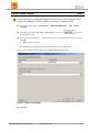
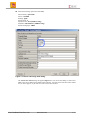
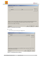
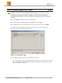
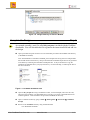
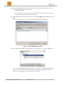
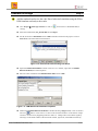
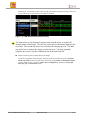
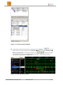
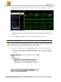
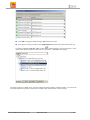
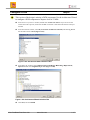
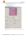
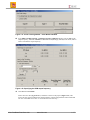
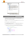
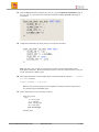
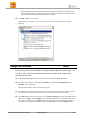
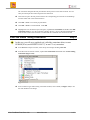
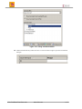
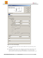
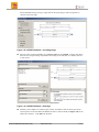
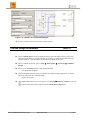
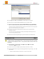
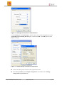
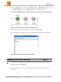
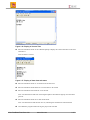
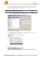
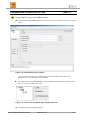
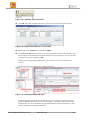
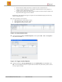
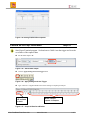
Lab 3: Xilinx PicoBlaze Flow Lab Targeting Spartan-3E Starter Kit Xilinx PicoBlaze Flow Demo Lab www.xilinx.com 1-1 Create a New Project Step 1 Create a new project targeting the Spartan-3E device that is on the Spartan-3E kit. Specify your language of choice, VHDL or Verilog, to complete the lab. Launch ISE: Select Start → All Programs → Xilinx ISE Design Suite → ISE → Project Navigator In the Project Navigator, select File → New Project… or click on Project Wizard opens . The New For Project Location, use the “…” button to browse to one of the following directories, and then click OK • VHDL users: c:\labs\lab3 The Working Directory path will also be set to the same directory automatically For Project Name, type Flow_lab, leaving Top-level source type: as HDL Figure 1-1. New Project Wizard Click Next Xilinx PicoBlaze Flow Demo Lab www.xilinx.com 1-2 Select the following options and click Next: Device Family: Spartan3E Device: xc3s500E Package: fg320 Speed Grade: –4 Synthesis Tool: XST (VHDL/Verilog) Simulator: ISE Simulator (VHDL/Verilog) Preferred Language: VHDL Figure 1-2. Device and Design Flow Dialog The Create New Source dialog will appear (Figure 1-3). You can use this dialog to create a new HDL source file by defining the module name and ports. All of the source files have been created for you in this project, so you will not create a new source file here Xilinx PicoBlaze Flow Demo Lab www.xilinx.com 1-3 Figure 1-3. Create New Source Dialog Click Next The Add Existing Sources dialog appears (Figure 1-4). Figure 1-4. Add Existing Sources Dialog Xilinx PicoBlaze Flow Demo Lab www.xilinx.com 1-4 Add an Existing Design to the Project Step 2 Add HDL source files for an example PicoBlaze design. You may review the PicoBlaze documentation to become familiar with the 8-bit microcontroller architecture and assembler. Refer to KCPSM3_manual.pdf in the KCPSM3\docs\ directory. Click Add Source and browse to the c:\KCPSM3\VHDL Select the VHDL files kcpsm3_int_test and kcpsm3 files and click Open Click Next leaving a check mark in each box for the copy to project option. Click Finish The dialogue below should appear which allows you to select a flow (none, implementation, simulation, or both) associated with each source file Figure 1-5. Choose Source Type Click OK accepting the default setting of All for both source files Note: You should see a module called int_test listed in the hierarchy view with an orange question mark. This module is a BlockRAM that will contain the instructions for the PicoBlaze controller, which will be added in a later step Xilinx PicoBlaze Flow Demo Lab www.xilinx.com 1-5 Figure 1-6. Design Hierarchy in Sources Window Complete the Design Step 3 An example assembly (.psm) file called init_test.psm is included with the PicoBlaze distribution. You will assemble this file to generate the instruction ROM and add it to the design. Open up Windows Explorer and browse to the Assembler provided in the KCPSM3 sub-directory (c:\KCPSM3\Assembler) Note: The KCPSM3.exe assembler and ROM_form* template files along with two example PSM files should reside in this directory. Keep in mind that the assembled output files will be generated in the directory containing the assembler and template files. It may be beneficial to copy the assembler and template files to your project directory. For the workshop, we will keep the files in the current location Figure 1-7. PicoBlaze Assembler Files Open the int_test.psm file using a standard text editor, such as Wordpad, and review the code, referring to the PicoBlaze 8-bit Embedded Microcontroller User Guide or KCPSM3 manual for technical guidance. These documents are provided in the docs sub-directory Open a command window by going to Start à All Programs à Accessories à Command Prompt Browse to the Assembler directory using the cd command > cd c:\KCPSM3\Assembler Xilinx PicoBlaze Flow Demo Lab www.xilinx.com 1-6 Generate the ROM definition files by assembling the example assembly application. Enter the following command at the command prompt > kcpsm3 int_test.psm Note: You should now see several files in the Assembler sub-directory starting with init_test*, including VHDL (int_test.vhd) ROM definition files Add VHDL ROM definition file to the project. Go to Project à Add Copy of Source or click on from the side button window and select either int_test.vhd file (Figure 1-8) Figure 1-8. VHDL ROM Definition Files Click Open and then OK to add INT_TEST as a VHDL Design File to the project (Figure 1-9) Figure 1-9. Hierarchical view of PicoBlaze design Note: The top-level kcpsm3_int_test file contains an instantiation of the int_test ROM definition file. After adding this source code for the int_test to the design, the red question mark in the module view will disappear as it is no longer seen as a black box Xilinx PicoBlaze Flow Demo Lab www.xilinx.com 1-7 Simulate the Design Step 4 Add the testbench and review the code. Run a behavioral simulation using the Xilinx ISIM simulator and analyze the results. Go to Project à Add Copy of Source or click on verilog) and browse to c:\KCPSM3\vhdl (or Select the testbench file (test_bench.vhd) and click Open Set the association to Simulation and click OK to add the test bench to the project. Click on Sources for: and select Behavioral Simulation Figure 1-10. Hierarchical View Including Test Bench Expand the Xilinx ISE Simulator toolbox in the Processes window, right-click on Simulate Behavioral Model, and select Properties Enter the value of 25000 for the Simulation Run Time and click OK Figure 1-11. ISIM Behavioral Simulation Properties Double-click Simulate Behavioral Model to simulate the design (Figure 1-12). Click on Zoom to Full View button. Click close to 1 us time in the waveform window. Click Zoom In couple of times to see the activity happening between 0 and 2 us. Change radix of waveforms signal by selecting it in the Name column of the waveform window, right-click, select Radix followed by Xilinx PicoBlaze Flow Demo Lab www.xilinx.com 1-8 Hexadecimal. You should see three input interrupt pulses and the displayed interrupt count value. You should also see an alternating inverted pattern displayed Figure 1-12. iSIM Behavioral Simulation Results The steps below are for illustrative purposes only, and show how to analyze the internal signals of the design. The first step shows how to add internal signals to the waveform. The second step shows how to analyze the interrupt process. The third step shows how to analyze the output waveform process. You may optionally complete these steps if you have additional time at the end of the lab. Monitor internal signals by adding them to the design You need to expand the design hierarchy and select the desired module entry [uut] in Instance and Process Name window, and then select the desired signal [address] in Simulation Objects window. Right-click on it and select Add to Wave Configuration. Similarly add interrupt, interrupt_ack, and instruction signals Xilinx PicoBlaze Flow Demo Lab www.xilinx.com 1-9 Figure 1-13. Accessing Internal Signals Change radix of address and instructions to hexadecimal. Enter 25.00us in in the tool buttons bar where 1.00us is displayed; click Simulation à Restart, followed by Simulation à Run for Specified Time to re-simulate the design. Using buttons from toolbar, you can zoom into any area of the simulator waveform window. Analyze the waveform for Interrupt Service Routine process (Figure 1-14) Interrupt acknowledgement Figure 1-14. Interrupt Service routine Xilinx PicoBlaze Flow Demo Lab www.xilinx.com 1-10 Add write_stribe signal and re-simulate the design. Analyze the output waveform process (Figure 1-15) Figure 1-15. Output Waveform Note: The int_test.log file in the Assembly directory shows the address and code for each instruction Close the simulator windows. Click No to quit the simulator without saving the run Implement the Design Step 5 Implement the design. During implementation, some reports will be created. You will look more closely at some of these reports in a later module. In the Sources in Project window, select Implementation in the Sources pane and select the toplevel design file kcpsm3_int_test.vhd (Figure 1-16). Make sure that symbol appears in front of uut instance. If not, right-click on the uut instance and select Set as Top Module. Click OK on the message Figure 1-16. Sources Window Pane Xilinx PicoBlaze Flow Demo Lab www.xilinx.com 1-11 In the Processes for Source window, double-click Implement Design (Figure 1-17) Notice that the tools run all of the processes required to implement the design. In this case, the tools run Synthesis before going into Implementation Figure 1-17. Processes for Source Window While the implementation is running, click the + next to Implement Design to expand the implementation step and view the progress. We refer to this as expanding a process After each stage is completed, a symbol will appear next to each stage: Check mark for successful Exclamation point for warnings X for errors For this particular design, there may be an exclamation point (warnings) for some steps. The warnings here are okay to ignore. Read some of the messages in the message window located across the bottom of the Project Navigator window When implementation is complete, double-click on in Processes window to review the design utilization in the Design Summary window (Figure 1-18) Xilinx PicoBlaze Flow Demo Lab www.xilinx.com 1-12 Figure 1-18. Design Summary The design implements a real-time clock maintaining time in hours, minutes and seconds together with the ability to set an alarm. The unusual feature of the design is that a UART serial communication is used to set and observe the time/alarm sending simple text commands and messages via a utility such as hyperterminal. The design understands some simple ASCII commands and even supports some editing during their entry using the backspace key on your keyboard. A command is only completed when a carriage return is entered. The design is ready to accept a command when the “KCPSM3>” prompt is displayed. The “uclock” program provided with the distribution is able to interpret upper and lower case characters by converting commands (see documentation for details) to upper case before analyzing them. Incorrect commands will result in a “syntax error” message and incorrect time values will be indicated by an “Invalid Time” message. Although it is unlikely to occur when using hyperterminal, an “overflow error” message will be generated if commands are transmitted faster than the design can process them (ie. UART receiver buffer becomes full). Click Add Source and browse to the c:\KCPSM3\VHDL Select the VHDL files uart_clock, uart_tx, uart_rx, kcuart_tx, kcuart_rx, bbfifo_16x8 and kcpsm3 files and click Open Click Next leaving a check mark in each box for the copy to project option. Click Finish The dialogue below should appear which allows you to select a flow (none, implementation, simulation, or both) associated with each source file Xilinx PicoBlaze Flow Demo Lab www.xilinx.com 1-13 Click OK accepting the default setting of All for both source files In the Sources in Project window, select Implementation in the Sources pane and select the toplevel design file uart_clockt.vhd. Make sure that symbol appears in front of uut instance. If not, right-click on the uut instance and select Set as Top Module. Click OK on the message The design requires a 55 MHz clock. Since the Spartan-3E board includes a 50 MHz oscillator, you will use the Architecture Wizard to generate a DCM with a 55 MHz output and instantiate it into the design. Xilinx PicoBlaze Flow Demo Lab www.xilinx.com 1-14 Configure a DCM Step 6 This version of the design is missing a DCM component. Use the Architecture Wizard to configure a DCM component to output a clock at 55 MHz. In the Processes for Source window, double-click Create New Source. If you do not see the Create New Source process, ensure that an HDL source file is selected in the Sources in Project window In the New Source window, select IP (CoreGen & Architecture Wizard) and enter my_dcm as the file name and click Next (Figure 1-19a) Figure 1-19a. New Source Wizard Selection Box In the Select IP window, expand FPGA Features and Design gClocking g Spartan-3E, Spartan-3A and select Single DCM_SP v9.1i (Figure 1-19b) Figure 1-19b. Architecture Wizard Selection Box Click Next, and click Finish Xilinx PicoBlaze Flow Demo Lab www.xilinx.com 1-15 In the Xilinx Clocking Wizard – General Setup window, set the following options (as shown in Figure 1-20), and click Next to continue o o o CLK0, CLKFX and LOCKED boxes: Checked RST box: Unchecked Input Clock Frequency: 50 MHz Figure 1-20. Xilinx Clocking Wizard – General Setup Window In the Xilinx Clocking Wizard – Clock Buffers window (Figure 1-21), keep the defaults and click Next Xilinx PicoBlaze Flow Demo Lab www.xilinx.com 1-16 Figure 1-21. Xilinx Clocking Wizard – Clock Buffers Window In the Xilinx Clocking Wizard – Clocking Frequency Synthesizer dialog, enter 55 MHz as the output frequency, and click Calculate to determine the M (multiply) and D (divide values) that are used to calculate the output frequency Figure 1-22. Specifying the DCM output frequency Click Next and then Finish Notice that a new file (my_dcm.xaw ) is added as a Source in the project (Figure 1-23). This source file will not be included in the design hierarchy until the component has been instantiated into one of the HDL source files. You will do this in the next step Xilinx PicoBlaze Flow Demo Lab www.xilinx.com 1-17 Figure 1-23. DCM listed in design hierarchy Instantiate the DCM into a VHDL Design Step 7 Now that you have created the necessary files, you can instantiate the DCM component into your design. Copy-and-paste the text from the Instantiation Template into uart_clock.vhd and connect the signals. In the Sources in Project window, double-click uart_clock.vhd to open the source code in the text editor Select my_dcm.xaw in the Sources in Project window In the Processes for Source window, double-click View HDL Instantiation Template to open the instantiation template in the text editor From the Instantiation Template my_dcm.vhi, copy the component declaration (begins at COMPONENT my_dcm and end after END COMPONENT;) and paste into uart_clock.vhd Xilinx PicoBlaze Flow Demo Lab www.xilinx.com 1-18 From the HDL Instantiation Template my_dcm.vhi, copy the component instantiation (begin at Inst_my_dcm: my_dcm until the end of the file) and paste into uart_clock.vhd under begin of Architecture Complete the instantiation by filling in the port connections as follows: Note: The clkin_ibufg_out port is an output that is present to support designs that use the RocketIO™ transceivers. Because the Spartan-3E device does not contain transceivers, this port will be connected to a dummy signal Add a signal declaration for the 55 MHz output of the DCM under the comment -for DCM, as follows: Signals signal clk55MHz : std_logic; note: the uart_clock.vhd design need to be updated so all design instances and processes are clocked using the clk55MHz signal Add an output pin for lock in the entity as follows: entity uart_clock is Port ( tx : out std_logic; rx : in std_logic; alarm : out std_logic; clk : in std_logic; lock : out std_logic ); end uart_clock; Xilinx PicoBlaze Flow Demo Lab www.xilinx.com 1-19 note: this lock output pin will drive the led0 on the Spartan-3E board, and is driven by the lock signal on the DCM. This will indicate to the user that the DCM has successfully locked onto the 50 MHz clock signal from the on-board oscillator Click File → Save to save the file Notice that the source file my_dcm.xaw is now inserted into the correct place in the design hierarchy Assign Pin Locations Step 8 In this step, you will use PinAhead to assign locations to the pins in the design. You will then verify in the Pad report that the pins have actually been assigned after running place & route. In the Sources in Project window, select the top-level design file uart_clock.vhd In the Processes window, expand User Constraints and double-click Floorplan I/O – PreSynthesis to open PinAhead Click yes when asked to add a UCF file to the project Click Close to close the introductory window if it shows up (You can uncheck the box if you do not want to see this introductory window every time you invoke PinAhead from ISE) In the I/O Ports window select tx signal. In the I/O Port Properties window type m14 in the site field and click Apply. Select configure tab and select LVTTL as the I/O standard, and select 8 mA as the drive strength. Click Apply button to assign these properties. Similarly enter the pin constraints for other pins in the design as shown in the I/O Ports list window (Figure 1-24) Xilinx PicoBlaze Flow Demo Lab www.xilinx.com 1-20 Figure 1-24. Enter Pin Location Constraints Listed below are descriptions for the I/O signals that you have just assigned. The complete pinout for the Spartan-3E starter kit can be found in the user manual o o o o o clk : connected to 50 MHz oscillator lock : connected to led0 alarm : connected to led1 rx : connected to pin that receives serial data from Maxim MAX3232 tx : connected to pin that transmits serial data to Maxim MAX3232 View your pin assignments in relation to the internal logic. In the I/O Ports window select a pin (e.g. rx) and click on Fit Selection button (). Notice that the FloorPlan window shows the selected I/O and the Device Package window shows the (Figure 125) Figure 1-25. Device and Package Windows Xilinx PicoBlaze Flow Demo Lab www.xilinx.com 1-21 The colored bar alongside the I/O pins indicates which pins are in the same I/O bank. You can easily see which pins have been assigned to the same bank. Click each I/O pin in the I/O port and observe the corresponding pin in the Device and Package windows when click on Fit Selection button Click File → Save to save these pin placements Click File → Exit to close PinAhead. Click OK Highlight the UCF file in the Project Navigator, expand User Constraints and double-click Edit Constraints (Text) to view the constraints created in the uart_clock.ucf file through PlanAhead. View the text version of the UCF file to confirm that the constraints were written to the file Enter the Global Timing Constraints Step 9 In this step, you will use a graphical tool, called the constraints editor, to enter PERIOD (20 ns) and OFFSET IN/OUT (7 ns and 7.5 ns) constraints. In the Sources in Project window, select the top-level design file uart_clock.vhd. In the Processes for Source window, expand User Constraints and double-click Create Timing Constraints (Figure 1-26) Figure 1-26. Processes for Source Window In the constraint Type under Timing Constraints window, select Global (see Figure 1-27) to list the clock domains in the design Xilinx PicoBlaze Flow Demo Lab www.xilinx.com 1-22 Figure 1-27. Timing Constraints Editor Double-click Period entry under the Clock net name window on right to open the Clock Period dialogue Xilinx PicoBlaze Flow Demo Lab www.xilinx.com 1-23 Figure 1-28. Clock Period dialogue Accept the default settings of 20ns (since we have 50 MHz clock source) and 50% duty cycle by clicking OK Select Ports in Constraint Type window, and double-click the white space under the Pad to setup column in the right side window to invoke the Offset In Wizard. Leave the default settings (System synchronous, SDR, and Rising edge) and click Next after reviewing the description. Note Xilinx PicoBlaze Flow Demo Lab www.xilinx.com 1-24 that the PicoBlaze design is using a single clock for the entire design, where all registers are clocked on the rising edge Figure 1-29. OFFSET IN Wizard – Clock Edge Page Enter the value of 7 ns for OFFSET IN (see Figure 1-30) and click Finish. Note that this design does not have stringent timing requirements for clocking in external data, so a random value of 7 ns was chosen Figure 1-30. OFFSET IN Wizard – Data Page Similarly, select Outputs in Constraint Type window, and double -click the white space under Clock to pad to invoke the Offset Out Wizard and enter a value of 7.5 ns (see Figure 3-8) for the Offset Out constraint. Click OK when finished Xilinx PicoBlaze Flow Demo Lab www.xilinx.com 1-25 Figure 1-31. OFFSET OUT constraints dialogue Save the constraints and close the timing constraints editor Test the Design in Hardware Step 10 Open the uclock.psm file using a standard text editor, such as Wordpad, and review the code, refering to the PicoBlaze 8-bit Embedded Microcontroller User Guide or KCPSM3 manual for technical guidance. These documents are provided in the docs sub-directory Open a command window by going to Start à All Programs à Accessories à Command Prompt Browse to the Assembler directory using the cd command > cd c:\KCPSM3\Assembler Generate the ROM definition files by assembling the example assembly application. Enter the following command at the command prompt > kcpsm3 uclock.psm Add VHDL ROM definition file to the project. Go to Project à Add Copy of Source or click on from the side button window and select either uclock.vhd file (Figure 1-8) Xilinx PicoBlaze Flow Demo Lab www.xilinx.com 1-26 Click Open and then OK to add uclock.vhd as a VHDL Design File to the project Select the top-level design file uart_clock.vhd in the Sources in Project window In the Processes for Source window, expand the Implement Design process, expand Place & Route, expand Back-Annotate Pin Locations and double-click View Locked Pin Constraints The Project Navigator automatically determines which processes must be run, and it will open the report once the Place & Route process is completed Scroll down in the report and confirm that the pin numbers for the I/O signals match the assignments you made You can also view the pin assignments by clicking on Pinout Report under Design Overview section of the Design Summary window Double-click on Generate Programming File to generate bitstream file. (Error IBUF CLK). Configure de FPGA Step 11 Configure and start a hyperterminal session. Connect and power the board. Generate the bitstream and configure the FPGA. Verify operation of the real-time UART clock in hardware. Open a hyperterminal session by going to Start à All Programs à Accessories à Communications à HyperTerminal Give the session a name, click OK, and specify COM port connection (ie. COM1) Click the Configure button and specify the following parameters for the port settings. Click OK when finished • Baud rate of 38400, 8 data bits, No parity bits, 1 stop bit, No flow control Xilinx PicoBlaze Flow Demo Lab www.xilinx.com 1-27 Figure 1-32. Settings for Serial Port Communications Click the Settings tab, the ASCII Setup tab and then click so that a check mark appears next to the Append line feeds to incoming line ends option, and then click OK. Click OK again to exit the properties dialogue Figure 1-33. ASCII Settings for Serial Port Connection Connect the cables (power, USB, and rs232) and power the board Select uart_clock.vhd, expand Configure Target Device, and double-click on Manage Configuration Project (iMPACT) Xilinx PicoBlaze Flow Demo Lab www.xilinx.com 1-28 When the iMPACT opens, double-click on Boundary Scan () in iMPACT Flow window. Click on Initialize Chain () button. Click YES and then browse to the project directory Select uart_clock.bit file for the xc3s500e (first device in JTAG chain). Next, click NO as we do not want to attach the PROM files, and click bypass for the remaining devices, and then click OK Figure 1-34. JTAG Chain with assigned configuration files Right-click on the xc3s500e in the iMPACT window and select Program Note: You should now see the KCPSM3> prompt in the hyperterminal window. If not, then hit Enter key Figure 1-35. Serial Communication with PicoBlaze Operate the UART Real-Time Clock Step 12 You will issue commands to operate the UART real-time clock, as specified in the UART_real_time_clock.pdf file. Enter the command “time” at the command prompt to display the current time in the form of hh:mm:ss Xilinx PicoBlaze Flow Demo Lab www.xilinx.com 1-29 Figure 1-36. Display of Current Time Enter the command “alarm” at the command prompt to display the current alarm time in the form of hh:mm:ss Note: the alarm is inactive Figure 1-37. Display of alarm time and status Enter the command “alarm on” for the alarm to become active Enter the command “alarm 00:00:30” to set the alarm to 30 seconds Enter the command “time 00:00:00” to set the time Note: You should notice that led1 on the Digilent Spartan-3E board will light up once the alarm goes off. Enter the command “alarm off” to shut off the alarm. Note: You should notice that the led1 turns on, indicating that the alarm has been disarmed. Close iMPACT program without saving the project and close ISE Xilinx PicoBlaze Flow Demo Lab www.xilinx.com 1-30 You will extend the lab design by adding a ChipScope ILA core to the PicoBlaze output bus. Next, you will setup the trigger to capture data when text is entered via hyperterminal. You should see the resulting text displayed in ChipScope when the buffer is full. Create a New ChipScope-Pro Source Step 13 Create a new ChipScope Definition and Connection source by selecting Project à New Source and entering the name uart_clock_cs. Click Next to continue. Figure 1-38. New Source Dialog Box Select uart_clock as the source. Click Next and then Finish. A ChipScope-Pro source will be added to the Sources in Project window. Figure 1-39. ChipScope Definition and Connection (.cdc) added to VHDL Project Xilinx PicoBlaze Flow Demo Lab www.xilinx.com 1-31 Configure and Connect an ILA Core Step 14 Connect the ILA core to the PicoBlaze output. Double-click the uart_clock_cs.cdc file in the sources in project window to open the core inserter project. Figure 1-40. ChipScope-Pro Core Inserter Note: Projects saved in the Core Inserter hold all relevant information about source files, destination files, core parameters and core settings. Click Next and then click New ILA Unit. Notice in the left hand window how an instance of the ILA core, U0:ILA, is added to the system. Figure 1-41. Insert a new integrated logic analyzer (ILA) Unit Click Next to setup the trigger parameters Xilinx PicoBlaze Flow Demo Lab www.xilinx.com 1-32 Each ILA or ILA/ATC core can have up to 16 separate trigger ports that can be setup independently. The individual trigger ports are buses that are made up of individual signals or bits that can range from 1 to 256 bits. Each trigger port can be connected to 1 to 16 match units. A match unit is a comparator that is connected to a trigger port and is used to detect events on that trigger port. The results of one or more match units are combined together to form the overall trigger condition event that is used to control the capturing of data. The different comparisons or match functions that can be performed by the trigger port match units depend on the type of match unit. The ILA and ILA/ITC cores support six types of match units. In this lab, you will setup the ILA core to trigger via some UART control signals. Set the following ILA trigger parameters as follows and then click Next Trigger Input and Match Unit Settings • Number of input trigger ports: 3 Trigger Port TRIG0 TRIG1 TRIG2 Trigger Width 1 1 1 # Match Units 1 1 1 Counter Width Disabled Disabled Disabled Match Type Basic Basic Basic Trigger Condition Settings Enable Trigger Sequencer: Checked (This allows you to specify a sequence of events to enable triggering) Max Number of Sequencer Levels: 2 Storage Qualification Condition Settings Enable Storage Qualification: Checked (This allows you to specify which data will be stored in the internal buffer) Xilinx PicoBlaze Flow Demo Lab www.xilinx.com 1-33 Figure 1-42. Specify the Trigger Parameters The maximum number of data sample words that the ILA core can store in the sample buffer is called the data depth. The data depth determines the number of data width bits contributed by each block RAM unit used by the ILA unit. The maximum number of data sample words that can be captured depends on the number and size of block RAM, which varies according to device family and density. Set the following capture parameters and click Next • • • • Data Depth: 512 Sample On: Rising clock edge Data Same as Trigger Port: unchecked Data Width: 8 Xilinx PicoBlaze Flow Demo Lab www.xilinx.com 1-34 Figure 1-43. Specify Trigger Parameters The net connections tab allows you to choose the signals to connect to the ILA core. If trigger is separate from data, then clock, trigger, and data must be specified. Connections that have not been made will appear in red. Figure 1-44. Unconnected Net Connections Click the Modify Connections tab Xilinx PicoBlaze Flow Demo Lab www.xilinx.com 1-35 ChipScope ILA ports available for connection List of design nets Figure 1-45. Net Connections The Select Net dialog provides an easy interface to choose nets to connect to the ILA, ILA/ATC or ATC2 cores. The hierarchical structure of the design can be traversed using the Structure/Nets pane. All the design’s nets of the selected structure hierarchy appear in the table at the lower left pane. The Clock Signals and Trigger/Data Signals tabs illustrate the net connections between the design and the ILA core. With the Clock Signals tab under Net Selections selected, highlight the entry for clk55MHz in the listing of nets and click the Make Connections button to connect the clock signal in the design to the clock port of the ILA core Figure 1-46. Connect the clock Xilinx PicoBlaze Flow Demo Lab www.xilinx.com 1-36 Click the Trigger Signals tab, and connect the three trigger ports as follows: TP0: rx_data_present (this signal indicates that data is present in the uart_rx module TP1: read_from_uart (input to uart_rx that indicates that a read operation will occur) TP2: write_to_uart (input to uart_tx that indicates that a write operation will occur) Click the Data Signals tab and connect the output port of the PicoBlaze controller to the data port of the ILA core (see Figure 1-50), and click OK Figure 1-47. Connect the PicoBlaze output port You will notice that the Clock, Trigger, and Data ports under Net Connections are highlighted in black, indicating valid connections. Click Return to Project Navigator and save the file Figure 1-48. Connection between Design and ILA core Established Specify ChipScope Analyzer Options Step 15 You will download the bitstream using ChipScope and configure the ILA core to trigger when the UART reads text from hyperterminal. With the top-level file (uart_clock.vhd) selected, double-click on Analyze Design Using ChipScope in the Processes window Click the Open Cable/Search JTAG Chain button Xilinx PicoBlaze Flow Demo Lab www.xilinx.com 1-37 Figure 1-49. Establish JTAG Connection Click OK, noting that the Spartan-3E device is the first device in the chain of three devices Figure 1-50. Impact Detects Devices in JTAG Chain Right Click on the xc3s500e device and select configure Click Select New File and select the uart_clock.bit bitstream file from the project directory. Note that the import cdc file field shows the cdc file located in the project directory. The user will need to create a bus (out_port). Right click OK Double-click on Trigger Setup and Waveform entries in Project Tree to open the respective windows The ChipScope Pro Analyzer interface consists of four parts: Figure 1-51. ChipScope Analyzer Window Each ChipScope Pro ILA, ILA/ATC, and IBA core has its own Trigger setup window, which provides a graphical interface for the user to setup triggers. The trigger mechanism inside each ChipScope Pro core can be modified at run-time without having to recompile the design. There are three components to the trigger mechanism: Xilinx PicoBlaze Flow Demo Lab www.xilinx.com 1-38 • • • Match Functions: Defines the match or comparison value of each match unit Trigger Conditions: Defines the overall trigger condition based on a binary equation or sequence of one or more match functions Capture Settings: Defines how many samples to capture, how many capture windows, and the position of the trigger in those windows In this design, you will setup the triggers to capture text at the PicoBlaze output port, after being entered via hyperterminal. Specify the Match Units as follows: • M0:TriggerPort0 (rx_data_present): Value 1 • M1:TriggerPort1(read_from_uart): Value 1 • M2:TriggerPort1(write_to_uart): Value 1 Figure 1-52. Setup the Match Units Click the field under Trigger Condition Equation, set the equation M0 → M1 in the Sequencer tab, and then click OK Figure 1-53. Trigger Condition Equation Check the field next to Storage Qualification, select the AND Equation, and check M2. Click OK. This will enable the ILA core to capture data in the buffer only when data is present, and not on every single clock edge Xilinx PicoBlaze Flow Demo Lab www.xilinx.com 1-39 Figure 1-54. Storage Qualification Equation Perform an On-Chip Verification Step 16 Start Hyper-Terminal program. Set baud rate to 38400. Arm the trigger and view the waveforms of the captured data. Set the buffer depth to 16 Figure 1-55. Select Buffer Depth Cick the Apply Settings and Arm Trigger button Figure 1-56. Apply Settings and Arm Trigger Type “alarm on“ in hyperterminal and view the message in ChipScope Analyzer Right click and set Radix to ASCII Buffer setup to capture 16 samples Figure 1-57. Output in Waveform Window Xilinx PicoBlaze Flow Demo Lab www.xilinx.com 1-40