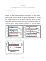
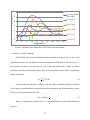
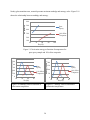
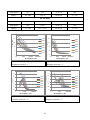
1
THERMALLY STIMULATED DEPOLARIZATION CURRENT EVALUATION OF MOLDING COMPOUNDS Shunli Zhao Thesis Prepared for the Degree of MASTER OF SCIENCE UNIVERSITY OF NORTH TEXAS May 2014 APPROVED: Nandika A. D’Souza, Major Advisor Tae Youl Choi, Committee Member Xun Yu, Committee Member Yong Tao, Chair of the Department of Mechanical and Energy Engineering Costas Tsatsoulis, Dean of the College of Engineering Mark Wardell, Dean of the Toulouse Graduate School Zhao, Shunli. Thermally Stimulated Depolarization Current Evaluation of Molding Compounds. Master of Science (Mechanical and Energy Engineering), May 2014, 74 pp., 7 tables, 76 figures, reference, 38 titles. TSDC (thermally stimulated depolarization current) is one of the most important and popular technique for investigating electret materials. TSDC technique can indicate the magnitude of polarization and depolarization, relaxation time, charge-storage, glass transition, and activation energy. To fully investigate polarization and relaxation for pure epoxy and filled epoxy materials, a TSDC system was built and verified by the research. The article describes the building processes and verification of the TSDC system. TSDC, TSPC, and TWC tests data for epoxy and filled epoxy samples are presented in the article. To compare TSDC technique with other related techniques, DEA (dielectric analysis), DMA (dynamic mechanical analysis), and DSC (differential scanning calorimetry) tests are introduced. Copyright 2014 by Shunli Zhao ii ACKNOWLEDGEMENTS This thesis has been made possible by three important groups of people in my life. Professors Firstly, I would like to express the greatest gratitude to my adviser, Dr. Nandika Anne D’Souza, who supported my whole graduate study. She taught me a lot of wisdoms, which are not only for study but also for life. Those wisdoms will guide my whole life. It is my honor to be her students. I would like to acknowledge my thesis committee members Dr. Xun Yu and Dr. Tae Youl Choi. Dr. Choi provided me with excellent support to enable me to select parts for TSDC system. Thanks for Dr. Choi’s great contribution on building TSDC system. Dr. Xun Yu enabled me to learn controls for the system design. Family and Friends Thank my parents, who gave me life and raised me up. All the glory I got is belonged to them. Thank my sister for taking care of our parents during the time I am away. Thanks my lab mate Mangesh Nar, who gave me help and guide me all the time. Thanks Andres Garcia, who work together with me and made the system more perfect. Thanks Bing Yang for his support. Sponsor Thanks SRC (Semiconductor Research Corporation) sponsored our search (SRC Grant Task 2071.026: Thermally Stimulated Current Evaluation of Molding Compounds Used in High Voltage Applications). Thanks Denison, Marie and Nguyen. Luu from Texas Instrument Company. Thanks for their patient guide and support. iii TABLE OF CONTENTS Page ACKNOWLEDGMENTS ............................................................................................................. iv LIST OF TABLES ......................................................................................................................... iv LIST OF FIGURES ....................................................................................................................... iv CHAPTER 1. INTRODUCTION ....................................................................................................1 CHAPTER 2. LITERATURE REVIEW .........................................................................................3 2.1 Molding Compounds Materials .....................................................................................3 2.2 TSDC Concept ...............................................................................................................5 2.3 PID Control ....................................................................................................................7 2.3.1 Proportional Band ...........................................................................................7 2.3.2 Integral Time ...................................................................................................8 2.3.3 Derivative Time ..............................................................................................9 2.3.4 PID Adjustments .............................................................................................0 CHAPTER 3. TSDC SYSTEM INSTRUMENTATION DESIGN ..............................................12 3.1 Overview of the Whole System ...................................................................................12 3.2 TSDC Cell....................................................................................................................13 3.3 Main Chamber .............................................................................................................14 3.4 Heating Unit .................................................................................................................16 3.4.1 Gas Heater .....................................................................................................18 3.4.2 Nitrogen Gas .................................................................................................19 3.4.3 Temperature Controller.................................................................................19 3.5 Cooling Unit.................................................................................................................22 iv 3.6 Electrical Unit (Voltage Supply & Current Measurement Unit) .................................24 3.6.1 Capabilities and Features Overview .............................................................24 3.6.2 Guarding .......................................................................................................25 3.6.3 Voltage Source Basic Operation ...................................................................26 3.6.4 Configuring V-Source ...................................................................................27 3.6.5 Current Measurements .................................................................................28 3.6.6 Interlock and Test Fixtures ...........................................................................29 3.6.7 Connecting Cable ..........................................................................................30 3.6.8 LEMO Connector .........................................................................................31 3.7 Data Acquisition System..............................................................................................32 3.7.1 Analog Signal and Digital Signal .................................................................32 3.7.2 Temperature Data Logger .............................................................................33 3.7.3 IEEE 488 (GPIB card) Communication .......................................................35 3.7.4 Labview.........................................................................................................36 3.8 Overall Schematic Diagram of TSDC System ............................................................38 CHAPTER 4. TSDC EXPERIMENTAL PROCEDURES ...........................................................39 4.1 Sample Preparation ......................................................................................................39 4.1.1 Sample Material ............................................................................................39 4.1.2 Sample Curing ..............................................................................................41 4.1.3 Sputtering .....................................................................................................41 4.2 Procedure of TSDC Experiment .................................................................................44 4.3 TSPC Experiment .......................................................................................................45 4.4 Window Polarization ..................................................................................................46 v CHAPTER 5. TSDC EXPERIMENT DATA ON EPOXY AND FILLED EPOXY ....................49 5.1 TSDC Experiment Data ..............................................................................................49 5.2 TSPC Experiment Data ................................................................................................51 5.3 Windows Polarization .................................................................................................52 5.4 Analysis of TSDC Technique ......................................................................................53 CHAPTER 6 ALTERNATIVE TECHNIQUES TO MEASURE THERMAL TRANSITIONS IN EPOXY AND FILLED EPOXY .....................................................................60 6.1 Dielectric Analysis .......................................................................................................60 6.2 DMA – 3 Point Bending Test .....................................................................................64 6.3 DSC Test ......................................................................................................................67 6.4 Moisture Test ...............................................................................................................68 CHAPTER 7 SUMMARY.............................................................................................................70 REFERENCES ..............................................................................................................................71 vi LIST OF TABLES Page Table 3.1: Port Function List of Main Chamber ............................................................................15 Table 4.1 Specification of 1556 US Epoxy Resin .........................................................................40 Table 4.2 Specification of Msds Aradur 2964 US Agent ..............................................................40 Table 4.3 TSDC Experiment Parameter for Epoxy and Composite Samples................................45 Table 5.1 Curve-Coordinate Area Comparison between TSDC and TSPC .................................51 Table 6.1. DEA Test – Temperature Scan Data Analysis..............................................................61 Table 6.2. DMA Test – Temperature Scan Data Analysis ............................................................65 vii LIST OF FIGURES Page Figure 2.1: The principal set-up of a typical TSDC experiment......................................................6 Figure 2.2: Proportional band feature of CN63100 controller .........................................................8 Figure 2.3: Integral time ..................................................................................................................9 Figure 2.4: Derivative time ............................................................................................................10 Figure 2.5: Typical response curve ................................................................................................11 Figure 2.6: Process response extremes ..........................................................................................11 Figure 3.1: Overview of whole TSDC system ...............................................................................12 Figure 3.2: TSDC cell ....................................................................................................................14 Figure 3.3: 3D design of main chamber and real picture ...............................................................16 Figure 3.4: Dimension of main chamber .......................................................................................16 Figure 3.5: Overview of heating unit .............................................................................................18 Figure 3.6: OMEGA – AHP series gas heater ...............................................................................18 Figure 3.7: OMEGA-CN63100 temperature controller ................................................................20 Figure 3.8: OMEGA-CN63100 temperature controller – SPRP mode diagram ...........................22 Figure 3.9: TSDC system - SPRP heating mode temperature curve .............................................22 Figure 3.10: Overview of heating unit of TSDC system ..............................................................23 Figure 3.11: Overview of electrical unit of TSDC system ............................................................24 Figure 3.12: Connection diagram between TSDC cell and 6517B meter......................................25 Figure 3.13: Guarding diagram of Keithley 6517B meter .............................................................26 Figure 3.14: Current measurement diagram of Keithley 6517B meter .........................................29 Figure 3.15: Interlock diagram of Keithley 6517B meter..............................................................30 viii Figure 3.16: Cable used in TSDC system ......................................................................................30 Figure 3.17: LEMO connectors used in TSDC system..................................................................31 Figure 3.18: Temperature signal acquisition unit - PT-104A data logger .....................................34 Figure 3.19: GPIB card for Keithley 6517B meter .......................................................................35 Figure 3.20: LabVIEW software interface.....................................................................................37 Figure 3.21: LabVIEW software program for TSDC system ........................................................37 Figure 3.22: Diagram of whole TSDC system...............................................................................38 Figure 4.1 Tempered glass mold for epoxy sample .......................................................................41 Figure 4.2 Model 5100 sputtering coater .......................................................................................43 Figure 4.3 Epoxy film sample for TSDC experiment. left: before sputtering; right: after Sputtering .....................................................................................................................43 Figure 4.4 Schematic procedure of epoxy TSDC experiment ......................................................44 Figure 4.5 Schematic procedure of epoxy TSPC experiment ........................................................46 Figure 4.6 Schematic procedure of epoxy window polarization experiment ................................48 Figure 5.1 TSDC curve-600V polarization....................................................................................49 Figure 5.2 TSDC curve-400V polarization....................................................................................49 Figure 5.3 TSDC curve-200V polarization....................................................................................49 Figure 5.4. Pure epoxy sample depolarization current comparison among different polarization Voltages ......................................................................................................................50 Figure 5.5. Epoxy-silica composite sample depolarization current comparison among different polarization voltages ...................................................................................................50 Figure 5.6 TSPC 200V...................................................................................................................51 Figure 5.7 TSDC 200V ..................................................................................................................51 ix Figure 5.8 Window polarization data of pure epoxy sample .........................................................50 Figure 5.9 Window polarization data of 10% silica composite sample .........................................51 Figure 5.10 BFG area method to calculate residual polarization...................................................55 Figure 5.11 τi vs 1/T plot for pure epoxy sample...........................................................................56 Figure 5.12 τi vs 1/T plot for 10% silica composite sample ..........................................................56 Figure 5.13 log(τi) vs 1/T plot for pure epoxy sample ...................................................................57 Figure 5.14 log(τi) vs 1/T plot for 10% silica composite sample ..................................................57 Figure 5.15 Activation energy as function of temperature for pure epoxy sample and 10% silica composite...........................................................................................................58 Figure 5.16 Enthalpy value as function of polarization temperature .............................................58 Figure 5.17 Entropy value as function of polarization temperature ..............................................58 Figure 5.18 Enthalpy and entropy relationship ..............................................................................59 Figure 6.1 DEA temperature scan test – e’ ....................................................................................61 Figure 6.2 DEA temperature scan test – e’’ ..................................................................................61 Figure 6.3 DEA temperature scan test – detan delta .....................................................................61 Figure 6.4 Pure epoxy sample DEA frequency scan test – e’ .......................................................62 Figure 6.5 10% silica filler sample DEA frequency scan test – e’ ...............................................62 Figure 6.6 Pure epoxy sample DEA frequency scan test – e’’ .....................................................62 Figure 6.7 10% silica filler sample DEA frequency scan test – e’’ ..............................................62 Figure 6.8 Pure epoxy sample DEA frequency scan test – detan delta .........................................63 Figure 6.9 10% silica filler sample DEA frequency scan test – detan delta ..................................63 Figure 6.10 Master curve of DEA test ...........................................................................................63 Figure 6.11 Shift factor of DEA master curve ...............................................................................63 x Figure 6.12 DMA – 3-point bending test – E’ ..............................................................................65 Figure 6.13 DMA – 3-point bending test – E’’ .............................................................................65 Figure 6.14 DMA – 3-point bending test – tan delta .....................................................................65 Figure 6.15 Master curve of DMA test ..........................................................................................66 Figure 6.16 Shift factor of DMA master curve .............................................................................66 Figure 6.17 DSC curve ..................................................................................................................68 Figure 6.18 Sample moisture gain weight curve ...........................................................................68 Figure 6.19 Pure epoxy humidity test - e' ......................................................................................69 Figure 6.20 10% silica sample humidity test - e' ...........................................................................69 Figure 6.21 Pure epoxy humidity test - e'' .....................................................................................69 Figure 6.22 10% silica sample humidity test - e'' .........................................................................69 Figure 6.23 Pure epoxy humidity test - detan delta .......................................................................69 Figure 6.24 10% silica sample humidity test - detan delta ............................................................69 xi CHAPTER 1 INTRODUCTION Thermally stimulated depolarization current measurement is one of the most important methods for identifying and characterizing relaxation processes, charge-storage, and chargedecay processes in electrified dielectrics and electrets [1]. The charge of electrets may be generated by various mechanisms: orientation of permanent dipoles (in polar materials), trapping of charges by structural defects and impurity centers, and build-up of charges near heterogeneities such as the amorphous-crystalline interfaces in semi-crystalline polymers, and the grain boundaries in polycrystalline materials [2]. To study the charge decay and contribution of electrets under constant heating rate, TSDC technique was introduced. The decay processes are thus investigated as a function of temperature instead of time [3]. At room temperature, charge decay measurements are rather time consuming, because at such low temperatures the dipoles and charges remain virtually immobile. However, when the environment around the electret becomes mobile, the dipoles and charges quickly regain their freedom of motion [4]. Thermal stimulation of the discharge therefore shortens the measurement considerably. During such heat-stimulated discharge, a metal connection between two electrodes generates a weak current that shows a number of peaks when recorded as a function of temperature. The shape and location of these peaks are characteristic of the electrets’ charges storage mechanisms. Analysis of the peaks yields detailed information on the permanent dipoles (density, relaxation time, activation energy) and trapping parameters (energies, concentration, and capture cross section of traps). To further isolate individual relaxations related to the macroscopic relaxation, Lacabanne and Chatain proposed a modified TSDC method termed thermal sampling or window 1 polarization [2]. They attempted to experimentally deconvolute individual relaxation contributions from the global relaxation spectra. The relaxation time-temperature relationship associated with each window is used to isolate elementary Debye type relaxations of the molecules over the entire relaxation spectrum [3]. Physically, the existence of multiple relaxations can be explained by several mechanisms, including dipole-dipole interactions, variations in size and shape of the rotating dipolar entities, anisotropy of the internal field in which the dipoles reorient (internal rotation, bending and twisting in polymers etc.) [4]. This technique is a further development of the attempt by Bucci to isolate overlapping relaxations [4]. To isolate the transitions for a material having two peak temperatures Tm1 and Tm2 they polarized the material at Tp1 such that Tm1< Tp1 < Tm2 to allow the dipoles associated with Tm1 to be polarized but those associated with Tm2 to be undisturbed. The TSDC curve would then show only the relaxation associated with Tm1. The relaxation associated with Tm2, could be isolated by polarizing the material at Tp2 such that Tm2 < Tp2 and removing the field at Td such that Tm1 < Td < Tm2. Window polarization has recently been utilized to probe space charge relaxations. Space charge relaxations were demarcated from glass transition relaxation by a minimal shift in peak temperatures for different temperature windows. Although TSDC has a relatively short history, it has already evolved into a basic tool for the identification and evaluation of dipole reorientation processes and of trapping and recombination levels [5]. Its rapid growth has been spurred on by the fact that charge-trapping and charge-transport phenomena are not only of vital importance for electrets, but also for materials used in thin films, photoconductors, electro-optical devices, etc. 2 CHAPTER 2 LITERATURE REVIEW The objective of this research is molding compounds materials; section 2.1 shows the background information for molding compounds materials. The basic principle and history for TSDC technique is discussed in section 2.2. PID concept and application is discussed in section 2.3. 2.1 Molding Compounds Materials Mold compounds are the plastics used to encapsulate many types of electronic packages, from capacitors and transistors to central processing units (CPUs) and memory devices. The modern mold compound has evolved into a complex formulation containing as many as 20 raw materials and multiple processing steps, each statistically controlled to yield a uniform and predictable end product [5]. At the most basic level, mold compounds contain five classes of raw materials. Organic resins are typically meltable. Fillers are non-melting inorganic materials. Catalysts accelerate the cure reaction [5]. The mold release material allows the naturally adhesive resin to come out of the mold. The final raw material is a pigment or colorant. Other materials, such as flame retardants, adhesion promoters, ion traps and stress relievers are added to the mold compound as appropriate. The most popular molding compounds are generally composite materials consisting of epoxy resins, phenolic hardeners, silica, catalysts, pigments, and mold release agents [6]. Epoxy molding compounds for microelectronic devices have been and will continue to be the main stay of encapsulation materials in view of their cost and productivity advantages. On the other hand, as chip sizes become larger due to increased integration of devices, compacter packages are in 3 demand to realize the higher integration. Advances in surface mounting technologies demand encapsulation materials which have extremely low thermal stress and excellent stability at the elevated temperatures used in reflow soldering. Critical properties considered when selecting a molding compound include its glass transition temperature, moisture absorption rate, flexural modulus/strength, coefficient of thermal expansion, thermal conductivity, and adhesion properties [7]. There are many types of molding compounds used in the semiconductor industry today. General-purpose molding compounds with relatively high flexural strengths but exert relatively larger stresses to the device may be used for large and thick packages such as the PDIP and PLCC. Low to ultra-low stress molding compounds is preferred for the encapsulation of thin packages. High-thermal conductivity molding compounds, on the other hand, are required to encapsulate high-power devices. Molding compounds used for surface mount devices may have a low moisture absorption rate or a high flexural strength at board-mounting temperatures, or a combination of both in order to prevent popcorn cracking. Proper molding compound selection will prevent problems associated with manufacturability, package stress, package cracking, and interfacial delamination. Mold compounds have evolved over the years to keep pace with industry needs [7]. Each innovation in chip or package design required a similar change in the design of the encapsulant. In 1969, encapsulants typically were filled with fused silica at about a 68 percent w/w loading. Currently, materials are filled with 90 percent fused silica. This shift was not made for reasons of cost, but driven by end-user performance requirements. Over the last decade, every raw material and process in mold compounds has been re-examined — and almost all have seen major changes. 4 2.2 TSDC Concept As summarized by D’Souza [1][2], thermally stimulated discharge (TSD) measures the dielectric relaxation of materials through measurement of a field induced thermally stimulated depolarization current (TSDC), also referred to as ionic thermo-current technique [8]. Under simultaneous application of electric field during a temperature ramp, the orientation of the dipoles results in the formation of an electret. The first electrets were formed by Eguchi. The use of TSDC is in no way limited to polymeric materials [9]. However, since dielectric relaxation is due to hindrance of the motions of the permanent dipoles and free charges by frictional forces, application to polymers has been widespread. TSDC measurements have been traced to Frei and Groetzinger in a review by Vanderschueren and Gasiot [10]. The technique was applied to a series of complex systems by numerous researchers including Gross, Wikstroem, Gubkin and Matsonashvili and Murphy [11]. Relating these relaxations to fundamental mechanisms of charge storage and release in nonmetallic systems was initiated by Bucci and Fieschi. One of the first detailed investigations on its potential in polymers was initiated by van Turnhout. As Vanderschueren points out, this technique was developed independently by several researchers. It is worthwhile to clarify that TSD is also referred to as electret thermal analysis, thermalcurrent spectra, thermally stimulated depolarization and thermally activated depolarization. Applications to amorphous and semicrystalline polymers have been reviewed by Bernes. The sensitivity of TSD to small fractions of uncured material extends its use to thermosetting systems. In addition, TSD is useful in establishing differences based on tactility and chemical structure, water absorption, interfaces in composites etc. Its applicability to a wide variety of parameters has been recently reviewed [12]. 5 The principal set-up of a TSDC experiment is shown in figure 2.1. The sample is placed between two electrodes of a sample capacitor. The sample can be polarized (charged) by applying a voltage to the sample under the temperature higher than glass transition. After cooling down system quickly to freeze the polarization, sample will be heated up again at a constant heating rate, during this heating process, the depolarization current can be measured as a function of time and/or temperature. Figure 2.1: The principal set-up of a typical TSDC experiment (from Novocontrol manual). A TSDC system should have these functions and capabilities: (a) Provide an enclosed and stable environment for testing; (b) Be able to control sample temperature as experiment’s requirement: fast heating, slow heating, and fast cooling; (c) High DC voltage source to supply polarization voltage to sample (d) Contain accurate Pico-ammeter to measure depolarization current (e) Data acquisition system. 6 2.3 PID Control 2.3.1 Proportional Band Proportional band is defined as the “band” (range) the process changes to cause the percent output power to change from 0% to 100% [13]. The band may or may not be centered about the setpoint value depending upon the steady state requirements of the process. The band is shifted by manual offset or integral action (automatic reset) to maintain zero error. Proportional band is expressed as percent of input sensor range [14]. Example: as shown in figure 2.2, thermocouple type T with a temperature range of 600°C is used and is indicated in degrees Celsius with a proportional band of 5%. This yields a band of 600°C X 5% = 30°C [22]. The proportional band should be set to obtain the best response to a disturbance while minimizing overshoot. Low proportional band settings (high gain) result in quick controller response at expense of stability and increased overshoot. Settings that are excessively low produce continuous oscillations at setpoint. High proportional band settings (low gain) result in a sluggish response with long periods of process “droop.” A proportional band of 0.0% forces the controller into ON/OFF control mode with its characteristic cycling at setpoint. 7 Figure 2.2: Proportional band feature of CN63100 controller. 2.3.2 Integral Time Integral time is defined as the time, in seconds, in which the output due to integral action alone equals the output due to proportional action with a constant process error [15]. As long as a constant error exists, integral action repeats the proportional action each integral time. Integral action shifts the center point position of the proportional band to eliminate error in the steady state. The units of integral time are seconds per repeat [22]. One of the typical integral time diagram is shown in figure 2.3. Integral action (also known as “automatic reset”) changes the output power to bring the process to setpoint. Integral times that are too fast (small times) do not allow the process to respond to the new output value. This causes over-compensation and leads to an unstable process with excessive overshoot. Integral times that are too slow (large times) cause a slow response to steady state errors. Integral action may be disabled by setting the time to zero. If time is set to zero, the previous integral output power value is maintained. 8 If integral action is disabled, manual reset is available by modifying the output power offset (“OPOF” initially set to zero) to eliminate steady state errors. This parameter appears in unprotected parameter mode when integral time is set to zero. The controller has the feature to prevent integral action when operating outside the proportional band. This prevents “reset windup”. Figure 2.3: Integral time. 2.3.3 Derivative Time Derivative time is defined as the time, in seconds, in which the output due to proportional action alone equals the output due to derivative action with a ramping process error [15]. As long as a ramping error exists, the derivative action is “repeated” by proportional action every derivative time. The units of derivative time are seconds per repeat [22]. Figure 2.4 shows one example of derivative time control. Derivative action is used to shorten the process response time and helps to stabilize the process by providing an output based on the rate of change of the process [16]. In effect, derivative action anticipates where the process is headed and changes the output before it 9 actually “arrives”. Increasing the derivative time helps to stabilize the response, but too much derivative time coupled with noisy signal processes, may cause the output to fluctuate too greatly, yielding poor control. None or too little derivative action usually results in decreased stability with higher overshoots. No derivative action usually requires a wider proportional and slower integral time to maintain the same degree of stability as with derivative action. Derivative action is disabled by setting the time to zero [17]. Figure 2.4: Derivative time. 2.3.4 PID Adjustments To aid in the adjustment of the PID parameters for improving process control, a chart recorder is necessary to provide a visual means of analyzing the process [22]. Compare the actual process response to the PID response figures with a step change to the process. Make changes to the PID parameters in no more than 20% increments from the starting value and allow the process sufficient time to stabilize before evaluating the effects of the new parameter settings. Figure 2.5 presents one typical temperature PID control strategy in function of time. Figure 2.6 indicates the possibility and method of adjusting controller’s response rate. 10 Figure 2.5: Typical response curve. To dampen response: To quicken response: • Increase proportional band • Decrease proportional band • Increase integral time • Decrease integral time • Use setpoint ramping • Increase or defeat setpoint • Use output power limits • Re-invoke auto-tune with a • Extend output power limits higher dampening code • Re-invoke auto-tune with a • Increase derivative time • Check cycle time ramping lower damping code • Figure 2.6: Process response extremes. 11 Decrease derivative time CHAPTER 3 TSDC SYSTEM INSTRUMENTATION DESIGN 3.1 Overview of the Whole System This TSDC system is composed of TSDC cell, main chamber, heating unit, cooling unit, electrical unit, vacuum unit, and data acquisition unit. The heating and cooling units provide a wide temperature range from -200° C to 300° C. A Keithley 6517B Multi-meter can supply up to 1000V DC voltage to sample, and can measure DC current from 10aA to 21mA. The vacuum unit creates vacuum environment inside of main chamber, which is aim to avoid external factor’s effect. All experimental data is converted to digital signal and recorded by LabView software. The TSDC curve will be plotted automatically by Labview. Figure 3.1 presents the overview of the whole TSDC system. Figure 3.1: Overview of whole TSDC system. 12 3.2 TSDC Cell The TSDC Cell was designed by Novocontrol Company, which is a German manufacturer of high-tech measuring and automation systems for industrial control and scientific research [18]. This sample cell has been designed for measurements of thermally stimulated depolarization current (TSDC) of solid samples. It has a massive stainless steel construction and gold-plated electrodes with reliable electrical insulation. Integrated interlock switch enables high voltage application only if the cell is mounted into the temperature chamber. The connection on the top flange includes a high voltage connector for the high DC-polarization and two BNC connectors for the electrometer input. Up to 1000V DC voltage can be supplied and 10aA current can be measured. It has a wide temperature range from -200° C to 300° C. PT100 temperature sensor is integrated to bottom electrode which makes the system to be able to determine sample’s temperature accurately. TSDC cell allows operators to mount and change sample easily. Three detail views of TSDC cell are shown in figure 3.2. In order to avoid piezoelectric effects, there is very little pressure applied to the sample when it is mounted between the two electrodes. Both electrodes are well isolated from the sample holder and top flange. 13 Figure 3.2: TSDC cell. 3.3 Main Chamber The main chamber is the main structure of the system. It plays the roles of supporting TSDC cell, providing enclosed environment for experiment, and connecting to other component of system. The main chamber is made by 304 stainless steel, which makes the main chamber have uniform geometry shape under extreme low and high temperature environment [19]. 3D model of chamber designed by Pro/Engineering software and real chamber view are shown in figure 3.3. Figure 3.4 shows the dimension of the chamber. There are totally seven ports on the chamber. Table 3.1 shows the function for each port. All the ports of main chamber are designed to standard 2-3/4"UHV flange. By using standard flange adapter from Lesker Company: 23/4"UHV FLANGE TO QF25, every function units can be easily connected to main chamber. What is more, to make sure main chamber has a perfect sealing performance, each connection between accessories parts and main chamber was sealed by an O-ring. To make the 14 system being in a reliable electrical insulation environment, the main chamber is grounded strictly. Four ground wires were used to connect main chamber to ground. As a temperature chamber, the chamber body should have low thermal conductivity. To improve chamber’s thermal insulation performance, one clay inner which has low thermal conductivity is added to chamber. Table 3.1: Port Function List of Main Chamber Port No. Function 1 Backup 2 Electrical feed through 3 Liquid nitrogen feed through 4 Heating gas feed through 5 Visible port 6 (opposite to port 5) 7 Vacuum pump Backup 15 ① ③ ② ⑤ ④ Figure 3.3: 3D design of main chamber and real picture. Figure 3.4: Dimension of main chamber. 3.4 Heating Unit The heating function of the TSDC system is achieved by hot-nitrogen gas. Gas heater from Omega Company is used to heat up compressed air, as shown in figure 3.5. Hot gas is 16 injected to sample directly by a gas feeedthrough and nozzle which are connected to the main chamber. To make the main chamber have satisfied thermal insulation performance, clay thermal insulation is attached to the inner surface of the main chamber. By using hot-gas heating unit, sample could be heated up to 300° C. The TSDC experiment not only requires system to heat up sample as fast as possible, but also requires a controllable slow heating. For quick heating, hotgas is able to heat up sample to 300° C in 3 minutes. For slow heating, the temperature controller of the unit can output a constant heating rate; usually 4° C/minutes to 8° C/minutes is used during experiment. Alternative consideration for heating unit was using cartridge heater. Unlike cartridge heater, which needs to attach cartridge heaters, heater block, and temperature sensor to TSDC cell, hot-gas heating does not need to attach any accessory to TSDC cell. The fewer attachment to TSDC cell, the less influence for signal measurement. What is more, heating up by hot-gas make sample have uniform temperature. The top surface and bottom surface do not have temperature gradient. Nitrogen gas, instead of compressed air, was used for heating medium. Nitrogen gas can avoid moisture’s influence for electrical measurement. Additionally, nitrogen is heated outside of the chamber and then been injected to the chamber, by this way, the nitrogen gas with desired temperature can be injected to sample directly. Therefore, system has a faster temperature response. 17 Figure 3.5: Overview of heating unit. 3.4.1 Gas Heater The AHP series in-line gas heaters from Omega Company, as shown in figure 3.6, is used to heat clean, dry air or gas for temperature chamber. AHP series gas process heaters provide hot air and gas up to 1000°F (540°C) with infinite control by varying the voltage and/or the air flow [20]. The controller of gas heater is CN63100 type closed loop controller which is also from Omega Company. One temperature sensor "T" fittings is connected to gas heater to be a holder for RTD sensor. A PRTF Type 3-wire general purpose RTD probes with fiberglass insulated cable is used to be heater’s temperature measuring unit. Figure 3.6: OMEGA – AHP series gas heater. 18 3.4.2 Nitrogen gas The gas source of heater is laboratory compressed nitrogen gas. The flow of nitrogen gas in lab is 57 L/min (2 SCFM) or higher. Pressure of laboratory compressed nitrogen gas is usually no higher than 45 to 50 psig at maximum flow [21]. To provide constant and uniform gas flow to air heater in each heating cycle, being able to measure the flow of gas is necessary. One gas flow regulator was integrated in pipe. 3.4.3 Temperature Controller Type CN63100 closed loop-relay output temperature controller from Omega Company, shown in figure 3.7, is used to control heating unit. The control strategy is based on PID principle, which was discussed already in literature review section. 3.4.3.1 CN63100 Controller Output Mode CN63100 controller provides different temperature control output [22]: Time proportional or linear DC mode Manual mode ON/OFF mode Set Point Ramp Rate (SPRP) mode Time proportional or linear DC mode is the most common output type. Controller provides a 100% output. Heaters will heat up sample as fast as possible. When temperature arrives at setpoint, controller will reduce output percentage to maintain temperature at setpoint [22]. Manual mode is a open-loop control. There is no temperature signal feedback to controller. Operators can control output percentage manually [22]. 19 ON/OFF mode, controller only provides 0% and 100% output, and keep switching between two outputs during test [22]. SPRP mode, controller allows heaters to heat up at a controllable rate. Figure 3.7: OMEGA-CN63100 temperature controller. 3.4.3.2 Polarization Heating and Depolarization Heating The TSDC experiment contains two heating processes: polarization heating and depolarization heating. Polarization heating requires heating up sample as fast as possible. “Time proportional” mode meets this requirement. Controller is set to 100% output. Nitrogen gas can be heated up to 300°C in three minutes. The depolarization heating stage of the experiment requires heating up sample at a slow rate, for example, 4°C/minute. In this case, SPRP mode plays an important role. The SPRP feature can ramp the process at a controlled rate: SPrP - 0.0 to 999.9 °C /minute. A ramp value of zero disables setpoint ramping, allowing the controller to stabilize as fast as possible to the new setpoint. Setpoint ramping is initiated on power-up or when the setpoint value is changed. Active setpoint ramping is indicated by the left most decimal point flashing in the main display. 20 Once the ramping setpoint reaches the target setpoint, the setpoint ramp rate disengages until the setpoint is changed again. If the ramp value is changed during ramping, the new ramp rate takes effect. 3.4.3.3 SPRP Mode Parameter Setup The default output mode of controller is time proportional mode. To set up SPrP, operators need to follow the procedure as below: Enter parameter mode by pressing the P button from the Normal Display Mode Continue pressing P button, go to Controller Configuration (CNFP), then press the Up arrow After enter Controller Configuration, continue pressing P button to go to SPRP mode until “SPrP” is shown on the top display The parameter value of SPrP will flash on the top display, use up and down arrow to input ramping rate we want. Note: “0” means the SPrP mode is not activated. Press P button to confirm the input Press D button to go back to normal display mode. Since there are two heating processes during TSDC experiment. When heating unit finish temperature ramping and want to go back to normal time proportional mode, please repeat the procedure above and input SPrP value as “0”. One schematic diagram of SPrP output mode is shown in figure 3.8. Figure 3.9 is the heating curve of TSDC system under the control of SPrP mode. 21 Degree C Figure 3.8: OMEGA-CN63100 temperature controller – SPRP mode diagram. 250 y = 4.0773x - 63.486 200 150 100 50 0 -50 0 20 40 60 80 -100 t / minutes Figure 3.9: TSDC system - SPRP heating mode temperature curve. 3.5 Cooling Unit The TSDC system use liquid nitrogen to cool down sample. A tremendous amount of energy can be taken away when liquid nitrogen is rapidly vaporized [23]. This is the basic principle of liquid nitrogen cooling. The TSDC system uses a nitrogen container from PLANER Company, as shown in figure 3.10. The Container has a 25 liter capacity. One solenoid valve is used to turn On/Off of the container. On the top of container, there is one air-pressure meter 22 designed to indicate the pressure of container. The pipe of liquid nitrogen was connected to main chamber by a specific liquid nitrogen feedthrough from Lesker Company. One additional 3-way valve was connected between container pipe and feedthrough. The purpose of 3-way valve is to improve system cooling performance. After turning on the solenoid valve, the temperature of liquid gas comes out from container is not that low. It is because the container and pipe themselves need to be cooled down first. However, TSDC experiment requires cooling down as quickly as possible. Therefore, liquid gas should not be injected to main chamber at the beginning of cooling process. Liquid gas can be injected to outer of chamber by operate 3-way. When temperature of liquid gas goes down to extreme low, turn 3-way valve to main chamber direction, the low nitrogen gas was injected to sample directly at this time. TSDC sample can be cool down to -150° C in two minutes. Figure 3.10: Overview of heating unit of TSDC system. 23 3.6 Electrical Unit (Voltage Supply & Current Measurement Unit) Model 6517B Electrometer/High Resistance Meter from Keithley Company was selected to be used for TSDC system’s electrical unit, as shown in figure 3.11. Figure 3.11: Overview of electrical unit of TSDC system. 3.6.1 Capabilities and Features Overview The Model 6517B is a 6½-digit electrometer/high-resistance test and measurement system with the following measurement capabilities [24]: DC voltage measurements from 1μV to 210V. DC current measurements from 10aA to 21mA. Charge measurements from 10fC to 2.1μC. Resistance measurements from 10Ω to 210PΩ. Surface resistivity measurements. Volume resistivity measurements. External temperature measurements from -25°C to 150°C using the supplied Model 6517-TP thermocouple. 24 Relative humidity measurements (0 to 100%) using the optional Model 6517-RH probe. Some additional capabilities of the Model 6517B include: Built-in V-Source. The 100V range provides up to ±100V at 10mA, while the 1000V range provides up to ±1000V at 1mA. Figure 3.12: Connection diagram between TSDC cell and 6517B meter. 3.6.2 Guarding Guarding should be used for low current (<1mA) measurements and for voltage measurements to improve system’s accuracy. In a high impedance circuit, guarding greatly reduces leakage currents. When using long input cables, guarding cancels the effects of cable capacitance that can significantly slow down the measurement response time [25]. When GUARD is enabled, the INPUT triax connector is reconfigured to apply the guard potential to the inner shell of the INPUT triax connector. With this configuration, the COMMON 25 banana jack is used for input low. Figure 3.13 shows both the guarded and unguarded configurations for the INPUT connector. Perform the following steps to enable or disable guard: 1. Press CONFIG and then V to display the volts configuration menu. 2. Use the and keys to place the cursor (blinking menu item) on GUARD and press ENTER. 3. Place the cursor on the desired selection (OFF to disable or ON to enable) and press ENTER. 4. Use the EXIT key to back out of the menu. Figure 3.13: Guarding diagram of Keithley 6517B meter. 3.6.3 Voltage Source Basic Operation Basic operation simply consists of setting the V-Source level and placing the V-Source in OPERATE to output the voltage. Other V-Source operations are performed from the CONFIGURE V-SOURCE menu to select range (100V or 1000V), set voltage limit, select resistance current limit, and control the LO-to-LO connection between the V-Source and the ammeter. 26 Setting V-Source level: The V-Source level is set with the instrument in the normal measurement mode. The VOLTAGE SOURCE up and down keys, and the cursor keys (left and right) are used to adjust the voltage level. Pressing any one of these four keys will enable the VSource edit mode. The flashing digit on the V-Source display indicates the cursor position. Use the cursor keys to place the cursor on the desired digit, and use the VOLTAGE SOURCE up and down keys to adjust the level. Polarity can be changed by placing the cursor on the polarity sign, and pressing VOLTAGE SOURCE up and down. Sourcing voltage: The displayed voltage level is applied to the output terminals when the instrument is placed in operate by pressing the OPER key. In operate, the VOLTAGE SOURCE OPERATE indicator is on. Pressing OPER a second time places the V-Source in standby. 3.6.4 Configuring V-Source Perform the following steps to configure the V-Source: 1. Press the CONFIG key and one of the VOLTAGE SOURCE keys to display the following configuration menu: RANGE: Select the 100V range or 1000V range. V-LIMIT: Control (on/off) and set a voltage limit (absolute value). RESISTIVE LIMIT: Control (on/off) the resistive (1MΩ) current limit. METER CONNECT: Control (on/off) the internal connection between V-Source LO and ammeter LO. 2. Use the menu items to configure the V-Source. A menu item is selected by placing the cursor on it and pressing ENTER. Options for a menu item are selected in the same way. Parameter values are changed using the cursor keys (left and right) and the RANGE keys (up and down), and then pressing ENTER. 27 3. Use the EXIT key to back out of the menu structure. 3.6.5 Current Measurements The diagram of current measurement is shown in figure 3.14; the basic procedure is as follows: 1. With zero check enabled (“ZeroCheck” displayed), select the amps function by pressing I. The Z-CHK key is used to enable or disable zero check. 2. To achieve optimum accuracy for low current measurements, zero corrects the Model 6517B. To do this, use the RANGE down key to select the lowest measurement range (20pA) and press REL. With zero correct enabled, the REL indicator is on, and the message “ZCor” is displayed. 3. Select a measurement range or use auto-ranging: a. To automatically select the most sensitive range, enable auto-range. The AUTO key enables and disables auto-range. When enabled, the AUTO annunciator is on. b. For manual ranging, use the RANGE up and down keys to select a measurement range consistent with the expected current. CAUTION: Do not apply more than 250V peak (DC to 60Hz; 10 seconds per minute maximum on mA ranges), or instrument damage may occur. 4. Press Z-CHK to disable zero check and take a reading from the display. To disable zero correct, enable zero check and then press REL. 28 Figure 3.14: Current measurement diagram of Keithley 6517B meter. 3.6.6 Interlock and Test Fixtures The voltage source should be used with a test fixture that incorporates a safety interlock switch. By using the interlock feature, the Model 6517B cannot source voltage when the lid of the test fixture is open or ajar. Interlock is automatically enabled when the appropriate interlock cable is connected to the Model 6517B. It is important to note that V-source will not operate unless the interlock is activated. When interlock is used with TSDC cell, V-source will go into standby whenever the lid of the test fixture is open or ajar. Use the Interlock Cable as shown in Figure 3.15. This cable uses an extra line to detect which resistivity measurement type is selected at the test fixture (surface or volume). 29 Figure 3.15: Interlock diagram of Keithley 6517B meter. 3.6.7 Connecting Cable Model 7078-TRX, low-noise triaxial cable that is terminated at both ends with a threeslot male triaxial connector was used for TSDC system, as shown in figure 3.16. Figure 3.16: Cable used in TSDC system. Here are the technical characteristics of Model 7078-TRX cable [26]: Working voltage: 600 V peak center conductor to inner shield; 1,300 V peak center conductor and inner shield to outer shell 30 Operating environment: 32 °F to 122 °F (0 °C to 50 °C), up to 70 percent relative humidity at ≤ 95 °F (35 °C) Maximum current: 1 A Contact resistance: < 1 Ω Insulation resistance: 1013 Ω, center conductor to inner shield (500 V test voltage, 73 °F (23 °C) at < 40 percent relative humidity) 3.6.8 LEMO Connector The LEMO series S Coaxial Connector was used for TSDC system’s connection between cable and instrument as shown in figure 3.17. Series S Coaxial Connectors are capable for all applications in which a high density of connectors is necessary, especially for patch panels [27]. The LEMO special self-latching system makes it possible to connect and disconnect with a simple axial push-pull, thereby reducing the space needed to mount sockets to an absolute minimum, up to 50 sockets per square decimeter. LEMO series S Coaxial Connector series served as the norm for NIM-CAMAC CD/N549 standard, used in nuclear physics as well as many other applications. Figure 3.17: LEMO connectors used in TSDC system. 31 The features and technical specification of LEMO series 00 Coaxial Connector are shown below: • Push-Pull self-latching • 8 sizes • Multi-pole with stepped inserts • 9 color coding • Over 50 shell styles • UL recognized • Temperature range: -55°C to 250°C • Solder or print contacts • Shielding: > 75dB at 10 MHz > 40dB at 1 GHz 3.7 Data Acquisition System 3.7.1 Analog Signal and Digital Signal An Analog signal is any continuous signal for which the time varying feature (variable) of the signal is a representation of some other time varying quantity, i.e., analogous to another time varying signal. It differs from a digital signal in terms of small fluctuations in the signal which are meaningful [28]. A digital signal uses discrete (discontinuous) values. By contrast, non-digital (or analog) systems use a continuous range of values to represent information. Although digital representations are discrete, the information represented can be either discrete, such as numbers or letters, or continuous, such as sounds, images, and other measurements of continuous systems. 32 Analog technology is cheaper but there is a limitation of size of data that can be transmitted at a given time. Digital technology has revolutionized the way most of the equipment work. Data is converted into binary code and then reassembled back into original form at reception point. Since these can be easily manipulated, it offers a wider range of options. Therefore, convert analog signal to digital signal is necessary for TSDC system. TSDC system records two signals: temperature signal and current signal. Current magnitude in function of temperature is the typical TSDC curve. Current signal is measured by Keithley 6517B pico-ammeter, which output digital current directly. Keithley 6517B picoammeter connects to PC by GPIB card from National Instrument Company, through which current signal is transferred to PC. Temperature signal from RTD sensor is an analog signal. Model PT104A, 4-Channel RTD Input Data Acquisition Module is used to collect temperature signal and transfer it to PC. LabVIEW software from National Instrument Company was used to record and plot two signals. 3.7.2 Temperature Data Logger As discussed above, Model PT104A temperature data logger from Omega Company is used to convert temperature signal from analog to digital, as shown in figure 3.18. The PT-104A logger is a four-channel, high-resolution temperature data acquisition module for use with PT100 and PT1000 RTD sensors. It can also be used to measure resistance (375 Ω and 10,000 Ω ranges) and voltage (115 mV or 2.5 V ranges). In PT100/PT1000/ resistance mode, the unit uses a four wire circuit [29]. In voltage mode, the input connector can be treated as a differential input with ground, or two single-ended inputs. Both inputs must be 0V or above, though it does not matter which input has the higher voltage. For the 115 mV voltage range, the accuracy may vary by 2%, and the temperature coefficient will be 100 ppm/°C. 33 Although accurate temperature sensors are widely available, it has been difficult to take advantage of them due to errors caused by the measuring device. The PT-104A, however, is designed to be inherently accurate. Rather than relying on voltage references (which tend to be temperature sensitive) it uses ‘reference’ resistors which are extremely stable (low temperature coefficient and drift). The exact value of each resistor is stored in an EEPROM to provide the ultimate in accuracy (yearly re-calibration is recommended). To achieve the 0.001°C resolution a highlyadvanced ADC is used that can resolve to better than 1 part in 16 million. The PT-104A measures temperature using platinum resistance temperature sensors (RTDs). Both common industry standards (PT100 and PT1000) are supported. The unit is compatible with 2, 3 and 4 wire sensors (4 wire PT100 sensors are recommended for accurate measurements). Figure 3.18: Temperature signal acquisition unit - PT-104A data logger. 34 3.7.3 IEEE 488 (GPIB card) Communication The IEEE-488 bus, which is also frequently referred to a GPIB (General Purpose Interface Bus), is a communication system between two or more electronic devices (a device can be either an instrument or a computer) [30]. IEEE 488 bus was designed as a parallel transfer medium to optimize data transfer without using an excessive number of bus lines. In TSDC system, GPIB card from National Instrument Company, shown in figure 3.19, is used to connect Keithley 6517 pico-ammeter and PC. Figure 3.19: GPIB card for Keithley 6517B meter. The IEEE 488 bus usually contains eight data lines that are used for both data and with most commands. Five bus management lines and three handshake lines round out the complement of bus signal lines [31]. On the bus, only one device can talk at a time and is addressed to talk by the controller. The device that is talking is known as the active talker. The devices that need to listen to the talker are addressed to listen by the controller. Each listener is 35 then referred to as an active listener. Devices that do not need to listen are instructed to unlisten. The reason for the unlisten instruction is to optimize the speed of bus information transfer since the task of listening takes up bus time. The signal lines on the IEEE-488 bus are grouped into three different categories: Data lines, management lines, and handshake lines. The data lines handle bus data and commands, while the management and handshake lines ensure that proper data transfer and operation takes place. Each bus line is active low, with approximately zero volts representing logic 1 (true). The compact NI GPIB-USB-HS transforms any computer with a USB port into a full-function, plugand-play IEEE 488.2 controller for up to 14 programmable GPIB instruments. The GPIB-USBHS takes advantage of Hi-Speed USB to provide superior performance of up to 1.8 MB/s with the standard IEEE 488 handshake and 7.7 MB/s with the high-speed IEEE 488 handshake (HS488). 3.7.4 Labview LabVIEW (short for Laboratory Virtual Instrument Engineering Workbench) is a systemdesign platform and development environment for a visual programming language from National Instruments [32]. Labview helps engineers scale from design to test and from small to large systems. The roles of Labview in TSDC system contains: Collect and record current and temperature data Plot current vs temperature TSDC curve Send order to sub-component of system, such as turning on/off cooling system, communicating with temperature controller 36 Figure 3.20 shows the interface of labview used for TSDC system, and figure 3.21 is the program to achieve each function for TSDC system, which includes Keithley 6517 pico-ammeter sub-VI and PT104A temperature data logger sub-VI. Figure 3.20: LabVIEW software interface. Figure 3.21: LabVIEW software program for TSDC system. 37 3.8 Overall Schematic Diagram of TSDC System At last, figure 3.22 presents the main frame of the whole diagram. As discussed before, TSDC cell, main chamber, heating unit, cooling unit, electrical unit, vacuum unit, and data acquisition unit, constitute the whole TSDC system. Figure 3.22: Diagram of whole TSDC system. 38 CHAPTER 4 TSDC EXPERIMENTAL PROCEDURES 4.1 Sample Preparation As an extremely sensitive and accurate technique, the TSDC investigation has strict requirement for samples. The surface of solid samples should be as flat as possible to make good contact with the electrodes. Therefore, mold for TSDC sample should have smooth surface, or polish the contact surface of solid sample after curing. What is more, metallizing the sample surface is highly recommended. Metallizing the sample surface can create one external electrode which can make better contact with TSDC cell electrodes. This can be done by sputtering. Samples should have uniform thickness. Uneven thickness results in bad contacts, which is one important error source for TSDC test. It may reduce the current, produce noise, or cause additional peaks due to electrode polarization. Under the same polarizing condition, thinner samples can be polarized at higher level. Therefore, to achieve higher polarization, the TSDC test requires thin samples. In addition, be aware, high pressure between the electrodes is generally not suitable to improve bad contacts. Therefore, sample should not be wrested too tightly between two electrodes, as it can deform the sample and may damage the electrodes. 4.1.1 Sample Material Pure epoxy and agent from Huntsman Company were used for TSDC investigation. To investigate silica filler’s effect for epoxy on TSDC properties, we add 10% (weight present) silica to epoxy sample to contrast with pure epoxy data. We chose MSDS ARALDITE LY 1556 US type epoxy from Huntsman Company, table 4.1 and 4.2 show the basic physical and chemical properties of MSDS ARALDITE LY 1556 US 39 epoxy resin and MSDS ARADUR 2964 US agent respectively [33, 34]. Silica type Cloisite® 15A From Southern Clay Products Inc. was selected to be epoxy’s filler. Table 4.1 Specification of 1556 US Epoxy Resin Chemical Name: Cycloaliphatic Epoxy Resin Chemical Formula: C14O4H20 Molecular Weight: 252 Appearance Liquid Color, PtCo 0 - 50 Acidity, wt (%) 0 – 0.1 Water, wt(%) 0 – 0.05 Viscosity, 25°C, cps 350 – 450 Specific Gravity, 25°C 1.167 – 1.182 Epoxide eq. wt., g/eq. 131 - 143 Table 4.2 Specification of MSDS ARADUR 2964 US Agent Chemical Name: Methyl--‐endomethylene Tetrahydrophthalic Anhydride Chemical Formula: C10H10O3 Molecular Weight: 178.2 Appearance Clear Liquid Viscosity @25°C 1.5048 230.0 cps Density @ 25°C 1.239 g/ml % Acid Content 1.0 Max. % Purity 98.0 Min. Vapor Pressure @120°C 1.7 mmHg 40 4.1.2 Sample Curing Mix epoxy and agent with ratio 100/50. Stir the mixed liquid sample nicely with glass rod. To have smooth surface sample, a glass mold was used to cure the sample. For TSDC test, the thinner sample, the higher polarization will be achieved. Therefore, to get a thin sample, put 3layer papers between two glass molds, as shown in figure 4.1, compress two molds after placing liquid sample inside. A 0.25mm thickness sample is achineved. Liquid sample was cured at 180°C for 30 minutes at the beginning, and then cured at room temperature for another 7 hours. For the filled epoxy – silica samples, add 10% silica powder when mixing epoxy and agent, stir nicely and repeat the procedure above. Figure 4.1 Tempered glass mold for epoxy sample. 4.1.3 Sputtering As discussed in section 4.1, to have a good electrical contact between sample and TSDC cell electrodes, metallizing the sample surface by sputtering is needed [35]. As shown in figure 4.2, SEM Sputtering coater, Model 5100 from POLARON instruments Inc. was used to sputter the sample. Procedure of sputtering [36]: 1. Place epoxy sample in the environmental chamber and close the chamber. 41 2. Turn the OPERATION SWITCH on the front panel to the PUMP position. Wait until the gauge shows a ready of 0.1 mbar (the time to achieve this will depend on how long the system has been open to the atmosphere and the pump down will be particularly slow when first using a new unit). 3. Open leak value by rotating it about 30 seconds with the gauge indicating 0.5 mbar. Close the leak valve and allow the system to pump down. If the unit is clean and free from contamination, a pressure of about 0.01 mbar will be reached. 4. Close leak valve and pump down to about 0.04 mbar. Turn OPERATION SWITCH on front panel to SET HT position and turn voltage control knob to 2.5KV. The milli-ammeter will indicate 5-10 mA or less. 5. Gradually open leak valve until milli-ammeter reads 20mA. A plasma glow will be observed as soon as the voltage is applied and a current of about 5 mA is flowing. The specimen stage becomes covered with a gold film. 6. Turn OPERATION SWITCH on front panel to TIMER position. For epoxy sample, set timer for 4 minutes. Figure 4.3 show the epoxy film sample before and after sputtering. 7. When sputtering is finished, turn the vent valve fully open (3-4 rotations) to vent the system to argon. Note that there is a vent valve in the top plate which can be used to admit air to the system after sputtering. Although this is much faster than venting to argon, a longer pump down may subsequently be observed. 8. Turn OPERATION SWITCH on front panel to OFF position. If samples have smooth surface and good contact with electrodes, no requirement for using sputtering. 42 Figure 4.2 Model 5100 sputtering coater. Figure 4.3 Epoxy film sample for TSDC experiment. left: before sputtering; right: after sputtering. 43 4.2 Procedure of TSDC Experiment 1. Polarization • Heat up sample to 120°C in 3 mins • Apply DC voltage (200V, 400V, 600V). Hold temperature and voltage for 10 minutes. 2. Freezing • Turn off heater, cool down system to -50°C in 3 mins • Turn off voltage 3. Depolarization current • Wait for 15 minutes, make polymer relax completely (for polarized voltage) • Short connect two electrodes • Heat up sample from -50°C to 120°C at rate 4°C /min, plot Temperature vs. Current curve Figure 4.4 Schematic procedure of epoxy TSDC experiment. 44 Table 4.3 TSDC Experiment Parameter for Epoxy and Composite Samples Tp 120°C tp 10 mins 200V/mm Ep 400V/mm 600V/mm Heating rate 4°C /min 4.3 TSPC Experiment Figure 4.5 shows a schematic of the TSPC experiment. An un-polarized state sample was first fixed at low temperature by cooling the sample under short circuit conditions. An electrical field is then applied during subsequent definite heating. The thermally stimulated transition from neutrality to a polarized state can be followed by registering the charging current as a function of temperatures. Higher temperatures resulted in negative currents. If dipolar or ionic processes are involved, these show similar peaks as in global TSDC. Further a higher current in TSPC; compared to TSDC was related to the formation of ionic space charge during polarization at high temperatures in TSDC. 45 Figure 4.5 Schematic procedure of epoxy TSPC experiment. 4.4 Window Polarization Addressing the fact the most polymer relaxations are a cumulative effect of many individual relaxations, Lacabanne and Chatain introduced the technique called “windowing polarization” to study relaxation phenomena [1][2]. The relaxation time-temperature relationship associated with each window is used to isolate elementary Debye type relaxations of the molecules over the entire relaxation spectrum. Physically, the existence of multiple relaxations can be explained by several mechanisms, including dipole - dipole interactions, variations in size and shape of the rotating dipolar entities, anisotropy of the internal field in which the dipoles reorient (internal rotation, bending and twisting in polymers etc.) [1]. This technique is a further development of Bucci et al.’s attempt to isolate overlapping relaxations [2]. To isolate the transitions for a material having two peak temperatures Tm1 and Tm2, they polarized the material at Tp1 such that Tm1 < Tp1 < Tm2, to allow the dipoles associated with Tm1 to be polarized but those associated with Tm2 to be undisturbed. The TSDC curve would then show only the 46 relaxation associated with Tm1. The relaxation associated with Tm2, could be isolated by polarizing the material at Tp2 such that Tm2 < Tp2 and removing the field at Td such that Tm1 < Td < Tm2. A schematic of this technique is shown in Figure 4.6. The main procedures of one window polarization experiment are below: • Sample is polarized at Tp for time tp (tp is varied to orient different fractions of the dipoles). • Sample is quenched to temperature Td (Tp - Td = 5 - 10 K). • Polarizing field is switched off and Td maintained for time td (Depolarization of dipoles that are mobile at or below Td occurs leaving only dipoles oriented that have mobility in the temperature window of Tp - Td). • Sample is quenched to To << Td. • Sample is heated to temperature T > Tp at programmed rate allowing relaxations related to temperature window Tp - Td to relax. By doing this at several temperature, a set of individual depolarization curves for each polarization temperature are obtained that are subsets of that obtained by the global TSC spectra. Elementary modes can be isolated and materials relaxation map constructed using window polarization to separate out mixed peaks having small separations has proved useful to also separate the effect of the electret discharge from the glass transition [37]. As reviewed by Ibar etal, window polarization and the resultant RMA allows small relaxation differences between a slowly cooled and cooling, chemical composition and percentage cross-linking to be detected. Analysis of RMA curves is aimed at correlating the simple relaxation modes with the thermokinetic and thermodynamic parameters of the material. 47 Alternative means of obtaining the Tg are by plotting the enthalpy or entropy v/s the polarization temperature and noting the temperature at which the enthalpy is maximum [37]. Figure 4.6 Schematic procedure of epoxy window polarization experiment. 48 CHAPTER 5 TSDC EXPERIMENT DATA ON EPOXY AND FILLED EPOXY 5.1 TSDC Experiment Data To investigate epoxy and epoxy composite’s behaviors under different polarization conditions; each sample was polarized under three different voltages: 200V, 400V, and 600V. Figure 5.1 to Figure 5.3 show two samples’ TSDC behaviors comparison under 200V, 400V, and 600V polarization respectively. From the comparison, it was known that pure epoxy sample generated higher depolarization current than silica sample in each polarization condition. This means silica improve insulation performance significantly than pure epoxy material. 60 50 Pure Epoxy 600V 40 30 20 10% Silica 600V 10 0 -10 Current pA Current pA 50 50 -10 Current pA 10% Silica 400V 50 60 70 80 90 100 110 Temperature °C Figure 5.2 TSDC curve-400V polarization. Pure Epoxy 200V 10% Silica 200V 60 70 80 90 Temperature °C 20 0 70 90 110 Temperature °C 14 12 10 8 6 4 2 0 Pure Epoxy 400V 30 10 Figure 5.1 TSDC curve-600V polarization. 50 40 100 Figure 5.3 TSDC curve-200V polarization. 49 Figure 5.4 and 5.5 show the comparison of depolarization current under different voltage polarization for pure epoxy sample and epoxy-composite sample respectively. These contrasts indicate that higher voltage polarization generated higher depolarization current. Two samples present the same trend. 60 Current pA 50 Pure Epoxy 600V 40 30 Pure Epoxy 400V 20 10 0 50 60 70 80 90 Pure Epoxy 200V -10 Temperature °C Figure 5.4. Pure epoxy sample depolarization current comparison among different polarization voltages. 60 Current pA 50 10% Silica 600V 40 30 10% Silica 400V 20 10 0 -10 50 70 90 110 10% Silica 200V Temperature °C Figure 5.5. Epoxy-silica composite sample depolarization current comparison among different polarization voltages. 50 5.2 TSPC Experiment Data The TSPC experiment data for pure epoxy sample and 10% silica composite sample were shown in figure 5.6. The sample for TSPC test should be in un-polarized status, which means samples has no thermal history and all dipoles are randomly oriented. Cool down sample to 20°C and turn on electrical field. Heat up sample at rate of 10°C/minute. Positive charges drift towards cathode and negative towards anode during the heating process. This thermally stimulated transition from neutrality to a polarized state generates charging current as a function of temperatures. To make a comparison between TSDC curve and TSPC curve, figure 5.7 shows the TSDC curve of two samples. The curve-coordinate area comparison between TSDC and TSPC curve for two samples is show in table 5.1 20 Current uA -20 Current pA Pure Epoxy 200V TSPC 0 -40 10% Silica Composite 200V TSPC -60 -80 0 50 Temperature 14 12 10 8 6 4 2 0 Pure Epoxy 200V 10% Silica 200V 50 100 Figure 5.6 TSPC 200V 60 70 80 90 Temperature °C 100 Figure 5.7 TSDC 200V Table 5.1 Curve-Coordinate Area Comparison between TSDC and TSPC TSPC (K*pA) TSDC (K*pA) Pure Epoxy 1748.39 243.04 10% Silica Composite 1405.18 144.30 51 5.3 Windows Polarization To validate TSDC system’s advanced performance and investigate epoxy sample’s window polarization characteristic, window polarization experiment for pure epoxy and 10% silica samples under 400 volts polarization voltage were investigated. As the discussion in chapter 4, to isolate each individual particle’s contribution for global depolarization current peak, sample was polarized at every 2 °C [38]. For instance, the sample was polarized at 80°C, 400 volts. Instead of cooling sample to -100°C, sample was cooling down to 78°C; maintain this temperature for 5 minutes then cool down to -100°C consequently. In this case, only dipoles in the temperature window 78°C to 80°C were oriented. Consequently, for the 2nd heating, the depolarization current was only comes from 78°C to 80°C range dipole polarization. Figure 5.8 shows the window polarization curve of pure epoxy sample. Figure 5.9 shows the window polarization curve for 10% silica composite sample. Current pA 50 Pure Epoxy Global TSDC Curve 400V 40 75°C to 73°C 30 73°C to 71°C 20 70°C to 68°C 10 68°C to 66°C 0 66°C to 64°C -10 60 65 70 75 80 Temperature °C 85 Figure 5.8 Window polarization data of pure epoxy sample. 52 90 64°C to 62°C Current pA 30 10% Silica Global TSDC 400V 25 95°C to 93°C 20 90°C to 88°C 15 10 85°C to 83°C 5 80°C to 78°C 0 75°C to 73°C 65 70 75 80 85 90 95 Temperature °C 100 105 110 Figure 5.9 Window polarization data of 10% silica composite sample. 5.4 Analysis of TSDC Technique Global TSDC plots are analyzed based on the total relaxed charge Q. Due to the overall depolarization process is calculated from the area bound by the TSD peak and the abscissa. A is the electrode area and r is the heating rate. Q/A is the total polarization P. There is a linear relation between the relaxed charge and Ep. Plots of current density/electric field v/s temperature depict conductivity. A T Q = r ∫T f i(T)dt 0 (1) Assuming that the relaxation is follows either the Debye (rotational friction) or Frohlich (2 site barrier) model and that the relaxation times for polarization and depolarization are equal, the decay of the polarization is given by: t P(t) = Pe exp(− τ) (2) Where τ is the dipolar relaxation time; Pe is the equilibrium or steady state polarization given by 53 Pe = sNd µ2m E kTp (3) Where s is the geometrical factor associated with the dipole orientation (for rotating dipoles s = 1/3); Nd is the concentration of dipoles; μm is the electrical moment; k is Boltzmann’s constant and Ep is the directing electrical field operating on the dipoles. The depolarization current density is given by: i(t) = − dP(t) dt = P(t) τ (4) Since experiments are run under constant rate mode, these equations are modified to include the heating rate. Thus the time is now expressed in terms of the initial temperature Tl and heating rate r. t= (T−Tl ) (5) r The standard way to analyze TS peaks is based on the BFG (Bucci, Fieschi, and Guidi) area method for the current density, Ji(T), recorded for a Debye TSDC peak and its relationship with the relaxation time Ji (T) = Pi (T) τi (T) (6) Where Pi(T) is the residual polarization and τi(T) is the relaxation time at each temperature T. The residual polarization Pi(T) is easily determined from the area under the TSDC elementary peak from T to the end of the high temperature tail of the curve , as shown in figure 5.10. Ji(T) being the ordinate of the curve at this same temperature. 54 Figure 5.10 BFG area method to calculate residual polarization The relaxation times calculated from part of the rise of each elementary peak analyzed in this way are represented in an Arrhenius plot of the relaxation times, log(τi) vs 1/T, by a line whose slope and intercept allows the calculation of the activation energy and the pre-exponential factor for equation (7). Based on window polarization data, the relaxation time variation with temperature can be estimated in each TSDC window. τi(T) is calculated following the BFG area method. Assuming Arrhenius relaxation times for each elementary peak τi (T) = τ0i exp(Eai /kT) (7) Where the activation energy, Eai and the pre-exponential factor, τ0i, characteristic of each process are calculated from the slope and the intercept of the log(τi) vs 1/T plot. Activation energy is now obtained from the slope of log (τT) vs 1/T. Compensation relations for zero entropy are now determined by the non-zero enthalpy intercept denoted as H* (barrier height for the reverse reaction in the Eyring activated rate formulation). To obtain the compensation coordinates. Crine’s relation is: h H∗ E 1 τ ≅ kT exp(kT)exp �k (T − K ′ αν )� 55 (8) 1 h H∗ Tc = K′ α ; τc ≅ kT exp(kT) ν (9) Figure 5.11 and F igure 5.12 plot the τi vs 1/T curve for two samples. Compensation coordinates were obtained. In figure 5.13 and 5.14, the log(τi) vs 1/T plot for pure epoxy sample and 10% silica sample are presented. Through log(τi) vs 1/T plot, the activation energy Eai for each polarization window was determined by the slope of the linear line. 40 35 τi (s) 30 75°C - 73°C 25 73°C - 71°C 20 70°C - 68°C 15 68°C - 66°C 10 66°C -64°C 5 64°C - 62°C 0 2.78 2.83 2.88 2.93 1/k*1000 (1/K) 2.98 3.03 Figure 5.11 τi vs 1/T plot for pure epoxy sample 40 35 τi (s) 30 95°C - 93°C 25 90°C - 88°C 20 85°C - 83°C 15 10 80°C - 78°C 5 75°C - 73°C 0 2.6 2.7 2.8 1/k*1000 (1/K) 2.9 Figure 5.12 τi vs 1/T plot for 10% silica composite sample 56 3 Log (τi) 1.6 1.5 75°C - 73°C y = 5.1508x - 13.5 73°C - 71°C y = 5.0724x - 13.473 1.2 70°C - 68°C y = 4.8649x - 12.762 1.1 68°C - 66°C y = 3.7146x - 9.6433 66°C - 64°C y = 3.6719x - 9.6002 64°C - 62°C y = 3.2996x - 8.5857 1.50 95°C - 93°C y = 3.2857x - 7.6117 1.45 90°C - 88°C y = 2.5609x - 5.7063 85°C - 83°C y = 2.4349x - 5.4516 80°C - 78°C y = 1.8326x - 3.8606 75°C - 73°C y = 1.2611x - 2.281 1.4 1.3 1.0 0.9 0.8 2.83 2.88 2.93 1/k*1000 (1/K) 2.98 3.03 Figure 5.13 log(τi) vs 1/T plot for pure epoxy sample 1.60 Log (τi) 1.55 1.40 1.35 1.30 1.25 1.20 2.6 2.7 2.8 1/k*1000 (1/K) 2.9 3 Figure 5.14 log(τi) vs 1/T plot for 10% silica composite sample Figure 5.15 shows activation energy value as function of temperature for two samples. The data indicates that the activation energy of sample increase as temperature rise. Pure epoxy sample has bigger activation energy than 10% silica sample. Figure 5.16 and 5.17 show the enthalpy and entropy value as function of polarization temperature respectively for two samples. 57 Nearby glass transition area, material presents maximum enthalpy and entropy value. Figure 5.18 shows the relationship between enthalpy and entropy. Ea (kJ/mol) 600 500 Pure Epoxy 400 300 10% Silica Composite 200 100 60 70 80 Tm (°C) 90 100 Figure 5.15 Activation energy as function of temperature for pure epoxy sample and 10% silica composite 250 Enthalpy (Kcal/mol) 120 80 Entropy (Cal/°C) 100 Pure Epoxy 60 40 10% Silica Composite 20 0 200 150 Pure Epoxy 100 10% Silica Composite 50 0 60 70 80 Tm (°C) 90 60 Figure 5.16 Enthalpy value as function of polarization temperature 70 80 Tm (°C) 90 Figure 5.17 Entropy value as function of polarization temperature 58 Entropy (Cal/°C) 250 200 Pure Epoxy 150 y = 2.2584x - 20.256 100 10% Silica Composite y = 2.6202x - 28.771 50 0 0 50 100 Enthalpy (Kcal/mol) 150 Figure 5.18 Enthalpy and entropy relationship 59 CHAPTER 6 ALTERNATIVE TECHNIQUES TO MEASURE THERMAL TRANSITIONS IN EPOXY AND FILLED EPOXY 6.1 Dielectric Analysis A dielectric material is an electrical insulator that can be polarized by an applied electric field. When a dielectric is placed in an electric field, electric charges do not flow through the material as they do in a conductor, but only slightly shift from their average equilibrium positions causing dielectric polarization. Because of dielectric polarization, positive charges are displaced toward the field and negative charges shift in the opposite direction. This creates an internal electric field that reduces the overall field within the dielectric itself. If a dielectric is composed of weakly bonded molecules, those molecules not only become polarized, but also reorient so that their symmetry axis aligns to the field. A TA instrument ARES strain controlled shear rheometer and an Agilent E4980A multimeter are used to test dielectric properties of the samples. Samples were cut to 25mm parallel plate geometry for experiment. During the test, to prevent piezoelectric effects, no axial force was applied to sample. For the temperature scan test, Agilent E4980A multimeter applies 1V DC voltage to sample. The frequency of electrical field maintains at 20Hz. The temperature scan range is from 30°C to 225°C. For the frequency scan test, Agilent E4980A still supplies 1V DC voltage to sample. Maintain temperature at 110°C, 120°C, 130°C, 140°C, 150°C, 160°C, and 170°C respectively. The frequency range was from 20Hz to 2E+06Hz. For both tests, the real component of the dielectric constant (ε′ ), imaginary component (ε′′ ), and tan δ were obtained from DEA test. Figure 6.1, 6.2, and 6.3 show temperature scan data of epoxy sample and silica filler sample. Figure 6.4 to 6.9 show frequency scan data for two samples respectively. Master 60 curve of DEA test is shown in figure 6.10. Through master curves, material’s activation energy 9 21 19 17 15 13 11 9 7 5 3 8 e'' (pF/m) e' (pF/m) was determined. Pure Epoxy 7 Pure Epoxy 6 5 4 Pure Epoxy + Ceramic (10% weight) Pure Epoxy + Ceramic (10% weight) 3 2 1 0 30 80 130 180 T / degree C 230 30 Figure 6.1 DEA temperature scan test – e’ 80 130 180 T / degree C 230 Figure 6.2 DEA temperature scan test – e’’ 0.5 Detan Delta 0.4 Pure Epoxy 0.3 0.2 Pure Epoxy + Ceramic (10% weight) 0.1 0 30 80 130 180 T / degree C 230 Figure 6.3 DEA temperature scan test – detan Delta Table 6.1. DEA Test – Temperature Scan Data Analysis e’ Sample e’ max (pF/m) e’ min(pF/m) e’ max – e’ min(pF/m) Pure Epoxy 14.5 3.5 11 Epoxy + 19.8 5.6 14.2 e’’ Sample Tg (°C ) e’’ Peak Value 61 Transition area Transition Width Pure Epoxy 107 3.52 70 170 100 Epoxy + 82 / 180 1.52 / 8 50 105 55 / 115 De Tan Delta Sample Tg (°C ) Tan δ Peak Value Transition area Transition Width Pure Epoxy 100 0.465 70 170 100 Epoxy + 79 / 180 0.17 / 0.43 50 105 55 / 115 18 18 110C 15 120C 12 e' (pF/m) e' (pF/m) 15 130C 140C 9 150C 6 160C 120C 130C 12 140C 9 150C 160C 6 170C 170C 3 3 10 1000 100000 10000000 10 De Frequency / Hz 3.5 5 3 110 C 120 C 130 C 140 C 150 C 160 C 170 C 2 1 e'' (pF/m) e'' (pF/m) Figure 6.5 10% silica filler sample DEA frequency scan test – e’ 6 3 100000 10000000 De Frequency / Hz Figure 6.4 Pure epoxy sample DEA frequency scan test – e’ 4 1000 2.5 110 C 120 C 130 C 140 C 150 C 160 C 170 C 2 1.5 1 0.5 0 0 1 1 1000 1000000 De Frequency / Hz Figure 6.6 Pure epoxy sample DEA frequency scan test – e’’ 1000 1000000 De Frequency / Hz Figure 6.7 10% silica filler sample DEA frequency scan test – e’’ 62 0.7 0.3 0.6 De Tan Delta De Tan Delta 0.25 0.5 110 C 120 C 130 C 140 C 150 C 160 C 170 C 0.4 0.3 0.2 0.1 110 C 120 C 130 C 140 C 150 C 160 C 170 C 0.2 0.15 0.1 0 0.05 1 1000 1000000 De Frequency / Hz 1 Figure 6.8 Pure epoxy sample DEA frequency scan test – detan delta 1000 1000000 De Frequency / Hz Figure 6.9 10% silica filler sample DEA frequency scan test – detan delta e' (pF/m) 18 15 Pure Epoxy 12 9 Epoxy + Ceramic (10% weight) 6 3 1.00E+00 1.00E+02 1.00E+04 1.00E+06 De Frequency 1.00E+08 1.00E+10 Figure 6.10 Master curve of DEA test log aT 1.5 Pure Epoxy 1 0.5 Epoxy + Ceramic (10% weight) 0 -0.5 -1 2.6 2.5 2.4 2.3 (1/T)*1000 (K-1) 2.2 Figure 6.11 Shift factor of DEA master curve 63 Pure Epoxy: Ea=82.467 kJ/mol 10% Silica Composite: Ea= 114.77 kJ/mol 6.2 Dynamic Mechanical Analysis (3-Point Bending) Dynamic mechanical analysis (also known as dynamic mechanical spectroscopy) is a technique used to study and characterize materials. It is most useful for studying the viscoelastic behavior of polymers. A sinusoidal stress is applied and the strain in the material is measured, allowing one to determine the complex modulus. The temperature of the sample or the frequency of the stress are often varied, leading to variations in the complex modulus; this approach can be used to locate the glass transition temperature of the material, as well as to identify transitions corresponding to other molecular motions. DMA Rheometric Solid Analyzer 3, from TA instruments, was used to investigate sample’s mechanical property. The samples with dimensions 54.84 mm × 5.94 mm × 1.72 mm (length × width × height). Temperature scan spectroscopy and frequency scan spectroscopy can be measured by TA DMA instrument. For the temperature scan test, apply 0.1% of strain (determined from the strain amplitude sweep test) to sample and scan temperature from room temperature to 225°C with 5°C/minute increment. For the frequency scan test, same strain amplitude was applied (0.1%). The specific temperature are 65°C, 68°C, 71°C, 74°C, 77°C, 80°C, 83°C. The scan range of frequency is from 1 rad/s to 500 rad/s. In phase storage modulus (E’), out of phase loss modulus (E”), and Tangent lag angle (Tan δ) were measured with frequency scan and temperature scan tests. Figure 6.12, 6.13, and 6.14 show the temperature scan data for epoxy sample and silica filler sample. Master curve of DMA test is shown in figure 6.15. Activation energy was determined through master curve. 64 8 Log E'' (Pa) Log E' (Pa) 9.5 9 Pure Epoxy 8.5 7.5 Pure Epoxy 7 8 Epoxy + Ceramic (10% weight) 7.5 7 30 80 130 T / °C Epoxy + Ceramic (10% weight) 6.5 6 180 30 80 130 180 T / °C Figure 6.12 DMA – 3-point bending test – E’ Figure 6.13 DMA – 3-point bending test – E’’ De Tan Delta 0.8 Pure Epoxy 0.6 0.4 Epoxy + Ceramic (10% weight) 0.2 0 30 60 90 120 T / °C 150 Figure 6.14 DMA– tan delta Table 6.2. DMA Test – Temperature Scan Data Analysis E’ Sample E’ max (MPa) E’ min(MPa) E’ max – E’ min(MPa) Pure Epoxy 1170 17.6 1152.4 Epoxy + Ceramic 848 16.7 831.3 E’’ Sample Tg (°C) E’’ Peak Value Transition area Transition Width Pure Epoxy 60 535 50 100 50 Epoxy + Ceramic 58 389 50 100 50 Tan Delta 65 Sample Tg (°C) Tan δ Peak Transition area Transition Width Pure Epoxy 81 0.43 50 100 50 Epoxy + Ceramic 72 0.64 50 100 50 log E' 9 8.8 Pure Epoxy 8.6 8.4 Epoxy + Ceramic (10% weight) 8.2 8 1.0E-02 1.0E+00 1.0E+02 Frequency / rad/s Figure 6.15 Master curve of DMA test 1.5 log aT 1 0.5 Pure Epoxy 0 -0.5 Pure Epoxy: Ea=281.39 kJ/mol Epoxy + Ceramic -1 Epoxy + Ceramic (10% weight): Ea= 352.63 kJ/mol -1.5 2.8 2.6 2.4 2.2 (1/T)*1000 (K-1) Figure 6.16 Shift factor of master curve 66 6.3 Differential Scanning Calorimetry Differential Scanning Calorimetry is a thermal analytical technique in which the difference in the amount of heat required to increase the temperature of a sample and reference is measured as a function of temperature. Both the sample and reference are maintained at nearly the same temperature throughout the experiment. Generally, the temperature program for a DSC analysis is designed such that the sample holder temperature increases linearly as a function of time. The reference sample should have a well-defined heat capacity over the range of temperatures to be scanned. The technique was developed by E.S. Watson and M.J. O'Neill in 1962, and introduced commercially at the 1963 Pittsburgh Conference on Analytical Chemistry and Applied Spectroscopy. The first adiabatic differential scanning calorimeter that could be used in biochemistry was developed by P.L. Privalov and D.R. Monaselidze in 1964. The term DSC was coined to describe this instrument which measures energy directly and allows precise measurements of heat capacity. A Perkin–Elmer DSC6 (Norwalk, CT, USA) was used for DSC investigation. An inert atmosphere of nitrogen was used during all the testing to protect sample from oxidizing. Cut sample to 10 to 12 mg piece and placed it in an aluminum pan with 30 µl capacity. Covered the pan with aluminum lid. The samples were first heated from 30 to 275 °C at 10 °C/minute, and maintained at 275 °C for 5 minutes to ensure sample completely relax and eliminate the blending process thermal history. Samples were then cooled down to 30 °C at 10 °C/minute. After holding for another 5 min at 30 °C, samples were heated to 275 °C to study the behavior in the absence of the process history. Figure 6.17 shows DSC curve for epoxy sample and silica filler sample. The glass transition starts from approximate 70°C. 67 23 Heat Flow (mW) 22 Pure Epoxy 21 20 Epoxy + Ceramic (10% weight) 19 18 17 16 20 50 80 110 140 170 Temperature / °C 200 230 Figure 6.17 DSC curve 6.4 Moisture Test To investigate moisture effect for sample’s mechanical property, dielectric property, and thermal property, moisture test was introduced for the investigation. The humidity chamber holds temperature at 85°C and maintains the humidity magnitude at RH 85%. Samples were placed in humidity chamber at a certain time. The samples were removed and weighted every 4 hours, did DMA, DEA, and DSC test restively, to obverse sample’s performance under different moisture level. Figure 6.18 presents the moisture gain weight curve for two samples. Figure 6.19 to 6.24 show two sample’s DEA Test under 0, 4, 20, and 48 hours immersion. Relative Weight Gain (%) 0.030 0.025 0.020 Pure Epoxy 0.015 0.010 Epoxy + Ceramic 0.005 0.000 0 10 20 30 Time / hours 40 50 60 Figure 6.18 Sample moisture gain weight curve 68 12 15 Dry Status Dry Status 12 e' (pf/m) e' (pf/m) 10 4 hours soaking 8 6 20 hours soaking 4 2 20 40 60 80 Temperature / °C 20 hours soaking 48 hours soaking 0 20 100 Figure 6.19 Pure epoxy humidity test - e' 40 60 80 Temperature / °C 100 Figure 6.20 10% silica sample humidity test - e' 2.5 2.5 Dry Status 1.5 1.5 4 hours soaking 20 hours soaking 48 hours soaking 1 0.5 0 20 40 60 80 Temperature / °C 4 hours soaking 20 hours soaking 48 hours soaking 1 0.5 0 100 20 Figure 6.21 Pure epoxy humidity Test - e'' 0.4 0.35 0.3 0.25 0.2 0.15 0.1 0.05 0 -0.05 -0.1 Dry Status 2 e'' (pf/m) 2 e'' (pf/m) 6 3 48 hours soaking 0 4 hours soaking 9 40 60 80 Temperature / °C 100 Figure 6.22 10% silica sample humidity test - e'' 0.25 0.2 Dry Status Dry Status 0.15 4 hours soaking 0.05 20 hours soaking 48 hours soaking 20 40 60 80 Temperature / °C 4 hours soaking 20 hours soaking 48 hours soaking 0.1 0 -0.05 20 100 Figure 6.23 Pure rpoxy humidity test - detan delta 40 60 80 Temperature / °C 100 Figure 6.24 10% silica sample humidity test - detan delta 69 CHAPTER 7 SUMMARY To fully investigate polarization and relaxation for pure epoxy and filled epoxy, a TSDC system was designed and verified to do TSDC, TSPC, and TWC tests. To investigate dielectric property for epoxy and filled epoxy, DEA test was introduced for this research. A DMA test was done to determine samples’ mechanical performance as function of temperature. DSC test data indicates samples’ thermal properties. What is more, to investigate moisture’s effect for two samples, moisture test was introduced. All the test data were listed in chapter 5 and chapter 6. By the comparison between different techniques, TSDC technique is more sensitive in resolving polymer glass transition analysis. By window polarization test, each individual particle’s behavior can be determined accurately. Meanwhile a range of activation energy can be determined. What is more, the frequency requirement for distinguishing these multiple transition is very low, since TSDC is a low frequency technique; therefore, TSDC is ideal in resolution of weak transition in polymer materials. 70 REFERENCES [1] N.A.D’Souza, Thermally stimulated depolarization currents in poly (ethyleneterephthalateran-p-hydroxybenzoates). Polymer Engineering & Science, (2001) 962-970. [2] N.A.D’Souza, Thermally stimulated depolarization current, International Journal of Polymeric Materials, (1998) 277-306 [3] W. D. Callister, Jr. Fundamentals of Materials Science and Engineering, fifth edition, Department of Metallurgical Engineering, University of Utah. (2001). [4] G.M.Sessler, Electrets, second edition, University of Darmstadt, (1987). [5] N.Kinjo, M.Ogata, K.ANishi, A.Kaneda, Epoxy molding compounds as encapsulation materials for microelectronic devices, Advances in Polymer Science Volume 88, (1989) 1-48. [6] H.G.Kia, Sheet Molding Compounds Science and Technology, Department of Polymers, General Motors Research Laboratories, (1993). [7] S.P. DaVanzo, R.F.Hill, Enhanced boron nitride composition and polymer based high thermal conductivitymolding compound, Advanced Ceramics Corporation (1996). [8] J.V.Turnhout, Thermally Stimulated Discharge of Polymer Electrets, Elsevier. Amsterdam (1975). [9] J. Laudat, F. Laudat, Dielectric Study of Frozen Aqueous Solutions of Ionic Materials by Means of Thermally Stimulated Depolarization Currents, Institute of Physics, Charles University, (1991). [10] P.Braunlich, Thermally Stimulated Relaxation in Solids, Topics in Applied Physics Volume 37, (1979). [11] J.M. Giehl, W.M. Pontuschka, L.C. Barbosa, A.R. Blak, M. Navarro, Z.M. Da Costa, Study of sodium tellurite glass using the thermally stimulated depolarization current technique (TSDC), Journal of Non-Crystalline Solids 357 (2011) 1582–1586 71 [12] N. T. Correia, J. M. Ramos, M. Descamps, G. Collins, Molecular Mobility and Fragility in Indomethacin: A Thermally Stimulated Depolarization Current Study, Pharmaceutical Research (2001), 1767-1774. [13] K.Ogata, Modern Control Engineering, fifth edition, (2010). [14] K.J.Astrom, H.Tore, Advanced PID Control, ISA, (2006). [15] K.H.Ang, G.Chong, Y.Li, PID control system analysis, design, and technology, Control Systems Technology, IEEE Transactions on , Volume:13, 559-576, (2005). [16] K.J.Astrom, C.C.Hang, P.Persson, W.K.Ho, Towards Intelligent PID Control, Automatica Volume 28, Issue 1, 1–9 (1992). [17] Y.Li, K.H.Ang, G.Chong, PID control system analysis and design, Control Systems, IEEE, Volume: 26, 32 – 41, (2006). [18] Novocontrol Company User Manual -TSDC cell, http://www.novocontrol.de/html/index_tsdc.htm. [19] X.Y.Wang, D.Y.Li, Mechanical and electrochemical behavior of nanocrystalline surface of 304 stainless steel, Electrochimica Acta, Volume 47, Issue 24, (2002) 3939–3947. [20] AHP-3741 T Type air Process Heater Application Notes, OMEGA Engineering Inc. http://www.omega.com/pptst/AHP_SERIES.html. [21] COMPRESSED AIR & GAS INSTITUTE, Compressed air and gas handbook. [22] Omega Company User Manual – CN63100 temperature controller, http://www.omega.com/pptst/CN63100.html. [23] S.Paul, A.B.Chattopadhyay, Effects of cryogenic cooling by liquid nitrogen jet on forces, temperature and surface residual stresses in grinding steels, Cryogenics, Volume 35, Issue 8, (1995), 515–523. 72 [24] Keithely Instrument Company User Manual - Model 6517B Electrometer/High Resistance Meter, http://www.keithley.com/products/dcac/voltagesource/application/?mn=6517B. [25] R.Plonsey, R.Collin, Electrode guarding in electrical impedance measurements of physiological systems, Medical and Biological Engineering and Computing, Volume 15, Issue 5, (1977), 519-527. [26] Keithely Instrument Company User Manual - Model 7078-TRX-3 Low-Noise Triax Cable http://www.keithley.com/products/accessories/cables/?mn=7078-TRX-3. [27] LEMO S series connectors application notes, http://www.lemo.com/en/standard-range/sseries?domain=[term_node_tid_1]. [28] B.P.Lathi, Modern Digital and Analog Communication Systems 3e Osece, third edition, Oxford University, (1998). [29] PT-104A RTD Input Data Acquisition Module Application Notes, OMEGA Engineering Inc. http://www.omega.com/pptst/PT-104A.html. [30] R.F.Eugene, C.Jensen, C.William, PET and the IEEE 488 BUS (GPIB), (1980). [31] A.J.Caristi, IEEE-488, General Purpose Instrumentation Bus Manual, Academic Press, Inc. (1990). [32] National Instrument Company Application Notes, http://www.ni.com/labview/. [33] HUNTSMAN International LLC. Material application notes - MSDS ARALDITE LY 1556 US Epoxy Resin, http://www.huntsman.com/advanced_materials/a/Your%20Industry/Adhesives. [34] HUNTSMAN International LLC. Material application notes - MSDS ARADUR 2964 US Agent, http://www.huntsman.com/advanced_materials/a/Your%20Industry/Adhesives. [35] P.Sigmund, Theory of Sputtering, PROLA Physical Revolution Volume 184, (1969), 383416. 73 [36] POLARON instruments Inc. Application Notes - Model 5100 SEM Sputtering Coater, http://www.quorumtech.com/pdf/productOperatingManuals/E5100_Operating_Manual.pdf. [37] M.Mudarra, J.Belana, J.C.Canadas, J.A.Diego, Windowing polarization: considerations for the study of the space charge relaxation in poly(methyl methacrylate) by thermally stimulated depolarization currents, Polymer, Volume 40, Issue 10, May 1999, Pages 2659–2665. [38] W.Brostow, Thermally stimulated depolarization of a copolymer of poly(ethylene terephthalate) and p-hydroxybenzoic acid, Polymer, Volume 33, Issue 22, 1992, Pages 4687– 4692 74