1
ADVANCED AND EVER ADVANCING
MITSUBISHI ELECTRIC
MITSUBISHI 32-BIT SINGLE-CHIP MICROCOMPUTER
M32R family / M32R/E series
M32150F4TFP
User's Manual
1998-03-03 Ver 1.00
MITSUBISHI
ELECTRIC
KEEP SAFETY FIRST IN YOUR CIRCUIT DESIGNS !
Mitsubishi Electric Corporation puts the maximum effort into making semiconductor
products better and more reliable, but there is always the possibility that trouble may
occur with them. Trouble with semiconductors may lead to personal injury, fire or
property damage. Remember to give due consideration to safety when making your
circuit designs, with appropriate measures such as (i) placement of substitutive,
auxiliary circuits, (ii) use of non-flammable materials or (iii) prevention against any malfunction
or mishap.
NOTES REGARDING THESE MATERIALS
●
These materials are intended as a reference to assist our customers in the selection
of the Mitsubishi semiconductor product best suited to the customer's application;
they do not convey any license under any intellectual property rights, or any other
rights, belonging to Mitsubishi Electric Corporation or a third party.
●
Mitsubishi Electric Corporation assumes no responsibility for any damage, or
infringement of any third-party's rights, originating in the use of any product data,
diagrams, charts or circuit application examples contained in these materials.
●
All information contained in these materials, including product data, diagrams and
charts, represent information on products at the time of publication of these
materials, and are subject to change by Mitsubishi Electric Corporation without
notice due to product improvements or other reasons. It is therefore recommended
that customers contact Mitsubishi Electric Corporation or an authorized Mitsubishi
Semiconductor product distributor for the latest product information before
purchasing a product listed herein.
●
Mitsubishi Electric Corporation semiconductors are not designed or manufactured for
use in a device or system that is used under circumstances in which human life is
potentially at stake. Please contact Mitsubishi Electric Corporation or an authorized
Mitsubishi Semiconductor product distributor when considering the use of a product
contained herein for any specific purposes, such as apparatus or systems for
transportation, vehicular, medical, aerospace, nuclear, or undersea repeater use.
●
The prior written approval of Mitsubishi Electric Corporation is necessary to reprint or
reproduce in whole or in part these materials.
●
If these products or technologies are subject to the Japanese export control
restrictions, they must be exported under a license from the Japanese government
and cannot be imported into a country other than the approved destination.
Any diversion or reexport contrary to the export control laws and regulations of
Japan and/or the country of destination is prohibited.
●
Please contact Mitsubishi Electric Corporation or an authorized Mitsubishi
Semiconductor product distributor for further details on these materials or the
products contained therein.
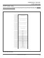
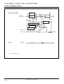
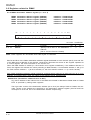
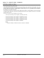
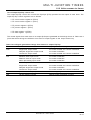
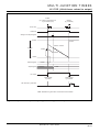
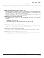
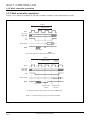
How to read internal I/O register tables
➀ Bit Numbers: Each register is connected with an internal bus of 16-bit
wide, so the bit numbers of the registers located at even
addresses are D0-D7, and those at odd addresses are
D8-D15.
➁ State of Register at Reset: Represents the initial state of each register
immediately after reset with hexadecimal numbers
(undefined bits after reset are indicated each in column ➂.)
➂ State of Bit at Reset: Represents the initial state of each bit immediately
after reset.
0... Zero immediately after reset
1... One immediately after reset
?... Undefined immediately after reset
○ ... read enabled
- ... read disabled (read value invalid)
0 ... Read always as 0
1 ... Read always as 1
At read:
➄ At write:
○ : Write enabled
△ : Write enable conditionally
(include some conditions at write)
- : Write disabled (Written value invalid)
<Example of representation>
Registers represented with thick rectangles
are accessible only with halfwords or words
(not accessible with bytes).
Not implemented
in the shaded portion.
D0
1 →
1
2
3
4
Abit
Bbit
Cbit
<at reset: H'04>
2
→
D
Bit name
0
Not assigned.
1
Abit
0: -----
(...................)
1: -----
Bbit
0: -----
(...................)
1: -----
Cbit
0: -----
(...................)
1: -----
2
3
Function
ini.
R
0
0
-
0
○
○
0
○
○
0
○
○
↑
↑
↑
3
4
5
W
Table of contents
Table of contents
CHAPTER 1 SUMMARY
1-1
1.1 Summary of M32150F4TFP ........................................................................................ 1-2
1.1.1 M32R family CPU ................................................................................................ 1-2
1.1.2 Multiply-accumulate operational function .......................................................... 1-3
1.1.3 Internal flash memory and RAM ........................................................................ 1-3
1.1.4 Clock frequency multiplier ................................................................................... 1-3
1.1.5 Versatile peripheral functions ............................................................................. 1-4
1.2 Block diagram .............................................................................................................. 1-6
1.3 Pin functions ................................................................................................................ 1-9
1.4 Pin assignment .......................................................................................................... 1-14
CHAPTER 2 CPU
2-1
2.1 CPU register ................................................................................................................. 2-2
2.2 General-purpose registers ......................................................................................... 2-2
2.3 Control registers .......................................................................................................... 2-3
2.3.1 Processor status word register: PSW (CR0) .................................................... 2-4
2.3.2 Condition bit register: CBR (CR1) ..................................................................... 2-5
2.3.3 Interrupt stack pointer: SPI (CR2) ..................................................................... 2-5
User stack pointer:SPU (CR3) ......................................................................... 2-5
2.3.4 Backup PC: BPC (CR6) ...................................................................................... 2-5
2.4 Accumulator .................................................................................................................. 2-6
2.5 Program counter .......................................................................................................... 2-6
2.6 Data format ................................................................................................................... 2-7
2.6.1 Data type ............................................................................................................... 2-7
2.6.2 Data format ........................................................................................................... 2-8
2.7 Notes on use of accumulator ................................................................................. 2-10
CHAPTER 3 ADDRESS SPACE
3-1
3.1 Summary of address space ...................................................................................... 3-2
3.2 Operation modes ......................................................................................................... 3-4
3.3 Internal ROM and expanded external area ............................................................ 3-5
3.3.1 Internal ROM area ............................................................................................... 3-5
3.3.2 Expanded external area ...................................................................................... 3-5
3.4 Internal RAM and SFR area ...................................................................................... 3-6
3.4.1 Internal RAM area ................................................................................................ 3-6
3.4.2 SFR (Special Function Register) area .............................................................. 3-6
3.5 EIT vector entry ......................................................................................................... 3-15
3.6 ICU vector table ......................................................................................................... 3-16
3.7 Notes on address space .......................................................................................... 3-17
M32150F4TFP User's Manual
i
Table of contents
CHAPTER 4 EIT
4-1
4.1 Summary of EIT ........................................................................................................... 4-2
4.2 EIT events of M32150F4TFP ..................................................................................... 4-3
4.2.1 Exception ............................................................................................................... 4-3
4.2.2 Interrupt ................................................................................................................. 4-3
4.2.3 Trap ........................................................................................................................ 4-3
4.3 EIT processing procedure ......................................................................................... 4-4
4.4 EIT processing mechanism ....................................................................................... 4-5
4.5 EIT event acceptance ................................................................................................. 4-6
4.6 Save and return of PC and PSW ............................................................................. 4-7
4.7 EIT vector entry ........................................................................................................... 4-9
4.8 Exception processing ............................................................................................... 4-10
4.8.1 Reserved instruction exception (RIE) .............................................................. 4-10
4.8.2 Address Exception (AE) .................................................................................... 4-12
4.9 Interrupt processing ................................................................................................. 4-14
4.9.1 Reset interrupt (RI) ............................................................................................ 4-14
4.9.2 System break interrupt (SBI) ............................................................................ 4-15
4.9.3 External interrupt (EI) ........................................................................................ 4-17
4.10 Trap processing ....................................................................................................... 4-19
4.10.1 Trap (TRAP) ..................................................................................................... 4-19
4.11 EIT priority ................................................................................................................ 4-21
4.12 EIT processing example ........................................................................................ 4-22
CHAPTER 5 INTERNAL MEMORY
5-1
5.1
5.2
5.3
5.4
Summary of internal memory ................................................................................... 5-2
Internal RAM ................................................................................................................. 5-2
Internal flash memory ................................................................................................ 5-2
Programming of internal flash memory ................................................................. 5-3
5.4.1 Outline of programming flash memory .............................................................. 5-3
5.4.2 Operation modes at programming flash memory ............................................ 5-6
5.4.3 RSIF (RAM Serial InterFace) ............................................................................. 5-7
5.4.4 Procedure of programming internal flash memory .......................................... 5-9
5.4.5 Time required to program flash memory ........................................................ 5-14
5.4.6 External protection circuit of VPP/MOD1 pins ............................................... 5-15
5.5 Registers related to internal flash memory ........................................................ 5-16
5.5.1 Flash mode register (FMOD) ............................................................................ 5-17
5.5.2 Flash control register (FCNT)........................................................................... 5-18
5.5.3 Block erase control register (FBLK) ................................................................ 5-19
5.6 Virtual flash emulation ............................................................................................. 5-20
5.6.1 Area available for virtual flash emulation ....................................................... 5-20
5.6.2 Entering virtual flash emulation mode ............................................................. 5-20
CHAPTER 6 RESET
6-1
6.1 Summary of reset ........................................................................................................ 6-2
6.2 Reset operation ............................................................................................................ 6-2
6.2.1 Reset at power on ............................................................................................... 6-2
6.2.2 Reset during operation ........................................................................................ 6-2
6.2.3 Reset vector at rewriting flash memory ............................................................ 6-2
6.3 Internal states immediately after leaving reset .................................................... 6-2
ii
M32150F4TFP User's Manual
Table of contents
CHAPTER 7 EXTERNAL BUS INTERFACE
7-1
7.1 Signals related to external bus interface .............................................................. 7-2
7.2 Read/write operations ................................................................................................. 7-4
7.3 Bus arbitration ............................................................................................................. 7-7
CHAPTER 8 I/O PORT AND PIN FUNCTION
8-1
8.1 Summary of I/O ports ................................................................................................. 8-2
8.2 Selection of pin function ........................................................................................... 8-3
8.3 Registers related to I/O ports .................................................................................. 8-5
8.3.1 Port data register ................................................................................................. 8-7
8.3.2 Port direction register .......................................................................................... 8-8
8.3.3 Port operation mode register .............................................................................. 8-9
8.4 Port peripheral circuit .............................................................................................. 8-19
CHAPTER 9 DMAC
9-1
9.1 Summary of DMAC ...................................................................................................... 9-2
9.2 Registers related to DMAC ....................................................................................... 9-4
9.2.1 DMAn channel control registers (n = 0 to 4) ................................................... 9-6
9.2.2 DMAn software request generate register (n = 0 to 4) ................................ 9-12
9.2.3 DMAn source address register (n = 0 to 4) .................................................. 9-13
9.2.4 DMAn destination address register (n = 0 to 4) ........................................... 9-14
9.2.5 DMAn transfer count register (n = 0 to 4) ..................................................... 9-15
9.2.6 DMA interrupt request status register (DMITST) ........................................... 9-16
9.2.7 DMA interrupt mask register (DMITMK) .......................................................... 9-17
9.3 Functional description of DMAC ............................................................................ 9-18
9.3.1 DMA request sources ........................................................................................ 9-18
9.3.2 Sequences of DMA transfer processing ......................................................... 9-20
9.3.3 Start of DMA ....................................................................................................... 9-21
9.3.4 Channel priority levels ....................................................................................... 9-21
9.3.5 Holding and relinquishing of internal bus ....................................................... 9-21
9.3.6 Unit of transfer ................................................................................................... 9-21
9.3.7 Number of transfers ........................................................................................... 9-21
9.3.8 Address space .................................................................................................... 9-22
9.3.9 Transfer operation .............................................................................................. 9-22
9.3.10 DMA completion and interrupts .................................................................... 9-25
9.3.11 States of registers after DMA transfer complete ......................................... 9-25
9.4 Notes on use of DMAC ............................................................................................ 9-26
CHAPTER 10 MULTI-JUNCTION TIMERS
10-1
10.1 Summary of multi-junction timers ....................................................................... 10-2
10.2 Units common to timers ........................................................................................ 10-6
10.2.1 Register map related to units common to the timers ................................. 10-6
10.2.2 Prescalers ......................................................................................................... 10-8
10.2.3 Clock bus/input and output event bus control unit ..................................... 10-9
10.2.4 Input processing control unit ........................................................................ 10-14
10.2.5 Output flip-flop control unit ........................................................................... 10-21
10.2.6 Interrupt control unit ...................................................................................... 10-28
M32150F4TFP User's Manual
iii
Table of contents
10.3 TOP (16-bit timers related to output) ............................................................... 10-39
10.3.1 Summary of TOPs ......................................................................................... 10-39
10.3.2 Outline of TOP modes .................................................................................. 10-41
10.3.3 Register map related to TOPs ..................................................................... 10-42
10.3.4 TOP control registers .................................................................................... 10-45
10.3.5 TOP counters (TOP0CT to TOP10CT) ....................................................... 10-52
10.3.6 TOP reload registers (TOP0RL to TOP10RL) ........................................... 10-53
10.3.7 TOP adjust registers (TOP0CC to TOP10CC) ........................................... 10-54
10.3.8 TOP0 to TOP10 external enable permit register (TOPEEN) ................... 10-55
10.3.9 TOP0 to TOP10 enable protect register (TOPPRO) ................................. 10-56
10.3.10 TOP0 to TOP10 count enable register (TOPCEN) ................................. 10-57
10.3.11 Operation of TOP single-shot output mode (with adjust function) ....... 10-58
10.3.12 Operation of TOP delayed single-shot output mode
(with adjust function) ................................................................................ 10-64
10.3.13 Operation of TOP continuous output mode
(without adjust function) ........................................................................... 10-69
10.4 TIO (16-bit timers related to input/output) ...................................................... 10-72
10.4.1 Summary of TIOs ........................................................................................... 10-72
10.4.2 Outline of TIO modes .................................................................................... 10-74
10.4.3 Register map related to TIO ........................................................................ 10-76
10.4.4 TIO control registers ...................................................................................... 10-79
10.4.5 TIO counters (TIO0CT to TIO9CT) .............................................................. 10-90
10.4.6 TIO reload 0/measure register (TIO0RL0 to TIO9RL0) ............................ 10-91
10.4.7 TIO reload 1 registers (TIO0RL1 to TIO9RL1) .......................................... 10-92
10.4.8 TIO0 to TIO9 enable protect register (TIOPRO) ....................................... 10-93
10.4.9 TIO0 to TIO9 count enable register (TIOCEN).......................................... 10-94
10.4.10 Operation of TIO measure (free-run/clear) input mode .......................... 10-95
10.4.11 Operation of TIO noise processing input mode ...................................... 10-98
10.4.12 Operation of TIO PWM output mode ........................................................ 10-99
10.4.13 Operation of TIO single-shot output mode (without adjust function) .. 10-103
10.4.14 Operation of TIO single-shot output mode (without adjust function) . 10-105
10.4.15 Operation of TIO continuous output mode (without adjust function) .. 10-107
10.5 TMS (16-bit timers related to input) ............................................................... 10-109
10.5.1 Summary of TMSs ....................................................................................... 10-109
10.5.2. Summary of TMS Operation ...................................................................... 10-109
10.5.3 Register map related to TMS ..................................................................... 10-111
10.5.4 TMS control registers .................................................................................. 10-112
10.5.5 TMS counters (TMS0CT, TMS1CT) .......................................................... 10-114
10.5.6 TMS measure register
(TMS0MR3 to TMS0MR0, TMS1MR3 to TMS1MR0) ............................ 10-115
10.5.7 Operation of TMS measure inputs ............................................................ 10-116
10.6 TML(32-bit timers related to input) ................................................................. 10-118
10.6.1 Summary of TMLs........................................................................................ 10-118
10.6.2 Summary of TML operation ........................................................................ 10-119
10.6.3 Register map related to TML registers ..................................................... 10-120
10.6.4 TML control register (TMLCR) ................................................................... 10-121
10.6.5 TML counter (TMLCTH, TMLCTL) ............................................................. 10-122
10.6.6 TML measure registers
(TMLMR3H to TMLMR0H, TMLMR3L to TMLMR0L) ............................ 10-123
10.6.7 Operation of TML measure inputs ............................................................. 10-124
iv
M32150F4TFP User's Manual
Table of contents
CHAPTER 11 A-D CONVERTER
11-1
11.1 Summary of A-D converter .................................................................................. 11-2
11.1.1 Conversion modes ........................................................................................... 11-5
11.1.2 Operation modes .............................................................................................. 11-6
11.1.3 Special operation modes ............................................................................... 11-10
11.1.4 A-D conversion interrupt request and DMA transfer request .................. 11-13
11.2 Registers related to A-D converter ................................................................... 11-14
11.2.1 Single mode register 0 (ADSIM0) ................................................................ 11-15
11.2.2 Single mode register 1 (ADSIM1) ................................................................ 11-17
11.2.3 Scan mode register 0 (ADSCM0) ................................................................ 11-19
11.2.4 Scan mode register 1 (ADSCM1) ................................................................ 11-21
11.2.5 A-D successive approximation register (ADSAR) ...................................... 11-23
11.2.6 A-D comparate data register (DCMP) ......................................................... 11-24
11.2.7 A-D data register 0 to A-D data register 15 (ADDT0 to ADDT15) ........ 11-25
11.3 Functional description of A-D converter ......................................................... 11-26
11.3.1 Analog input voltage ...................................................................................... 11-26
11.3.2 Successive-approximation A-D conversion ................................................. 11-27
11.3.3 Comparator operation .................................................................................... 11-29
11.3.4 Calculation of A-D conversion time ............................................................. 11-30
11.3.5 Accuracy of A-D conversion ......................................................................... 11-32
11.4 Notes on use of A-D converter .......................................................................... 11-34
CHAPTER 12 SERIAL I/O
12-1
12.1 Summary of serial I/O ............................................................................................ 12-2
12.2 Registers related to serial I/O .............................................................................. 12-4
12.2.1 SIOn mode register (n = 0, 1) ....................................................................... 12-5
12.2.2 SIOn control register 0 (n = 0, 1) ................................................................. 12-8
12.2.3 SIOn control register 1 (n = 0, 1) ............................................................... 12-10
12.2.4 SIOn baud rate register (n = 0, 1) .............................................................. 12-11
12.2.5 SIOn interrupt mask register (n = 0, 1) ...................................................... 12-12
12.2.6 SIOn status register (n = 0, 1) .................................................................... 12-14
12.2.7 SIOn transmit buffer register (n = 0, 1) ..................................................... 12-17
12.2.8 SIOn receive buffer register (n = 0, 1)....................................................... 12-18
12.3 Transmission in CSIO mode ............................................................................... 12-19
12.3.1 Setting of CSIO baud rate ............................................................................ 12-19
12.3.2 Initialization at CSIO transmission ............................................................... 12-20
12.3.3 Beginning of CSIO transmission .................................................................. 12-22
12.3.4 CSIO continuous transmission ..................................................................... 12-22
12.3.5 CSIO transmit complete processing ............................................................ 12-22
12.3.6 CSIO transmit operation ................................................................................ 12-24
12.4 Reception in CSIO mode ..................................................................................... 12-26
12.4.1 Initialization at CSIO reception .................................................................... 12-26
12.4.2 Beginning of CSIO reception ........................................................................ 12-28
12.4.3 CSIO receive complete processing ............................................................. 12-28
12.4.4 Flags indicating states of CSIO receive operation .................................... 12-30
12.4.5 CSIO receive operation ................................................................................. 12-31
12.5 Notes on use of CSIO mode .............................................................................. 12-33
12.6 Transmission in UART mode .............................................................................. 12-35
12.6.1 Setting of URAT baud rate ........................................................................... 12-35
12.6.2 UART transmit/receive data formats ........................................................... 12-36
M32150F4TFP User's Manual
v
Table of contents
12.6.3 Initialization at UART transmission .............................................................. 12-38
12.6.4 Beginning of UART transmission ................................................................. 12-40
12.6.5 UART continuous transmission .................................................................... 12-40
12.6.6 UART transmit complete processing ........................................................... 12-40
12.6.7 UART transmit operation............................................................................... 12-42
12.7 Reception in UART mode .................................................................................... 12-44
12.7.1 Initialization at UART reception ................................................................... 12-44
12.7.2 Beginning of UART reception ....................................................................... 12-46
12.7.3 UART receive complete processing ............................................................ 12-46
12.7.4 UART receive operation ................................................................................ 12-48
12.8 Notes on use of UART mode ............................................................................. 12-51
CHAPTER 13 INTERRUPT CONTROLLER
13-1
13.1 Summary of interrupt controller (ICU) ............................................................... 13-2
13.2 Interrupt sources of internal peripheral I/Os .................................................... 13-4
13.3 Registers related to ICU ........................................................................................ 13-5
13.3.1 Interrupt vector register (IVECT) ................................................................... 13-6
13.3.2 Interrupt mask register (IMASK) .................................................................... 13-7
13.3.3 SBI control register (SBICR) .......................................................................... 13-8
13.3.4 Interrupt control register .................................................................................. 13-9
13.4 ICU vector table ..................................................................................................... 13-12
13.5 Interrupt operation ................................................................................................ 13-15
13.5.1 Acceptance of interrupts from internal peripheral I/Os ............................. 13-15
13.5.2 Interrupt handler processing of internal peripheral I/Os ........................... 13-17
13.6 System break interrupt (SBI) .............................................................................. 13-19
13.6.1 Acceptance of SBI ......................................................................................... 13-19
13.6.2 Handler processing of SBI ............................................................................ 13-19
CHAPTER 14 WAIT CONTROLLER
14-1
14.1 Summary of wait controller .................................................................................. 14-2
14.2 Registers related to wait controller .................................................................... 14-4
14.2.1 Wait cycle control register (WTCCR) ............................................................ 14-5
14.3 Wait controller operation ....................................................................................... 14-6
CHAPTER 15 REAL-TIME DEBUGGER
15.1 Summary of real-time debugger (RTD) .............................................................. 15-2
15.2 RTD pin functions ................................................................................................. 15-3
15.3 RTD operation ......................................................................................................... 15-4
15.3.1 Summary of RTD operation ............................................................................ 15-4
15.3.2 Operation of real-time output of RAM contents (RDR) .............................. 15-5
15.3.3 Operation of forced rewrite of RAM contents (WRR) ................................. 15-7
15.3.4 Continuous monitor operation (VER)............................................................. 15-9
15.3.5 Operation of return from runaway (RCV) ................................................... 15-10
15.3.6 Reset of RTD ................................................................................................. 15-11
15.4 Connection to host computer ............................................................................ 15-12
vi
M32150F4TFP User's Manual
15-1
Table of contents
CHAPTER 16 RAM BACKUP MODE
16-1
16.1 Summary .................................................................................................................... 16-2
16.2 An example of RAM backup at the time of power shutoff ........................... 16-3
16.2.1 The normal state of operation........................................................................ 16-4
16.2.2 The state at the time of RAM backup .......................................................... 16-5
16.3 An example of RAM backup for low power consumption ............................ 16-6
16.3.1 The normal state of operation........................................................................ 16-7
16.3.2 The state at the time of RAM backup mode ............................................... 16-8
16.3.3 Notes turning the power on ............................................................................ 16-9
16.4 Canceling RAM backup mode (wakeup) .......................................................... 16-10
CHAPTER 17 OSCILLATION CIRCUIT
17-1
17.1 Oscillation circuit .................................................................................................... 17-2
17.1.1 An example of oscillation circuit .................................................................... 17-2
17.1.2 Output function of the system clock ............................................................. 17-3
17.1.3 Oscillation stabilization time when the power is turned on ....................... 17-4
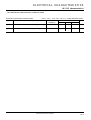
CHAPTER 18 ELECTRICAL CHARACTERISTICS
18-1
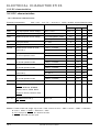
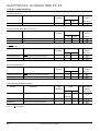
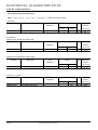
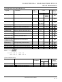
18.1 Absolute maximum ratings ................................................................................... 18-2
18.2 Recommended operating conditions .................................................................. 18-3
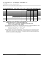
18.3 DC characteristics ................................................................................................... 18-4
18.3.1 Electrical characteristics .................................................................................. 18-4
18.3.2 Electrical characteristics related to flash ...................................................... 18-5
18.4 A-D conversion characteristics ............................................................................ 18-6
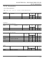
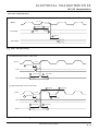
18.5 AC characteristics ................................................................................................... 18-7
18.5.1 Timing requirements ........................................................................................ 18-7
18.5.2 Switching characteristics ............................................................................... 18-10
18.5.3 AC characteristics .......................................................................................... 18-13
CHAPTER 19 STANDARD CHARACTRISTICS
17-1
19.1 A-D conversion charactristics .............................................................................. 17-2
APPENDIX 1 MECHANICAL SPECIFICATION
A1-1
A1.1 Package outline (Real chip) ................................................................................ A1-2
APPENDIX 2 INSTRUCTION PROCESSING TIME
A2-1
A2.1 Instruction processing time ................................................................................ A2-2
M32150F4TFP User's Manual
vii
Table of contents
viii
M32150F4TFP User's Manual
CHAPTER 1
SUMMARY
1.1
1.2
1.3
1.4
Summary of M32150F4TFP
Block diagram
Pin functions
Pin assignment
SUMMARY
1.1 Summary of M32150F4TFP
1.1 Summary of M32150F4TFP
1.1.1 M32R family CPU
(1) RISC architecture
The M32150F4TFP is a single-chip 32-bit RISC microcomputer provided with the M32R family CPU
(hereafter called the M32R CPU), a 128K-byte flash memory, a 6K-byte RAM, and integrated peripherals.
The M32R CPU is designed using RISC architecture with 83 instructions. The CPU accesses memory
with load and store instructions and performs various operations with register-to-register operation
instructions. It has sixteen 32-bit general-purpose registers.
The M32R CPU supports such compound instructions as load & address update, store & address
update, etc. in addition to ordinary load and store instructions. Compound instructions are effective
in high-speed data transfer.
(2) Five-stage pipeline processing
The M32R CPU executes instructions through the pipeline processing of 5 stages, i.e. the instruction
fetch, decode, execution, memory access, and write back stages. The CPU can execute the abovementioned compound instructions in one cycle as well as load, store, and register-to-register operation
instructions.
Instructions are sent to the execution stage in order of fetch. However, if the execution of the load
or store instruction that has been sent to this stage is retarded by the insertion of wait cycles for
memory access, the succeeding register-to-register operation instruction may take precedence to be
executed. This "out-of-order-completion" incorporated into the M32R CPU can make efficient use of
clock cycles for instruction execution.
(3) Compact instruction codes
The M32R CPU has two types of instructions in length, 16-bit and 32-bit wide. 16-bit instructions can
be effectively used to reduce the code size of program.
On the other hand, 32-bit instructions contain the instructions that can directly branch to an address
within the range of –32M bytes from that of each instruction under execution. The use of these
instructions allow easier programming than in the architecture with segmented address space.
1-2
M32150F4TFP User's Manual
SUMMARY
1.1 Summary of M32150F4TFP
1.1.2 Multiply-accumulate operational function
(1) High-speed multiplier
The M32R CPU is equipped with a 32-bit x 16-bit on-chip high-speed multiplier, which can executes
a multiply instruction of 32-bit by 32-bit integer multiplication in 3 cycles (40 ns per one cycle at 25
MHz internal operation).
(2) Multiply-accumulate operational function comparable to DSP
The M32R CPU supports the following four multiply functions of multiply-accumulate operation instructions
by using the 56-bit accumulator.
Either of these functions can be accomplished in one cycle.
•
•
•
•
the
the
the
the
high-order 16 bits of a register x the high-order 16 bits of another register
low order 16 bits of a register x the low-order 16 bits of another register
whole 32 bits of a register x the high-order 16 bits of another register
whole 32 bits of a register x the low-order 16 bits of another register
The M32R CPU provides such instruction as rounds the value stored in the accumulator to 16 or 32
bits or as stores the accumulator value in a register by shifting it for address alignment. Because the
M32R CPU can execute these instructions in one cycle, it accomplishes the data processing capability
compared to DSP by making use of these instructions together with high-speed data transfer instructions,
i.e. load & address update and store & address update.
1.1.3 Internal flash memory and RAM
The M32150F4TFP provides a 128K-byte flash memory and a 6K-byte RAM accessible with no wait,
which are useful for configuring embedded high-speed systems.
The internal flash memory can be programmed in the same condition as it will be connected to the
final printed circuit board (on-board programming). Thus, by using the flash memory, the chips used
in prototype design will be brought into production as they are, as well as the PC board will be
without any modification.
The internal flash memory is provided with virtual flash emulation function, so the internal RAM can
be mapped virtually into a portion of the flash memory. This function together with the on-chip realtime debugger (RTD) facilitates data tuning on the ROM table.
By using the RTD, the internal RAM can externally be read or rewritten independently of the M32R
CPU. The RAM communicates with the external circuit through the synchronous serial I/O dedicated
to the RTD.
1.1.4 Clock frequency multiplier
The M32150F4TFP internally doubles the input clock frequency to make the internal clock. A 12.5
MHz input clock frequency, for example, generates an internal clock of 25 MHz.
M32150F4TFP User's Manual
1-3
SUMMARY
1.1 Summary of M32150F4TFP
1.1.5 Versatile peripheral functions
(1) Multi-junction timers (MJTs)
The multi-junction timers consist of 33 channels in total, including 11 channels of the output-related
timers, 10 channels of the input/output-related timers, 8 channels of the 16-bit input-related timers,
and 4 channels of the 32-bit input-related timers. Many of these timers operate in two or more
modes, which are selectable for various applications.
The multi-junction timers are provided with a clock bus, an input event bus, and an output event bus,
with which they can be internally connected to each other as well as used as individual timers. This
function provides flexible timer configuration and capability for various applications.
The output-related timers have adjust function, which increments or decrements count values freely
during count operation, resulting in real-time control.
(2) Direct memory access controller (DMAC)
The on-chip 5-channel DMAC supports direct data transfer between internal peripheral I/Os, between
internal peripheral I/O and internal RAM, and between internal RAMs. DMA transfer requests can be
triggered with user-programmable software or signals generated by internal peripheral I/Os (A-D
converter, MJTs, and serial I/O).
Because DMA channels can be connected in cascade, the completion of the DMA transfer of a
channel starts the DMA transfer of another channel. This function facilitates high-functional DMA
transfer operation without any CPU service overhead.
(3) A-D converter
The 16-channel A-D converter has a resolution of 10 bits. The converter performs A-D conversion
of 4 channels, 8 channels or 16 channels as a group as well as of each individual channel.
The A-D converter supports the comparate mode in which the converter compares a result of A-D
conversion with the specified value and determine which is larger.
When A-D conversion is completed, an A-D conversion complete interrupt or a DMA transfer request
can be generated.
(4) High-speed serial I/O
The M32150F4TFP provides 2 channels of serial I/O, used as synchronous I/O or UART.
Data can be transferred at a maximum transfer rate of 2 Mbps in synchronous I/O (at 25 MHz internal
operation).
When a data reception completed or a transmit buffer register emptied, the SIO channels can generate
DMA transfer requests.
(5) Real-time debugger (RTD)
The on-chip real-time debugger (RTD) provides the facility in accessing the internal RAM directly
from the external circuit. The RAM communicates with the external circuit through the synchronous
serial I/O dedicated to the RTD.
By using the RTD, the internal RAM can externally be read or rewritten independently of the M32R
CPU.
1-4
M32150F4TFP User's Manual
SUMMARY
1.1 Summary of M32150F4TFP
(6) Interrupt controller
The interrupt controller defines eight interrupt priority levels including interrupt disable, with which it
manages the interrupt requests from internal peripheral I/Os. It also accepts system break interrupts
generated by any fault in power supply or by the external watchdog timer.
(7) Three operating modes
The M32150F4TFP has three operation modes, the single chip, the expanded external, and the
processor mode. Each mode, having its own address space and external pin functions, is selected
by the MOD0 and MOD1 mode definition pins.
(8) Wait controller
The wait controller supports accessing the expanded external area. The maximum of 1M bytes is
assigned to this area in every mode except the single chip mode.
M32150F4TFP User's Manual
1-5
SUMMARY
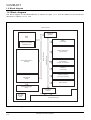
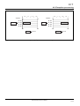
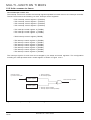
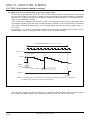
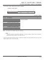
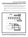
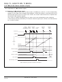
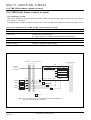
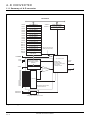
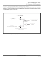
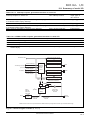
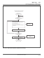
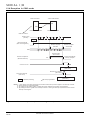
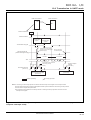
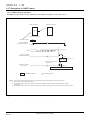
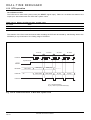
1.2 Block diagram
1.2 Block diagram
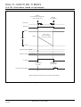
The block diagram of the M32150F4TFP is shown in Figure 1.2.1, and the features of its blocks are
described in Tables 1.2.1 to 1.2.3.
M32150F4TFP
Internal bus
interface
M32R
CPU
DMAC
(5 channels)
Internal flash memory
(128 KB)
Multi-junction timers
(33 channels)
Internal 16-bit bus
Internal 32-bit bus
Multiply-accumulate
operational unit
A-D converter
(10 bits, 16 channels)
Serial I/O
( 2 channels)
Interrupt controller
(19 sources 8 levels)
Internal RAM
(6 KB)
Wait controller
Real-time debugger
(RTD)
External bus
interface
Data
PLL clock
generation
circuit
Address
I/O ports (total 109)
Fig. 1.2.1 Block diagram of M32150F4TFP
1-6
M32150F4TFP User's Manual
SUMMARY
1.2 Block diagram
Table 1.2.1 M32R family CPU
Functional block
Features
M32R family CPU
• Bus specification
Basic bus cycle: 40 ns (at 25 MHz internal operation)
Logical address space: 4G bytes linear
Expanded external area: 1M bytes maximum
External data bus: 16 bits wide
• Implementation: 5-stage pipeline architecture
• CPU core: internal 32 bits
• Registers
General-purpose registers: 32 bits x 16
Control registers: 32 bits x 5
• Instruction set
16-bit/32-bit instructions
83 instructions with 9 addressing modes
• On-chip multiply-accumulate operational unit
Table 1.2.2 Internal memory
Functional block
Features
RAM
• Size: 6K bytes
• No wait access (at 25 MHz internal operation)
• RAM can externally be read or rewritten independently of M32R CPU using RTD
(real-time debugger)
Flash memory
• Size: 128K bytes
• No wait access (at 25 MHz internal operation)
• Programming function available using dedicated serial I/O (RSIF)
M32150F4TFP User's Manual
1-7
SUMMARY
1.2 Block diagram
Table 1.2.3 Internal peripheral I/Os
Functional block
Features
DMAC
• 5 channels
• Supports DMA transfer between internal peripheral I/Os, between internal RAM
and internal peripheral I/Os, and between internal RAMs
• High-functional DMA transfer by combining request source from internal peripheral
I/Os
• Cascade connection between DMAC channels available (completion of transfer of
a channel starts transfer of another channel).
Multi-junction timers
• 33 channels of multifunctional timers
• 11 channels of output-related timers, 10 channels of input/output-related timers,
8 channels of 16-bit input-related timers, and 4 channels of 32-bit input-related
timers
• Flexible timer configuration available by interconnecting channels
A-D converter
• 16 channels of 10-bit resolution
• Comparator mode available
• Interrupt or DMA transfer can be generated at A-D conversion completion
Serial I/O
• 2 channels
• Synchronous serial I/O or UART selectable
• High-speed data transfer: 2 Mbps at synchronous serial I/O and 195 Kbps at
UART
Real-time debugger
• CPU-independent rewriting and monitoring of internal RAM by externally input
commands
• Equipped with dedicated synchronous serial port
Interrupt controller
• Controls interrupt requests from internal peripheral I/Os
• 8 priority levels including interrupt disable
Wait controller
• Controls wait cycles for accessing expanded external area
• Software-programmable 1- to 4-wait insertion + arbitrary wait insertion by external
_____
WAIT signal input
Clock PLL
• Multiply-by-two clock generator
(an input clock of 12.5 MHz at 25 MHz internal operation)
1-8
M32150F4TFP User's Manual
SUMMARY
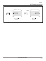
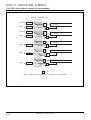
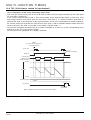
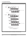
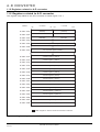
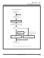
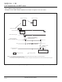
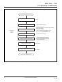
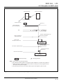
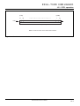
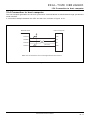
1.3 Pin functions
1.3 Pin functions
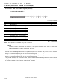
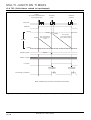
The pin functional diagram is shown in Figure 1.3.1 and the pin descriptions are explained in Table 1.3.1.
Clock
Port 7
XIN
CS1/P45
XOUT
CS0/P44
VCNT
RD/P43
OSC-VCC
BHW/P42
OSC-VSS
BLW/P41
Port 4
Bus
control
WAIT/P71
BCLK /P70
HREQ/P72
Reset
Port 7
HACK/P73
RESET
18
MOD0
Mode
MOD1
Port 15
Port 14
Port 13
/P150 to P157,
P140 to P147,
P130 to P137
4
Port 12
Multi-junction
timers
TCLK 0 to TCLK 3
/P124 to P127
DB0 to DB15
/P00 to P07,
P10 to P17
Data
bus
Port 2
Port 3
Port 4
Port 0
Port 1
TXD0/RTX/P82
RXD0/RRX/P83
SCLKI 0/SCLKO 0
/P84
21
TO 0 to TO 20
/P110 to P117,
P100 to P107,
P93 to P97
Port 11
Port 10
Port 9
Address
bus
16
M32150F4TFP
24
TIN 0 to TIN 23
A13 to A30
/P20 to P27,
P30 to P37,
P47, P46
TXD1/P85
Serial
I/O
Port 8
RXD1/P86
SCLKI 1/SCLKO 1
/P87
16
AN0 to AN15
Port 6
A-D
converter
ADSEL0/P65
RTDTXD/P74
ADSEL1/P66
RTDRXD/P75
ADTRG/P67
RTDACK/P76
AVCC
RTDCLK/P77
Real-time
debugger
Port 7
AVSS
AVREF
SBI/P64
Port 6
Interrupt
controller
Port 6
P61 to P63
VDD
VPP
11
VCC
11
VSS
Fig. 1.3.1 Pin functions diagram
M32150F4TFP User's Manual
1-9
SUMMARY
1.3 Pin functions
Table 1.3.1 Pin function descriptions (1/4)
Type
Symbols
Name
Input/
Function
Output
Power
VCC
Power source
-
All VCC pins should be connected on a VCC plane
source
VDD
RAM power source
-
Power source for internal RAM backup
VPP
FLASH power source
-
Power source for on-chip flash memory programming/
erasure system
VSS
System ground
-
All VSS pins should be connected on a ground plane
(GND)
Clock
XIN,
Clock
XOUT
Input
Clock input and output: clock of one-half the operation
Output
frequency is input to PLL clock frequency multiplier
(XIN input = 12.5 MHz at 25 MHz internal operation)
BCLK
System clock
Output
Outputs the clock of twice the input clock frequency
(BCLK output = 25 MHz at 25 MHz internal operation):
used to design synchronous external circuits
OSC-VCC,
Power source
-
Power source to PLL circuit: OSC-VCC connected
OSC-VSS
Ground
-
to power source and OSC-VSS to ground
VCNT
PLL control
Input
Control for PLL circuit: a resistor and a capacitor
are connected.
For external circuit, refer to Section 17.1.1 "An
example of oscillation circuit".
Reset
RESET
Reset
Input
Internal reset
Mode
MOD0,
Mode
Input
Define operation mode
MOD1
Address A13 to A30
Address bus
Output
bus
MOD0
MOD1
Mode
0
0
Single chip mode
0
1
Expanded external mode
1
0
Processor mode
1
1
(Reserved)
Used to connect two off-chip memory spaces of
maximum 4M bits(512K bytes) each if necessary
(A31 notoutputted). Byte position in 16-bit data bus
to whichvalid data is written is indicated by a BHW
or BLW output during write cycle. 16-bit data bus is
always read during read cycle; however, only data
at valid byte position is transferred to M32150F4TFP
internal circuitry.
Data
DB0 to DB15 Data bus
I/O
16-bit data bus connected to external devices
bus
1-10
M32150F4TFP User's Manual
SUMMARY
1.3 Pin functions
Table 1.3.1 Pin function descriptions (2/4)
Type
Symbols
Name
Input/
Function
Output
Bus
CS0,
control
CS1
Chip select
Output
Chip select signal for accessing external devices;
for the expanded external area accessible by each
chip select signal, refer to Chapter 3 "Address
space"
RD
Read
Output
Outputted at a read of external device
BHW
Byte high write
Output
Indicate byte positions to which valid data is
transferred at a write of external device; BHW
BLW
Byte low write
corresponds to the high-order address (DB0 to DB7
valid), and BLW to the low-order address (DB8 to
DB15 valid)
WAIT
Wait
Input
If tied "L", wait cycles are extended when
M32150F4TFP accesses external device
HREQ
Hold request
Input
Used for external devices to request bus hold of
external bus; if tied "L", M32150F4TFP goes to
the hold state
HACK
Hold acknowledges
Output
M32150F4TFP goes to the hold state, relinquishing
the bus of the external bus
Multi-
TIN0 to
junction
TIN23
Timer input
Input
Input pins to multi-junction timers
Timer output
Output
Output pins from multi-junction timers
Input
Clock input pins to multi-junction timers
-
Power source to A-D converter; AVCC connected
timers
TO0 to
TO20
TCLK0 to Timer clock
TCLK3
A-D
AVCC,
Analog power source
converter
to VCC
AVSS
Analog ground
-
AVSS connected to ground
AN0 to
Analog input
Input
16-channel analog inputs of A-D converter
AVREF
Reference voltage input
Input
Reference voltage input of A-D converter
ADTRG
Converted trigger
Input
Hardware trigger input for starting A-D conversion
Output
Analog switch pins connected to external devices,
AN15
ADSEL0, Analog selector
ADSEL1
used to extend the number of input pins of A-D
converter
Interrupt SBI
controller
System break interrupt
Input
System break interrupt (SBI) input of interrupt
controller
M32150F4TFP User's Manual
1-11
SUMMARY
1.3 Pin functions
Table 1.3.1 Pin function descriptions (3/4)
Type
Symbols
Name
Input/
output
Function
Serial
TXD0
Transmit data
Output
Output of serial I/O channel 0
I/O
RXD0
Receive data
Input
Input of serial I/O channel 0
SCLKI 0/
UART transmit/
I/O
Channel 0 in UART mode:
SCLKO 0
receive clock input
Transmit/receive clock input when external clock
or
selected
CSIO transmit/
Channel 0 in CSIO mode:
receive clock
Transmit/receive clock input when external
input/output
clock selected
Transmit/receive clock output when internal
clock selected
TXD1
Transmit data
Output
Transmit data output of serial I/O channel 1
RXD1
Receive data
Input
Receive data input of serial I/O channel 1
SCLKI 1/
UART transmit/
I/O
Channel 1 in UART mode:
SCLKO 1
receive clock input
Transmit/receive clock input when external clock
or
selected
CSIO transmit/
Channel 1 in CSIO mode:
receive clock
Transmit/receive clock input when external
input/output
clock selected
Transmit/receive clock output when internal
clock selected
Real-time
RTDTXD
Transmit data
Output
Serial data output of real-time debugger
Debugger
RTDRXD
Receive data
Input
Serial data input of real-time debugger
RTDCLK
Clock input
Input
Serial data transmit/receive clock input of real-time
debugger
RTDACK
Aknowledge
Output
Outputs "L" pulse synchronized to the beginning
clock of serial output data word of real-time debugger;
"L" width of the pulse indicatesthe kind of command
or data that real-time debugger received
Serial I/O
RRX
RSIF receive
Input
Transmit/receive pins of serial I/O (RSIF: RAM Serial
dedicated
RTX
RSIF transmit
Output
InterFace) dedicated to transfer program used for
to flash
writing to flash memory; refer to Section 5.5
memory
"Programming of internal flash memory" for detail
1-12
M32150F4TFP User's Manual
SUMMARY
1.3 Pin functions
Table 1.3.1 Pin function descriptions (4/4)
Type
Symbols
Name
Input/
Function
output
I/O
P00 to P07
I/O port0
I/O
Programmable I/O port pins
ports
P10 to P17
I/O port1
I/O
Programmable I/O port pins
(see
P20 to P27
I/O port2
I/O
Programmable I/O port pins
P30 to P37
I/O port3
I/O
Programmable I/O port pins
P41 to P47
I/O port4
I/O
Programmable I/O port pins
P61 to P67
I/O port6
I/O
Programmable I/O port pins except P64
note)
(P64 is SBI input-only port)
P70 to P77
I/O port7
I/O
Programmable I/O port pins
P82 to P87
I/O port8
I/O
Programmable I/O port pins
P93 to P97
I/O port9
I/O
Programmable I/O port pins
P100 to P107
I/O port10
I/O
Programmable I/O port pins
P110 to P117
I/O port11
I/O
Programmable I/O port pins
P124 to P127
I/O port12
I/O
Programmable I/O port pins
P130 to P137
I/O port13
I/O
Programmable I/O port pins
P140 to P147
I/O port14
I/O
Programmable I/O port pins
P150 to P157
I/O port15
I/O
Programmable I/O port pins
Note: I/O port 5 is MITSUBISHI reserved.
M32150F4TFP User's Manual
1-13
SUMMARY
1.4 Pin assignment
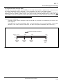
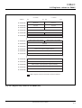
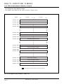
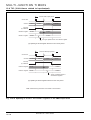
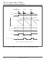
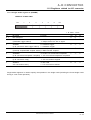
1.4 Pin assignment
120
119
118
117
116
115
114
113
112
111
110
109
108
107
106
105
104
103
102
101
100
99
98
97
96
95
94
93
92
91
90
89
88
87
86
85
84
83
82
81
VSS
P113/TO3
P112/TO2
P111/TO1
P110/TO0
P127/TCLK3
P126/TCLK2
P125/TCLK1
P124/TCLK0
P137/TIN23
P136/TIN22
P135/TIN21
P134/TIN20
P133/TIN19
P132/TIN18
P131/TIN17
P130/TIN16
P147/TIN15
P146/TIN14
P145/TIN13
P144/TIN12
P143/TIN11
P142/TIN10
P141/TIN9
P140/TIN8
VCC
VSS
P157/TIN7
P156/TIN6
P155/TIN5
P154/TIN4
P153/TIN3
P152/TIN2
P151/TIN1
P150/TIN0
P27/A30
P26/A29
P25/A28
P24/A27
VCC
The pin assingnment of the M32150F4TFP is shown in Figure 1.4.1, and the M32150F4TFP pin names with
package location is shown in Table 1.4.1.
121
122
123
124
125
126
127
128
129
130
131
132
133
134
135
136
137
138
139
140
141
142
143
144
145
146
147
148
149
150
151
152
153
154
155
156
157
158
159
160
M32150F4TFP
160 pins QFP/0.65 mm pitches
VCC
P61
P62
P63
P64/SBI
P65/ADSEL0
P66/ADSEL1
P67/ADTRG
P70/BCLK
P71/WAIT
P72/HREQ
P73/HACK
P74/RTDTXD
P75/RTDRXD
P76/RTDACK
P77/RTDCLK
VSS
VCC
VDD
P82/TXD0/RTX
P83/RXD0/RRX
P84/SCLKI0/SCLKO0
P85/TXD1
P86/RXD1
P87/SCLKI1/SCLKO1
VSS
OSC-VSS
XIN
XOUT
OSC-VCC
VCNT
VCC
RESET
MOD0
MOD1
VPP
P00/DB0
P01/DB1
P02/DB2
VSS
1
2
3
4
5
6
7
8
9
10
11
12
13
14
15
16
17
18
19
20
21
22
23
24
25
26
27
28
29
30
31
32
33
34
35
36
37
38
39
40
VCC
P114/TO4
P115/TO5
P116/TO6
P117/TO7
P100/TO8
P101/TO9
P102/TO10
P103/TO11
P104/TO12
P105/TO13
P106/TO14
P107/TO15
P93/TO16
P94/TO17
P95/TO18
P96/TO19
P97/TO20
VSS
VCC
AVREF
AVCC
AN0
AN1
AN2
AN3
AN4
AN5
AN6
AN7
AN8
AN9
AN10
AN11
AN12
AN13
AN14
AN15
AVSS
VSS
Fig. 1.4.1 Pin assignment
1-14
M32150F4TFP User's Manual
80
79
78
77
76
75
74
73
72
71
70
69
68
67
66
65
64
63
62
61
60
59
58
57
56
55
54
53
52
51
50
49
48
47
46
45
44
43
42
41
VSS
P23/A26
P22/A25
P21/A24
P20/A23
P37/A22
P36/A21
P35/A20
P34/A19
P33/A18
VCC
VSS
P32/A17
P31/A16
P30/A15
P47/A14
P46/A13
P45/CS1
P44/CS0
P43/RD
VCC
VSS
P42/BHW
P41/BLW
P17/DB15
P16/DB14
P15/DB13
P14/DB12
P13/DB11
P12/DB10
VCC
VSS
P11/DB9
P10/DB8
P07/DB7
P06/DB6
P05/DB5
P04/DB4
P03/DB3
VCC
SUMMARY
1.4 Pin assignment
Table 1.4.1 Pin assignment
No.
Pin name
No.
Pin name
1
VCC
41
VCC
2
P61
42
3
P62
4
P63
No.
Pin name
No.
Pin name
81
VCC
121
VCC
P03/DB3
82
P24/A27
122
P114/TO4
43
P04/DB4
83
P25/A28
123
P115/TO5
44
P05/DB5
84
P26/A29
124
P116/TO6
___
5
P64/SBI
45
P06/DB6
85
P27/A30
125
P117/TO7
6
P65/ADSEL0
46
P07/DB7
86
P150/TIN0
126
P100/TO8
7
P66/ADSEL1
47
P10/DB8
87
P151/TIN1
127
P101/TO9
______
8
P67/ADTRG
48
P11/DB9
88
P152/TIN2
128
P102/TO10
9
P70/BCLK
49
VSS
89
P153/TIN3
129
P103/TO11
_____
10
P71/WAIT
11
P72/HREQ
50
VCC
90
P154/TIN4
130
P104/TO12
51
P12/DB10
91
P155/TIN5
131
P105/TO13
12
P73/HACK
52
P13/DB11
92
P156/TIN6
132
P106/TO14
13
P74/RTDTXD
53
P14/DB12
93
P157/TIN7
133
P107/TO15
14
P75/RTDRXD
54
P15/DB13
94
VSS
134
P93/TO16
15
P76/RTDACK
55
P16/DB14
95
VCC
135
P94/TO17
16
P77/RTDCLK
56
P17/DB15
96
P140/TIN8
136
P95/TO18
97
P141/TIN9
137
P96/TO19
_____
_____
____
17
VSS
57
P41/BLW
____
18
VCC
58
P42/BHW
98
P142/TIN10
138
P97/TO20
19
VDD
59
VSS
99
P143/TIN11
139
VSS
20
P82/TXD0/RTX
60
VCC
100
P144/TIN12
140
VCC
101
P145/TIN13
141
AVREF
102
P146/TIN14
142
AVCC
___
21
P83/RXD0/RRX
61
P43/RD
____
22
P84/SCLKI 0/SCLKO 0
62
P44/CS0
____
23
P85/TXD1
63
P45/CS1
103
P147/TIN15
143
AN0
24
P86/RXD1
64
P46/A13
104
P130/TIN16
144
AN1
25
P87/SCLKI 1/SCLKO 1
65
P47/A14
105
P131/TIN17
145
AN2
26
VSS
66
P30/A15
106
P132/TIN18
146
AN3
27
OSC-VSS
67
P31/A16
107
P133/TIN19
147
AN4
28
XIN
68
P32/A17
108
P134/TIN20
148
AN5
29
XOUT
69
VSS
109
P135/TIN21
149
AN6
30
OSC-VCC
70
VCC
110
P136/TIN22
150
AN7
31
VCNT
71
P33/A18
111
P137/TIN23
151
AN8
32
VCC
72
P34/A19
112
P124/TCLK0
152
AN9
______
33
RESET
73
P35/A20
113
P125/TCLK1
153
AN10
34
MOD0
74
P36/A21
114
P126/TCLK2
154
AN11
35
MOD1
75
P37/A22
115
P127/TCLK3
155
AN12
36
VPP
76
P20/A23
116
P110/TO0
156
AN13
37
P00/DB0
77
P21/A24
117
P111/TO1
157
AN14
38
P01/DB1
78
P22/A25
118
P112/TO2
158
AN15
39
P02/DB2
79
P23/A26
119
P113/TO3
159
AVSS
40
VSS
80
VSS
120
VSS
160
VSS
M32150F4TFP User's Manual
1-15
SUMMARY
1.4 Pin assignment
MEMORANDOM
1-16
M32150F4TFP User's Manual
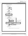
CHAPTER 2
CPU
2.1
2.2
2.3
2.4
2.5
2.6
2.7
CPU register
General-purpose registers
Control registers
Accumulator
Program counter
Data format
Notes on use of accumulator
CPU
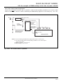
2.1 CPU register
2.1 CPU register
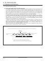
The M32R CPU has 16 general-purpose registers, 5 control registers, an accumulator and a program
counter. The accumulator is of 64-bit width. The registers and program counter are of 32-bit width.
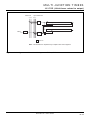
2.2 General-purpose registers
The 16 general-purpose registers (R0 to R15) are of 32-bit width and are used to retain data and base
addresses. R14 is used as the link register and R15 as the stack pointer (SPI or SPU). The link register
is used to store the return address when executing a subroutine call instruction. The interrupt stack pointer
(SPI) and the user stack pointer (SPU) are alternately represented by R15 depending on the value of the
stack mode bit (SM) in the processor status word register (PSW).
0
31
0
31
R0
R8
R1
R9
R2
R10
R3
R11
R4
R12
R5
R13
R6
R14 (link register)
R7
R15 (stack pointer) (see note)
Note: The interrupt stack pointer (SPI) and the user stack pointer (SPU) are alternatively
represented by R15 depending on the value of the stack mode bit (SM) in the PSW.
Fig. 2.2.1 General-purpose registers
2-2
M32150F4TFP User's Manual
CPU
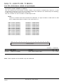
2.3 Control registers
2.3 Control registers
There are 5 control registers which are the processor status word register (PSW), the condition bit register
(CBR), the interrupt stack pointer (SPI), the user stack pointer (SPU) and the backup PC (BPC). The MVTC
and MVFC instructions are used for writing and reading these control registers.
(see notes)
CRn
CR0
0
31
PSW
processor status register
CR1
CBR
condition bit register
CR2
SPI
interrupt stack pointer
CR3
SPU
user stack pointer
CR6
BPC
backup PC
Notes 1: CRn (n = 0 to 3, 6) denotes the control register number.
2: The MVTC and MVFC instructions are used for writing and reading these control registers.
Fig. 2.3.1 Control registers
M32150F4TFP User's Manual
2-3
CPU
2.3 Control registers
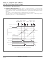
2.3.1 Processor status word register: PSW (CR0)
The processor status word register (PSW) shows the M32R CPU status. It consists of the current PSW
field, and the BPSW field where a copy of the PSW field is saved when EIT (For details, refer to Chapter 4
"EIT".) occurs.
The PSW field is made up of the stack mode bit (SM), the interrupt enable bit (IE) and the condition bit
(C).
The BPSW field is made up of the backup stack mode bit (BSM), the backup interrupt enable bit (BIE) and
the backup condition bit (BC).
BPSW field
0
PSW
7
8
15 16 17
23 24 25
0 0 0 0 0 0 0 0 0 0 0 0 0 0 0 0
BSM
PSW field
0 0 0 0 0
BIE
BC
31
0 0 0 0 0
SM
IE
C
D
Bit name
Function
init.
R
W
16
BSM (Backup SM)
Saves value of SM bit when EIT occurs
undefined
○
○
17
BIE (Backup IE)
Saves value of IE bit when EIT occurs
undefined
○
○
23
BC (Backup C)
Saves value of C bit when EIT occurs
undefined
○
○
24
SM (Stack mode)
0: Uses R15 as the interrupt stack pointer
0
○
○
0
○
○
0
○
○
1: Uses R15 as the user stack pointer
25
IE (Interrupt enable)
0: Does not accept interrupt
1: Accepts interrupt
31
C (Condition bit)
Indicates carry, borrow and overflow resulting
from operations (instruction dependent)
2-4
M32150F4TFP User's Manual
CPU
2.3 Control registers
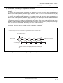
2.3.2 Condition bit register: CBR (CR1)
The condition bit register (CBR) is a separate register which contains the condition bit (C) in the PSW. The
value of the condition bit (C) in the PSW is reflected in this register. This register is read-only. An attempt
to write to the CBR with the MVTC instruction is ignored.
0
CBR
31
0 0 0 0 0 0 0 0 0 0 0 0 0 0 0 0 0 0 0 0 0 0 0 0 0 0 0 0 0 0 0 C
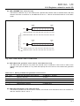
2.3.3 Interrupt stack pointer:
SPI (CR2)
User stack pointer:
SPU (CR3)
The interrupt stack pointer (SPI) and the user stack pointer (SPU) retain the current stack address. The
SPI and SPU can be accessed as the general-purpose register R15. R15 switches between representing
the SPI and SPU depending on the value of the stack mode bit (SM) in the PSW.
0
SPI
31
SPI
0
SPU
31
SPU
2.3.4 Backup PC: BPC (CR6)
The backup PC (BPC) is the register where a copy of the PC value is saved when EIT occurs. Bit 31 is
fixed at "0". When EIT occurs, the PC value immediately before EIT occurrence or that of the next
instruction is set (For details, refer to Chapter 4 "EIT".). The value of the BPC is reloaded to the PC when
the RTE instruction is executed. However, the values of the lower 2 bits of the PC become "00" on
returning (It always returns to the word boundary).
0
BPC
31
BPC
M32150F4TFP User's Manual
0
2-5
CPU
2.4 Accumulator
2.4 Accumulator
The accumulator (ACC) is a 64-bit register used for the DSP function.
Use the MVTACHI and MVTACLO instructions for writing to the accumulator. The high-order 32 bits (bit 0
to bit 31) can be set with the MVTACHI instruction and the low-order 32 bits (bit 32 to bit 63) can be set
with the MVTACLO instruction. Use the MVFACHI, MVFACLO and MVFACMI instructions for reading from
the accumulator. The high-order 32 bits (bit 0 to bit 31) are read with the MVFACHI instruction, the low order
32 bits (bit 32 to bit 63) with the MVFACLO instruction and the middle 32 bits (bit 16 to bit 47) with the
MVFACMI instruction.
The MUL instruction also uses the accumulator and the contents are destroyed when this instruction is
executed.
Read range with MVFACMI instruction
(see note)
0
78
15
16
31
32
47
48
63
ACC
Read/write range with
MVTACHI or MVFACHI instruction
Read/write range with
MVTACLO or MVFACLO instruction
Note: Bits 0 to 7 are always read as the sign-extended value of bit 8.
An attempt to write to this area is ignored.
2.5 Program counter
The program counter (PC) is a 32-bit counter that retains the address of the instruction being executed.
Since the M32R CPU instruction starts with even-numbered addresses, the LSB (bit 31) is always "0".
0
PC
2-6
31
PC
M32150F4TFP User's Manual
0
CPU
2.6 Data format
2.6 Data format
2.6.1 Data type
Signed and unsigned integers of byte (8 bits), halfword (16 bits), and word (32 bits) types are supported
as data in the M32R CPU instruction set. A signed integer is represented in a 2's complement format.
0
Signed byte (8-bit) integer
7
S
0
7
Unsigned byte (8-bit) integer
0
Signed halfword (16-bit) integer
15
S
0
15
Unsigned halfword (16-bit) integer
0
Signed word (32-bit) integer
31
S
0
31
Unsigned word (32-bit) integer
S: sign bit
Fig. 2.6.1 Data type
M32150F4TFP User's Manual
2-7
CPU
2.6 Data format
2.6.2 Data format
(1) Data format in a register
Data size of a register of the M32R CPU is always a word (32 bits).
Byte (8 bits) and halfword (16 bits) data in memory are sign-extended (the LDB and LDH instructions)
or zero-extended (the LDUB and LDUH instructions) to 32 bits, and loaded into the register.
Word (32 bits) data in a register is stored to memory by the ST instruction. Halfword (16 bits) data
in the LSB side of a register is stored to memory by the STH instruction. Byte (8 bits) data in the
LSB side of a register is stored to memory by the STB instruction.
< Load >
0
From memory
(LDB, LDUB instruction)
Sign-extention (LDB instruction) or
zero-extention (LDUB instruction)
31
24
Rn
Byte
Sign-extention (LDH instruction) or
zero-extention (LDUH instruction)
0
From memory (LDH, LDUH instruction)
31
16
Rn
Halfword
From memory (LD instruction)
0
Rn
31
Word
< Store >
0
24
Rn
31
Byte
To memory (STB instruction)
0
31
16
Halfword
Rn
To memory (STH instruction)
0
Rn
31
Word
To memory (ST instruction)
Fig. 2.6.2 Data format in a register
2-8
M32150F4TFP User's Manual
CPU
2.6 Data format
(2) Data format in memory
Data stored in memory can be one of these types: byte (8 bits), halfword (16 bits) or word (32 bits).
Although the byte data can be located at any address, the halfword data and the word data can only
be located on the halfword boundary and the word boundary, respectively. If an attempt is made to
access data in memory which is not located on the correct boundary, an address exception occurs.
Address
+ 0 number
0
+ 1 number
7 8
+ 2 number
15 16
+ 3 number
23 24
31
Byte
Byte
Byte
Byte
Byte
Halfword
Halfword
Halfword
Word
Word
Fig. 2.6.3 Data format in memory
M32150F4TFP User's Manual
2-9
CPU
2.7 Notes on use of accumulator
2.7 Notes on use of accumulator
After executing MVTACHI instruction, bits 8 to 15 of ACC become the unjust value by executing RAC or
RACH instruction.
So, at setting a value to ACC, it is necessary to execute MVTACLO instruction after executing MVTACHI
instruction.
This note restricts M32150F4TFP of M32R family.
2-10
M32150F4TFP User's Manual
CHAPTER 3
ADDRESS SPACE
3.1 Summary of address space
3.2 Operation modes
3.3 Internal ROM and expanded external area
3.4 Internal RAM and SFR area
3.5 EIT vector entry
3.6 ICU vector table
3.7 Notes on address space
ADDRESS SPACE
3.1 Summary of address space
3.1 Summary of address space
The M32150F4TFP provides a 4G-byte linear logical address space, and logical addresses are always
accessed by 32 bits wide. The address space of the M32150F4TFP contains the following areas:
(1) User area
• Internal ROM area
• Expanded external area
• Internal RAM area
• Special function registers (SFRs) area
(2) Reserved area (not open to users)
(3) System area (not open to users)
(1) User area
Two-Gbyte area of addresses H'0000 0000 to H'7FFF FFFF is the user area, where located are the
internal ROM, the expanded external area, the internal RAM and the special function registers area
(SFRs; the registers of the internal peripheral I/Os). However, the locations of the internal ROM and
the expanded external area vary depending on operation modes described later.
(2) Reserved area
One-Gbyte area of addresses H'8000 0000 to H'BFFF FFFF is reserved by MITSUBISHI for the
future development and is not open to users.
(3) System area
One-Gbyte area of addresses H'C000 0000 to H'FFFF FFFF is the system area, which is reserved
for such development support tools as in-circuit emulators or debugging monitors and is not open to
users.
3-2
M32150F4TFP User's Manual
ADDRESS SPACE
3.1 Summary of address space
Expanded external area
(1M bytes)
<M32150F4TFP logical space >
EIT vector entry
(see note)
Logical address
H'0000 0000
(16M bytes)
Internal ROM area
H'0000 0000
CS0 area
H'0007 FFFF
H'0008 0000
CS1 area
H'000F FFFF
Ghost areas of 1M-Bytes
quantities each
User area
Ghost areas of 16M-Bytes
quantities each
2G bytes
H'0010 0000
H'7FFF FFFF
H'8000 0000
1G bytes
H'007F FFFF
Reserved area
Internal RAM/SFR area
(16K byes)
H'0080 0000
H'0080 3FFF
H'0080 4000
H'BFFF FFFF
H'C000 0000
System area
Ghost areas of 16K-Bytes
quantities each
1G bytes
H'FFFF FFFF
H'00FF FFFF
Note: These locations vary depending on operation modes.
Fig. 3.1.1 Address space of M32150F4TFP
M32150F4TFP User's Manual
3-3
ADDRESS SPACE
3.2 Operation modes
3.2 Operation modes
The M32150F4TFP provides the following operation modes, which can be defined by the MOD0 and MOD1
pins. For the mode of reprogramming the internal flash memory, refer to Section 5.4 "Programming of
internal flash memory".
Table 3.2.1 Setting of operation modes
MOD0
MOD1 (see note 1)
Operation mode (see note 2)
VSS
VSS
Single chip mode
VSS
VCC
Expanded external mode
VCC
VSS
Processor mode
VCC
VCC
Reserved (Do not use)
Notes 1: VCC = +5 V, VSS = GND
2: Refer to Section 5.4 "Programming of internal flash memory" for the mode of reprogramming the
flash memory.
The locations of the internal ROM and the expanded external area vary depending on operation modes (the
other areas do not). The address maps of the internal ROM and the expanded external area in three modes
are shown in Figure 3.2.1. (For the mode of reprogramming the internal flash memory, refer to Section 5.4
"Programming of internal flash memory".)
Non CS0 area
(Internal ROM access area)
H'0000 0000
Internal ROM area
(128K bytes)
Internal ROM area
(128K bytes)
H'0007 FFFF
H'0008 0000
CS0 area
(384K bytes)
CS1 area
(512K bytes)
CS0 area
(512K bytes)
Expanded external area
Expanded external area
H'0001 FFFF
H'0002 0000
CS1 area
(512K bytes)
H'000F FFFF
<Single chip mode>
<Expanded external mode>
<Processor mode>
Fig. 3.2.1 Operation mode and internal ROM area/expanded external area
3-4
M32150F4TFP User's Manual
ADDRESS SPACE
3.3 Internal ROM and expanded external area
3.3 Internal ROM and expanded external area
The 8M-byte area of addresses H'0000 0000 to H'007F FFFF within the user area is assigned to the internal
ROM and the expanded external area, of which 1M bytes of addresses H'0000 0000 to H'000F FFFF are
user available, and the other addresses can be seen as ghosts of a 1M-byte quantity each (the ghost areas
should not be used inadvertently at programming).
For the relation between the locations of the internal ROM and expanded external area and the M32150F4TFP
operation modes, refer to Section 3.2 "Operation modes".
3.3.1 Internal ROM area
Addresses H'0000 0000 to H'0001 FFFF are assigned to the internal ROM (128K bytes), and at the starting
address, the EIT vector entry (and the ICU vector table) is located.
3.3.2 Expanded external area
The expanded external area begins at address H'0002 0000 if the expanded external mode is selected out
of the operation modes and at address H'0000 0000 if the processor mode selected. When external devices
access this area, the control signals they require are output.
Table 3.3.1 shows the addresses of the expanded external
area in ____
the three operation modes. When any
____
address within the CS0 or the CSI area is accessed, a CS0 or a CS1 signal is output respectively.
Table 3.3.1 Addresses of expanded external area in three operation modes
Operation mode
Addresses of expanded external area
Single chip mode
None
Expanded external mode
Addresses H'0002 0000 to H'0007 FFFF
(CS0 area : 384K bytes)
Addresses H'0008 0000 to H'000F FFFF
(CS1 area : 512K bytes)
Addresses H'0000 0000 to H'0007 FFFF
(CS0 area : 512K bytes)
Addresses H'0008 0000 to H'000F FFFF
(CS1 area : 512K bytes)
Processor mode
M32150F4TFP User's Manual
3-5
ADDRESS SPACE
3.4 Internal RAM and SFR area
3.4 Internal RAM and SFR area
The 8M-byte area of addresses H'0080 0000 to H'00FF FFFF is assigned to the internal RAM and the SFR
area, of which the 16K bytes of addresses H'0080 0000 to H'0080 3FFF are user available, and the other
addresses can be seen as ghosts of a 16K-byte quantity each (the ghost areas should not be used inadvertently
at programming).
3.4.1 Internal RAM area
Addresses H'0080 1000 to H'0080 27FF are assigned to the internal RAM (6K bytes).
3.4.2 SFR (Special Function Register) area
Addresses H'0080 0000 to H'0080 0FFF are assigned to the SFR area, where the registers of the internal
peripheral I/Os are located.
H'0080 0000
SFR area
(4K bytes)
H'0080 0FFF
H'0080 1000
Internal RAM
(6K bytes)
H'0080 27FF
H'0080 2800
H'0080 3FFF
Fig. 3.4.1 Internal RAM area/SFR (Special Function Register) area
3-6
M32150F4TFP User's Manual
ADDRESS SPACE
3.4 Internal RAM and SFR area
0
7 8
+0 number
15
+1 number
H'0080 0000
∼
0
7 8
+0 number
15
+1 number
H'0080 0400
Interrupt
controller
(ICU)
∼
H'0080 0468
DMAC
H'0080 007E
H'0080 0080
∼
A-D converter
H'0080 00AE
H'0080 0100
∼
H'0080 0700
Serial I/O
∼
H'0080 0118
I/O port
H'0080 074E
H'0080 0180
Wait controller
H'0080 07E0
H'0080 07E2
Flash control
H'0080 0200
∼
H'0080 023E
H'0080 0240
∼
MJT
(Units common)
MJT (TOP)
Multi-junction timers (MJTs)
H'0080 02FE
H'0080 0300
∼
MJT (TIO)
H'0080 03C0
∼
MJT (TMS)
H'0080 03E0
∼
H'0080 0FFF
TOP : 16-bit timers related to output
TIO : 16-bit timers related to input/output
TMS : 16-bit timers related to input
TML : 32-bit timers related to input
MJT (TML)
H'0080 03FE
Note: The real-time debugger (RTD) is an independent module operated by external devices
and not visible to the CPU.
Fig. 3.4.2 Address map of SFR area
M32150F4TFP User's Manual
3-7
ADDRESS SPACE
3.4 Internal RAM and SFR area
Address
+0 number
+1
number
D7 D8
D0
D15
Interrupt vector register (IVECT)
H'0080 0000
H'0080 0002
H'0080 0004
H'0080 0006
Interrupt mask register (IMASK)
SBI control register (SBICR)
∼
∼
∼
∼
H'0080 006C
A-D conversion interrupt control register (IADCCR)
SIO0 transmit interrupt control register (ISIO0TXCR)
H'0080 006E
SIO0 receive interrupt control register (ISIO0RXCR)
SIO1 transmit interrupt control register (ISIO1TXCR)
H'0080 0070
SIO1 receive interrupt control register (ISIO1RXCR)
H'0080 0072
MJT output interrupt control register 0 (IMJTOCR0)
MJT output interrupt control register 1 (IMJTOCR1)
H'0080 0074
MJT output interrupt control register 2 (IMJTOCR2)
MJT output interrupt control register 3 (IMJTOCR3)
H'0080 0076
MJT output interrupt control register 4 (IMJTOCR4)
MJT output interrupt control register 5 (IMJTOCR5)
H'0080 0078
MJT output interrupt control register 6 (IMJTOCR6)
MJT output interrupt control register 7 (IMJTOCR7)
H'0080 007A
MJT input interrupt control register 0 (IMJTICR0)
MJT input interrupt control register 1 (IMJTICR1)
H'0080 007C
MJT input interrupt control register 2 (IMJTICR2)
MJT input interrupt control register 3 (IMJTICR3)
H'0080 007E
MJT input interrupt control register 4 (IMJTICR4)
H'0080 0080
DMAC interrupt control register (IDMACCR)
Single mode register 0 (ADSIM0)
Single mode register 1 (ADSIM1)
Scan mode register 0 (ADSCM0)
Scan mode register 1 (ADSCM1)
H'0080 0082
H'0080 0084
H'0080 0086
H'0080 0088
A-D successive approximation register (ADSAR)
H'0080 008A
H'0080 008C
A-D comparate data register (ADCMP)
∼
∼
H'0080 0090
A-D data register 0 (ADDT0)
∼
∼
H'0080 0092
A-D data register 1 (ADDT1)
H'0080 0094
A-D data register 2 (ADDT2)
H'0080 0096
A-D data register 3 (ADDT3)
H'0080 0098
A-D data register 4 (ADDT4)
H'0080 009A
A-D data register 5 (ADDT5)
H'0080 009C
A-D data register 6 (ADDT6)
H'0080 009E
A-D data register 7 (ADDT7)
H'0080 00A0
A-D data register 8 (ADDT8)
H'0080 00A2
A-D data register 9 (ADDT9)
H'0080 00A4
A-D data register 10 (ADDT10)
H'0080 00A6
A-D data register 11 (ADDT11)
H'0080 00A8
A-D data register 12 (ADDT12)
H'0080 00AA
A-D data register 13 (ADDT13)
H'0080 00AC
A-D data register 14 (ADDT14)
H'0080 00AE
A-D data register 15 (ADDT15)
∼
∼
H'0080 0100
∼
∼
SIO0 mode register (S0MOD)
H'0080 0102
SIO0 control register 0 (S0CNT0)
H'0080 0104
SIO0 baud rate register (S0BAUR)
SIO0 transmit buffer register (S0TXB)
H'0080 0106
H'0080 0108
SIO0 control register 1 (S0CNT1 )
SIO0 interrupt mask register (S0MASK)
SIO0 status register (S0STAT)
SIO0 receive buffer register (S0RXB)
∼
∼
∼
∼
SIO1 mode register (S1MOD)
H'0080 0110
H'0080 0112
SIO1 control register 0 (S1CNT0)
SIO1 control register 1 (S1CNT1)
Fig. 3.4.3 Register mapping of SFR area (1)
3-8
M32150F4TFP User's Manual
ADDRESS SPACE
3.4 Internal RAM and SFR area
Address
+0 number
+1 number
D0
H'0080 0114
D7 D8
SIO1 baud rate register (S1BAUR)
∼
∼
H'0080 0180
SIO1 interrupt mask register (S1MAS)
SIO1 transmit buffer register (S1TXB)
H'0080 0116
H'0080 0118
D15
SIO1 receive buffer register (S1RXB)
SIO1 status register (S1STAT)
∼
∼
Wait number control register (WTCCR)
∼
∼
H'0080 0200
∼
∼
Clock bus & input event bus control register (CKIEBCR)
H'0080 0202
Prescaler register 0 (PRS0)
Prescaler register 1 (PRS1)
H'0080 0204
Prescaler register 2 (PRS2)
Output event bus control register (OEBCR)
∼
∼
H'0080 0210
∼
∼
TCLK input processor control register (TCLKCR)
H'0080 0212
TIN input processor control register 0 (TINCR0)
H'0080 0214
TIN input processor control register 1 (TINCR1)
H'0080 0216
H'0080 0218
TIN input processor register 2 (TINCR2)
TIN input processor control register 3 (TINCR3)
TIN input processor control register 4 (TINCR4)
H'0080 021A
H'0080 021C
H'0080 021E
F/F source select register 0 (FFS0)
H'0080 0220
F/F source select register 1 (FFS1)
H'0080 0222
H'0080 0224
F/F protect register 0 (FFP0)
H'0080 0226
F/F data register 0 (FFD0)
H'0080 0228
F/F protect register 1 (FFP1)
H'0080 022A
F/F data register 1 (FFD1)
H'0080 022C
H'0080 022E
H'0080 0230
TOP interrupt control register 0 (TOPIR0)
TOP interrupt control register 1 (TOPIR1)
H'0080 0232
TOP interrupt control register 2 (TOPIR)
TOP interrupt control register 3 (TOPIR3)
H'0080 0234
TIO interrupt control register 0 (TIOIR0)
TIO interrupt control register 1 (TIOIR1)
H'0080 0236
TIO interrupt control register 2 (TIOIR2)
TMS interrupt control register (TMSIR)
H'0080 0238
TIN interrupt control register 0 (TINIR0)
H'0080 023A
TIN interrupt control register 2 (TINIR2)
TIN interrupt control register 1 (TINIR1)
TIN interrupt control register 3 (TINIR3)
H'0080 023C
TIN interrupt control register 4 (TINIR4)
TIN interrupt control register 5 (TINIR5)
H'0080 023E
TIN interrupt control register 6 (TINIR6)
H'0080 0240
TOP0 counter (TOP0CT)
H'0080 0242
TOP0 reload register (TOP0RL)
H'0080 0244
TOP0 adjust register (TOP0CC)
H'0080 0246
∼
∼
H'0080 0250
∼
∼
TOP1 counter (TOP1CT)
TOP1 reload register (TOP1RL)
H'0080 0252
H'0080 0254
TOP1 adjust register (TOP1C)
H'0080 0256
∼
∼
∼
∼
H'0080 0260
TOP2 counter (TOP2CT)
H'0080 0262
TOP2 reload register (TOP2R)
H'0080 0264
TOP2 adjust register (TOP2CC)
H'0080 0266
Fig. 3.4.4 Register mapping of SFR area (2)
M32150F4TFP User's Manual
3-9
ADDRESS SPACE
3.4 Internal RAM and SFR area
Address
D0
+0 number
+1 number
D7 D8
D15
H'0080 0268
∼
∼
H'0080 0270
∼
∼
TOP3 counter (TOP3CT)
TOP3 reload register (TOP3R)
H'0080 0272
H'0080 0274
TOP3 adjust register (TOP3CC)
H'0080 0276
∼
∼
H'0080 0280
∼
∼
TOP4 counter (TOP4CT)
TOP4 reload register (TOP4RL)
H'0080 0282
H'0080 0284
TOP4 adjust register (TOP4CC)
H'0080 0286
∼
∼
H'0080 0290
∼
∼
TOP5 counter (TOP5CT)
TOP5 reload register (TOP5RL)
H'0080 0292
H'0080 0294
TOP5 adjust register (TOP5C)
H'0080 0296
H'0080 0298
H'0080 029A
TOP0 to TOP5 control register 0 (TOP05CR0)
TOP0 to TOP5 control register 1 (TOP05CR1)
H'0080 029C
H'0080 029E
H'0080 02A0
TOP6 counter (TOP6CT)
H'0080 02A2
TOP6 reload register (TOP6R)
H'0080 02A4
TOP6 adjust register (TOP6CC)
H'0080 02A6
H'0080 02A8
H'0080 02AA
TOP6, TOP7 control register (TOP67CR)
∼
∼
H'0080 02B0
∼
∼
TOP7 counter (TOP7CT)
TOP7 reload register (TOP7RL)
H'0080 02B2
H'0080 02B4
TOP7 adjust register (TOP7CC)
H'0080 02B6
∼
∼
H'0080 02C0
∼
∼
TOP8 counter (TOP8CT)
TOP8 reload register (TOP8RL)
H'0080 02C2
H'0080 02C4
TOP8 adjust register (TOP8CC)
H'0080 02C6
∼
∼
H'0080 02D0
∼
∼
TOP9 counter (TOP9C)
TOP9 reload register (TOP9RL)
H'0080 02D2
H'0080 02D4
TOP9 adjust register (TOP9CC)
H'0080 02D6
∼
∼
H'0080 02E0
∼
∼
TOP10 counter (TOP10CT)
TOP10 reload register (TOP10RL)
H'0080 02E2
H'0080 02E4
TOP10 adjust register (TOP10CC)
H'0080 02E6
H'0080 02E8
TOP8 to TOP10 control register (TOP810CR)
H'0080 02EA
Fig. 3.4.5 Register mapping of SFR area (3)
3-10
M32150F4TFP User's Manual
ADDRESS SPACE
3.4 Internal RAM and SFR area
Address
+0 number
+1 number
D7 D8
D0
D15
H'0080 02EC
∼
∼
H'0080 02FA
∼
∼
TOP0 to TOP10 external enable permit register (TOPEEN)
H'0080 02FC
TOP0 to TOP10 enable protect register (TOPPRO)
H'0080 02FE
TOP0 to TOP10 count enable register (TOPCEN)
H'0080 0300
TIO0 counter (TIO0CT)
H'0080 0302
H'0080 0304
TIO0 reload 1 register (TIO0RL1)
H'0080 0306
TIO0 reload 0/ measure register (TIO0RL0)
∼
∼
H'0080 0310
∼
∼
TIO1 counter (TIO1CT)
H'0080 0312
H'0080 0314
TIO1 reload 1 register (TIO1RL1)
H'0080 0316
TIO1 reload 0/ measure register (TIO1RL0)
H'0080 0318
H'0080 031A
TIO0 to TIO3 control register 0 (TIO03CR0)
TIO0 to TIO3 control register 1 (TIO03CR1)
H'0080 031C
H'0080 031E
H'0080 0320
TIO2 counter (TIO2CT)
H'0080 0322
H'0080 0324
TIO2 reload 1 register (TIO2RL1)
H'0080 0326
TIO2 reload 0/ measure register (TIO2RL0)
∼
∼
H'0080 0330
∼
∼
TIO3 counter (TIO3CT)
H'0080 0332
H'0080 0334
TIO3 reload 1 register (TIO3RL1)
H'0080 0336
TIO3 reload 0/ measure register (TIO3RL0)
∼
∼
H'0080 0340
∼
∼
TIO4 counter (TIO4CT)
H'0080 0342
H'0080 0344
TIO4 reload 1 register (TIO4RL1)
H'0080 0346
TIO4 reload 0/ measure register (TIO4RL0)
H'0080 0348
H'0080 034A
TIO4 control register (TIO4CR)
TIO5 control register (TIO5CR)
H'0080 034C
H'0080 034E
TIO5 counter (TIO5CT)
H'0080 0350
H'0080 0352
H'0080 0354
TIO5 reload 1 register (TIO5RL1)
H'0080 0356
TIO5 reload 0/ measure register (TIO5RL0)
∼
∼
H'0080 0360
∼
∼
TIO6 counter (TIO6CT)
H'0080 0362
H'0080 0364
TIO6 reload 1 register (TIO6RL1)
H'0080 0366
TIO6 reload 0/ measure register (TIO6RL0)
H'0080 0368
H'0080 036A
TIO6 control register (TIO6CR)
TIO7 control register (TIO7CR)
H'0080 036C
Fig. 3.4.6 Register mapping of SFR area (4)
M32150F4TFP User's Manual
3-11
ADDRESS SPACE
3.4 Internal RAM and SFR area
Address
D0
+0 number
+1 number
D7 D8
D15
H'0080 036E
H'0080 0370
TIO7 counter (TIO7CT)
H'0080 0372
H'0080 0374
TIO7 reload 1 register (TIO7RL1)
H'0080 0376
TIO7 reload 0/ measure register (TIO7RL0)
∼
∼
H'0080 0380
∼
∼
TIO8 counter (TIO8CT)
H'0080 0382
H'0080 0384
TIO8 reload 1 register (TIO8RL1)
H'0080 0386
TIO8 reload 0/ measure register (TIO8RL0)
H'0080 0388
H'0080 038A
TIO8 control register (TIO8CR)
TIO9 control register (TIO9CR)
H'0080 038C
H'0080 038E
TIO9 counter (TIO9CT)
H'0080 0390
H'0080 0392
H'0080 0394
TIO9 reload 1 register (TIO9RL1)
H'0080 0396
TIO9 reload 0/ measure register (TIO9RL0)
∼
∼
H'0080 03BC
H'0080 03BE
∼
∼
TIO0 to TIO9 enable protect register (TIOPRO)
TIO0 to TIO9 count enable register (TIOCEN)
H'0080 03C0
TMS0 counter (TMS0CT)
H'0080 03C2
TMS0 measure 3 register (TMS0MR3)
H'0080 03C4
TMS0 measure 2 register (TMS0MR2)
H'0080 03C6
TMS0 measure 1 register (TMS0MR1)
H'0080 03C8
H'0080 03CA
TMS0 measure 0 register (TMS0MR0)
TMS0 control register (TMS0CR)
TMS1 control register (TMS1CR)
H'0080 03CC
H'0080 03CE
TMS1 counter (TMS1CT)
H'0080 03D0
H'0080 03D2
TMS1 measure 3 register (TMS1MR3)
H'0080 03D4
TMS1 measure 2 register (TMS1MR2)
H'0080 03D6
TMS1 measure 1 register (TMS1MR1)
H'0080 03D8
TMS1 measure 0 register (TMS1MR0)
∼
∼
H'0080 03E0
TML counter high-order (TMLCTH)
∼
∼
TML counter low-order (TMLCTL)
H'0080 03E2
∼
∼
H'0080 03EA
∼
∼
TML control register (TMLCR)
H'0080 03EC
H'0080 03EE
H'0080 03F0
TML measure 3 register high-order (TMLMR3)
H'0080 03F2
TML measure 3 register low-order (TMLMR3L)
H'0080 03F4
TML measure 2 register high-order (TMLMR2H)
H'0080 03F6
TML measure 2 register low-order (TMLMR2L)
H'0080 03F8
TML measure 1 register high-order (TMLMR1H)
H'0080 03FA
TML measure 1 register low-order (TMLMR1L)
H'0080 03FC
TML measure 0 register high-order (TMLMR0H)
Fig. 3.4.7 Register mapping of SFR area (5)
3-12
M32150F4TFP User's Manual
ADDRESS SPACE
3.4 Internal RAM and SFR area
Address
+0 number
+1 number
D0
H'0080 03FE
D7 D8
D15
TML measure 0 register lower (TMLMR0L)
H'0080 03FF
H'0080 0400 DMA interrupt request status register (DMITST)
∼
∼
H'0080 0410
DMA0 channel control register (DM0CNT)
DMA interrupt mask register (DMITMK)
∼
∼
DMA0 transfer count register (DM0TCT)
H'0080 0412
H'0080 0414
H'0080 0416
DMA0 source address register (DM0SA)
H'0080 0418
H'0080 041A
DMA0 destination address register (DM0DA)
H'0080 041C
H'0080 041E
H'0080 0420
DMA1 channel control register (DM1CNT)
DMA1 transfer count register (DM1TCT)
H'0080 0422
H'0080 0424
H'0080 0426
DMA1 source address register (DM1SA)
H'0080 0428
H'0080 042A
DMA1 destination address register (DM1DA)
H'0080 042C
H'0080 042E
H'0080 0430
DMA2 channel control register (DM2CNT)
DMA2 transfer count register (DM2TCT)
H'0080 0432
H'0080 0434
H'0080 0436
DMA2 source address register (DM2SA)
H'0080 0438
H'0080 043A
DMA2 destination address register (DM2DA)
H'0080 043C
H'0080 043E
H'0080 0440
DMA3 channel control register (DM3CNT)
DMA3 transfer count register (DM3TCT)
H'0080 0442
H'0080 0444
H'0080 0446
DMA3 source address register (DM3SA)
H'0080 0448
H'0080 044A
DMA3 destination address register (DM3DA)
H'0080 044C
H'0080 044E
H'0080 0450
DMA4 channel control register (DM4CNT)
DMA4 transfer count register (DM4TCT)
H'0080 0452
H'0080 0454
H'0080 0456
DMA4 source address register (DM4SA)
H'0080 0458
H'0080 045A
DMA4 destination address register (DM4DA)
H'0080 045C
H'0080 045E
H'0080 0460
DMA0 software request generate register (DM0SRI)
H'0080 0462
DMA1 software request generate register (DM1SRI)
H'0080 0464
DMA2 software request generate register (DM2SRI)
H'0080 0466
DMA3 software request generate register (DM3SRI)
Fig. 3.4.8 Register mapping of SFR area (6)
M32150F4TFP User's Manual
3-13
ADDRESS SPACE
3.4 Internal RAM and SFR area
Address
+0 number
+1 number
D7 D8
D0
H'0080 0468
D15
DMA4 software request register (DM4SRI)
∼
∼
H'0080 0700
∼
∼
P0 data register (P0DATA)
P1 data register (P1DATA)
H'0080 0702
P2 data register (P2DATA)
P3 data register (P3DATA)
H'0080 0704
P4 data register (P4DATA)
H'0080 0706
P6 data register (P6DATA)
H'0080 0708
P8 data register (P8DATA)
P9 data register (P9DATA)
H'0080 070A
P10 data register (P10DATA)
P11 data register (P11DATA)
H'0080 070C
P12 data register (P12DATA)
P13 data register (P13DATA)
H'0080 070E
P14 data register (P14DATA)
P15 data register (P15DATA)
H'0080 0720
P0 direction register (P0DIR)
P1 direction register (P1DIR)
H'0080 0722
P2 direction register (P2DIR)
H'0080 0724
P4 direction register (P4DIR)
H'0080 0726
P6 direction register (P6DIR)
H'0080 0728
P8 direction register (P8DIR)
P9 direction register (P9DIR)
H'0080 072A
P10 direction register (P10DIR)
P11 direction register (P11DIR)
H'0080 072C
P12 direction register (P12DIR)
P13 direction register (P13DIR)
H'0080 072E
P14 direction register (P14DIR)
P15 direction register (P15DIR)
P6 operation mode register (P6MOD)
P7 operation mode register (P7MOD)
H'0080 0748
P8 operation mode register (P8MOD)
P9 operation mode register (P9MOD)
H'0080 074A
P10 operation mode register (P10MOD)
H'0080 074C
P12 operation mode register (P12MOD)
P13 operation mode register (P13MOD)
H'0080 074E
P14 operation mode register (P14MOD)
P15 operation mode register (P15MOD)
P7 data register (P7DATA)
∼
∼
∼
∼
H'0080 0746
∼
∼
P3 register (P3DIR)
P7 direction register (P7DIR)
∼
∼
P11 operation mode register (P11MOD)
∼
∼
∼
∼
H'0080 07E0
Flash mode register (FMOD)
H'0080 07E2
Flash control register (FCNT)
Block erase control register (FBLK)
∼
∼
H'0080 0FFE
∼
∼
Fig. 3.4.9 Register mapping of SFR area (7)
3-14
M32150F4TFP User's Manual
ADDRESS SPACE
3.5 EIT vector entry
3.5 EIT vector entry
The EIT vector entry is located at the top of the internal ROM and expanded external area, where the branch
instruction (not the branch address) to the starting address of each EIT handler is described. For detail refer
to Chapter 4 "EIT".
0
31
H'0000 0000
H'0000 0004
RI (Reset interrupt)
H'0000 0008
H'0000 000C
H'0000 0010
H'0000 0014
SBI (System break interrupt)
H'0000 0018
H'0000 001C
H'0000 0020
H'0000 0024
RIE (Reserved instruction exception)
H'0000 0028
H'0000 002C
H'0000 0030
H'0000 0034
AE (Address exception)
H'0000 0038
H'0000 003C
H'0000 0040
TRAP0
H'0000 0044
TRAP1
H'0000 0048
TRAP2
H'0000 004C
TRAP3
H'0000 0050
TRAP4
H'0000 0054
TRAP5
H'0000 0058
TRAP6
H'0000 005C
TRAP7
H'0000 0060
TRAP8
H'0000 0064
TRAP9
H'0000 0068
TRAP10
H'0000 006C
TRAP11
H'0000 0070
TRAP12
H'0000 0074
TRAP13
H'0000 0078
TRAP14
H'0000 007C
TRAP15
H'0000 0080
EI (External interrupt)
Fig. 3.5.1 EIT vector entry
M32150F4TFP User's Manual
3-15
ADDRESS SPACE
3.6 ICU vector table
3.6 ICU vector table
The ICU vector table is used by the on-chip interrupt controller. The starting address of the interrupt handler
corresponding to the interrupt request of each internal peripheral I/O is described on this table. Refer to
Chapter 13 "Interrupt controller" for detail.
0
31
H'0000 0094
MJT input interrupt 4 handler starting address
H'0000 0098
MJT input interrupt 3 handler starting address
H'0000 009C
MJT input interrupt 2 handler starting address
H'0000 00A0
MJT input interrupt 1 handler starting address
H'0000 00A4
MJT input interrupt 0 handler starting address
H'0000 00A8
MJT output interrupt 7 handler starting address
H'0000 00AC
MJT output interrupt 6 handler starting address
H'0000 00B0
MJT output interrupt 5 handler starting address
H'0000 00B4
MJT output interrupt 4 handler starting address
H'0000 00B8
MJT output interrupt 3 handler starting address
H'0000 00BC
MJT output interrupt 2 handler starting address
H'0000 00C0
MJT output interrupt 1 handler starting address
H'0000 00C4
MJT output interrupt 0 handler starting address
H'0000 00C8
DMAC interrupt handler starting address
H'0000 00CC
SIO1 receive interrupt handler starting address
H'0000 00D0
SIO1 transmit interrupt handler starting address
H'0000 00D4
SIO0 receive interrupt handler starting address
H'0000 00D8
SIO0 transmit interrupt handler starting address
H'0000 00DC
A-D converter interrupt handler starting address
Fig. 3.6.1 ICU vector table
3-16
M32150F4TFP User's Manual
ADDRESS SPACE
3.7 Notes on address space
3.7 Notes on address space
• Virtual flash emulation
The M32150F4TFP provides the function of mapping the top 4K bytes of the internal RAM to the bottom
4K bytes of the internal ROM (flash memory), called virtual flash emulation. For this function, refer to
Section 5.6 "Virtual flash emulation".
M32150F4TFP User's Manual
3-17
ADDRESS SPACE
3.7 Notes on address space
MEMORANDUM
3-18
M32150F4TFP User's Manual
CHAPTER 4
EIT
4.1 Summary of EIT
4.2 EIT events of M32150F4TFP
4.3 EIT processing procedure
4.4 EIT processing mechanism
4.5 EIT event acceptance
4.6 Save and return of PC and PSW
4.7 EIT vector entry
4.8 Exception processing
4.9 Interrupt processing
4.10 Trap processing
4.11 EIT priority
4.12 EIT processing example
EIT
4.1 Summary of EIT
4.1 Summary of EIT
While the CPU is executing a program, sometimes it is necessary to suspend executing, because a certain
event occurs, and execute another program. These kinds of events are referred to as EIT (Exception,
Interrupt, Trap).
(1) Exception
The event is related to the context being executed. It is generated by errors or violations that occur
during instruction execution. With the M32150F4TFP, the address exception (AE) and reserved
instruction exception (RIE) are of this type.
(2) Interrupt
The event is not related to the context being executed. It is generated by an external hardware
signal. With the M32150F4TFP, the external interrupt (EI), system break interrupt (SBI) and reset
interrupt (RI) are of this type.
(3) Trap
This is a software interrupt which is generated by executing the TRAP instruction. It is intentionally
added to the program by the programmer, as a system call.
EIT
Exception
Reserved Instruction Exception (RIE)
Address Exception (AE)
Interrupt
Reset Interrupt (RI)
System Brake Interrupt (SBI)
External Interrupt (EI)
Trap
Trap (TRAP)
Fig. 4.1.1 EIT events
4-2
M32150F4TFP User's Manual
EIT
4.2 EIT events of M32150F4TFP
4.2 EIT events of M32150F4TFP
4.2.1 Exception
(1) Reserved instruction exception (RIE)
The reserved instruction exception (RIE) occurs when execution of a reserved instruction (unimplemented
instruction) is detected.
(2) Address exception (AE)
The address exception (AE) occurs if an attempt is made to access an unaligned address with either
a load instruction or a store instruction.
4.2.2 Interrupt
(1) Reset interrupt (RI)
______
The reset interrupt (RI) is always accepted when the RESET signal is input. It has the highest
priority.
(2) System brake interrupt (SBI)
______
The system brake interrupt (SBI) is an emergency interrupt request from the SBI pin. It is used when
a break in power source or an error from an external watchdog timer is detected. After interrupt
processing, in principle, the SBI can use only the case that control does not return to the original
program that was executing when the interrupt executing.
(3) External interrupt (EI)
The external interrupt (EI) is an interrupt request from peripheral I/O controlled by interrupt controller.
The internal interrupt controller controls the interrupt priority by 7 levels.
4.2.3 Trap
The trap (TRAP) is a software interrupt which is generated by executing the TRAP instruction. A total
of 16 EIT vector entries are available for operands 0 to 15 of the TRAP instruction.
M32150F4TFP User's Manual
4-3
EIT
4.3 EIT processing procedure
4.3 EIT processing procedure
Part of EIT processing is automatically executed by hardware and part is executed by software (EIT handler)
programmed by the user. Except for the reset interrupt and the wakeup interrupt, processing procedures
when accepting the EIT event are as follows.
When the EIT is accepted, the M32150F4TFP carries out hardware pre-processing (write later) and then
branches to the EIT vector. A entry address allocated for each EIT in the EIT vector. This is where BRA
instruction ( instructions) to the EIT handlers are stored. (Note that these are not branch addresses.)
In hardware pre-processing of M32150F4TFP, the PC contents are saved in the backup PC (BPC) and the
PSW field of the PSW register are saved in the BPSW field of the same register.
The user should save the BPC and the PSW register (the BPSW field included), and general-purpose
registers to be used by the EIT handler in the stack. (Saving to the stack is the responsibility of the user
program.).
On the completion of execution of the EIT handler, the registers saved in the stack should be restored and
then the RTE instruction should be executed. Control of the EIT process changes to hardware post-processing,
which returns control to the original program (except occurrence of the SBI).
In hardware post-processing of M32150F4TFP, the BPC value is restored to the PC and the BPSW field of
the PSW register to the PSW field in the same register.
EIT request
generation
Instruction Instruction Instruction
A
B
C
Program restarts
Program suspended
EIT request accepted
Instruction Instruction ••••
C
D
Instruction
processing
cancel type
(RIE, AE)
PC fi BPC
PSW fi (B)PSW
Hardware
pre-processing
Instruction
processing
complete type
(EI, TRAP)
Hardware
post-processing
User programming process
EIT vector
entry
Branch
instruction
(SBI)
EIT handler except occurrence of the SBI
BPC, (B)PSW and
general-purpose
registers are saved
to stack
Handler
processing
SBI
(System brake
interrupt processing)
General-purpose
registers, (B)PSW
and BPC are
restored
RTE
instruction
Program completion or
system reset
Note: (B)PSW indicates the BPSW field of the PSW register.
Fig. 4.3.1 EIT processing procedure overview
4-4
M32150F4TFP User's Manual
(B)PSW fi PSW
BPC fi PC
EIT
4.4 EIT processing mechanism
4.4 EIT processing mechanism
The M32150F4TFP EIT processing is carried out in the M32R CPU and has a register for backupping of the
PC and the PSW (the BPC register and the BPSW field of the PSW register). The EIT processing mechanism
in the M32150F4TFP is shown Figure 4.4.1.
M32150F4TFP
AAAAAAAAA
AAAAAAAAA
AAAAAAAAA
AAAAAAAAA
AAAAAAAAA
AAAAAAAAA
AAAAAAAAA
AAAAAAAAA
AAAAAAAAA
AAAAAAAAA
AAAAAAAAA
AAAAAAAAA
AAAAAAAAA
AAAAAAAAA
AAAAAAAAA
AAAAAAAAA
M32R CPU
RI
RESET
RI
High
AE, RIE, TRAP
Priority
SBI
SBI
•
Internal •
•
peripheral •
••
I/O
Interrupt
controller
(ICU)
EI
SBI
EI
Low
IE flag
(PSW)
BPC
BPSW PSW
PC
PSW register
Fig. 4.4.1 EIT processing of M32150F4TFP
M32150F4TFP User's Manual
4-5
EIT
4.5 EIT event acceptance
4.5 EIT event acceptance
When an EIT event occurs, the M32150F4TFP suspends execution of the current program and branching
to the EIT handler occurs. The initiating event and accept timing for each EIT event is given below.
Table 4.5.1 EIT event acceptance
EIT event
Processing type
Accept timing
Value set in BPC
Reserved instruction
exception (RIE)
Instruction processing
cancel type
During instruction execution
PC value of the instruction where
RIE occurred
Address exception
(AE)
Instruction processing
cancel type
During instruction execution
PC value of the instruction where
AE occurred
Reset interrupt
(RI)
Iinstruction processing
abort type
Each machine
cycle
Undefined
System brake
interrupt (SBI)
Instruction processing
complete type
Each instruction
(word boundary)
PC value of the next instruction
External interrupt
(EI)
Instruction processing
complete type
Each instruction
(word boundary)
PC value of the next instruction
Trap
(TRAP)
Instruction processing
complete type
Each instruction
PC value of the TRAP
instruction + 4
4-6
M32150F4TFP User's Manual
EIT
4.6 Save and return of PC and PSW
4.6 Save and return of PC and PSW
Operation is as follows when the EIT event occurs and when the RTE instruction is executed.
(1) Hardware pre-processing when the EIT event occurs
➀ SM, IE and C bits saving
The SM, IE and C bits are saved in the PSW register.
BSM ‹
SM
BIE ‹
IE
BC ‹
C
➁ SM, IE and C bits updating
The SM, IE and C bits are updated in the PSW register.
SM ‹
not changed (RIE, AE, TRAP),
or cleared to "0" (SBI, EI, RI)
IE
‹
cleared to "0"
C
‹
cleared to "0"
➂ PC saving
The PC is saved.
BPC ‹
PC
Vector address setting
Vector address is set in the PC.
Processing switches to the EIT handler, after branching to the EIT vector and executing the branch
instruction (BRA instruction) stored there.
(2) Hardware post-processing when the RTE instruction is executed
1 BSM, BIE and BC bits restoring
The BSM, BIE and BC bits are returned from the PSW register.
SM ‹
BSM
IE
‹
BIE
C
‹
BC
2 BPC value restoring
The BPC value is returned from the BPC.
PC ‹
BPC
Note: After executing the RTE instruction, the values of the BSM, BIE and BC bits in the BPC and the PSW
register are undefined.
M32150F4TFP User's Manual
4-7
EIT
4.6 Save and return of PC and PSW
AA
AA
AAAA
AAAA
PSW
BPC
1
EIT accepted
3
2
1
AA
AA
‹
BC
3 PC saved
SM
BPC
‹
‹
PC
C
4 vector address is set to PC
PC
‹
vector address
0
BSM, BIE and BC bits restored
SM ‹ BSM
IE ‹ BIE
C
‹
IE
SM, IE and C bits updated
SM ‹ no change/0
‹ 0
IE
C
1
AAAA
AAAA
2
SM, IE and C bits saved
BSM ‹
BIE ‹
2
4
1
RTE instruction execution
PC
2 BPC value restored
PC
‹
BPC
BC
The value of BPC bit is undefined after
execution of the RTE instruction.
The value of BSM, BIE or BC bit
is undefined after execution of
the RTE instruction.
BPSW field
0
PSW
7
8
15 16 17
0 0 0 0 0 0 0 0 0 0 0 0 0 0 0 0
BSM
23 24 25
0 0 0 0 0
BIE
Fig. 4.6.1 Save and return of PC and PSW
4-8
PSW field
M32150F4TFP User's Manual
BC
31
0 0 0 0 0
SM
IE
C
EIT
4.7 EIT vector entry
4.7 EIT vector entry
EIT vector entries are located from address H'0000 0000 in the user space. The EIT vector entries are
shown below.
Table 4.7.1 EIT vector entry
name
notation
vector address
SM
IE
value set in BPC
Reset interrupt
RI
H'0000 0000
0
0
Undefined
0
PC value of the next instruction
(see note)
System brake
SBI
H'0000 0010
0
RIE
H'0000 0020
no change 0
interrupt
Reserved instruction
exception
Address exception
PC value of the instruction where
RIE occurred
AE
H'0000 0030
no change 0
PC value of the instruction where
AE occurred
Trap
External interrupt
TRAP0
H'0000 0040
no change 0
PC value of the TRAP instruction + 4
TRAP1
H'0000 0044
no change 0
PC value of the TRAP instruction + 4
TRAP2
H'0000 0048
no change 0
PC value of the TRAP instruction + 4
TRAP3
H'0000 004C
no change 0
PC value of the TRAP instruction + 4
TRAP4
H'0000 0050
no change 0
PC value of the TRAP instruction + 4
TRAP5
H'0000 0054
no change 0
PC value of the TRAP instruction + 4
TRAP6
H'0000 0058
no change 0
PC value of the TRAP instruction + 4
TRAP7
H'0000 005C
no change 0
PC value of the TRAP instruction + 4
TRAP8
H'0000 0060
no change 0
PC value of the TRAP instruction + 4
TRAP9
H'0000 0064
no change 0
PC value of the TRAP instruction + 4
TRAP10
H'0000 0068
no change 0
PC value of the TRAP instruction + 4
TRAP11
H'0000 006C
no change 0
PC value of the TRAP instruction + 4
TRAP12
H'0000 0070
no change 0
PC value of the TRAP instruction + 4
TRAP13
H'0000 0074
no change 0
PC value of the TRAP instruction + 4
TRAP14
H'0000 0078
no change 0
PC value of the TRAP instruction + 4
TRAP15
H'0000 007C
no change 0
PC value of the TRAP instruction + 4
EI
H'0000 0080
0
PC value of the next instruction
0
Note : At the flash memory reprogramming, the vector address of reset interrupt moves to the starting
address of internal RAM (address H'0080 1000). Refer to section 5.4 "Programming of internal flash
memory".
M32150F4TFP User's Manual
4-9
EIT
4.8 Exception processing
4.8 Exception processing
4.8.1 Reserved instruction exception (RIE)
[Occurrence condition]
The RIE occurs when attempted execution of a reserved instruction (unimplemented instruction) is
detected. An instruction check is made on the instruction op code.
When RIE occurs, that instruction is not executed. Also note that, the RIE is accepted even if an
external interrupt has been requested.
[EIT processing]
(1) SM, IE and C bits saving
The SM, IE and C bits in the PSW register are saved.
BSM ‹
SM
BIE
‹
IE
BC
‹
C
(2) SM, IE and C bits updating
The SM, IE and C bits in the PSW register are updated.
SM
‹
not changed
IE
‹
0
C
‹
0
(3) PC saving
The PC value of the instruction that caused the RIE is set in the BPC. For example, if the
instruction caused the RIE is in address 4, "4" is set in the BPC. If it is address 6, then "6" is set.
In this case, the value of bit 30 in the BPC indicates whether the instruction that caused the RIE
is on the word boundary (BPC[30] = 0) or not (BPC[30] = 1).
In both of the above cases, however, the return address of the RTE instruction, after the EIT
handler processing, becomes address 4 because the lowest 2 bits are cleared to "00" when
returning the BPC value to the PC.
(4) Branching to the EIT vector entry
Processing branches to address H'0000 0020 in user space. The M32150F4TFP carries out hardware
pre-processing up to this point.
(5) Branching from the EIT vector entry to the EIT handler
The M32150F4TFP executes the BRA instruction written in address H'0000 0020 of the EIT vector
entry, and branches to the top address of the handler. At the top address of the EIT handler, the
BPC, the PSW register and any necessary general-purpose registers should be saved in the stack.
(6) Returning from the EIT handler
At the end of execution of the EIT handler, the general-purpose registers, the BPC and the PSW
register should be returned from the stack and the RTE instruction executed. When the RTE
instruction is executed, hardware post-processing is carried out automatically.
4-10
M32150F4TFP User's Manual
EIT
4.8 Exception processing
+0
+1
+2
+3
+0
Address
Return
address
H'00
H'04
H'08
H'0C
+1
+2
+3
Address
RIE occurrence
BPC
Return
address
H'00
H'04
H'08
H'0C
H'04
RIE occurrence
BPC
H'06
Fig. 4.8.1 Reserved instruction exception (RIE) return address example
M32150F4TFP User's Manual
4-11
EIT
4.8 Exception processing
4.8.2 Address Exception (AE)
[Occurrence condition]
The AE occurs if an attempt is made to access an unaligned address with either a load instruction
or store instruction. Instructions and address combinations which cause the address exception are
as follows:
• when executing the LDH, LDUH and STH instructions and the lowest 2 bits of the address are
"01" or "11".
• when executing the LD, ST, LOCK and UNLOCK instructions and the lowest 2 bits of the
address are "01", "10" or "11".
When AE occurs, memory access by the initiating instruction is not carried out and the AE is
accepted even if an external interrupt has been requested.
[EIT processing]
(1) SM, IE and C bits saving
The SM, IE and C bits in the
BSM ‹
BIE ‹
BC ‹
PSW register are saved.
SM
IE
C
(2) SM, IE and C bits updating
The SM, IE and C bits in the PSW register are updated.
SM ‹ not changed
IE
‹ 0
C
‹ 0
(3) PC saving
The PC value of the instruction that caused the AE is set in the BPC. For example, if the instruction
which caused the AE is in address 4, "4" is set in the BPC. If it is address 6, then "6" is set. In
this case, the value of bit 30 in the BPC indicates whether the instruction that caused the AE is
on the word boundary (BPC[30] = 0) or not (BPC[30] = 1).
In both of the above cases, however, the return address of the RTE instruction after EIT handler
processing becomes address 4 because the lowest 2 bits are cleared to "00" when returning the
BPC value to the PC.
(4) Branching to the EIT vector entry
Processing branches to address H'0000 0030 in user space. The M32150F4TFP carries out hardware
pre-processing up to this point.
(5) Branching from the EIT vector entry to the EIT handler
The M32150F4TFP executes the BRA instruction written in address H'0000 0030 of the EIT vector
entry, and branches to the top address of the handler. At the beginning of the EIT handler, the
BPC, the PSW register and any necessary general-purpose registers should be saved in the stack.
(6) Returning from the EIT handler
At the end of the EIT handler, the general-purpose registers, the BPC and the PSW register should
be returned from the stack and the RTE instruction executed. When the RTE instruction is executed,
hardware post-processing is carried out automatically.
4-12
M32150F4TFP User's Manual
EIT
4.8 Exception processing
+0
+1
+2
+0
+3
Return
address
+2
+3
Address
Address
H'00
H'04
H'08
H'0C
+1
AE occurrence
BPC
Return
address
H'04
H'00
H'04
H'08
H'0C
AE occurrence
BPC
H'06
Fig. 4.8.2 Address exception (AE) return address example
M32150F4TFP User's Manual
4-13
EIT
4.9 Interrupt processing
4.9 Interrupt processing
4.9.1 Reset interrupt (RI)
[Occurrence condition]
______
When an "L" level is input to the RESET pin, the reset interrupt is always accepted for any machine
cycle. The reset interrupt has the highest priority of all EIT events.
[EIT processing]
(1) SM, IE and C bits initialization
The SM, IE and C bits in the PSW register are initialized.
SM
‹
0
IE
‹
0
C
‹
0
When a reset interrupt is generated, the values of the BSM, BIE and BC bits are undefined.
(2) Branching to the EIT vector entry
Processing branches to address H'0000 0000 in user space. At the flash memory rewriting
(VPP = +12 V), the vector address of reset interrupt moves the starting address of internal RAM
(address H'0080 1000). Refer to section 5.4 "Programming of internal flash memory".
(3) Branching from the EIT vector entry to the user program
The M32150F4TFP executes the instruction written in address H'0000 0000 (reset vector entry) of
the EIT vector entry, and branches to the top address of the reset handler. In the reset handler,
the PSW register and the SPI should be initialized, and then branch to the top address of the user
program.
4-14
M32150F4TFP User's Manual
EIT
4.9 Interrupt processing
4.9.2 System break interrupt (SBI)
______
The SBI is an interrupt request from the SBI pin. It is used when a break in power source or an error from
an external watchdog timer is detected. It is not masked by the IE bit in the PSW register.
It is used in the case that some problem has already occurred until the system when the interrupt is
detected, such as a break in power source or an error from an external watchdog timer. In this case, use
of the SBI is under the condition that after SBI handler processing, control does not return to the original
program that was executing when the SBI occurred.
[Occurrence condition]
______
The SBI accepts when a fall edge is input to the SBI pin (The SBI is not masked by the IE bit in the
PSW register.).
The SBI does not start immediately after a 16-bit instruction on the word boundary is executed
(However, with a 16-bit branch instruction, the SBI is accepted immediately after branching.).
Instruction execution sequence
Address 1000
1002
1004
16-bit instruction 16-bit instruction
Interrupt
accept
O.K.
Interrupt
accept
No
1008
32-bit instruction
Interrupt
accept
O.K.
Interrupt
accept
O.K.
Fig. 4.9.1 System brake interrupt (SBI) accept timing
M32150F4TFP User's Manual
4-15
EIT
4.9 Interrupt processing
[EIT processing]
(1) SM, IE and C bits saving
The SM, IE and C bits in the PSW register are saved.
BSM ‹
SM
BIE ‹
IE
BC ‹
C
(2) SM, IE and C bits updating
The SM, IE and C bits in the PSW register are updated.
SM ‹
0
IE
‹
0
C
‹
0
(3) PC saving
The contents of the PC (always a word boundary value) are saved to the BPC.
(4) Branching to the EIT vector entry
Processing branches to address H’0000 0010 in user space. The M32150F4TFP carries out hardware
pre-processing up to this point.
(5) Branching from the EIT vector entry to the EIT handler
The M32150F4TFP executes the BRA instruction written in address H'0000 0010 of the EIT vector
entry, and branches to the top address of the EIT handler.
The SBI is used in the case that some problem has already occurred until the system when the
interrupt is detected. Use of the SBI is under the condition that after SBI handler processing,
control does not return to the original program that was executing when the SBI occurred.
4-16
M32150F4TFP User's Manual
EIT
4.9 Interrupt processing
4.9.3 External interrupt (EI)
The EI is an interrupt request from an internal interrupt controller. In the internal interrupt controller the
interrupt controls by 7 levels priority. About detail of interrupt controller, refer to chapter 13 "Interrupt
controller", about detaile of interrupt sources, refer to each chapter of internal peripheral I/O.
[Occurrence condition]
The EI is controlled by the internal interrupt controller based on the interrupt request from each of
the internal peripheral I/Os. The M32R CPU checks the request at the instruction break point on the
word boundary. If there is an interrupt and if the IE bit in the PSW register is "1", the EI is accepted.
The EI does not start immediately after the 16-bit instruction on the word boundary is executed
(However, with a 16-bit branch instruction, the EI is accepted immediately after branching.).
Instruction execution sequence
Address 1000
1002
1004
16-bit instruction 16-bit instruction
Interrupt
accept
O.K.
Interrupt
accept
No
1008
32-bit instruction
Interrupt
accept
O.K.
Interrupt
accept
O.K.
Fig. 4.9.2 External interrupt (EI) accept timing
M32150F4TFP User's Manual
4-17
EIT
4.9 Interrupt processing
[EIT processing]
(1) SM, IE and C bits saving
The SM, IE and C bits in the PSW register are saved.
BSM ‹
SM
BIE ‹
IE
BC ‹
C
(2) SM, IE and C bits updating
The SM, IE and C bits in the PSW register are updated.
SM ‹
0
IE
‹
0
C
‹
0
(3) PC saving
The contents of the PC (always a word boundary value) is saved to the BPC.
(4) Branching to the EIT vector entry
Processing branches to address H’0000 0080 in user space. The M32150F4TFP carries out hardware
pre-processing up to this point.
(5) Branching from the EIT vector entry to the EIT handler
The M32150F4TFP executes the BRA instruction written in address H'0000 0080 of the EIT vector
entry, and branches to the top address of the EIT handler. At the top address of the EIT handler,
the BPC, the PSW register and any necessary general-purpose registers should be saved in the
stack.
(6) Returning from the EIT handler
At the end of the external interrupt EIT handler, return the general-purpose registers, the BPC and
the PSW register from the stack and execute the RTE instruction.
When the RTE instruction is executed, hardware post-processing is automatically carried out.
4-18
M32150F4TFP User's Manual
EIT
4.10 Trap processing
4.10 Trap processing
4.10.1 Trap (TRAP)
[Occurrence condition]
The trap is a software interrupt which is generated by executing the TRAP instruction. A total of 16
traps are available and specified by operands 0 to 15 of the TRAP instruction 16 matching EIT vector
entries are available.
[EIT processing]
(1) SM, IE and C bits saving
The SM, IE and C bits in the PSW register are saved.
BSM ‹
SM
BIE ‹
IE
BC ‹ C
(2) SM, IE and C bits updating
The SM, IE and C bits in the PSW register are updated.
SM ‹
not changed
IE
‹
0
C
‹
0
(3) PC saving
When a TRAP instruction is executed, "PC value in the TRAP instruction + 4" is set in the BPC.
For example, if the TRAP instruction is in address 4, "8" is set in the BPC. If it is address 6, then
"10" is set. In this case, the value of bit 30 in the BPC indicates whether the TRAP instruction that
caused the trap is within the word boundary (BPC[30] = 0) or not (BPC[30] = 1).
In both of the above cases, however, the return address of the RTE instruction after EIT handler
processing is completed becomes address 8 because the lowest 2 bits are cleared to "00" when
returning the BPC value to the PC.
When a program is created with a standard Mitsubishi assembler, the assembler automatically
inserts an NOP instruction to the halfword immediately following a TRAP instruction located on the
word boundary.
(4) Branching to the EIT vector entry
Processing branches to one of addresses H’0000 0040 to H'0000 007C in user space depending
on the TRAP instruction operand value. The M32150F4TFP carries out hardware pre-processing
up to this point.
(5) Branching from the EIT vector entry to the EIT handler
The M32150F4TFP executes the BRA instruction written at the relevant address H’0000 0040 H'0000 007C of the EIT vector entries, and branches to the top address in the EIT handler. At the
top address of the EIT handler, the BPC, the PSW register and any necessary general-purpose
registers should be saved in the stack.
(6) Returning from the EIT handler
At the end of the EIT handler, the general-purpose registers, the BPC and the PSW register should
be returned from the stack and the RTE instruction executed. When the RTE instruction is executed,
hardware post-processing is carried out automatically.
M32150F4TFP User's Manual
4-19
EIT
4.10 Trap processing
+0
+1
+2
+3
+0
Address
Return
address
H'00
H'04
H'08
H'0C
+2
+3
Address
TRAP instruction
Return
address
BPC
H'08
Fig. 4.10.1 Trap (TRAP) return address example
4-20
+1
M32150F4TFP User's Manual
H'00
H'04
H'08
H'0C
TRAP instruction
BPC
H'08
EIT
4.11 EIT priority
4.11 EIT priority
The EIT event priority is as follows. When multiple EIT events occur simultaneously, the higher priority event
is accepted first.
Table 4.11.1 EIT event priority
Priority
EIT event
Processing type
1 (highest)
Reset interrupt (RI)
Instruction abort type
2
Address exception (AE)
Instruction cancel type
Reserved instruction exception (RIE)
Instruction cancel type
Trap (TRAP)
Instruction complete type
3
System brake interrupt (SBI)
Instruction complete type
4
External interrupt (EI)
Instruction complete type
The priority of each interrupt request from peripheral I/Os in the EI is set by internal interrupt controller.For
detail, refer to Chapter 13 "Interrupt controller".
M32150F4TFP User's Manual
4-21
EIT
4.12 EIT processing example
4.12 EIT processing example
(1) RIE, AE, SBI, EI and TRAP single-occurrence
IE = 1
BPC = return address A
IE = 0
RIE, AE, SBI, EI or TRAP
single-occurrence
EITs other than reset and SBI
cannot be accepted if IE = 0
return address A:
IE = 1
RTE instruction
: EIT handler
Fig. 4.12.1 Processing of RIE, AE, SBI, EI or TRAP event
(2) RIE, AE, TRAP or EI occurred simultaneously
RIE, AE and TRAP is accepted first
BPC = return address A
IE = 1
IE = 0
RTE instruction
RIE, AE, TRAP or EI occurred
simultaneously
return address A:
IE = 1
IE = 0
IE = 1
EI is accepted after higher priority processing
is completed BPC = return address A
RTE instruction
: EIT handler
Fig. 4.12.2 Processing of RIE, AE, EI or TRAP simultaneous occurrence
4-22
M32150F4TFP User's Manual
EIT
4.12 EIT processing example
EIT vector entry
BRA instruction
(Except occurrence of the SBI)
(SBI)
EIT handler
Hardware
pre-processing
PC fi BPC
PSW fi BPSW
BPC stack saving
(see note)
PSW stack saving
General-purpose
registers saving
Program
EIT event
occurrence
•
•
•
•
•
•
SBI
System brake
interrupt processing
Program completion
system reset
EIT handler processing
•
•
•
•
•
•
General-purpose
registers restoration
Hardware
post-processing
BPSW fi PSW
BPC fi PC
(see note)
PSW register restoration
BPC restoration
RTE
Fig. 4.12.3 EIT processing example
M32150F4TFP User's Manual
4-23
EIT
4.12 EIT processing example
MEMORANDUM
4-24
M32150F4TFP User's Manual
CHAPTER 5
INTERNAL MEMORY
5.1 Summary of internal memory
5.2 Internal RAM
5.3 Internal flash memory
5.4 Programming of internal flash memory
5.5 Registers related to internal flash memory
5.6 Virtual flash emulation
INTERNAL MEMORY
5.1 Summary of internal memory
5.1 Summary of internal memory
The M32150F4TFP is provided with the following memories.
• 6K-byte RAM
• 128K-byte flash memory
5.2 Internal RAM
The specification of the internal RAM of M32150F4TFP is shown in Table 5.2.1.
Table 5.2.1 Specification of internal RAM
Item
Specification
Size
6K bytes
Addresses
H'0080 1000 to H'0080 27FF
Wait insertion
No wait operation (at 25 MHz internal operation)
Internal bus connection
32-bit bus
Dual port
Data can be read (monitored) from and written to the whole area of
internal RAM externally with serial communications of RTD (real-time
debugger) independently of CPU.
5.3 Internal flash memory
The specification of the internal flash memory of the M32150F4TFP is shown in Table 5.3.1.
Table 5.3.1 Specification of internal flash memory
Item
Specification
Size
128K bytes
Addresses
H'0000 0000 to H'0001 FFFF
Wait insertion
No wait operation (at 25 MHz internal operation)
Internal bus connection
32-bit bus
Other
Virtual flash emulation (refer to Section 5.6 "Virtual flash emulation")
5-2
M32150F4TFP User's Manual
INTERNAL MEMORY
5.4 Registers related to internal flash memory
5.4 Registers related to internal flash memory
The register map related to the internal flash memory is shown in Figure 5.4.1.
Address
+0 number
D0
+1 number
D7 D8
H'0080 07E0
Flash mode register
(FMOD)
H'0080 07E2
Flash control register
(FCNT)
D15
Block erase control register
(FBLK)
Fig. 5.4.1 Register map related to internal flash memory
M32150F4TFP User's Manual
5-3
INTERNAL MEMORY
5.4 Registers related to internal flash memory
5.4.1 Flash mode register (FMOD)
<Address : H'0080 07E0>
D0
1
2
3
4
5
6
D7
FMOD
<at reset : H'00>
D
Bit name
0 to 6
Not assigned.
7
FMOD (Flash mode)
Function
0: VPPL (+ 5V) applied to VPP
Ini.
R
W
0
0
-
0
○
-
(ordinary mode)
1: VPPH (+12 V) applied to VPP
Note: This register is read-only.
The flash mode register (FMOD) is read-only and is read a 1 when VPPH (+12 V) is applied to the VPP
pin.
5-4
M32150F4TFP User's Manual
INTERNAL MEMORY
5.4 Registers related to internal flash memory
5.4.2 Flash control register (FCNT)
<Address : H'0080 07E2>
D0
1
2
3
4
5
6
FENTRY
D7
FEMMOD
<at reset : H'00>
D
Bit name
0 to 2
Not assigned.
3
FENTRY (Flash mode entry)
Function
0: Ordinary mode
Ini.
R
W
0
0
-
0
○
○
0
0
-
0
○
○
1: Flash mode if +12 V applied to VPP
and this bit set to 1
4 to 6
Not assigned.
7
FEMMOD
0: Ordinary mode
(Virtual flash emulation mode)
1: Virtual flash emulation mode;
the top 4 KB of RAM is mapped at
the bottom 4 KB of flash memory.
The flash control register (FCNT) contains the following two bits for controlling the flash memory.
(1) FENTRY (Flash mode entry bit D3)
The flash memory enters the flash mode only if VPPH (+12 V) is applied to the VPP pin and this bit
is set to 1.
(2) FEMMOD (Virtual flash emulation mode bit D7)
The flash memory enters the virtual flash emulation mode if this bit is set to 1. In the virtual flash
emulation mode, the top 4K bytes of the internal RAM (H'0080 1000 to H'0080 1FFF) is mapped at
the bottom 4K bytes of the internal flash memory (H'0001 F000 to H'0001 FFFF). (Refer to Section
5.6 "Virtual flash emulation")
M32150F4TFP User's Manual
5-5
INTERNAL MEMORY
5.4 Registers related to internal flash memory
5.4.3 Block erase control register (FBLK)
<Address : H'0080 07E3>
D8
9
10
11
12
13
14
D15
FERSBLK
<at reset : H'00>
D
Bit name
8 to 13
Not assigned.
14, 15
FERSBLK (Block erase)
Function
00: Whole area selected
Ini.
R
W
0
0
-
0
○
○
01: Block 0 selected
10: Block 1 selected
11: Whole area selected (the same as in 00) (see note)
Note: Writing by means of selecting blocks makes the feature for writing farther than normal writing
significant, as a result, the data-holding characteristics improve.
This feature, if used under the condition of writing infrequently during mass production, brings
out merits.
In instances in which writing frequently occurs as in developing or making a prototype, use
this feature under the condition of selecting the whole areas rather than selecting blocks to
increase the frequency of use.
The block erase control register (FBLK) can select the whole area of the 128K-byte flash memory or either
of the two 64K-byte blocks of it to be erased. These blocks are as follows:
Block 0: H'0000 0000 to H'0000 FFFF
Block 1: H'0001 0000 to H'0001 FFFF
This register must be set before issuing the program or the erase command. The block not selected cannot
be programmed or erased because the voltage required is not applied to the block.
5-6
M32150F4TFP User's Manual
INTERNAL MEMORY
5.5 Programming of internal flash memory
5.5 Programming of internal flash memory
5.5.1 Outline of programming flash memory
How to program the flash memory of the M32150F4TFP is explained in the following two cases.
(1) The software for programming is not loaded in the flash memory.
(2) The software for programming has been loaded in the flash memory.
In the case of (1), first the software for programming the flash memory is transferred to the internal RAM
using the dedicated serial I/O, RSIF (RAM Serial InterFace). The RSIF becomes available by applying
+12 V (VPPH) to the MOD1 pin after the VPP pin (power supply to the flash memory) is pulled to VPPH.
This state is called the RSIF mode, for the period of which the M32150F4TFP is held reset.
After the software for programming is transferred to the RAM in the RSIF mode, VPPH is removed from
the MOD1 pin to allow the M32150F4TFP exiting the reset state. Then, the FENTRY bit of the flash control
register (FCNT) is set to 1, and the M32150F4TFP enters the flash mode. In this mode, the reset vector
entry moves into the starting address of the internal RAM (usually it is at the starting address of the flash
memory). Thus, the software for programming transferred to the RAM begins to program the flash memory.
In the case of (2), any event generated (for instance, an input to the selected pin) causes the software for
programming loaded in the flash memory to be transferred to the RAM, and control jumps to the starting
address of the transferred program. At this time, applying VPPH (+12 V) to the MOD1 pin (the voltage
applied can be detected by the FMOD bit of the flash mode register) followed by setting the FENTRY bit
of the flash control register to 1 causes the M32150F4TFP to enter the flash mode. Thus, the software for
programming transferred to the RAM begins to program the flash memory.
M32150F4TFP User's Manual
5-7
INTERNAL MEMORY
5.5 Programming of internal flash memory
+5 V
VCC or VSS
VPPL
AAAAA
AAA
AA
AAAAA
AAAAAAAAAA
AAA
AA
AAAAA
AAAAAAAAAA
VPP
MOD1
RAM
< Step 1>
•Initial state (software for programming not loaded in flash memory)
CPU
FLASH
RSIF
Software for
programming
SIO0
Data for
programming
memory
RSIF : RAM Serial InterFace
External device
M32150F4TFP
+12 V
VPPH
< Step 2>
• Apply VPPH (+12 V) to MOD1 after VPP pulled to VPPH (+ 12 V)
• M32150F4TFP held reset
• Serial transfer mode to internal RAM in the RISF mode
• Transfer of software for programming in the RISF mode
AA
AA
AAA
AA
AAA
AAA
AA
AAAAA
AAAAAAAAAA
VPP
RAM
MOD1
Software for
programming
CPU
FLASH
memory
RSIF
Software for
programming
SIO0
Data for
programming
M32150F4TFP
+12 V
External device
VCC or VSS
VPPH
AA
AAA
AAA
AA
AAAAA
AAAAAAA
AAAAAAA
VPP
RAM
< Step 3>
• VPPH (+12 V) removed from MOD1
• M32150F4TFP released from reset
• Reset vector moves into starting address of internal RAM
• FENTRY bit of flash control register set to 1
• Software for programming transferred to internal RAM begins writing
to flash memory
• Ordinary mode restored by lowering VPP to VPPL (+5 V) after writing
Flash
memory
MOD1
Software for
programming
CPU
Data for
RSIF
Software for
programming
SIO0
Data for
programming
programming
M32150F4TFP
External device
Fig. 5.5.1 Programming procedure to internal flash memory (Software for programming not loaded
in flash memory)
5-8
M32150F4TFP User's Manual
INTERNAL MEMORY
5.5 Programming of internal flash memory
+5 V
VCC or VSS
VPPL
AA
AAA
AAA
AA
AAAAA
AA
AAA
AAAAA
AAAAA
AAAAAAA
VPP
FLASH
memory
MOD1
RAM
CPU
Software for
programing
RSIF
< Step 1>
• Initial State (software for programming loaded in flash memory)
• M32150F4TFP executing usual program in flash memory
Data for
programming
SIO0
M32150F4TFP
+5 V
RSIF : RAM Serial InterFace
External device
VCC or VSS
VPPL
< Step 2>
• Any event (e.g., input to selected pin) signals flash memory to be
programmed (example)
• Software for programming in flash memory transferred to internal RAM
• Control jumps to starting address of internal RAM after transfer
AA
AA
AAA
AA
AAA
AA
AAA
AA
AAAAA
AAAAAAAAAA
VPP
RAM
Flash
memory
MOD1
Software for
programing
CPU
Software for
programing
RSIF
Data for
programming
SIO0
M32150F4TFP
+12 V
External device
VCC or VSS
VPPH
AAAAA
AAA
AA
AAAAA
AA
AA
VPP
RAM
Software for
programing
Flash
memory
Data for
programing
MOD1
CPU
RSIF
SIO0
M32150F4TFP
< Step 3>
• Apply VPPH (+12 V) to VPP
• Reset vector moves into starting address of RAM
(resetting not needed; if reset, program starts at starting address of
internal RAM)
• FENTRY bit of flash control register set to 1
• Software for programming transferred to internal RAM begins writing
to flash memory
• Ordinary mode restored by lowering VPP to VPPL (+5 V) after writing
Data for
programing
External device
Fig. 5.5.2 Programming procedure to internal flash memory (Software for programming loaded in
flash memory)
M32150F4TFP User's Manual
5-9
INTERNAL MEMORY
5.5 Programming of internal flash memory
5.5.2 Operation modes at programming flash memory
The operation modes at programming the flash memory is defined by the MOD0, MOD1 and VPP pins.
Table 5.5.1 shows the pin settings and the operation modes at programming the flash memory.
Table 5.5.1 Pin settings and operation modes at programming flash memory
MOD0
MOD1
VPP
FENTRY
Operation mode
Reset vector
(see note 1)
VSS
VSS
VSS
VSS
VCC
VPPH
VPPL
-
Single chip mode
Starting address of flash memory
VPPH
0
Single chip mode
Starting address of RAM
1
Flash mode
Starting address of RAM
VPPL
-
Expanded external mode
Starting address of flash memory
VPPH
0
Expanded external mode
Starting address of RAM
1
Flash mode
Starting address of RAM
-
RSIF mode
Starting address of RAM
VPPH
Notes 1: FENTRY bit of flash control register (FCNT) (-: Don't care)
2: VCC = +5 V, VSS = GND, VPPL = +5 V, VPPH = +12 V
(1) Flash mode
The flash mode is used to program and erase the internal flash memory of the M32150F4TFP. In this
mode, the program in the flash memory cannot be executed (data can be read by issuing the read
command described in Section 5.5.4). If necessary, therefore, the program in the flash memory
should be transferred to the internal RAM to be subject to its program prior to entering the flash
mode.
(2) Entering flash mode
The M32150F4TFP can enter the flash mode only from the single chip or the expanded external
mode by applying VPPH (+12 V) to the VPP pin and setting the FENTRY bit of the flash control
register (FCNT) to 1. It cannot enter this mode from the processor mode (MOD0 = VCC, MOD1 =
VSS).
(3) VPP voltage and reset vector
When VPPH (+12 V) is applied to the VPP pin, the reset vector entry always moves into the starting
address of the internal RAM. If, at this time, the FENTRY bit of the flash control register is set to 1,
the M32150F4TFP enters the flash mode (unless the RSIF mode is selected).
(4) RSIF mode
In the RSIF mode, the dedicated serial I/O, RSIF (RAM Serial InterFace), for writing to the RAM is
validated. The M32150F4TFP enters reset in this mode.
(5) Entering RSIF mode
To enter the RSIF mode, VPPH (+12 V) is applied to the MOD1 pin after the same voltage is applied
to the VPP pin.
To transfer the software for programming the flash memory through the RSIF from the external
device to the internal RAM, voltage VPPH (+12 V) is applied to the VPP and MOD1 pins, and then
only the MOD1 pin is lowered after the software has been transferred, so that the programming starts
at the starting address of the RAM where the reset vector entry has moved.
5-10
M32150F4TFP User's Manual
INTERNAL MEMORY
5.5 Programming of internal flash memory
5.5.3 RSIF (RAM Serial InterFace)
(1) Outline of RSIF
The RSIF (RAM Serial InterFace) is the dedicated serial I/O for transferring software for programing
from an external device to the internal RAM when the software for programming the flash memory
is not loaded in it (for instance, the flash memory is blank just after shipment). The RSIF is used only
to transfer data from the external device to the internal RAM and does not operate in the ordinary
operation modes. This interface is not provided with any registers that can be controlled by the CPU,
and its input and output pins serve those of channel 0 (SIO0) of the internal serial I/O alternately.
To use the RSIF, VPPH (+12 V) is applied to the MOD1 pin after the same voltage is applied to the
VPP pin to invoke the RSIF mode. In this mode the M32150F4TFP enters the reset state.
The RSIF is provided with the function of only writing data to the internal RAM, not with that of
reading data from the RAM. Furthermore, the RSIF can write binary data only, and the data it
transfers is stored at the fixed starting address of the RAM. (Addresses where data is stored cannot
be designated by the external device. )
Table 5.5.2 Description of RSIF
Item
Description
Type and number
UART with 1 channel
of channels
Transfer mode
Reception only (LOW level is output from RTX when error occurs)
Data format
Start bit = 1 bit (fixed)
Character length = 8 bits (fixed)
Parity bit = even (fixed)
Stop bit = 1 bit (fixed)
Order of transfer = LSB first fixed
Baud rate
f(BCLK) = at 25 MHz : 48828 bits/s
f(BCLK) = at 20 MHz : 39063 bits/s
Error detection
Parity and flaming errors (if error occurs, reception disabled, and RTX goes LOW)
Area available
Internal RAM area of 4 KB (H'0080 1000 to H'0080 1FFF); starting address fixed
for transfer
(Variable )
Baud rate generator
for SIO0
Serial I/O
channel 0 (SIO0)
RXD
P83 / RXD0 / RRX
TXD
P82 / TXD0 / RTX
(Fixed 1/512)
BCLK
Baud rate generator
for RSIF
RSIF
(RAM Serial InterFace)
RXD
TXD
RSIF mode control
Fig. 5.5.3 Configuration of RSIF (RAM Serial InterFace)
M32150F4TFP User's Manual
5-11
INTERNAL MEMORY
5.5 Programming of internal flash memory
(2) Error detection by RSIF
The RSIF can detect two errors as shown in Table 5.5.3.
Table 5.5.3 Error detection by RISF
Error
Description
Framing error
Occurs when stop bit of received data is not 1 bit
Parity error
Occurs when parity of received data is not even
If any error is detected and the RTX pin goes "L".
To return from the error, remove VPPH (+12 V) from the MOD1 pin and apply it to the pin to initialize
the RSIF. Then, restart data transfer.
5-12
M32150F4TFP User's Manual
INTERNAL MEMORY
5.5 Programming of internal flash memory
5.5.4 Procedure of programming internal flash memory
The flash memory can be programmed with the software for programming loaded in the internal RAM after
the flash mode is selected. In the flash mode, the internal flash memory cannot be read as in the other
operation modes. As a result, any program on the flash memory cannot be executed, so the software for
programming the flash memory should be loaded in the internal RAM prior to entering the flash mode. (In
the flash mode, byte- and word-accesses to the flash memory are inhibited.)
The flash memory can be accessed by issuing commands to addresses of the memory. These commands
are shown in Table 5.5.4.
Table 5.5.4 Commands used in flash mode
Name
Issued command data
Read command
H'0000
Program command
H'4040
Program verify command
H'C0C0
Erase command
H'2020
Erase verify command
H'A0A0
Each address on the memory which has been loaded with any command becomes accessible. However,
the address loaded with the read command after verifying the memory has no significance; the address to
which the verify command was written prior to issuing the read command has been latched and is valid
as the read address.
Note that the block erase control register (FBLK) must be set before issuing the program or the erase
command (refer to Section 5.4.4). The erase command can erase the whole area of the 128K-byte flash
memory or either of the two 64K-byte blocks of it. These blocks are as follows.
Block 0: H'0000 0000 to H'0000 FFFF
Block 1: H'0001 0000 to H'0001 FFFF
When either 64K-byte block is selected, the other cannot be programmed or erased.
(1) Read command
Read command H'0000 is loaded in the address to be read from the internal flash memory (the read
mode), and the contents at this address can be read out.
(2) Program command
To program the flash memory, first, dummy data is read at the address to be written. Then, program
command H'4040 is loaded in this address. A dummy read must be performed to have a constant
depth of writing (to preventing from excessive writing and erasure).
The block erase control register (FBLK) must be set before issuing the program command (refer to
Section 5.4.4 "Block erase control register (FBLK)"). Either one block or the whole area selected can
be programmed.
Programming is carries out automatically by the internal control circuit, it waits for 10 ms using the
software or the hardware timer by completing of program.
(3) Program verify command
It is necessary to verify the result of programming. To verify the written program, verify command
H'C0C0 is loaded in the address at which program begins, and then the program is read. The
program should be verified with the verify command, not the read command.
M32150F4TFP User's Manual
5-13
INTERNAL MEMORY
5.5 Programming of internal flash memory
(4) Erase command
The erase command is used to erase the contents of the internal flash memory. To erase the
memory, erase command H'2020 is loaded twice in an arbitrary address of the memory to preventing
a fault in erasure.
The block erase control register (FBLK) must be set before issuing the erase command (refer to
Section 5.4.4 "Block erase control register (FBLK)"). Either one block or the whole area selected can
be erased.
Note that, however, an arbitrary address is allowed to be loaded with this command independently
of the setting of the block erase control register.
Programming is carries out automatically by the internal control circuit, it waits for 9.5 ms using the
software or the hardware timer by completing of program.
(5) Erase verify command
It is necessary to verify the result of erasing. To verify the written program, erase verify command
H'A0A0 is loaded in the address at which erase begins, and then the program is read.
The erase shoud be verified with the erase verify command.
If commands are issued continuously, it is necessary to adjust their timings. Flow charts of command
execution are shown in Figures 5.5.4 to 5.5.6.
At erasing, the program command loads "0" to all area before erasing by arranging the memory
thresold value of erasing.
Reading of flash
Load read command H'0000
in address to be read
2 or more clock wait
Read contents at address to be read
End
Fig. 5.5.4 Sequences of reading flash memory
5-14
M32150F4TFP User's Manual
For timing adjustment
INTERNAL MEMORY
5.5 Programming of internal flash memory
Erasing of flash
For writing H'0000 to the all area
of flash memory
Program command
Load erase command H'2020
in an arbitrary address of internal flash area
2 or more clock wait
For timing adjustment
Load erase command H'2020
in an arbitrary address of internal flash area
2 or more clock wait
For timing adjustment
Wait for 9.5 ms
(using hardware or software timer)
Load erase verify command (H'A0A0) in
address to verify
Wait for 6 ms
(using hardware or software timer)
Read address to verify
NO
Verify OK ?
NO
YES
Retry 2000 times
YES
NO
Is it last address?
YES
NG
End erase command H'0000
Load
in an arbitrary address of internal flash area
Set next address
For initializing of flash control circuit
End
Fig. 5.5.5 Sequences of erasing flash memory
M32150F4TFP User's Manual
5-15
INTERNAL MEMORY
5.5 Programming of internal flash memory
Writing of flash
Load read command H'0000
in address to be written
Dummy read
(Essential execution)
For timing adjustment
2 or more clock wait
Read contents at address to be written
Load program command H'4040
in address at which program to begin
For timing adjustment
2 or more clock wait
Load program in address at which program
to begin
2 or more clock wait
For timing adjustment
Wait for 10 ms
(using software or hardware timer )
Load verify command H'C0C0 in address
at which program to begin
Wait for 6 ms
(using software or hardware timer )
Read address at which program to begin
NO
NO
Retry 25 times
YES
Is program OK?
YES
NO
Is it last address?
YES
Load read command H'0000
in address to be written
NG
End
Fig. 5.5.6 Sequences of programming flash memory
5-16
M32150F4TFP User's Manual
Set next address
For initializing of flash control circuit
INTERNAL MEMORY
5.5 Programming of internal flash memory
5.5.5 Time required to program flash memory
The time required to program the flash memory are shown below.
(1) Transfer time by RSIF (at transfer data size of 1K bytes)
1/39063 bps × 1 frame × 11 transfer bits × 1K bytes ≒ 0.3 s
(2) Transfer time by SIO (at transfer data size of 128K bytes)
1/39063 bps × 1 frame ×11 transfer bits × 128K bytes ≒ 36.0 s
(3) Flash memory programming time
16 ms (programming + verification) × 2 (average number of retries*) × 64K bytes (data size) ≒ 2.0 s
(4) Erase time (for whole area of 128K bytes)
(Writing "0" to all area) + (erase)≒6.0[s]
(5) Total time required to program flash memory (for whole area of 128K bytes)
At flash memory blank
: (1) + (2) + (3) = 38.3 s
At flash memory re-programmed : (2) + (3) + (4) = 44.0 s
*: The average number of retries is only a reference value. Also, the CPU time for calculation
is excluded because it is of a negligible order.
M32150F4TFP User's Manual
5-17
INTERNAL MEMORY
5.5 Programming of internal flash memory
5.5.6 External protection circuit of VPP/MOD1 pins
By applying the high voltage in the VPP/MOD1 pins, it is necessary to add the external protection circuit
to the pin without applying the pin to the voltage beyond maximum ratings. (Especially VPP pin is important
for VPP voltage stabilization at loading and erasing to flash. )
Figure 5.5.7 is shown the example of condenser's arrangement for removing the high and low frequency
noise.
M32150F4TFP
VPP
1.0 mF
0.01 mF
MOD1
0.01 mF
Fig. 5.5.7 Example of condenser's arrangement for VPP power souce
5-18
M32150F4TFP User's Manual
INTERNAL MEMORY
5.6 Virtual flash emulation
5.6 Virtual flash emulation
The M32150F4TFP provides the function of mapping the top 4K bytes of the internal RAM (H'0080 1000 to
H'0080 1FFF) to the bottom 4K bytes of the internal flash memory (H'0001 F000 to H'0001 FFFF), which
is called virtual flash emulation. This function together with the on-chip real-time debugger (RTD) facilitate
such data tuning that the data table on the internal flash memory can be referenced or rewritten externally.
However, the flash memory should be written after the virtual flash emulation mode is terminated.
5.6.1 Area available for virtual flash emulation
Figure 5.6.1 shows the area where virtual flash emulation function is available. However, it is within user's
discretion how to use this area.
<Internal flash>
In virtual flash emulation mode,
access to this area is replaced
by access to internal RAM
H'0000 0000
<Internal RAM>
H'0080 1000
H'0001 F000
4K bytes
4K bytes
H'0080 1FFF
H'0001 FFFF
H'0080 27FF
In virtual flash emulation mode,
this area is accessible as ordinary
internal RAM
Fig. 5.6.1 Virtual flash emulation area
5.6.2 Entering virtual flash emulation mode
To enter the virtual flash emulation mode, a 1 is written to the FEMMOD bit of the flash control register
(FCNT). When this bit is set to 1, the bottom 4K bytes of the flash memory are replaced by the top 4K bytes
of the internal RAM.
M32150F4TFP User's Manual
5-19
INTERNAL MEMORY
5.6 Virtual flash emulation
MEMORANDUM
5-20
M32150F4TFP User's Manual
CHAPTER 6
RESET
6.1 Summary of reset
6.2 Reset operation
6.3 Internal states immediately after
leaving reset
RESET
6.1 Summary of reset
6.1 Summary of reset
______
______
The M32150F4TFP enters the reset state when the RESET pin is strapped "L". Then, pulling the RESET
pin "H" removes reset, and the program counter indicates the address of the reset vector entry at which
program is executed.
6.2 Reset operation
6.2.1 Reset at power on
At power
on, until the oscillation of the on-chip multiply-by-two clock generator of M32150F4TFP is stabilized,
______
the RESET pin must be tied "L".
6.2.2 Reset during operation
______
To reset the M32150F4TFP during its operation, the RESET pin must be tied "L" for more than 4 clocks
of the XIN signal.
6.2.3 Reset vector at rewriting flash memory
When a voltage of +12 V is applied to the VPP pin, the reset vector entry moves to the starting address
of the internal RAM (address H'0080 1000). For detail, refer Section 5.4 "Programming of internal flash
memory".
6.3 Internal states immediately after leaving reset
The internal states of the M32150F4TFP immediately after leaving reset are shown in Table 6.3.1. For the
initial states of the registers associated with the internal peripheral I/Os, refer to the chapter of each of them.
Table 6.3.1 Internal states immediately after leaving reset
Register
PSW
State after reset
(CR0)
B'0000 0000 0000 0000 ??00 000? 0000 0000
(BSM, BIE, BC bit = Undefined)
CBR
(CR1)
H'0000 0000
SPI
(CR2)
Undefined
SPU
(CR3)
Undefned
BPC
(CR6)
Undefined
PC
ACC
H'0000 0000
(Accumulator)
(C bit = 0)
(executes at address H'0000 0000)
(see note)
Undefined
Note: At rewriting the flash memory (+12 V is applied to VPP), the PC indicates the starting address of the
RAM (H'0080 1000).
6-2
M32150F4TFP User's Manual
CHAPTER 7
EXTERNAL BUS
INTERFACE
7.1 Signals related to external bus interface
7.2 Read/write operations
7.3 Bus arbitration
EXTERNAL BUS INTERFACE
7.1 Signals related to external bus interface
7.1 Signals related to external bus interface
The M32150F4TFP provides the signals related to the external bus interface described below. These signals
are used in the expanded external mode or the processor mode.
(1) Address bus (A13 to A30)
The M32150F4TFP outputs an 18-bit address bus signal (A13 to A30) capable of addressing 512K
bytes of memory
space.____
The least significant bit A31 is not output. In the external write cycle, byte
____
write outputs BHW and BLW directly indicate that to which byte of the 16-bit data bus valid data is
written. In the read cycle, data is always read as 16 bits wide, and the data in the valid byte position
is transferred.
____
____
(2) Chip selects (CS0, CS1)
___
____
In the expanded external mode, CS0 or CS1 is output whenever a memory reference is made to the
upper or lower half 512K bytes of the 1-Mbyte expanded external area, respectively. However,
when
____
a memory reference is made to the area that is assigned to the internal flash memory, CS0 cannot
be output (refer to Chapter 3 "Address space").
___
(3) Read
strobe (RD)
___
___
RD is output during an external read cycle, indicating the read timing of read data. RD goes HIGH
at a write.
____
(4) Byte
high write (BHW)
____
BHW ____
indicates that the valid data is transferred on the upper byte (DB0 to DB7) of the 16-bit data
bus. BHW goes HIGH in the external read cycles.
____
(5) Byte
low write (BLW)
____
BLW ____
indicates that the valid data is transferred on the lower byte (DB8 to DB15) of the 16-bit data
bus. BHW goes HIGH in the external read cycles.
(6) Data bus (DB0 to DB15)
The 16-bit data bus is used to access external devices.
(7) System clock (BCLK)
BCLK outputs the clock of 25 MHz at 25 MHz internal operation and is used to design synchronous
external systems.
_____
(8) Wait (WAIT)
When invoking the _____
external bus cycles, the M32150F4TFP inserts wait cycles automatically for the
period of time the WAIT signal is active. For detail, refer to Chapter 14 "Wait controller".
The M32150F4TFP always inserts one or more wait cycles at the access to its external device, so
that the minimum access to the external device takes one wait cycles (2 BCLK cycles).
7-2
M32150F4TFP User's Manual
EXTERNAL BUS INTERFACE
7.1 Signals related to external bus interface
_____
_____
(9) Hold controls (HREQ, HACK)
The HOLD state is the state at which the M32150F4TFP stops bus accesses, and the pins related
to the bus interface are held high-impedance states. While the M32150F4TFP is at this state, the
external bus master
can transfer data using the system bus.
_____
Strapping the HREQ pin LOW causes the M32150F4TFP to enter the HOLD
state. During the HOLD
_____
state after the reception of a hold _____
request or the transition to this state, HACK goes LOW. To return
to the normal state from HOLD, HREQ is tied HIGH.
The state of each pin during HOLD is shown in Table 7.1.1.
Table 7.1.1 States of Pins during HOLD
Pin names
State or operation of pin
____
____
___
____
____
A13 to A30, DB0 to DB15, CS0, CS1, RD, BHW, BLW
High-impedance
_____
HACK
LOW output
Other pins
Normal state
(10) P7 operation mode register (P7MOD)
<Address : H'0080 0747>
The WAIT pin and P71, the HREQ pin and P72, and the HACK pin and P73 share a single pin. Port
P7 operation mode register selects the function of port P7. The construction of port P7 mode operation
mode register is shown as follows.
P7 operation mode register (P7MOD)
D8
9
10
11
P70MOD P71MOD P72MOD P73MOD
<Address : H'0080 0747>
12
13
14
D15
P74MOD P75MOD P76MOD P77MOD
<at reset : H'00>
D
8
Bit name
P70MOD
(Port P70 operation mode)
9
P71MOD
Function
R
W
0: P70
?
○
?
○
?
○
?
○
?
○
?
○
?
○
?
○
1: BCLK
0: P71
_____
(Port P71 operation mode)
10
P72MOD
1: WAIT
0: P72
_____
(Port P72 operation mode)
11
P73MOD
1: HREQ
0: P73
_____
(Port P73 operation mode)
12
P74MOD
(Port P74 operation mode)
13
P75MOD
(Port P75 operation modd)
14
P76MOD
(Port P76 operation mode)
15
P77MOD
(Port P77 operation mode)
1: HACK
0: P74
1: RTDTXD
0: P75
1: RTDRXD
0: P76
1: RTDACK
0: P77
1: RTDCLK
R = ? : Undefined readout value
M32150F4TFP User's Manual
7-3
EXTERNAL BUS INTERFACE
7.2 Read/write operations
7.2 Read/write operations
____
____
___
External
read/write
operations are performed with the address
bus, the data bus, ____
and the CS0,
CS1, RD,
____
____
_____
___
____
BHW, BLW, and WAIT signals. In the external read cycle, RD goes LOW, and both BHW and BLW go HIGH
to read data at the required byte position.
____
____
In the external write cycle, either BHW or BLW goes LOW according to the byte position to be written.
_____
In external bus cycles, waits are inserted successively if WAIT is held LOW, so it should be tied HIGH if
not needed. The M32150F4TFP always inserts no less than one cycles at the access to its external device,
so that the minimum access to the external device takes one wait (2 BCLK cycles).
Bus vacant
Internal bus access
BCLK
A13 to A30
CS0. CS1
RD
"H"
BHW, BLW
"H"
Hi-Z
DB0 to DB15
WAIT
Note : Hi-Z represents a high-impedance state.
Fig. 7.2.1 Internal bus access at bus vacant
7-4
M32150F4TFP User's Manual
EXTERNAL BUS INTERFACE
7.2 Read/write operations
Read
Read
(2 cycles)
1 wait
BCLK
A13 to A30
CS0. CS1
RD
BHW, BLW
"H"
A
DB0 to DB15
WAIT
A
"H"
Write
(2 cycles)
Write
1 wait
BCLK
A13 to A30
CS0. CS1
RD
"H"
BHW, BLW
DB0 to DB15
WAIT
A
"H"
Note: "○"s represent sampling timings in the above illustration.
Fig. 7.2.2 Read/write timings (at minimum external access)
M32150F4TFP User's Manual
7-5
EXTERNAL BUS INTERFACE
7.2 Read/write operations
Read
Read (4 cycles)
External
1 wait
Internal 2 waits
BCLK
A13 to A30
CS0. CS1
RD
BHW, BLW
"H"
DB0 to DB15
WAIT
AA
AA
AA
AAAA
"H"
(Don't care)
Write
"L"
Write (4 cycles)
External
1 wait
Internal 2 waits
BCLK
A13 to A30
CS0. CS1
RD
"H"
BHW, BLW
DB0 to DB15
WAIT
AA AA
AAAA
"H"
(Don't care)
"L"
Note: "○"s represent sampling timings in the above illustration.
Fig. 7.2.3 Read/write timings (at 2-internal + 1-external wait access)
7-6
M32150F4TFP User's Manual
EXTERNAL BUS INTERFACE
7.3 Bus arbitration
7.3 Bus arbitration
______
When
a LOW input to the HREQ pin is accepted, the M32150F4TFP enters the HOLD state to drive the
_____
HACK pin LOW. During HOLD, the pins associated with the bus interface are held high-impedance
states,
_____
and data can be transferred on the system bus. To return to the normal state from HOLD, HREQ is tied
HIGH.
Bus cycle
Idle
Enters
HOLD
Hold state
Return
Next bus cycle
BCLK
HREQ
HACK
A13 to A30
CS0, CS1
Hi-Z
RD
Hi-Z
BHW, BLW
Hi-Z
DB0 to DB15
Hi-Z
WAIT
Notes 1: "○" represents a sampling timing in the above illustration.
2: Hi-Z represents a high impedance state.
Fig. 7.3.1 Bus arbitration timing
M32150F4TFP User's Manual
7-7
EXTERNAL BUS INTERFACE
7.3 Bus arbitration
MEMORANDUM
7-8
M32150F4TFP User's Manual
CHAPTER 8
I/O PORT AND
PIN FUNCTION
8.1
8.2
8.3
8.4
Summary of I/O ports
Selection of pin functions
Registers related to I/O ports
Port peripheral circuit
I/O PORT AND PIN FUNCTION
8.1 Summary of I/O ports
8.1 Summary of I/O ports
The M32150F4TFP is provided with I/O ports P0 to P15 (P5 is MITSUBISHI reserved), which consist of a
total of 109 I/O pins. These pins can be designated as input or output pins with their port direction registers.
Each port pin serves the alternative function of an internal peripheral I/O port pin/an expanded external
busline, and the function of each port pin can be defined by the MOD0 and MOD1 pins or the corresponding
I/O port operation mode register (port pins that serve two peripheral I/O pin functions should further be
specified by the corresponding register of each peripheral I/O).
The outline of the I/O port pins is shown in Table 8.1.1.
Table 8.1.1 Outline of I/O port pins
Item
Description
Number of pins
109 in total
Port function
P0:
P00 to P07
(8)
P1:
P10 to P17
(8)
P2:
P20 to P27
(8)
P3:
P30 to P37
(8)
P4:
P41 to P47
(7)
P6:
P61 to P67
(7)
P7:
P70 to P77
(8)
P8:
P82 to P87
(6)
P9:
P93 to P97
(5)
P10: P100 to P107
(8)
P11: P110 to P117
(8)
P12: P124 to P127
(4)
P13: P130 to P137
(8)
P14: P140 to P147
(8)
P15: P150 to P157
(8)
Each port pin can be selected as input or output by setting corresponding bit
of port direction register (P64 is SBI input-only port)
Pin function
Alternative function of peripheral I/O pin/expanded external busline
(or triple functions of peripheral I/O pins)
Selection of pin function
P0 to P4 Pins
: Using operation mode definition pins MOD0 and MOD1
P6 to P15 Pins
: Using operation mode register of each port
(peripheral I/O pin functions are selectable by corresponding
register of peripheral I/O)
8-2
M32150F4TFP User's Manual
I/O PORT AND PIN FUNCTION
8.2 Selection of pin function
8.2 Selection of pin function
Each port pin serves the alternative function of an internal peripheral I/O port pin/an expanded external
busline (or triple functions of peripheral I/O pins), and the function of each port pin can be defined by the
MOD0 and MOD1 pins or the corresponding I/O port operation mode register.
When the expanded external mode or the processor mode is selected as an operation mode of the M32150F4TFP,
all of the P0 to P4 port pins serve the function of accessing external devices. The operation mode is defined
by the setting of the MOD0 and MOD1 pins as shown in Table 8.2.1.
Table 8.2.1 Operation mode and P0 to P4 pin function
MOD0
MOD1
Operation mode
P0 to P4 pin function
VSS
VSS
Single chip mode
I/O pin
VSS
VCC
External expanded mode
External expanded signal pin
VCC
VSS
Processor mode
VCC
VCC
Reserved (not used)
-
Note : VCC = +5 V, VSS = GND
Each of the P6 to P15 port pins serves as I/O port pin or internal peripheral I/O pin by setting the operation
mode register of each port. Port pins that serve two peripheral I/O pin functions should further be specified
by the corresponding register of each peripheral I/O.
The setting of the VPP and MOD1 pins at rewriting the internal flash memory does not affect pin functions.
M32150F4TFP User's Manual
8-3
I/O PORT AND PIN FUNCTION
8.2 Selection of pin function
Setting of
chip operation modes
(see note)
0
1
2
3
4
5
6
7
P0
DB0
DB1
DB2
DB3
DB4
DB5
DB6
DB7
P1
DB8
DB9
DB10
DB11
DB12
DB13
DB14
DB15
P2
A23
A24
A25
A26
A27
A28
A29
A30
P3
A15
A16
A17
A18
A19
A20
A21
A22
BLW
BHW
RD
CS0
CS1
A13
A14
(P61)
(P62)
(P63)
SBI
ADSEL0
ADSEL1
ADTRG
WAIT
HREQ
HACK
RTDTXD RTDRXD RTDACK RTDCLK
TXD0
RXD0
SCLKI 0
/ SCLKO 0
TXD1
RXD1
SCLKI 1
/ SCLKO 1
TO 16
TO 17
TO 18
TO 19
TO 20
P4
(Reserved)
P5
P6
P7
BCLK
P8
P9
Setting of I/O port
operation mode
registers
P10
TO 8
TO 9
TO 10
TO 11
TO 12
TO 13
TO 14
TO 15
P11
TO 0
TO 1
TO 2
TO 3
TO 4
TO 5
TO 6
TO 7
TCLK 0
TCLK 1
TCLK 2
TCLK 3
P12
P13
TIN 16
TIN 17
TIN 18
TIN 19
TIN 20
TIN 21
TIN 22
TIN 23
P14
TIN 8
TIN 9
TIN 10
TIN 11
TIN 12
TIN 13
TIN 14
TIN 15
P15
TIN 0
TIN 1
TIN 2
TIN 3
TIN 4
TIN 5
TIN 6
TIN 7
Note: The pin functions are defined by the setting of the MOD0 and MOD1 pins.
Fig. 8.2.1 I/O port pins and their functions
8-4
M32150F4TFP User's Manual
I/O PORT AND PIN FUNCTION
8.3 Registers related to I/O ports
8.3 Registers related to I/O ports
The registers related to the I/O ports include the port data registers, the port direction registers, and the port
operation mode registers. The port operation mode registers have only ports P6 to P15. Ports P0 to P4
define by setting the operation mode (MOD0 and MOD1)
Port P5 is MITSUBISHI reserved. Figure 8.3.1 shows the address map of registers related to the I/O ports.
Address
D0
+0 number
+1 number
D7 D8
D15
H'0080 0700
P0 data register (P0DATA)
P1 data register (P1DATA)
H'0080 0702
P2 data register (P2DATA)
P3 data register (P3DATA)
H'0080 0704
P4 data register (P4DATA)
reserved (see note)
H'0080 0706
P6 data register (P6DATA)
P7 data register (P7DATA)
H'0080 0708
P8 data register (P8DATA)
P9 data register (P9DATA)
H'0080 070A
P10 data register (P10DATA)
P11 data register (P11DATA)
H'0080 070C
P12 data register (P12DATA)
P13 data register (P13DATA)
H'0080 070E
P14 data register (P14DATA)
P15 data register (P15DATA)
H'0080 0720
P0 direction register (P0DIR)
P1 direction register (P1DIR)
H'0080 0722
P2 direction register (P2DIR)
P3 direction register (P3DIR)
H'0080 0724
P4 direction register (P4DIR)
reserved (see note)
H'0080 0726
P6 direction register (P6DIR)
P7 direction register (P7DIR)
H'0080 0728
P8 direction register (P8DIR)
P9 direction register (P9DIR)
H'0080 072A
P10 direction register (P10DIR)
P11 direction register (P11DIR)
H'0080 072C
P12 direction register (P12DIR)
P13 direction register (P13DIR)
H'0080 072E
P14 direction register (P14DIR)
P15 direction register (P15DIR)
AAAAAAA
AAAAAAA
AAAAAAA
AAAAAAA
Note: Port P5 is MITSUBISHI reserved.
Fig. 8.3.1 Register map related to I/O port (1/2)
M32150F4TFP User's Manual
8-5
I/O PORT AND PIN FUNCTION
8.3 Registers related to I/O ports
Address
D0
+0 number
AAAAAAA
AAAAAAA
D7 D8
D15
H'0080 0746
P6 operation mode register (P6MOD)
P7 operation mode register (P7MOD)
H'0080 0748
P8 operation mode register (P8MOD)
P9 operation mode register (P9MOD)
H'0080 074A
P10 operation mode register (P10MOD) P11 operation mode register (P11MOD)
H'0080 074C
P12 operation mode register (P12MOD) P13 operation mode register (P13MOD)
H'0080 074E
P14 operation mode register (P14MOD) P15 operation mode register (P15MOD)
Fig. 8.3.1 Register map related to I/O port (2/2)
8-6
+1 number
M32150F4TFP User's Manual
I/O PORT AND PIN FUNCTION
8.3 Registers related to I/O ports
8.3.1 Port data register
P0 data register (P0DATA)
P1 data register (P1DATA)
P2 data register (P2DATA)
P3 data register (P3DATA)
P4 data register (P4DATA)
P6 data register (P6DATA)
P7 data register (P7DATA)
P8 data register (P8DATA)
P9 data register (P9DATA)
P10 data register (P10DATA)
P11 data register (P11DATA)
P12 data register (P12DATA)
P13 data register (P13DATA)
P14 data register (P14DATA)
P15 data register (P15DATA)
D0
( D8
Pn0DT
1
9
2
10
Pn1DT
Pn2DT
<Address
<Address
<Address
<Address
<Address
<Address
<Address
<Address
<Address
<Address
<Address
<Address
<Address
<Address
<Address
3
11
Pn3DT
:
:
:
:
:
:
:
:
:
:
:
:
:
:
:
H'0080
H'0080
H'0080
H'0080
H'0080
H'0080
H'0080
H'0080
H'0080
H'0080
H'0080
H'0080
H'0080
H'0080
H'0080
0700>
0701>
0702>
0703>
0704>
0706>
0707>
0708>
0709>
070A>
070B>
070C>
070D>
070E>
070F>
4
12
5
13
6
14
Pn4DT
Pn5DT
Pn6DT
D7
D15 )
Pn7DT
Note : n = 0 to 15 (except for P5)
<at reset : Undefined>
D
Bit name
Function
R
W
0
Pn0DT (Port Pn0 Data)
By setting of port direction register
○
○
1
Pn1DT (Port Pn1 Data)
• Direction bit of port direction register = 0 (input mode)
○
○
2
Pn2DT (Port Pn2 Data)
0: port input pin is LOW
○
○
3
Pn3DT (Port Pn3 Data)
1: port input pin is HIGH
○
○
4
Pn4DT (Port Pn4 Data)
○
○
5
Pn5DT (Port Pn5 Data)
• Direction bit of port direction register = 1 (output mode) ○
○
6
Pn6DT (Port Pn6 Data)
0: Port output latch is LOW
○
○
7
Pn7DT (Port Pn7 Data)
1: Port output latch is HIGH
○
○
Notes 1: The following bits are not implemented (read undefined, and write invalid).
P40, P60, P80, P81, P90 to P92, and P120 to P123
2: Pin P64 is read-only (input mode only). Bit P64DT is write disabled.
M32150F4TFP User's Manual
8-7
I/O PORT AND PIN FUNCTION
8.3 Registers related to I/O ports
8.3.2 Port direction register
P0 direction register (P0DIR)
P1 direction register (P1DIR)
P2 direction register (P2DIR)
P3 direction register (P3DIR)
P4 direction register (P4DIR)
P6 direction register (P6DIR)
P7 direction register (P7DIR)
P8 direction register (P8DIR)
P9 direction register (P9DIR)
P10 direction register (P10DIR)
P11 direction register (P11DIR)
P12 direction register (P12DIR)
P13 direction register (P13DIR)
P14 direction register (P14DIR)
P15 direction register (P15DIR)
D0
( D8
Pn0DIR
<Address
<Address
<Address
<Address
<Address
<Address
<Address
<Address
<Address
<Address
<Address
<Address
<Address
<Address
<Address
:
:
:
:
:
:
:
:
:
:
:
:
:
:
:
H'0080
H'0080
H'0080
H'0080
H'0080
H'0080
H'0080
H'0080
H'0080
H'0080
H'0080
H'0080
H'0080
H'0080
H'0080
0720>
0721>
0722>
0723>
0724>
0726>
0727>
0728>
0729>
072A>
072B>
072C>
072D>
072E>
072F>
1
9
2
10
3
11
4
12
5
13
6
14
Pn1DIR
Pn2DIR
Pn3DIR
Pn4DIR
Pn5DIR
Pn6DIR
D7
D15 )
Pn7DIR
Note : n = 0 to 15 (except for P5)
<at reset : H'00>
D
Bit name
Function
R
W
0
Pn0DIR (Port Pn0 direction)
0: input mode (at reset)
?
○
1
Pn1DIR (Port Pn1 direction)
1: output mode
?
○
2
Pn2DIR (Port Pn2 direction)
?
○
3
Pn3DIR (Port Pn3 direction)
?
○
4
Pn4DIR (Port Pn4 direction)
?
○
5
Pn5DIR (Port Pn5 direction)
?
○
6
Pn6DIR (Port Pn6 direction)
?
○
7
Pn7DIR (Port Pn7 direction)
?
○
R = ? : Undefined readout value
Notes 1: The following bits are not implemented (read undefined, and write invalid).
P40, P60, P64, P80, P81, P90 to P92, and P120 to P123
2: Read back as either 0 or 1.
3: All port pins are set to input mode at reset.
4: Pin P64 is input mode only (read-only). Bit P64DIR is not provided.
8-8
M32150F4TFP User's Manual
I/O PORT AND PIN FUNCTION
8.3 Registers related to I/O ports
8.3.3 Port operation mode register
P6 operation mode register (P6MOD)
D0
1
2
3
<Address : H'0080 0746>
4
5
6
D7
P65MOD P66MOD P67MOD
<at reset : H'00>
D
Bit name
0 to 4
Not assigened.
5
P65MOD
0: P65
(Port P65 operation mode)
1: ADSEL0
P66MOD
0: P66
(Port P66 operation mode)
1: ADSEL1
P67MOD
0: P67
6
7
Function
R
W
?
-
?
○
?
○
?
○
______
(Port P67 operation mode)
1: ADTRG
R = ? : Undefined readout value
W = - : Write invalid
Notes 1: Pin P60 is not provided.
2: Pins P61 to P63 are always I/O pins (single function).
____
3: Pin P64 is the pin dedicated SBI input. it is possible to know the pin level by reading the data
register of pin P64.
M32150F4TFP User's Manual
8-9
I/O PORT AND PIN FUNCTION
8.3 Registers related to I/O ports
P7 operation mode register (P7MOD)
D8
9
10
11
P70MOD P71MOD P72MOD P73MOD
<Address : H'0080 0747>
12
13
14
D15
P74MOD P75MOD P76MOD P77MOD
<at reset : H'00>
D
8
Bit name
P70MOD
(Port P70 operation mode)
9
P71MOD
Function
R
W
0: P70
?
○
?
○
?
○
?
○
?
○
?
○
?
○
?
○
1: BCLK
0: P71
_____
(Port P71 operation mode)
10
P72MOD
1: WAIT
0: P72
_____
(Port P72 operation mode)
11
P73MOD
1: HREQ
0: P73
_____
(Port P73 operation mode)
12
P74MOD
(Port P74 operation mode)
13
P75MOD
(Port P75 operation mode)
14
P76MOD
(Port P76 operation mode)
15
P77MOD
(Port P77 operation mode)
1: HACK
0: P74
1: RTDTXD
0: P75
1: RTDRXD
0: P76
1: RTDACK
0: P77
1: RTDCLK
R = ? : Undefined readout value
8-10
M32150F4TFP User's Manual
I/O PORT AND PIN FUNCTION
8.3 Registers related to I/O ports
P8 operation mode register (P8MOD)
D0
1
2
3
<Address : H'0080 0748>
4
5
6
D7
P82MOD P83MOD P84MOD P85MOD P86MOD P87MOD
<at reset : H'00>
D
Bit name
0, 1
Not assigned.
2
P82MOD
0: P82
(Port P82 operation mode)
1: TXD0
P83MOD
0: P83
(Port P83 operation mode)
1: RXD0
P84MOD
0: P84
(Port P84 operation mode)
1: SCLKI 0/SCLKO 0
P85MOD
0: P85
(Port P85 operation mode)
1: TXD1
P86MOD
0: P86
(Port P86 operation mode)
1: RXD1
P87MOD
0: P87
(Port P87 operation mode)
1: SCLKI 1/SCLKO 1
3
4
5
6
7
Function
R
W
?
-
?
○
?
○
?
○
?
○
?
○
?
○
R = ? : Undefined readout value
W = - : Write invalid
Note: Pins P80 and P81 are not provided.
M32150F4TFP User's Manual
8-11
I/O PORT AND PIN FUNCTION
8.3 Registers related to I/O ports
P9 operation mode register (P9MOD)
D8
9
10
11
P93MOD
<Address : H'0080 0749>
12
13
14
D15
P94MOD P95MOD P96MOD P97MOD
<at reset : H'00>
D
Bit name
Function
8 to 10 Not assigned.
11
12
13
14
15
P93MOD
0: P93
(Port P93 operation mode)
1: TO 16
P94MOD
0: P94
(Port P94 operation mode)
1: TO 17
P95MOD
0: P95
(Port P95 operation mode)
1: TO 18
P96MOD
0: P96
(Port P96 operation mode)
1: TO 19
P97MOD
0: P97
(Port P97 operation mode)
1: TO 20
R
W
?
-
?
○
?
○
?
○
?
○
?
○
R = ? : Undefined readout value
W = - : Write invalid
Note: Pins P90 to P92 are not provided.
8-12
M32150F4TFP User's Manual
I/O PORT AND PIN FUNCTION
8.3 Registers related to I/O ports
P10 operation mode register (P10MOD)
D0
P100MOD
1
2
P101MOD P102MOD
3
4
P103MOD
<Address : H'0080 074A>
5
6
P104MOD P105MOD P106MOD
D7
P107MOD
<at reset : H'00>
D
Bit name
Function
R
W
0
P100MOD
0: P100
?
○
(Port P100 operation mode)
1: TO 8
P101MOD
0: P101
?
○
(Port P101 operation mode)
1: TO 9
?
○
?
○
?
○
?
○
?
○
?
○
1
2
3
4
5
6
7
P102MOD
0: P102
(Port P102 operation mode)
1: TO 10
P103MOD
0: P103
(Port P103 operation mode)
1: TO 11
P104MOD
0: P104
(Port P104 operation mode)
1: TO 12
P105MOD
0: P105
(Port P105 operation mode)
1: TO 13
P106MOD
0: P106
(Port P106 operation mode)
1: TO 14
P107MOD
0: P107
(Port P107 operation mode)
1: TO 15
R = ? : Undefined readout value
M32150F4TFP User's Manual
8-13
I/O PORT AND PIN FUNCTION
8.3 Registers related to I/O ports
P11 operation mode register (P11MOD)
D8
P110MOD
9
10
11
P111MOD P112MOD P113MOD
12
<Address : H'0080 074B>
13
P114MOD P115MOD
14
D15
P116MOD
P117MOD
<at reset : H'00>
D
Bit name
Function
R
W
8
P110MOD
0: P110
?
○
(Port P110 operation mode)
1: TO 0
P111MOD
0: P111
?
○
(Port P111 operation mode)
1: TO 1
P112MOD
0: P112
?
○
(Port P112 operation mode)
1: TO 2
P113MOD
0: P113
?
○
(Port P113 operation mode)
1: TO 3
P114MOD
0: P114
?
○
(Port P114 operation mode)
1: TO 4
P115MOD
0: P115
?
○
(Port P115 operation mode)
1: TO 5
P116MOD
0: P116
?
○
(Port P116 operation mode)
1: TO 6
P117MOD
0: P117
?
○
(Port P117 operation mode)
1: TO 7
9
10
11
12
13
14
15
R = ? : Undefined readout value
8-14
M32150F4TFP User's Manual
I/O PORT AND PIN FUNCTION
8.3 Registers related to I/O ports
P12 operation mode register (P12MOD)
D0
1
2
3
4
<Address : H'0080 074C>
5
6
P124MOD P125MOD P126MOD
D7
P127MOD
<at reset : H'00>
D
Bit name
0 to 3
Not assigened.
4
P124MOD
0: P124
(Port P124 operation mode)
1: TCLK 0
P125MOD
0: P125
(Port P125 operation mode)
1: TCLK 1
P126MOD
0: P126
(Port P126 operation mode)
1: TCLK 2
P127MOD
0: P127
(Port P127 operation mode)
1: TCLK 3
5
6
7
Function
R
W
?
-
?
○
?
○
?
○
?
○
R = ? : Undefined readout value
W = - : Write invalid
Note: Pins P120 to P123 are not provided.
M32150F4TFP User's Manual
8-15
I/O PORT AND PIN FUNCTION
8.3 Registers related to I/O ports
P13 operation mode register (P13MOD)
D8
P130MOD
9
10
11
P131MOD P132MOD P133MOD
12
<Address : H'0080 074D>
13
P134MOD P135MOD
14
D15
P136MOD
P137MOD
<at reset : H'00>
D
Bit name
Function
R
W
8
P130MOD
0: P130
?
○
?
○
?
○
?
○
?
○
?
○
?
○
?
○
9
10
11
12
13
14
15
(Port P130 operation mode)
1: TIN 16
P131MOD
0: P131
(Port P131 operation mode)
1: TIN 17
P132MOD
0: P132
(Port P132 operation mode)
1: TIN 18
P133MOD
0: P133
(Port P133 operation mode)
1: TIN 19
P134MOD
0: P134
(Port P134 operation mode)
1: TIN 20
P135MOD
0: P135
(Port P135 operation mode)
1: TIN 21
P136MOD
0: P136
(Port P136 operation mode)
1: TIN 22
P137MOD
0: P137
(Port P137 operation mode)
1: TIN 23
R = ? : Undefined readout value
8-16
M32150F4TFP User's Manual
I/O PORT AND PIN FUNCTION
8.3 Registers related to I/O ports
P14 operation mode register (P14MOD)
D0
P140MOD
1
2
P141MOD P142MOD
3
<Address : H'0080 074E>
4
P143MOD
5
6
P144MOD P145MOD P146MOD
D7
P147MOD
<at reset : H'00>
D
Bit name
Function
R
W
0
P140MOD
0: P140
?
○
(Port P140 operation mode)
1: TIN 8
P141MOD
0: P141
?
○
(Port P141 operation mode)
1: TIN 9
P142MOD
0: P142
?
○
(Port P142 operation mode)
1: TIN 10
P143MOD
0: P143
?
○
(Port P143 operation mode)
1: TIN 11
P144MOD
0: P144
?
○
(Port P144 operation mode)
1: TIN 12
P145MOD
0: P145
?
○
(Port P145 operation mode)
1: TIN 13
P146MOD
0: P146
?
○
(Port P146 operation mode)
1: TIN 14
P147MOD
0: P147
?
○
(Port P147 operation mode)
1: TIN 15
1
2
3
4
5
6
7
R = ? : Undefined readout value
M32150F4TFP User's Manual
8-17
I/O PORT AND PIN FUNCTION
8.3 Registers related to I/O ports
P15 operation mode register (P15MOD)
D8
P150MOD
9
10
11
P151MOD P152MOD P153MOD
12
<Address : H'0080 074F>
13
P154MOD P155MOD
14
D15
P156MOD
P157MOD
<at reset : H'00>
D
Bit name
Function
R
W
8
P150MOD
0: P150
?
○
(Port P150 operation mode)
1: TIN 0
P151MOD
0: P151
?
○
(Port P151 operation mode)
1: TIN 1
P152MOD
0: P152
?
○
(Port P152 operation mode)
1: TIN 2
P153MOD
0: P153
?
○
(Port P153 operation mode)
1: TIN 3
P154MOD
0: P154
?
○
(Port P154 operation mode)
1: TIN 4
?
○
?
○
?
○
9
10
11
12
13
14
15
P155MOD
0: P155
(Port P155 operation mode)
1: TIN 5
P156MOD
0: P156
(Port P156 operation mode)
1: TIN 6
P157MOD
0: P157
(Port P157 operation mode)
1: TIN 7
R = ? : Undefined readout value
8-18
M32150F4TFP User's Manual
I/O PORT AND PIN FUNCTION
8.4 Port peripheral circuit
8.4 Port peripheral circuit
Port peripheral circuit is shown Figure 8.4.1 to Figure 8.4.4.
P00 to P07 (DB0 to DB7)
P10 to P17 (DB8 to DB15)
P20 to P27 (A23 to A30)
P30 to P37 (A15 to A22)
P41 (BLW)
P42 (BHW)
P43 (RD)
P44 (CS0)
P45 (CS1)
P46 to P47 (A13 to A14)
P61 to P63
Direction
register
Data bus
(DB0 to DB15)
Port output
latch
Port input
latch
RESET
Notes 1: P00 to P07, P10 to P17, P20 to P27, P30 to P37 and P41 to P47 are the external bus
interface control signal at external expanded mode and processor mode. This block
diagram does not have functions.
P67(ADTRG)
P75(RTDRXD)
P77(RTDCLK)
Data bus
P83(RXD0)
(DB0 to DB15)
P86(RXD1)
P124 to P127(TCLK0 to TCLK3)
P130 to P137(TIN16 to TIN23)
P140 to P147(TIN8 to TIN15)
P150 to P157(TIN0 to TIN7)
Direction
register
Port output
latch
Port input
latch
Operation
mode register
Peripheral function input
RESET
Notes 2: ○ indicates a pin.
Fig. 8.4.1 Port peripheral circuit diagram (1)
M32150F4TFP User's Manual
8-19
I/O PORT AND PIN FUNCTION
8.4 Port peripheral circuit
P64(SBI)
Port input
latch
Data bus
(DB0 to DB15)
Periphral
function
input latch
SBI
Direction
register
P72(HREQ)
Port output
latch
Data bus
(DB0 to DB15)
Port input
latch
Operation
mode register
Peripheral
function latch
HREQ
Note : "○" indicates a pin.
Fig. 8.4.2 Port peripheral circuit diagram (2)
8-20
M32150F4TFP User's Manual
RESET
I/O PORT AND PIN FUNCTION
8.4 Port peripheral circuit
Direction
register
P71(WAIT)
Data bus
(DB0 to DB15)
Port output
latch
Port input
latch
Operation
mode register
Peripheral
function
input latch
WAIT
P65(ADSEL0)
P66(ADSEL1)
P70(BCLK)
P73(HACK)
P74(RTDTXD)
P76(RTDACK)
P82(TXD0)
P85(TXD1)
P93 to P97(TO16 to TO20)
P100 to P107(TO8 to TO15)
P110 to P117(TO0 to TO7)
RESET
Direction
register
Data bus
(DB0 to DB15)
Port output
latch
Port input
latch
RESET
Operation
mode register
Peripheral function output
Note : "○" indicates a pin.
Fig. 8.4.3 Port peripheral circuit diagram (3)
M32150F4TFP User's Manual
8-21
I/O PORT AND PIN FUNCTION
8.4 Port peripheral circuit
P84 (SCLKI0, SCLKO0)
P87 (SCLKI1, SCLKO1)
Direction
register
Data bus
(DB0 to DB15)
Port output
latch
Port input
latch
Operation mode register
UART/CSIO
function select bit
Internal/external
clock select bit
SCLKOi output
SCLKIi input
RESET
RESET
RESET
Note : "○" indicates a pin.
Fig. 8.4.4 Port peripheral circuit diagram (4)
8-22
M32150F4TFP User's Manual
CHAPTER 9
DMAC
9.1
9.2
9.3
9.4
Summary of DMAC
Registers related to DMAC
Functional description of DMAC
Notes on use of DMAC
DMAC
9.1 Summary of DMAC
9.1 Summary of DMAC
The M32150F4TFP is provided with 5 channels of the DMAC (Direct Memory Access Controller), which
performs high-speed data transfer between internal peripheral I/Os, between internal RAM and internal
peripheral I/O, and between internal RAMs by software triggering or request from internal peripheral I/Os.
Table 9.1.1 Summary of DMAC
Item
Description
Number of Channels
5 channels
Transfer requests
• Software trigger
• Request from internal peripheral I/Os: A-D converter, multi-junction
timers, and serial I/O (channels 0 and 1: receive complete,
channel 0: transmit buffer empty)
• DMA channels can be connected in cascade (see note 1)
Number of maximum transfers
256 times
Address space available
• 64K bytes (address space of H'0080 0000 to H'0080 FFFF)
in transfer
(see note 2)
• Supports transfer between internal peripheral I/Os, between internal
RAM and internal peripheral I/O, and between internal RAMs
Transfer data size
16 bits or 8 bits
Transfer method
Single transfer DMA (internal bus is relinquished at each DMA transfer)
Dual address transfer
Transfer direction mode
Fixed address or incremented address is selectable for source and
destination addresses.
Channel priority
Channel 0 > channel 1 > channel 2 > channel 3 > channel 4
(fixed priority)
Maximum transfer rate
16.6 M bytes/s (at 25 MHz internal operation)
Interrupt request
An interrupt request can be generated at the underflow of each transfer
count register.
Others
The ring buffer mode available
Notes 1: DMA
The
The
The
The
channels can be
DMA transfer of
DMA transfer of
DMA transfer of
DMA transfer of
connected
channel 1
channel 2
channel 0
channel 4
in cascade in the following way:
is started upon end of the DMA
is started upon end of the DMA
is started upon end of the DMA
is started upon end of the DMA
transfer
transfer
transfer
transfer
of
of
of
of
channel
channel
channel
channel
0.
1.
2.
3.
2: The addresses following the beginning 16K bytes in the internal RAM/SFR area (H'0080 4000 to
H'0080 FFFF) are ghosts (not to be designated as transfer addresses of DMAC).
9-2
M32150F4TFP User's Manual
DMAC
9.1. Summary of DMAC
DMA channel 0
Source address
register
DMA2 transfer complete
A-D conversion complete
MJT (TIO8_udf)
Internal bus
Software start
DMA
request
selector
Destination address
register
Transfer count
register
MJT (Input event bus line 2)
udf
DMA channel 1
Source address
register
Software start
MJT (Output event bus line 0)
MJT (TIN13 input signal)
DMA
request
selector
Destination address
register
Transfer count
register
DMA0 transfer complete
udf
DMA channel 2
Source address
register
Software start
MJT (Output event bus line 1)
MJT (TIN18 input signal)
DMA
request
selector
Destination address
register
Transfer count
register
DMA1 transfer complete
udf
DMA channel 3
Source address
register
Software start
Serial I/O 0
(Transmit buffer empty)
DMA
request
selector
Serial I/O 1
(Receive complete)
Destination address
register
Transfer count
register
udf
DMA channel 4
Source address
register
Software start
DMA3 transfer complete
Serial I/O 0 (Receive complete)
DMA
request
selector
Destination address
register
Transfer count
register
MJT (TIN19 input signal)
Interrupt
request
udf
DMA start
Decision block
Internal bus arbitration
Note : "udf " means counter underflow.
Fig. 9.1.1 Block diagram of DMAC
M32150F4TFP User's Manual
9-3
DMAC
9.2 Registers related to DMAC
9.2 Registers related to DMAC
The memory map of the registers related to the DMAC is shown Figure 9.2.1.
+0 number
Address
D0
+1 number
D7
D8
D15
H'00800400
DMA interrupt request status register
(DMITST)
H'00800410
DMA0 channel control register
(DM0CNT)
DMA0 transfer count register
(DM0TCT)
H'00800412
reserved
reserved
H'00800414
reserved
reserved
H'00800416
DMA interrupt mask register
(DMITMK)
DMA0 source address register (DM0SA)
H'00800418
reserved
H'0080041A
DMA0 destination address register (DM0DA)
H'00800420
reserved
DMA1 channel control register
(DM1CNT)
DMA1 transfer count register
(DM1TCT)
H'00800422
reserved
H'00800424
reserved
H'00800426
DMA1 source address register (DM1SA)
H'00800428
reserved
H'0080042A
DMA1 destination address register (DM1DA)
H'00800430
DMA2 channel control register
(DM2CNT)
DMA2 transfer count register
(DM2TCT)
H'00800432
reserved
H'00800434
reserved
H'00800436
DMA2 source address register (DM2SA)
H'00800438
reserved
H'0080043A
DMA2 destination address register (DM2DA)
Note : Registers in bold line should be accessed in halfwords.
Fig. 9.2.1 Register map related to the DMAC (1/2)
9-4
M32150F4TFP User's Manual
DMAC
9.2 Registers related to DMAC
+0 number
Address
D0
+1 number
D7
D8
D15
H'00800440
DMA3 channel control register
(DM3CNT)
DMA3 transfer count register
(DM3TCT)
H'00800442
reserved
reserved
H'00800444
reserved
reserved
H'00800446
DMA3 source address register (DM3SA)
H'00800448
reserved
H'0080044A
DMA3 destination address register (DM3DA)
H'00800450
reserved
DMA4 channel control register
(DM4CNT)
DMA4 transfer count register
(DM4TCT)
H'00800452
reserved
H'00800454
reserved
H'00800456
DMA4 source address register (DM4SA)
H'00800458
reserved
H'0080045A
DMA4 destination address register (DM4DA)
H'00800460
DMA0 software request generation register (DM0SRI)
H'00800462
DMA1 software request generation register (DM1SRI)
H'00800464
DMA2 software request generation register (DM2SRI)
H'00800466
DMA3 software request generation register (DM3SRI)
H'00800468
DMA4 software request generation register (DM4SRI)
Note : Registers in bold line should be accessed in halfwords.
Fig. 9.2.1 Register map related to the DMAC (2/2)
M32150F4TFP User's Manual
9-5
DMAC
9.2 Registers related to DMAC
9.2.1 DMAn channel control registers (n = 0 to 4)
The DMAn channel control register dedicated to each channel consists of the DMA transfer mode select,
the DMA transfer request flag, the DMA request source select, the DMA transfer enable, the DMA transfer
size select, and the DMA source/destination address direction select bits.
(1) MDSEL bit (DMAn transfer mode select bit D0; MDSELn)
The MDSEL bit selects the normal mode or the ring buffer mode. If this bit is cleared to 0, the normal
mode is selected, and if set to 1, the ring buffer mode selected.
In the ring buffer mode, transfer operation starts at the transfer start address, and after 32 transfers
it returns to the start address to repeat the operation. In this operation, the transfer count register
of the channel is free-running, and the transfer operation continues until the transfer enable bit (D4
of the DMA channel control register) is cleared to 0 (transfer disabled). No DMA transfer end interrupt
request is generated.
(2) TREQF bit (DMAn transfer request flag bit D1; TREQFn)
The TREQF flag is set to 1 if a DMA transfer request is generated, so that the generation of any DMA
transfer request is recognized by reading this flag.
If a 0 is written to this flag bit, the DMA transfer request that has been generated is cleared, and
if a 1 is written, the value of the bit preceding to the write is maintained.
In the channel for which this flag has already been set to 1, another DMA transfer request cannot
be accepted until the channel completes its transfer.
(3) REQSL bits (DMAn request source select bits D2, D3; REQSLn)
The REQSL bits select the DMA request source of each DMAC channel.
(4) TENL bit (DMAn transfer enable bit D4; TENLn)
If the TENL bit is set to 1, DMA transfer is enabled.
(5) TSZSL bit (DMAn transfer size select bit D5; TSZSLn)
The TSZSL bit specifies the number of bits transferred at one DMA transfer operation, i.e. a unit of
transfer.
If this bit is cleared to 0, a unit of transfer is 16 bits, and if set to 1, it is 8 bits.
(6) SADSL bit (DMAn source address direction select bit D6; SADSLn)
The SADSL bit selects one of the directions of change of the source address, fixed or incremented.
(7) DADSL bit (DMAn destination address direction select bit D7; DADSLn)
The DADSL bit selects one of the directions of change of the destination address, fixed or incremented.
9-6
M32150F4TFP User's Manual
DMAC
9.2 Registers related to DMAC
DMA0 channel control register (DM0CNT)
<Address : H'0080 0410>
D0
1
MDSEL0 TREQF0
2
3
REQSL0
4
TENL0
5
6
TSZSL0
SADSL0
D7
DADSL0
<at reset : H'00>
D
Bit name
Function
Ini.
R
W
0
MDSEL0
0: Nomal mode
0
○
○
(DMA0 transfer mode select)
1: Ring buffer mode
TREQF0
0: Not requested
0
○
△
(DMA0 tansfer request flag)
1: Requested
REQSL0
00: Software start or
0
○
○
0
○
○
0
○
○
0
○
○
0
○
○
1
2, 3
(DMA0 request source select)
DMA2 transfer complete
01: A-D conversion complete
10: MJT (TIO8_udf)
11: MJT (input event bus line 2)
4
5
6
TENL0
0: Transfer disabled
(DMA0 transfer enable)
1: Transfer enabled
TSZSL0
0: 16 bits
(DMA0 transfer size select)
1: 8 bits
SADSL0
0: Fixed
(DMA0 source address direction select) 1: Incremented
7
DADSL0
0: Fixed
(DMA0 destination address direction
1: Incremented
select)
W = △: Only a write of 0 is valid. If a 1 is written, the value preceding to the write is maintained.
M32150F4TFP User's Manual
9-7
DMAC
9.2 Registers related to DMAC
DMA1 channel control register (DM1CNT)
<Address : H'0080 0420>
D0
1
MDSEL1 TREQF1
2
3
4
REQSL1
TENL1
5
6
TSZSL1
SADSL1
D7
DADSL1
<at reset : H'00>
D
Bit name
0
1
2, 3
Function
Ini.
R
W
MDSEL1
0: Nomal mode
0
○
○
(DMA1 transfer mode select)
1: Ring buffer mode
TREQF1
0: Not requested
0
○
△
(DMA1 tansfer request flag)
1: Requested
REQSL1
00: Software start
0
○
○
(DMA1 request source select)
01: MJT (output event bus line 0)
0
○
○
0
○
○
0
○
○
0
○
○
10: MJT (TIN13 input signal)
11: DMA0 transfer completed
4
5
6
TENL1
0: Transfer disabled
(DMA1 transfer enable)
1: Transfer enabled
TSZSL1
0: 16 bits
(DMA1 transfer size select)
1: 8 bits
SADSL1
0: Fixed
(DMA1 source address direction select) 1: Incremented
7
DADSL1
0: Fixed
(DMA1 destination address direction
1: Incremented
select)
W = △: Only a write of 0 is valid. If a 1 is written, the value preceding to the write is maintained.
9-8
M32150F4TFP User's Manual
DMAC
9.2 Registers related to DMAC
DMA2 channel control register (DM2CNT)
<Address : H'0080 0430>
D0
1
MDSEL2 TREQF2
2
3
REQSL2
4
TENL2
5
6
TSZSL2
SADSL2
D7
DADSL2
<at reset : H'00>
D
Bit name
Function
Ini.
R
W
0
MDSEL2
0: Nomal mode
0
○
○
(DMA2 transfer mode select)
1: Ring buffer mode
TREQF2
0: Not requested
0
○
△
(DMA2 tansfer request flag)
1: Requested
REQSL2
00: Software start
0
○
○
(DMA2 request source select)
01: MJT (Output event bus line 1)
0
○
○
0
○
○
0
○
○
0
○
○
1
2, 3
10: MJT (TIN18 input signal)
11: DMA1 transfer complete
4
5
6
TENL2
0: Transfer disabled
(DMA2 transfer enable)
1: Transfer enabled
TSZSL2
0: 16 bits
(DMA2 transfer size select)
1: 8 bits
SADSL2
0: Fixed
(DMA2 source address direction select) 1: Incremented
7
DADSL2
0: Fixed
(DMA2 destination address direction
1: Incremented
select)
W = △: Only a write of 0 is valid. If a 1 is written, the value preceding to the write is maintained.
M32150F4TFP User's Manual
9-9
DMAC
9.2 Registers related to DMAC
DMA3 channel control register (DM3CNT)
<Address : H'0080 0440>
D0
1
MDSEL3 TREQF3
2
3
REQSL3
4
TENL3
5
6
TSZSL3
SADSL3
D7
DADSL3
<at reset : H'00>
D
Bit name
Function
Ini.
R
W
0
MDSEL3
0: Nomal mode
0
○
○
(DMA3 transfer mode select)
1: Ring buffer mode
TREQF3
0: Not requested
0
○
△
(DMA3 tansfer request flag)
1: Requested
REQSL3
00: Software start
0
○
○
(DMA3 request source select)
01: Serial I/O 0
0
○
○
0
○
○
0
○
○
0
○
○
1
2, 3
(Transmit buffer empty)
1x: Serial I/O 1 (Receive completed)
4
5
6
TENL3
0: Transfer disabled
(DMA3 transfer enable)
1: Transfer enabled
TSZSL3
0: 16 bits
(DMA3 transfer size select)
1: 8 bits
SADSL3
0: Fixed
(DMA3 source address direction select) 1: Incremented
7
DADSL3
0: Fixed
(DMA3 destination address direction
1: Incremented
select)
W = △: Only a write of 0 is valid. If a 1 is written, the value preceding to the write is maintained.
9-10
M32150F4TFP User's Manual
DMAC
9.2 Registers related to DMAC
DMA4 channel control register (DM4CNT)
<Address : H'0080 0450>
D0
1
MDSEL4 TREQF4
2
3
REQSL4
4
TENL4
5
6
TSZSL4
SADSL4
D7
DADSL4
<at reset : H'00>
D
Bit name
Function
Ini.
R
W
0
MDSEL4
0: Nomal mode
0
○
○
(DMA4 transfer mode select)
1: Ring buffer mode
TREQF4
0: Not requested
0
○
△
(DMA4 tansfer mode flag)
1: Requested
REQSL4
00: Software start
0
○
○
(DMA4 request source select)
01: DMA3 transfer complete
0
○
○
0
○
○
0
○
○
0
○
○
1
2, 3
10: Serial I/O 0 (Receive complete)
11: MJT (TIN19 input signal)
4
5
6
TENL4
0: Transfer disabled
(DMA4 transfer enable)
1: Transfer enabled
TSZSL4
0: 16 bits
(DMA4 transfer size select)
1: 8 bits
SADSL4
0: Fixed
(DMA4 source address direction select) 1: Incremented
7
DADSL4
0: Fixed
(DMA4 destination address direction
1: Incremented
select)
W = △: Only a write of 0 is valid. If a 1 is written, the value preceding to the write is maintained.
M32150F4TFP User's Manual
9-11
DMAC
9.2 Registers related to DMAC
9.2.2 DMAn software request generate register (n = 0 to 4)
DMA0
DMA1
DMA2
DMA3
DMA4
softwear
softwear
softwear
softwear
softwear
D0
1
2
request
request
request
request
request
3
generate
generate
generate
generate
generate
4
5
6
register
register
register
register
register
7
(DM0SRI)
(DM1SRI)
(DM2SRI)
(DM3SRI)
(DM4SRI)
8
9
10
<Address
<Address
<Address
<Address
<Address
11
12
13
14
:
:
:
:
:
H'0080
H'0080
H'0080
H'0080
H'0080
0460>
0462>
0464>
0466>
0468>
D15
DMnSRI
<at reset: Undefined>
D
Bit name
Function
Ini.
R
W
0 to 15
DMnSRI
DMA transfer request generated
?
Inhibited
○
(DMA software request generate) by writing arbitrary data.
Note: These registers are accessible with either bytes or halfwords.
The DMAn software request generation register dedicated to each channel is used to generate DMA
transfer request with software. If "software start" is selected as the DMA request source (bits D2 and D3
of the DMAn channel control register are set to "00"), a DMA transfer request is generated by writing
arbitrary data to this register.
DMSRI bits (DMA software request generation bits; DMnSRI)
If "software start" is selected as the DMA request source, a software DMA transfer request is
generated by writing to this register arbitrary data of a halfword (16 bits) or a byte (8 bits) that begins
at an even or odd address.
9-12
M32150F4TFP User's Manual
DMAC
9.2 Registers related to DMAC
9.2.3 DMAn source address register (n = 0 to 4)
DMA0
DMA1
DMA2
DMA3
DMA4
source
source
source
source
source
D0
1
address
address
address
address
address
2
3
register
register
register
register
register
4
5
(DM0SA)
(DM1SA)
(DM2SA)
(DM3SA)
(DM4SA)
6
7
<Address
<Address
<Address
<Address
<Address
8
9
10
11
:
:
:
:
:
H'0080
H'0080
H'0080
H'0080
H'0080
12
13
0416>
0426>
0436>
0446>
0456>
14
D15
DMnSA
<at reset : Undefined>
D
Bit name
Function
Ini.
R
W
0 to 15
DMnSA
Specify A16 to A31 of the source address
?
○
○
(A0 to A15 are fixed at H'0080).
Note: These registers are accessible with either bytes or halfwords.
Bits D0 and D15 of the DMA source address register dedicated to each channel specify A16 and A31 of
the DMA source address of the channel, respectively. Because the register operates as a current register,
the value read back is the current one.
When the DMA transfer is ended (i.e. the transfer count register underflows), if the address direction is
fixed, the register will maintain the value preceding to DMA transfer; if incremented address, it will go to
the final transfer address + 1 (an 8-bit transfer) or the final transfer address + 2 (a 16-bit transfer).
Each DMA source address register should be accessed with a halfword (16 bits) beginning at an even
address. If accessed with a byte, the value of the register will be indeterminate.
DMnSA bits (Source addresses A16 to A31)
Any source address of the internal I/Os or the RAM area located in addresses H'0080 0000 to H'0080
FFFF is specified by setting these registers.
The high-order 16 bits of the source address (A0 to A15) are always fixed at H'0080; the low-order
16 bits of the address are specified by the source address register (bits D0 and D15 correspond to
A16 and A31 of the source address respectively).
M32150F4TFP User's Manual
9-13
DMAC
9.2 Registers related to DMAC
9.2.4 DMAn destination address register (n = 0 to 4)
DMA0
DMA1
DMA2
DMA3
DMA4
destination
destination
destination
destination
destination
D0
1
2
address
address
address
address
address
3
4
register
register
register
register
register
5
6
(DM0DA)
(DM1DA)
(DM2DA)
(DM3DA)
(DM4DA)
7
8
<Address
<Address
<Address
<Address
<Address
9
10
11
12
:
:
:
:
:
H'0080
H'0080
H'0080
H'0080
H'0080
13
14
041A>
042A>
043A>
044A>
045A>
D15
DMnAD
<at reset : Undefined>
D
Bit name
Function
Ini.
R
W
0 to 15
DMnDA
Specify A16 to A31 of the destination
?
○
○
address
(A0 to A15 are fixed at H'0080).
Note: These registers are accessible with either bytes or halfwords.
Bits D0 and D15 of the DMAn destination address register dedicated to each channel specify A16 and A31
of the DMA source address of the channel, respectively. Because the access of this register operates as
a current register, the value read back is the current one.
When the DMA transfer is ended (i.e. the transfer count register underflows), if the address direction is
fixed, the register will maintain the value preceding to DMA transfer; if incremented address, it will go to
the final transfer address + 1 (an 8-bit transfer) or the final transfer address + 2 (a 16-bit transfer).
Each DMAn destination address register should be accessed with a halfword (16 bits) beginning at an even
address. If accessed with a byte, the value of the register will be indeterminate.
DMnDA bits (Destination addresses A16 to A31)
Any source address of the internal I/Os or the RAM area located in addresses H'0080 0000 to H'0080
FFFF is specified by setting these registers.
The high-order 16 bits of the destination address (A0 to A15) are always fixed at H'0080; the loworder 16 bits of the address are specified by the destination address register (bits D0 and D15
correspond to A16 and A31 of the destination address respectively).
9-14
M32150F4TFP User's Manual
DMAC
9.2 Registers related to DMAC
9.2.5 DMAn transfer count register (n = 0 to 4)
DMA0
DMA1
DMA2
DMA3
DMA4
transfer
transfer
transfer
transfer
transfer
D8
count
count
count
count
count
9
register
register
register
register
register
10
(DM0TCT)
(DM1TCT)
(DM2TCT)
(DM3TCT)
(DM4TCT)
11
12
<Address
<Address
<Address
<Address
<Address
13
14
:
:
:
:
:
H'0080
H'0080
H'0080
H'0080
H'0080
0411>
0421>
0431>
0441>
0451>
D15
DMnTCT
<at reset : Undefined>
D
Bit name
Function
Ini.
R
W
8 to 15
DMnTCT
Number of DMA transfers
?
○
○
(Ignored in the ring buffer mode).
Note: These registers are accessible with either bytes or halfwords.
The DMAn transfer count register dedicated to each channel specifies the number of transfers for the
channel; however, the value in this register is ignored in the ring buffer mode.
The number of transfers is determined by the value of the transfer count register + 1. Because the register
operates as a current register, the value read back is the current one. (However, the value readouting by
cycle immediately after transferring is the count register value before transferring.) When transfer is complete,
the register underflows (read back as H'FF).
If there are channels connected in cascade, they are started sequentially upon end of each one DMAn
transfer (a byte or a halfword).
M32150F4TFP User's Manual
9-15
DMAC
9.2 Registers related to DMAC
9.2.6 DMA interrupt request status register (DMITST)
<Address : H'0080 0400>
D0
1
2
3
4
5
6
D7
DMITST4 DMITST3 DMITST2 DMITST1 DMITST0
< at reset : H'00>
D
Bit name
0 to 2
Not assigned.
3
DMITST4
0: Not requested
(DMA4 interrupt request status)
1: Requested
DMITST3
0: Not requested
(DMA3 interrupt request status)
1: Requested
DMITST2
0: Not requested
(DMA2 interrupt request status)
1: Requested
DMITST1
0: Not requested
(DMA1 interrupt request status)
1: Requested
DMITST0
0: Not requested
(DMA0 interrupt request status)
1: Requested
4
5
6
7
Function
Ini.
R
W
0
0
-
0
○
△
0
○
△
0
○
△
0
○
△
0
○
△
W = - : Write invalid
W = △: Only a write of 0 is valid. If a 1 is written, the value preceding to the write is maintained.
The DMA interrupt request status register indicates the state of interrupt request in each channel. If the
DMAn interrupt request status bit is set to 1, a DMA interrupt is generated in channel "n".
DMITST bits (DMA interrupt request status bits; DMITSTn)
Because each DMA interrupt request status bit is set to 1 with hardware, only a write of 0 for clearing
is performed with software. An interrupt request status bit set to 1 maintains its state until a 0 is
written. (Note that even if a 0 is written to an interrupt request bit of the DMA interrupt control register
in the interrupt controller, DMAn interrupt request status bits are not cleared.)
If any bit of the DMAn interrupt request status register is to be cleared with software, write 0s to the
1s to the other bits, and these bits will retain the preceding value because the bits to which 1s have
been written are not affected by the writes with software.
9-16
M32150F4TFP User's Manual
DMAC
9.2 Registers related to DMAC
9.2.7 DMA interrupt mask register (DMITMK)
<Address : H'0080 0401>
D8
9
10
11
DMITMK4
12
13
14
D15
DMITMK3
DMITMK2
DMITMK1
DMITMK0
< at reset : H'00>
D
Bit name
8 to 10
Not assigned.
11
DMITMK4
0: Interrupt request enabled
(DMA4 interrupt request mask)
1: Interrupt request masked
DMITMK3
0: Interrupt request enabled
(DMA3 interrupt request mask)
1: Interrupt request masked
DMITMK2
0: Interrupt request enabled
(DMA2 interrupt request mask)
1: Interrupt request masked
DMITMK1
0: Interrupt request enabled
(DMA1 interrupt request mask)
1: Interrupt request masked
DMITMK0
0: Interrupt request enabled
(DMA0 interrupt request mask)
1: Interrupt request masked
12
13
14
15
Function
Ini.
R
W
0
0
-
0
○
○
0
○
○
0
○
○
0
○
○
0
○
○
W = - : Write invalid
The DMA interrupt mask register is used to mask interrupt requests of each DMA channel.
DMITMK bits (DMA interrupt request mask bits; DMITMKn )
If the DMAn interrupt mask bit is set to 1, the DMAn interrupt request is masked. However, if an
interrupt request is generated, the DMAn interrupt request status bit of the DMA interrupt request
status register is set to 1 regardless of the content of this register.
M32150F4TFP User's Manual
9-17
DMAC
9.3 Functional description of DMAC
9.3 Functional description of DMAC
9.3.1 DMA request sources
DMA can request DMA transfer from several sources for each channel (0 to 4 channel). Request sources
of DMA transfer include starts by the internal peripheral I/Os, by software, and by the transfer end in one
of the other DMA channels (in the cascade mode).
In the cascade mode, upon end of one DMA transfer (a byte or a halfword) in a selected channel, a DMA
transfer in the channel connected to it in cascade is started.
Any DMA request source of a channel can be selected by request source select bits D2 and D3 of the
dedicated DMAn channel control register. The DMA request sources of five channels are explained in Table
9.3.1 to Table 9.3.5.
Table 9.3.1 DMA request sources of DMA0 and their generation timings
REQSL0
DMA request source
DMA request generation timing
0 0
Software start or
Arbitrary data written to DMA0 software request
DMA2 transfer completed
generation register (software start), or DMA2 transfer
completed (in the cascade mode)
0 1
A-D conversion completed
A-D conversion completed
1 0
MJT (TIO8_udf)
TIO8 underflow of MJT generated
1 1
MJT (Input event bus line 2)
Signal inputted to input event bus line 2 of MJT.
Table 9.3.2 DMA request sources of DMA1 and their generation timings
REQSL1
DMA request source
DMA request generation timing
0 0
Software start
Arbitrary data written to DMA1 software request
generation register
0 1
MJT (Output event bus line 0)
Signal inputted output event bus line 0 of MJT
1 0
MJT (TIN13 input signal)
TIN13 input signal generated
1 1
DMA0 transfer completed
DMA0 transfer completed (in the cascade mode)
9-18
M32150F4TFP User's Manual
DMAC
9.3 Functional description of DMAC
Table 9.3.3 DMA request sources of DMA2 and their generation timings
REQSL2
DMA request source
DMA request generation timing
0 0
Software start
Arbitrary data written to DMA2 software request
generation register
0 1
MJT (Output event bus line 1)
Signal inputted to output event bus line 1 of MJT
1 0
MJT (TIN18 input signal)
Signal inputted to TIN18 input signal of MJT.
1 1
DMA1 transfer completed
DMA1 transfer completed (in the cascade mode)
Table 9.3.4 DMA request sources of DMA3 and their generation timings
REQSL3
DMA request source
DMA request generation timing
0 0
Software start
Arbitrary data written to DMA3 software request
generation register
0 1
Serial I/O 0 (Transmit buffer empty)
Serial I/O 0 transmit buffer emptied
1 X
Serial I/O 1 (Receive complete)
Serial I/O 1 reception completed
Table 9.3.5 DMA request sources of DMA4 and their generation timings
REQSL4
DMA request source
DMA request generation timing
0 0
Software start
Arbitrary data written to DMA4 software request
generation register
0 1
DMA3 transfer completed
DMA3 transfer completed (in the cascade mode)
1 0
Serial I/O 0 (Receive complete)
Serial I/O 0 reception completed
1 1
MJT (TIN19 input signal)
Signal inputted to TIN19 input signal of MJT.
M32150F4TFP User's Manual
9-19
DMAC
9.3 Functional description of DMAC
9.3.2 Sequences of DMA transfer processing
A control sequence of DMA transfer by using DMA channel 0 is shown Figure 9.3.1.
DMA transfer processing begins
Set register related
to interrupt controller
Set DMAC interrupt control register
in interrupt controller
• Interrupt priority level
Set DMA0 channel control register
• Transfer disable state
Set DMA interrupt request status register
Set DMA interrupt mask register
Set registers related to DMAC
Set DMAC0 source address register
Set DMAC0 destination address register
Set DMAC0 count register
Set DMA0 channel control register
DMA transfer started
DMA transfer started in response
to request from internal peripheral I/Os
Transfer count register underflow
DMA transfer completed
Transfer count register underflow
DMA transfer processing ends
Fig. 9.3.1 Processing of DMA transfer (example)
9-20
M32150F4TFP User's Manual
•
Interrupt request status bit cleared
• Interrupt
• Source
•
request enabled
address
Destination address
• Number
• Transfer
of DMA transfers
mode, request source,
transfer size, address direction, and
transfer enable
DMAC
9.3 Functional description of DMAC
9.3.3 Start of DMA
Any DMA request source of a channel can be selected by setting request source select bits D2 and D3
of the dedicated DMAn channel control register, and DMA transfer is enabled by setting transfer enable
bit D4 of the register. When the transfer enable bit is set to 1, and the selected request source is valid,
the DMA transfer is started.
9.3.4 Channel priority levels
Each channel has its fixed priority level as shown below, where channel 0 has the highest priority.
Channel 0 > Channel 1 > Channel 2 > Channel 3 > Channel 4
The channel priority is decided after every one transfer, and the channel with the highest priority level at
that time is selected.
9.3.5 Holding and relinquishing of internal bus
The holding and relinquishing of the M32150F4TFP internal bus are performed with the single transfer DMA
method in each channel. In the single transfer DMA, the DMAC holds the internal bus upon acceptance
of a DMA transfer request and, after the execution of one DMA transfer (1 read-cycle + 1 write-cycle),
relinquishes the bus to the CPU. The operation of the single DMA transfer is explained in Figure 9.3.2.
Internal bus arbitration
(at the request of DMAC)
Request
Hold
Request
Hold
Request
Hold
CPU
Relinquish
Internal bus
DMAC
R
Relinquish
W
One DMA transfer
R
W
Relinquish
R
One DMA transfer
W
One DMA transfer
R : read
W : write
Fig. 9.3.2 Holding and relinquishing of internal bus
9.3.6 Unit of transfer
The number of bits transferred by one DMA transfer (8 bits or 16 bits) in each channel is determined by
setting transfer size select bit D5 of the dedicated DMAn channel control register.
9.3.7 Number of transfers
The number of transfers in each channel is determined by setting the dedicated DMA transfer count
register with a maximum value of 256. After every one transfer, the transfer count register is decremented
by one.
In the ring buffer mode, the DMAn transfer count register is free-running, and the register value is ignored.
M32150F4TFP User's Manual
9-21
DMAC
9.3 Functional description of DMAC
9.3.8 Address space
The address space available as sources or destinations in DMA transfer is a 64K-byte area of the internal
peripheral I/Os and RAM (H'0080 0000 to H'0080 FFFF). A source or destination address of each channel
is specified by setting the dedicated DMAn source or destination address register. Addresses H'0080 4000
to H'0080 FFFF are ghosts, which should not be designated as the transfer addresses of DMAC.
9.3.9 Transfer operation
(1) Dual address transfer
Data is transferred with two bus cycles, i.e. source read access and destination write access, regardless
of a unit of transfer (data to be transferred is loaded once into the temporary register in the DMAC).
(2) Bus protocol and bus timing
Because the bus interface is common to the DMAC and the CPU, the bus protocol and bus timings
of the DMAC are the same as those used at access from the CPU.
(3) Transfer rate
The maximum transfer rate is given by the following equation.
Maximum transfer rate [bytes/s] = 2 bytes ×
1
1 / f (BCLK) × 3 cycles
(4) Address count directions and address changes
The count direction of a source or destination address (address fixed or address incremented) of
each channel is specified by setting source address direction select bit D6 or destination address
direction select bit D7 of the dedicated DMA channel control register.
If a unit of transfer is 16 bits, the address is incremented by 2, and if 8 bits, it is incremented by 1.
Table 9.3.6 Address count directions and address changes
Address count direction
Unit of transfer
Address change at one DMA transfer
Fixed address
8 bits
0
16 bits
0
8 bits
+1
16 bits
+2
Incremented address
(5) Transfer count value
A transfer count value is decremented by 1 regardless of a unit of transfer (8 bits or 16 bits).
9-22
M32150F4TFP User's Manual
DMAC
9.3 Functional description of DMAC
(6) Positions of transfer byte
If a unit of transfer is 8 bits, the LSB of each source or destination address register is effective for
the position of the transfer byte (therefore, transfers from an even to an odd address and from an
odd to an even address are possible as well as those from an even to another even address and
from an odd to another odd address).
If a unit of transfer is 16 bits, the LSB of each address register (bit D15 of the address register) is
ignored, and halfwords that are always aligned on the 16-bit bus are transferred.
The effective positions of transfer bytes are shown in Figure 9.3.3.
< 8-bit transfer size >
+0
D0
Source address
Destination address
< 16-bit transfer size >
+0
+1
D7 D8
D15
D0
+1
D7 D8
8 bits
8 bits
16 bits
8 bits
8 bits
16 bits
D15
Fig. 9.3.3 Positions of transfer byte
M32150F4TFP User's Manual
9-23
DMAC
9.3 Functional description of DMAC
(7) Ring buffer mode
If the ring buffer mode is selected, transfer operation starts at the transfer start address, and after
32 transfers it returns to the start address to repeat the operation as far as the low-order 5 bits of
the start address are located at B'00000.
The address increments in the ring buffer mode is as follows:
➀ 8-bit transfer size
The high-order 27 bits of the transfer start address are fixed, and the low-order 5 bits are incremented
by 1. When the low-order 5 bits reach B'11111, these bits wrap around to the start address, i.e.
B'00000, at the next increment.
➁ 16-bit transfer size
The high-order 26 bits of the transfer start address are fixed, and the low-order 6 bits are incremented
by 2. When the low-order 6 bits reach B'111110, these bits wrap around to the start address, i.e.
B'000000, at the next increment.
If the source address is specified to be incremented, it returns to the start address, and if the
destination address specified, it returns, too.
If both addresses are specified to be incremented, both of them return to the start addresses as far
as each start address low-order 5 bits is B'00000 in its initial value.
Each transfer count register is ignored in the ring buffer mode. Also, these registers are free-running
after the start of the DMA operation to continue transfer until the transfer enable bit of the corresponding
DMA channel control register is cleared to 0 (transfer disabled).
< 8-bit transfer size >
Number of
transfer address
transfers
1
H'0080 1000
2
H'0080 1001
3
H'0080 1002
∼
∼
31
H'0080 101E
32
H'0080 101F
↓
↓
1
H'0080 1000
2
H'0080 1001
∼
∼
< 16-bit transfer
Number of
transfers
1
2
3
∼
31
32
↓
1
2
∼
Fig. 9.3.4 Address increments in ring buffer mode
9-24
M32150F4TFP User's Manual
size >
transfer address
H'0080
H'0080
H'0080
∼
H'0080
H'0080
↓
H'0080
H'0080
∼
1000
1002
1004
103C
103E
1000
1002
DMAC
9.3 Functional description of DMAC
9.3.10 DMA end and interrupts
In the normal mode, the DMA transfer of a channel ends at an underflow of the dedicated transfer count
register. When a transfer is ended, the transfer enable bit is cleared to 0, causing any further transfer to
be disabled. Upon end of a transfer, an interrupt is generated; however, no interrupt occurs in the channel
whose interrupt request is masked by the DMA mask register.
In the ring buffer mode, each transfer count register is free-running to continue transfer until the transfer
enable bit of the corresponding DMA channel control register is cleared to 0 (transfer disabled). As a result,
any DMA transfer end interrupt is not generated. In this mode a transfer end by clearing its transfer enable
bit does not generate any DMA transfer end interrupt, too.
9.3.11 States of registers after DMA transfer end
When a DMA transfer ends, the corresponding source and destination address registers have conditions
as follows.
(1) in the fixed address mode
•The values preceding to the DMA transfer is remained.
(2) in the incremented address mode
•The final transfer address + 1 (at an 8-bit transfer)
•The final transfer address + 2 (at a 16-bit transfer)
Also, the transfer count register remains underflowing (H'FF) after a DMA transfer ends. Therefore, reset
the transfer count register to perform the next DMA transfer except for transferring 256(H'FF) times.
M32150F4TFP User's Manual
9-25
DMAC
9.4 Notes on use of DMAC
9.4 Notes on use of DMAC
•Writes to registers related to DMA
Because DMA writes and reads data via the internal bus, the registers related to DMA must be
written after reset or during the transfer disable state (the corresponding transfer enable bits are 0s).
During the transfer enable state, these registers must not be written to prevent from unstable operations
except the DMA transfer enable bits, the transfer request flags, and the DMAn transfer count registers
protected by hardware.
"Write" and "Don't write" to these registers are shown in Table 9.4.1.
Table 9.4.1 "Write" and "Don't write" to registers related to DMA
State
Transfer enable
Transfer request
Other DMA-related
bits
flags
registers
○
○
×
Transfer disable state ○
○
○
Transfer enable state
○: "Write"
×: "Don't write"
Note that even the registers allowed to be written exceptionally at the transfer enable state could be
written under the following conditions:
➀ Transfer enable bit or transfer request flag of each DMAn channel control register
When writing these bits, write into all of the other bits of the register the same data that they
contained prior to the writes, simultaneously. Only a write of 0 is valid for each transfer request
flag.
➁ DMA transfer count registers
Written data is ignored because these registers are protected by hardware in the transfer enable
state.
➂ Rewriting of DMAn source and destination addresses of the different channel using DMA
transfer
In this case, the DMA-related registers can be accessed during the DMA enable state without
trouble. However, the DMA transfer to the DMA-related register in the same channel is inhibited.
• Access to registers related to DMA using DMA transfer
When DMA-related registers are accessed using DMA transfer (for example, reloaded with the initial
value by DMA transfer), a write to the register in the same channel as of the transfer is inhibited (the
register operation after the write can not be guaranteed).
Between different channels, it is possible to rewrite any DMA-related register by DMA transfer (for
example, rewriting the DMAn of channel 1 source and destination address registers using channel
0).
• On DMA interrupt request status register
When any bit of the DMA interrupt request status register is to be cleared, write 1s to all of the other
bits. The bits to which 1s have been written retain the contents in the state preceding to the writes.
.
9-26
M32150F4TFP User's Manual
CHAPTER 10
MULTI-JUNCTION
TIMERS
10.1 Summary of Multi-Junction Timers
10.2 Units Common to Timers
10.3 TOP (16-Bit Timers Related to Output)
10.4 TIO (16-Bit Timers Related to Input/Output)
10.5 TMS (16-Bit Timers Related To Input)
10.6 TML (32-Bit Timers Related To Input)
MULTI-JUNCTION TIMERS
10.1 Summary of multi-junction timers
10.1 Summary of multi-junction timers
The multi-junction timers (hereafter called MJTs) are provided with an input and an output event bus, with
which they can be internally connected each other as well as used as individual timers. This function
provides flexible timer configuration and capability for various applications. Because the timers have many
junctions with internal event buses, they are called the multi-junction timers.
There are four types of timers with a total of 33 channels in MJTs.
Table 10.1.1 Summary of MJTs
Name
Type
Number of
channels
11
Description
TOP
(Timer
Output)
Related to output
16-bit timers
(Down-counters)
TIO
(Timer
Input
Output)
Related to input/output
16-bit timers
(Down-counters)
10
TMS
(Timer
Measure
Small)
TML
(Timer
Measure
Large)
Related to input
16-bit timers
(Up-counters)
8
16-bit input measure timers
Related to input
32-bit timer
(Up-counters)
4
32-bit input measure timers
10-2
3 output modes selectable with software
< With adjust function >
• Single-shot output mode
• Delayed single-shot output mode
< Without adjust function >
• Continuous output mode
3 input modes and 4 output modes
selectable with software
< Input modes >
• Measure clear input mode
• Measure free-run input mode
• Noise processing input mode
< Output modes without adjust function >
• PWM output mode
• Single-shot output mode
• Delayed single-shot output mode
• Continuous output mode
M32150F4TFP User's Manual
MULTI-JUNCTION TIMERS
10.1 Summary of multi-junction timers
Table 10.1.2 Interrupt generation function of MJTs
Signal
name
IRQ12
IRQ11
IRQ10
IRQ9
IRO8
IRQ7
IRQ6
IRQ5
IRQ4
IRQ3
IRQ2
IRQ1
IRQ0
MJT interrupt
request sources
TIN3 to TIN6
TIN20 to TIN23
TIN12 to TIN19
TIN0 to TIN2
TIN7 to TIN11
TMS0, TMS1
TOP8, TOP9
TOP10
TIO4 to TIO7
TIO8, TIO9
TOP0 to TOP5
TOP6, TOP7
TIO0 to TIO3
Interrupt controller
(ICU) input
MJT input interrupt 4
MJT input interrupt 3
MJT input interrupt 2
MJT input interrupt 1
MJT input interrupt 0
MJT output interrupt 7
MJT output interrupt 6
MJT output interrupt 5
MJT output interrupt 4
MJT output interrupt 3
MJT output interrupt 2
MJT output interrupt 1
MJT output interrupt 0
Request input
type
4
4
8
3
5
2
2
1
4
2
6
2
4
Table 10.1.3 DMA transfer request generation functions of MJTs
Signal name
DRQ0
DRQ1
DRQ2
DRQ3
DRQ4
DRQ5
DRQ6
DMA transfer request source
TIO8 underflow
Input event bus 2
Output event bus 0
TIN13 input
Output event bus 1
TIN18 input
TIN19 input
DMAC input channel
Channel 0
Channel 0
Channel 1
Channel 1
Channel 2
Channel 2
Channel 4
Table 10.1.4 A-D conversion start-up request function of MJTs
Signal name
ADTRG
A-D conversion
start-up request source
output event bus 3
A-D converter
Can be input to the A-D conversion start-up trigger
M32150F4TFP User's Manual
10-3
MULTI-JUNCTION TIMERS
10.1 Summary of multi-junction timers
Output event bus
Clock bus Input event bus
0123
3210 3210
IRQ2
clk
S
en
TOP 0
F/F0
TO 0
F/F1
TO 1
F/F2
TO 2
F/F3
TO 3
F/F4
TO 4
F/F5
TO 5
S
F/F6
TO 6
S
F/F7
TO 7
S
F/F8
TO 8
S
F/F9
TO 9
S
F/F10
TO 10
S
F/F11
TO 11
S
F/F12
TO 12
S
F/F13
TO 13
S
F/F14
TO 14
S
F/F15
TO 15
S
F/F16
TO 16
S
F/F17
TO 17
S
F/F18
TO 18
S
F/F19
TO 19
F/F20
TO 20
udf
IRQ2
TCLK0
TCLK0S
clk
TOP 1
udf
IRQ2
IRQ9
TIN0
en
clk
en
TOP 2
udf
IRQ2
TIN0S
clk
S
en
TOP 3
udf
IRQ2
clk
en
TOP 4
udf
IRQ2
clk
en
TOP 5
udf
IRQ1
TIN1
clk
S
IRQ9
TIN1S
S
en
TOP 6
udf
en
TOP 7
udf
IRQ1
clk
S
IRQ6
IRQ9
TIN2
TIN2S
S
clk
S
clk
TIN4
TIN4S
S
en
TOP 9
udf
IRQ5
en
TOP 10
udf
clk
en/cap
TIO 0
udf
IRQ0
S
IRQ12
clk
en/cap
TIO 1
udf
IRQ0
S
IRQ12
clk
TIN5
udf
IRQ0
IRQ12
TIN3S
TOP 8
IRQ6
clk
TIN3
en
TIN5S
en/cap
TIO 2
udf
en/cap
TIO 3
udf
en/cap
TIO 4
udf
IRQ0
S
clk
IRQ4
IRQ12
TIN6
1/2 internal
clock
(see note)
TCLK1
S
TIN6S
S
PSC0
PSC1
S
PSC2
IRQ4
TCLK1S
S
IRQ8
TIN7
TCLK2
TIN8
TIN7S
TCLK2S
en/cap
TIO 5
udf
en/cap
TIO 6
udf
IRQ4
S
IRQ8
TIN8S
clk
S
S
TIN9S
IRQ4
clk
en/cap
TIO 7
udf
en/cap
TIO 8
udf
en/cap
TIO 9
udf
S
IRQ8
TIN10
clk
S
IRQ8
TIN9
clk
S
TIN10S
clk
DRQ0
IRQ3
S
IRQ3
IRQ8
TIN11
S
TIN11S
clk
S
0123
3210
3210
PSC0 to PSC2
: Prescalers
F/F : Output flip-flops
S : Selectors
Note : The clock input to TML0 has one-half the internal clock frequency (fixed; 12.5 MHz at 25 MHz operation)
Fig. 10.1.1 MJT block diagram (1/2)
10-4
M32150F4TFP User's Manual
MULTI-JUNCTION TIMERS
10.1 Summary of multi-junction timers
Clock bus Input event bus
3210
TCLK3
Output event bus
3210
0123
TCLK3S
S
clk
cap3
IRQ10
TIN12
TIN12S
TIN13
TIN13S
TMS 0
cap2
cap1
IRQ7
cap0
ovf
S
IRQ10
S
DRQ3
IRQ10
TIN14
TIN14S
TIN15
TIN15S
S
IRQ10
S
S
clk
cap3
IRQ10
TIN16
TIN16S
TIN17
TIN17S
TIN18
TIN18S
TMS 1
cap2
cap1
IRQ7
cap0
ovf
S
IRQ10
S
IRQ10
S
DRQ5
IRQ10
TIN19
S
TIN19S
DRQ6
1/2 internal clock
(see note 2)
clk
cap3
IRQ11
TIN20
TIN20S
TIN21
TIN21S
cap2
TML
cap1
cap0
S
IRQ11
S
IRQ11
TIN22
ADTRG
(To A-D converter)
S
TIN22S
IRQ11
TIN23
S
TIN23S
A-D complete
S
DMA0
udf
end
DMAIRQ
TIN13
(see note 3)
S
DMA1
udf
end
DMAIRQ
TIN18
(see note 3)
S
DMA2
udf
end
DMAIRQ
SIO0-TXD
SIO1-RXD
S
DMA3
udf
end
DMAIRQ
SIO0-RXD
S
DMA4
udf
DMAIRQ
TIO8-udf
TIN19
(see note 3)
3210
3210
0123
S
: Selectors
Notes 1: IRQ0 to IRQ12 are the interrupt signals, and the signals with the same number indicate that the interrupts
belong to the same group. (refer to Figure 10.1.2)
DRQ1, DRQ2 and DRQ4 are the DMA request signals to the DMAC. (refer to Figure 10.1.3)
ADTRG is the trigger input to the A-D converter. (refer to Figure 10.1.4)
2: The clock input to TML0 has one-half the internal clock frequency (fixed; 12.5 MHz at 25 MHz operation)
3: TIN13, TIN18 and TIN19 are indicate the edge select output of timer input pin.
4: A-D complete, SIO0-TXD, SIO0-RXD,and SIO1-RXD are indicate input signals from peripheral circuit
(A-D and SIO).
Fig. 10.1.1 MJT block diagram (2/2)
M32150F4TFP User's Manual
10-5
MULTI-JUNCTION TIMERS
10.2 Units common to timers
10.2 Units common to timers
The units common to the timers consist of the following blocks:
• Prescalers
• Clock bus/input and output event bus control unit
• Input processing control unit
• Output flip-flop control unit
• Interrupt control unit
10.2.1 Register map related to units common to the timers
The register map related to units common to the timers is shown in Figure 10.2.1.
10-6
M32150F4TFP User's Manual
MULTI-JUNCTION TIMERS
10.2 Units common to timers
Address
D0
+0 number
D7 D8
+1 number
D15
Clock bus and input event bus control
register (CKIEBCR)
H'0080 0200
H'0080 0202
Prescaler register 0 (PRS0)
Prescaler register 1 (PRS1)
H'0080 0204
Prescaler register 2 (PRS2)
Output event bus control register
(OEBCR)
H'0080 0210
TCLK input processing control register (TCLKCR)
H'0080 0212
TIN input processing control register 0 (TINCR0)
H'0080 0214
TIN input processing control register 1 (TINCR1)
H'0080 0216
TIN input processing control register 2 (TINCR2)
H'0080 0218
TIN input processing control register 3 (TINCR3)
H'0080 021A
H'0080 0220
TIN input processing control register 4
(TINCR4)
F/F source select register 0 (FFS0)
F/F source select register 1 (FFS1)
H'0080 0222
H'0080 0224
F/F protect register 0 (FFP0)
H'0080 0226
F/F data register 0 (FFD0)
H'0080 0228
F/F protect register 1 (FFP1)
H'0080 022A
F/F data register 1 (FFD1)
H'0080 0230
H'0080 0232
H'0080 0234
H'0080 0236
H'0080 0238
H'0080 023A
H'0080 023C
H'0080 023E
TOP interrrupt control register 0
(TOPIR0)
TOP interrrupt control register 2
(TOPIR2)
TOP interrrupt control register 1
(TOPIR1)
TOP interrrupt control register 3
(TOPIR3)
TIO interrrupt control register 0
(TIOIR0)
TIO interrrupt control register 2
(TIOIR2)
TIN interrrupt control register 0 (
TINIR0)
TIN interrrupt control register 2 (
TINIR2)
TIN interrrupt control register 4 (
TINIR4)
TIN interrrupt control register 6 (
TINIR6)
TIO interrrupt control register 1
(TIOIR1)
TMS interrrupt control register
(TMSIR)
TIN interrrupt control register 1 (
TINIR1)
TIN interrrupt control register 3 (
TINIR3)
TIN interrrupt control register 5 (
TINIR5)
Note : Registers in bold line should be accessed in halfwords.
Fig. 10.2.1 Memory map of units common to timers
M32150F4TFP User's Manual
10-7
MULTI-JUNCTION TIMERS
10.2 Units common to timers
10.2.2 Prescalers
Prescalers PRS0 to PRS2 are 8-bit counters that divide one-half the clock frequency (12.5 MHz at 25 MHz
internal operation) to supply the clocks necessary to timers TOP, TIO, and TMS except TML.
The counter registers of three prescalers can be set to any value of H'00 to H'FF. The clock divide ratio
of each prescaler is given by the following equation.
1
Prescaler clock divide ratio =
value written to prescaler + 1
Prescaler register(PRS0)
Prescaler register(PRS2)
D0
<Address : H'0080 0202>
<Address : H'0080 0204>
1
2
3
4
5
6
D7
4
5
6
D7
PRS0
D0
1
2
3
PRS2
<at reset : undefined>
D
Bit name
Function
R
W
0 to 7
PRS0, PRS2
Set the clock divide ratio of the prescaler
○
○
Prescaler register(PRS1)
D8
<Address : H'0080 0203>
9
10
11
12
13
14
D15
PRS1
<at reset : undefined>
D
Bit name
Function
R
W
8 to 15
PRS1
Set the clock divide ratio of the prescaler
○
○
10-8
M32150F4TFP User's Manual
MULTI-JUNCTION TIMERS
10.2 Units common to timers
10.2.3 Clock bus/input and output event bus control unit
(1) Clock bus
The clock bus consists of four clock bus lines 0 to 3 for supplying the clock to each timer. Each timer
can use this clock bus signal as a clock input signal.
The signals that can be input to the clock bus are shown in Table 10.2.1.
Table 10.2.1 Signals inputted to clock bus lines
Clock bus
Signal to be input
3
TCLK0 input
2
PSC2 or TCLK3 input
1
PSC1
0
PSC0
(2) Input event bus
The input event bus consists of four input event bus lines 0 to 3 for supplying the count enable signal
or measure capture signal to each timer. Each timer can use this input enable bus signal as an
enable or capture input signal.
The signals that can be input to the input event bus are shown in Table 10.2.2.
Table 10.2.2 Signals inputted to input event bus
Input event bus
Signal to be input
3
TIN3 input, output event bus 2 or TIO7 underflow signal
2
TIN0 input, TIN2 input or TIN4 input
1
TIN5 input or TIO6 underflow signal
0
TIN6 input or TIO5 underflow signal
M32150F4TFP User's Manual
10-9
MULTI-JUNCTION TIMERS
10.2 Units common to timers
(3) Output event bus
The output event bus consists of four output event bus lines 0 to 3, to which the underflow signal
of each timer is input. The signals on the output event bus are outputted to output flip-flops. In
addition, output event bus line 3 can be connected to the A-D converter, bus line 0 to DMAC
channel 2, and bus line 1 to DMAC channel 4. Output event bus line 2 can also be connected to input
event bus line 3.
The signals that can be connected to the output event bus are shown in Table 10.2.3.
Table 10.2.3 Signals inputted to output event bus lines
Output event bus
Signal to be inputted (see note)
3
TOP8, TIO3, TIO4, TIO8 underflow signal
2
TOP9 or TIO2 underflow signal
1
TOP7 or TIO1 underflow signal
0
TOP6 or TIO0 underflow signal
Note: For the destinations of output event bus signals, see Figure 10.1.1 "MJT block diagram".
The signals from each timer to the output event bus (and the underflow signals from TIO5, TIO6 to
the input event bus) are generated at the timings shown in Table 10.2.4 (note that these timings are
different from those of output signals from timers to their flip-flops).
Table 10.2.4 Signal generation timings from timers to output event bus
Timer
Mode
Signal generation timing to output event bus
TOP
Single-shot output mode
Delayed single-shot output mode
Continuous output mode
At counter underflow
At counter underflow
At counter underflow
TIO (see note)
Measure clear input mode
Measure free-run input mode
Noise processing input mode
At counter underflow
At counter underflow
At counter underflow
PWM output mode
Single-shot output mode
Delayed single-shot output mode
Continuous output mode
At
At
At
At
TMS
(16-bit measure inputs)
Without signal generation function
TML
(32-bit measure inputs)
Without signal generation function
counter
counter
counter
counter
underflow
underflow
underflow
underflow
Note: TIO5 and TIO6 output underflow signals to the input event bus.
10-10
M32150F4TFP User's Manual
MULTI-JUNCTION TIMERS
10.2 Units common to timers
Clock bus
3210
TCLK0
TIN0
Input event bus
0123
TCLK0S
clk
TIN0S
clk
clk
clk
TIN2
TIN2S
TIN3
TIN3S
TIN4
TIN4S
TIN5
TIN5S
TIN6
TIN6S
1/2 internal
clock
TCLK3
Output event bus
3210
en
TOP 6
udf
en
TOP 7
udf
en
TOP 8
udf
en
TOP 9
udf
TIO 0
udf
TIO 1
udf
TIO 2
udf
TIO 3
udf
TIO 4
udf
PSC0
PSC1
PSC2
S
TIO 5
udf
TIO 6
udf
TIO 7
udf
TIO 8
udf
TCLK3S
3210
3210
0123
PSC0 to PSC2 : Prescalers
S : Selectors
Fig. 10.2.2 Configuration of clock bus, and input and output event buses
M32150F4TFP User's Manual
10-11
MULTI-JUNCTION TIMERS
10.2 Units common to timers
The clock bus/input and output event bus control unit is provided with the following registers:
• Clock bus and input event bus control register (CKIEBCR)
• Output event bus control register (OEBCR)
Clock bus and input event bus control register (CLKIEBCR)
D8
9
IEB3S
10
11
IEB2S
12
13
IEB1S
IEB0S
<Address : H'0080 0201>
14
D15
CKB2S
<at reset : H’00>
D
Bit name
Function
R
W
8, 9
IEB3S
(Input event bus line 3
input select)
0x: External input 3 (TIN3) selected
10: Output event bus line 2 selected
11: TIO7 output selected
○
○
10, 11
IEB2S
(Input event bus line 2
input select)
00: External input 0 (TIN0) selected
01: External input 2 (TIN2) selected
1x: External input 4 (TIN4) selected
○
○
12
IEB1S
(Input event bus line 1
0: External input 5 (TIN5) selected
1: TIO6 output selected
○
○
0: External input 6 (TIN6) selected
1: TIO5 output selected
○
○
0
–
○
○
input select)
13
IEBOS
(Input event bus line 0
input select)
14
Not assigned.
15
CKB2S
(Clock bus line 2
0: Prescaler 2 selected
1: External clock 3 (TCLK3) selected
input select)
W = -: Write invalid
CKIEBCR is the register that specifies the clock source supplied to the clock bus (external input
or prescaler output) and the count enable/capture signal supplied to the input event bus (external
inputs or outputs event bus line).
10-12
M32150F4TFP User's Manual
MULTI-JUNCTION TIMERS
10.2 Units common to timers
Output event bus control register (OEBCR)
D8
9
OEB3S
10
11
OEB2S
<Address : H'0080 0205>
12
13
OEB1S
14
D15
OEB0S
<at reset : H’00>
D
Bit name
Function
R
W
8, 9
OEB3S
(Output event bus line 3
input select)
00:
01:
10:
11:
○
○
10
Not assigned.
0
–
11
OEB2S
(Output event bus line 2
input select)
○
○
12
Not assigned.
0
–
13
OEB1S
(Output event bus line 1
input select)
○
○
14
Not assigned.
0
–
15
OEB0S
(Output event bus line 0
input select)
○
○
TOP8 output selected
TIO3 output selected
TIO4 output selected
TIO8 output selected
0: TOP9 output selected
1: TIO2 output selected
0: TOP7 output selected
1: TIO1 output selected
0: TOP5 output selected
1: TIO0 output selected
W = -: Write invalid
OEBCR is the register that determines the underflow signal of which timer (TOP or TIO) to be
supplied to the output event bus.
M32150F4TFP User's Manual
10-13
MULTI-JUNCTION TIMERS
10.2 Units common to timers
10.2.4 Input processing control unit
The input processing control unit performs the input processing of the TCLK and the TIN signals. The TCLK
input processing unit specifies the signal source of each TCLK input and, if the external input is selected,
at which edge (rising, falling, or double edges) or which level ("H" or "L") to generate the clock signal to
be supplied to the internal clock bus.
The TIN input processing unit selects at which edge (rising, falling, or double edges) or which level (HIGH
or LOW) of each TIN input to generate the enable/measure/count source signal to each timer or the signal
to each event bus line.
The input processing control registers are as follows:
• TCLK input processing control register (TCLKCR) (see note)
•
•
•
•
•
TIN
TIN
TIN
TIN
TIN
input
input
input
input
input
processing
processing
processing
processing
processing
control
control
control
control
control
register
register
register
register
register
0
1
2
3
4
(TINCR0)
(TINCR1)
(TINCR2)
(TINCR3)
(TINCR4)
(see
(see
(see
(see
note)
note)
note)
note)
NOTE
TCLKCR, TINCR0 to TINCR3 should be accessed in halfwords.
10-14
M32150F4TFP User's Manual
MULTI-JUNCTION TIMERS
10.2 Units common to timers
TCLK input processing control register (TCLKCR)
D0
1
2
3
TCLK3S
4
5
6
7
8
9
<Address : H'0080 0210>
10
11
TCLK1S
TCLK2S
12
13
14
D15
TCLK0S
<at reset : H’0000>
D
Bit name
Function
0, 1
Not assigned.
2, 3
TCLK3S
00: internal clock
(TCLK3 input processing select)
01: Rising edge
R
W
0
–
○
○
0
–
○
○
0
–
○
○
0
–
○
○
10: Falling edge
11: Double edges
4
Not assigned.
5 to 7
TCLK2S
000: Input invalidated
(TCLK2 input processing select)
001: Rising edge
010: Falling edge
011: Double edges
10x: L level
11x: H level
8
Not assigned.
9 to 11
TCLK1S
000: Input invalidated
(TCLK1 input processing select)
001: Rising edge
010: Falling edge
011: Double edges
10x: L level
11x: H level
12, 13
Not assigned.
14, 15
TCLK0S
00: Internal clock
(TCLK0 input processing select)
01: Rising edge
10: Falling edge
11: Double edges
W= - :write invalid
Note : This register should be accessed in a halfword.
M32150F4TFP User's Manual
10-15
MULTI-JUNCTION TIMERS
10.2 Units common to timers
TIN input processing control register 0 (TINCR0)
D0
1
2
TIN4S
3
4
5
6
7
8
9
TIN3S
<Address : H'0080 0212>
10
11
TIN2S
12
13
TIN1S
14
D15
TIN0S
<at reset : H’0000>
D
Bit name
Function
0
Not assigned.
1 to 3
TIN4S
000: Input invalidated
(TIN4 input processing select)
001: Rising edge
R
W
0
–
○
○
0
–
○
○
0
–
○
○
○
○
○
○
010: Falling edge
011: Double edge
10x: L level
11x: H level
4
Not assigned.
5 to 7
TIN3S
000: Input invalidated
(TIN3 input processing select)
001: Rising edge
010: Falling edge
011: Double edge
10x: L level
11x: H level
8, 9
Not assigned.
10, 11
TIN2S
00: Input invalidated
(TIN2 input processing select)
01: Rising edge
10: Falling edge
11: Double edge
12, 13
TIN1S
00: Input invalidated
(TIN1 input processing select)
01: Rising edge
10: Falling edge
11: Double edge
14, 15
TIN0S
00: Input invalidated
(TIN1 input processing select)
01: Rising edge
10: Falling edge
11: Double edge
W = - : write invalid
Note : This register should be accessed in a halfword.
10-16
M32150F4TFP User's Manual
MULTI-JUNCTION TIMERS
10.2 Units Common to Timers
TIN input processing control register 1 (TINCR1)
D0
1
2
TIN8S
3
4
5
6
7
8
9
TIN7S
<Address : H'0080 0214>
10
11
TIN6S
12
13
14
D15
TIN5S
<at reset : H’0000>
D
Bit name
Function
0
Not assigned.
1 to 3
TIN8S
000: Input invalidated
(TIN8 input processing select)
001: Rising edge
R
W
0
–
○
○
0
–
○
○
0
–
○
○
0
–
○
○
010: Falling edge
011: Double edge
10x: L level
11x: H level
4
Not assigned.
5 to 7
TIN7S
000: Input invalidated
(TIN7 input processing select)
001: Rising edge
010: Falling edge
011: Double edge
10x: L level
11x: H level
8
Not assigned.
9 to 11
TIN6S
000: Input invalidated
(TIN6 input processing select)
001: Rising edge
010: Falling edge
011: Double edge
10x: L level
11x: H level
12
Not assigned.
13 to 15
TIN5S
000: Input invalidated
(TIN5 input processing select)
001: Rising edge
010: Falling edge
011: Double edge
10x: L level
11x: H level
W = - : write invalid
Note : This register should be accessed in a halfword.
M32150F4TFP User's Manual
10-17
MULTI-JUNCTION TIMERS
10.2 Units common to timers
TIN input processing control register 2 (TINCR2)
D0
1
2
3
4
5
6
7
8
TIN11S
9
<Address : H'0080 0216>
10
11
TIN10S
12
13
14
D15
TIN9S
<at reset : H’0000>
D
Bit name
Function
0 to 4
Not assigned.
5 to 7
TIN11S
000: Input invalidated
(TIN11 input processing select)
001: Rising edge
R
W
0
–
○
○
0
–
○
○
0
–
○
○
010: Falling edge
011: Double edge
10x: L level
11x: H level
8
Not assigned.
9 to 11
TIN10S
000: Input invalidated
(TIN10 input processing select)
001: Rising edge
010: Falling edge
011: Double edge
10x: L level
11x: H level
12
Not assigned.
13 to 15
TIN9S
000: Input invalidated
(TIN9 input processing select)
001: Rising edge
010: Falling edge
011: Double edge
10x: L level
11x: H level
W = - : write invalid
Note : This register should be accessed in a halfword.
10-18
M32150F4TFP User's Manual
MULTI-JUNCTION TIMERS
10.2 Units common to timers
TIN input processing control register 3 (TINCR3)
D0
1
TIN19S
2
3
TIN18S
4
5
TIN17S
6
7
8
TIN16S
9
TIN15S
<Address : H'0080 0218>
10
11
TIN14S
12
13
TIN13S
14
D15
TIN12S
<at reset : H’0000>
D
Bit name
Function
0, 1
TIN19S (TIN19 input processing select) 00: Input invalidated
R
W
○
○
01: Rising edge
2, 3
TIN18S (TIN18 input processing select) 10: Falling edge
11: Double edge
4, 5
TIN17S (TIN17 input processing select)
6, 7
TIN16S (TIN16 input processing select)
8, 9
TIN15S (TIN15 input processing select)
10, 11
TIN14S (TIN14 input processing select)
12, 13
TIN13S (TIN13 input processing select)
14, 15
TIN12S (TIN12 input processing select)
Note : This register should be accessed in a halfword.
M32150F4TFP User's Manual
10-19
MULTI-JUNCTION TIMERS
10.2 Units common to timers
TIN input control register 4 (TINCR4)
D8
9
TIN23S
10
TIN22S
11
<Address : H'0080 021B>
12
13
14
TIN21S
D15
TIN20S
<at reset : H’00>
D
Bit name
Function
8, 9
TIN23S (TIN23 input processing select) 00: Input invalidated
01: Rising edge
10, 11
TIN22S (TIN22 input processing select) 10: Falling edge
11: Double edge
12, 13
TIN21S (TIN21 input processing select)
14, 15
TIN20S (TIN20 input processing select)
10-20
M32150F4TFP User's Manual
R
W
○
○
MULTI-JUNCTION TIMERS
10.2 Units common to timers
10.2.5 Output flip-flop control unit
The output flip-flop control unit controls the flip-flops (F/Fs) provided for the output of each timer. The
output flip-flop control registers are as follows:
• F/F source select register 0 (FFS0)
• F/F source select register 1 (FFS1)
• F/F protect register 0 (FFP0)
• F/F protect register 1 (FFP1)
• F/F data register 0 (FFD0)
• F/F data register 1 (FFD1)
The control signals from each timer to its output flip-flop are generated at the timings shown in Table 10.2.5
(note that these timings are different from those of output signals to the output event bus).
Table 10.2.5 Signal generation timings from timers to output flip flop
Timer
Mode
Signal generation timing to output event bus
TOP
Single-shot output mode
At counter enable and counter underflow
Delayed single-shot output mode
At counter underflow
Continuous output mode
At counter enable and counter underflow
Measure clear input mode
At counter underflow
Measure free-run input mode
At counter underflow
Noise processing input mode
At counter underflow
PWM output mode
At counter enable and counter underflow
Single-shot output mode
At counter enable and counter underflow
Delayed single-shot output mode
At counter underflow
Continuous output mode
At counter enable and counter underflow
TMS
(16-bit measure inputs)
Without signal generation function
TML
(32-bit measure inputs)
Without signal generation function
TIO
M32150F4TFP User's Manual
10-21
MULTI-JUNCTION TIMERS
10.2 Units common to timers
F/F source select register 0 (FFS0)
D0
1
2
3
4
5
6
<Address : H'0080 0220>
7
FF15 FF14 FF13 FF12 FF11
8
9
FF10
10
11
FF9
12
13
FF8
14
D15
FF7
FF6
<at reset : H’0000>
D
Bit name
0 to 2
Not assigned.
3
FF15 (F/F15 source select)
Function
0: TIO4 output
R
W
0
–
○
○
○
○
○
○
○
○
○
○
○
○
○
○
○
○
○
○
○
○
1: Output event bus line 0
4
FF14 (F/F14 source select)
0: TIO3 output
1: Output event bus line 0
5
FF13 (F/F13 source select)
0: TIO2 output
1: Output event bus line 3
6
FF12 (F/F12 source select)
0: TIO1 output
1: Output event bus line 2
7
FF11 (F/F11 source select)
0: TIO0 output
1: Output event bus line 1
8, 9
FF10 (F/F10 source select)
0x: TOP10 output
10: Output event bus line 0
11: Output event bus line 1
10, 11
FF9 (F/F9 source select)
0x: TOP9 output
10: Output event bus line 0
11: Output event bus line 1
12, 13
FF8 (F/F8 source select)
00: TOP8 output
01: Output event bus line 0
10: Output event bus line 1
11: Output event bus line 2
14
FF7 (F/F7 source select)
0: TOP7 output
1: Output event bus line 0
15
FF6 (F/F6 source select)
0: TOP6 output
1: Output event bus line 1
w = - : write invalid
Note : This register should be accessed in a halfword.
10-22
M32150F4TFP User's Manual
MULTI-JUNCTION TIMERS
10.2 Units common to timers
F/F source select register 1 (FFS1)
D8
9
FF19
10
11
FF18
<Address : H'0080 0223>
12
13
FF17
14
D15
FF16
<at reset : H’00>
D
Bit name
Function
R
W
8, 9
FF19 (F/F19 source select)
0x: TIO8 output
○
○
○
○
○
○
○
○
10: Output event bus line 0
11: Output event bus line 1
10, 11
FF18 (F/F18 source select)
0x: TIO7 output
10: Output event bus line 0
11: Output event bus line 1
12, 13
FF17 (F/F17 source select)
0x: TIO6 output
10: Output event bus line 0
11: Output event bus line 1
14, 15
FF16 (F/F16 source select)
00: TIO5 output
01: Output event bus line 0
10: Output event bus line 1
11: Output event bus line 3
FFS0 and FFS1 are the registers that specify the signal source to each output flip-flop. An internal
output bus line or the underflow output of each timer can be selected as the signal source to each
flip-flop.
M32150F4TFP User's Manual
10-23
MULTI-JUNCTION TIMERS
10.2 Units common to timers
F/F protect register 0 (FFP0)
D0
1
2
3
4
<Address : H'0080 0224>
5
6
7
8
FP15 FP14 FP13 FP12 FP11 FP10 FP9 FP8 FP7
9
10
11
FP6 FP5 FP4
12
13
14
FP3 FP2 FP1
D15
FP0
<at reset : H’0000>
D
Bit name
Function
R
W
0
FP15 (F/F15 protect)
0: Write enabled to the F/F output bit
○
○
1
FP14 (F/F14 protect)
1: Write disabled to the F/F output bit
2
FP13 (F/F13 protect)
3
FP12 (F/F12 protect)
4
FP11 (F/F11 protect)
5
FP10 (F/F10 protect)
6
FP9 (F/F9 protect)
7
FP8 (F/F8 protect)
8
FP7 (F/F7 protect)
9
FP6 (F/F6 protect)
10
FP5 (F/F5 protect)
11
FP4 (F/F4 protect)
12
FP3 (F/F3 protect)
13
FP2 (F/F2 protect)
14
FP1 (F/F1 protect)
15
FP0 (F/F0 protect)
Note : These registers should be accessed in halfwords.
10-24
M32150F4TFP User's Manual
MULTI-JUNCTION TIMERS
10.2 Units common to timers
F/F protect register 1 (FFP1)
D8
9
10
<Address : H'0080 0229>
11
12
13
14
D15
FP20
FF19
FF18
FP17
FP16
<at reset : H’00>
D
Bit name
Function
8 to 10
Not assigned.
11
FP20 (F/F20 Protect)
0: Write enabled to the F/F output bit
12
FP19 (F/F19 Protect)
1: Write disabled to the F/F output bit
13
FP18 (F/F18 Protect)
14
FP17 (F/F17 Protect)
15
FP16 (F/F16 Protect)
R
W
0
–
○
○
W = - : write invalid
These registers enable and disable a write to each output flip-flop. When a write is disabled,
writing to the corresponding F/F data register is invalid.
M32150F4TFP User's Manual
10-25
MULTI-JUNCTION TIMERS
10.2 Units common to timers
F/F data register 0 (FFD0)
D0
1
2
3
4
<Address : H'0080 0226>
5
6
FD15 FD14 FD13 FD12 FD11 FD10 FD9
7
8
FD8 FD7
9
10
11
FD6 FD5 FD4
12
13
14
D15
FD3 FD2 FD1 FD0
<at reset : H’0000>
D
Bit name
Function
R
W
0
FD15 (F/F15 protect)
0: F/F output data = 0
○
○
1
FD14 (F/F14 protect)
1: F/F output data = 1
2
FD13 (F/F13 protect)
3
FD12 (F/F12 protect)
4
FD11 (F/F11 protect)
5
FD10 (F/F10 protect)
6
FD9 (F/F9 protect)
7
FD8 (F/F8 protect)
8
FD7 (F/F7 protect)
9
FD6 (F/F6 protect)
10
FD5 (F/F5 protect)
11
FD4 (F/F4 protect)
12
FD3 (F/F3 protect)
13
FD2 (F/F2 protect)
14
FD1 (F/F1 protect)
15
FD0 (F/F0 protect)
Note : This register should be accessed in a halfword.
These registers set the output level of each output flip-flop. Usually the output of a flip-flop
changes in response to its timer output. However, an F/F output level can arbitrary be set by these
registers. Each bit of the F/F data registers is effective only when the corresponding bit of the
above-mentioned F/F protect registers is set to 0 (enable).
10-26
M32150F4TFP User's Manual
MULTI-JUNCTION TIMERS
10.2 Units common to timers
F/F data register 1 (FFD1)
D8
9
10
<Address : H'0080 022B>
11
12
13
14
D15
FD20
FD19
FD18
FD17
FD16
<at reset : H’00>
D
Bit name
Function
8 to 10
Not assigned.
11
FD20 (F/F20 Output Data)
0: F/F output data = 0
12
FD19 (F/F19 Output Data)
1: F/F output data = 1
13
FD18 (F/F18 Output Data)
14
FD17 (F/F17 Output Data)
15
FD16 (F/F16 Output Data)
R
W
0
–
○
○
w = - : write invalid
M32150F4TFP User's Manual
10-27
MULTI-JUNCTION TIMERS
10.2 Units common to timers
10.2.6 Interrupt control unit
The interrupt control unit controls the interrupt signals outputted from each timer to the interrupt controller.
The MJT timers have the following 15 timer interrupt control registers:
•
•
•
•
TOP
TOP
TOP
TOP
interrupt
interrupt
interrupt
interrupt
control
control
control
control
register
register
register
register
0
1
2
3
(TOPIR0)
(TOPIR1)
(TOPIR2)
(TOPIR3)
• TIO interrupt control register 0 (TIOIR0)
• TIO interrupt control register 1 (TIOIR1)
• TIO interrupt control register 2 (TIOIR2)
• TMS interrupt control register (TMSIR)
•
•
•
•
•
•
•
TIN
TIN
TIN
TIN
TIN
TIN
TIN
interrupt
interrupt
interrupt
interrupt
interrupt
interrupt
interrupt
control
control
control
control
control
control
control
register
register
register
register
register
register
register
0
1
2
3
4
5
6
(TINIR0)
(TINIR1)
(TINIR2)
(TINIR3)
(TINIR4)
(TINIR5)
(TINIR6)
The interrupt signals of each timer are managed by its status and mask registers. The configuration
including an interrupt status and a mask register is shown in Figure 10.2.3.
Interrupt request
by timers or TIN inputs
1: Interrupt request
0: No interrupt request
Status register
To the interrupt controller
Mask register
0: Interrupt request enabled
1: Interrupt request masked (Inhibited)
Fig. 10.2.3 Interrupt status register and mask register
10-28
M32150F4TFP User's Manual
MULTI-JUNCTION TIMERS
10.2 Units common to timers
The relation between the interrupt signals outputted from multi-junction timers and the inputs to the interrupt
controller is shown in Table 10.2.6.
Table 10.2.6 Interrupt signals generated by MJTs
Signal name
Interrupt sources
ICU interrupt input (see note 1)
IRQ0
TIO0, TIO1, TIO2, TIO3
MJT output interrupt 0
IRQ1
TOP6, TOP7
MJT output interrupt 1
IRQ2
TOP0, TOP1, TOP2, TOP3,
MJT output interrupt 2
TOP4, TOP5
IRQ3
TIO8, TIO9
MJT output interrupt 3
IRQ4
TIO4, TIO5, TIO6, TIO7
MJT output interrupt 4
IRQ5
TOP10
MJT output interrupt 5 (see note 2)
IRQ6
TOP8, TOP9
MJT output interrupt 6
IRO7
TMS0, TMS1
MJT output interrupt 7
IRQ8
TIN7, TIN8, TIN9, TIN10, TIN11
MJT input interrupt 0
IRQ9
TIN0, TIN1, TIN2
MJT input interrupt 1
IRQ10
TIN12, TIN13, TIN14, TIN15,
MJT input interrupt 2
TIN16, TIN17, TIN18, TIN19
IRQ11
TIN20, TIN21, TIN22, TIN23
MJT input interrupt 3
IRQ12
TIN3, TIN4, TIN5, TIN6
MJT input interrupt 4
Notes 1: Refer to Chapter 13 " Interrupt controller (ICU)".
2: Because TOP10 has only one source as an interrupt group, the corresponding interrupt control
register of MJT is not provided with either a status resister or a mask resister for TOP10 (the
interrupt controller directly controls the interrupt signal).
M32150F4TFP User's Manual
10-29
MULTI-JUNCTION TIMERS
10.2 Units common to timers
TOP interrupt control register 0 (TOPIR0)
D0
1
2
3
TOPIS5 TOPIS4
4
<Address : H'0080 0230>
5
6
D7
TOPIS3 TOPIS2 TOPIS1 TOPIS0
<at reset : H’00>
D
Bit name
Function
0, 1
Not assigned.
2
TOPIS5 (TOP5 interrupt status)
0: No interrupt requested
3
TOPIS4 (TOP4 interrupt status)
1: Interrupt requested
4
TOPIS3 (TOP3 interrupt status)
5
TOPIS2 (TOP2 interrupt status)
6
TOPIS1 (TOP1 interrupt status)
7
TOPIS0 (TOP0 interrupt status)
R
W
0
–
○
△
W = -: write invalid
W = △ : Only a write of 0 is valid.The bits to which 1s have been
written retain the contents in the value preceding to the write.
TOP interrupt control register 1 (TOPIR1)
D8
9
10
11
TOPIM5 TOPIM4
12
<Address : H'0080 0231>
13
14
D15
TOPIM3 TOPIM2 TOPIM1 TOPIM0
<at reset : H’00>
D
Bit name
Function
8, 9
Not assigned.
10
TOPIM5 (TOP5 interrupt mask)
0: Interrupt request enabled
11
TOPIM4 (TOP4 interrupt mask)
1: Interrupt request masked (Inhibited)
12
TOPIM3 (TOP3 interrupt mask)
13
TOPIM2 (TOP2 interrupt mask)
14
TOPIM1 (TOP1 interrupt mask)
15
TOPIM0 (TOP0 interrupt mask)
R
W
0
–
○
○
W = - : write invalid
10-30
M32150F4TFP User's Manual
MULTI-JUNCTION TIMERS
10.2 Units common to timers
TOP interrupt control register 2 (TOPIR2)
D0
1
2
3
4
<Address : H'0080 0232>
5
TOPIS7 TOPIS6
6
D7
TOPIM7 TOPIM6
<at reset : H’00>
D
Bit name
Function
0, 1
Not assigned.
2
TOPIS7 (TOP7 interrupt status)
0 : No interrupt requested
3
TOPIS6 (TOP6 interrupt status)
1 : Interrupt requested
4, 5
Not assigned.
6
TOPIM7 (TOP7 interrupt mask)
0 : Interrupt request enabled
7
TOPIM6 (TOP6 interrupt mask)
1 : Interrupt request masked (Inhibited)
R
W
0
–
○
△
0
–
○
○
W = -: write invalid
W = △ : Only a write of 0 is valid.The bits to which 1s have been
written retain the contents in the value preceding to the write.
TOP interrupt control register 3 (TOPIR3)
D8
9
10
11
12
TOPIS9 TOPIS8
<Address : H'0080 0233>
13
14
D15
TOPIM9 TOPIM8
<at reset : H’00>
D
Bit name
Function
8, 9
Not assigned.
10
TOPIS9 (TOP9 interrupt status)
0: No interrupt requested
11
TOPIS8 (TOP8 interrupt status)
1: Interrupt requested
12, 13
Not assigned.
14
TOPIM9 (TOP9 interrupt mask)
0 : Interrupt request enabled
15
TOPIM8 (TOP8 interrupt mask)
1 : Interrupt request masked (Inhibited)
R
W
0
–
○
△
0
–
○
○
W = -: write invalid
W = △ : Only a write of 0 is valid.The bits to which 1s have been
written retain the contents in the value preceding to the write.
Note : Because TOP10 has only one source as an interrupt group, the corresponding interrupt control
register of MJT is not provided with either a status resister or a mask resister for TOP10 (the interrupt
controller directly controls the interrupt signal).
M32150F4TFP User's Manual
10-31
MULTI-JUNCTION TIMERS
10.2 Units common to timers
TIO interrupt control register 0 (TIOIR0)
D0
TIOIS3
1
TIOIS2
2
TIOIS1
<Address : H'0080 0234>
3
4
5
6
TIOIS0
TIOIM3
TIOIM2
D7
TIOIM1 TIOIM0
<at reset : H’00>
D
Bit name
Function
R
W
0
TIOIS3 (TIO3 interrupt status)
0 : No interrupt requested
○
△
1
TIOIS2 (TIO2 interrupt status)
1 : Interrupt requested
2
TIOIS1 (TIO1 interrupt status)
3
TIOIS0 (TIO0 interrupt status)
4
TIOIM3 (TIO3 interrupt mask)
0 : Interrupt request enabled
○
○
5
TIOIM2 (TIO2 interrupt mask)
1 : Interrupt request masked (Inhibited)
6
TIOIM1 (TIO1 interrupt mask)
7
TIOIM0 (TIO0 interrupt mask)
W = △ : Only a write of 0 is valid.The bits to which 1s have been
written retain the contents in the value preceding to the write.
TIO interrupt control register 1 (TIOIR1)
<Address : H'0080 0235>
D8
9
10
11
12
13
14
D15
TIOIS7
TIOIS6
TIOIS5
TIOIS4
TIOIM7
TIOIM6
TIOIM5
TIOIM4
<at reset : H’00>
D
Bit name
Function
R
W
8
TIOIS7 (TIO7 interrupt status)
0 : No interrupt requested
○
△
9
TIOIS6 (TIO6 interrupt status)
1 : Interrupt requested
10
TIOIS5 (TIO5 interrupt status)
11
TIOIS4 (TIO4 interrupt status)
12
TIOIM7 (TIO7 interrupt mask)
0 : Interrupt request enabled
○
○
13
TIOIM6 (TIO6 interrupt mask)
1 : Interrupt request masked (Inhibited)
14
TIOIM5 (TIO5 interrupt mask)
15
TIOIM4 (TIO4 interrupt mask)
W = △ : Only a write of 0 is valid.The bits to which 1s have been
written retain the contents in the value preceding to the write.
10-32
M32150F4TFP User's Manual
MULTI-JUNCTION TIMERS
10.2 Units common to timers
TIO interrupt control register 2 (TIOIR2)
D0
1
2
TIOIS9
3
4
TIOIS8
<Address : H'0080 0236>
5
6
TIOIM9
D7
TIOIM8
<at reset : H’00>
D
Bit name
Function
0, 1
Not assigned.
2
TIOIS9 (TOP9 interrupt status)
0 : No interrupt requested
3
TIOIS8 (TOP8 interrupt status)
1 : Interrupt requested
4, 5
Not assigned.
6
TIOIM9 (TOP9 interrupt mask)
0 : Interrupt request enabled
7
TIOIM8 (TOP8 interrupt mask)
1 : Interrupt request masked (Inhibited)
R
W
0
–
○
△
0
–
○
○
W = -: write invalid
W = △ : Only a write of 0 is valid.The bits to which 1s have been
written retain the contents in the value preceding to the write.
M32150F4TFP User's Manual
10-33
MULTI-JUNCTION TIMERS
10.2 Units common to timers
TMS interrupt control register (TMSIR)
D8
9
10
11
<Address : H'0080 0237>
12
TMSIS1 TMSIS0
13
14
D15
TMSIM1 TMSIM0
<at reset : H’00>
D
Bit name
Function
8, 9
Not assigned.
10
TMSIS1 (TMS1 interrupt status)
0 : No interrupt requested
11
TMSIS0 (TMS0 interrupt status)
1 : Interrupt requested
12, 13
Not assigned.
14
TMSIM1 (TMS1 interrupt mask)
0 : Interrupt request enabled
15
TMSIM0 (TMS0 interrupt mask)
1 : Interrupt request masked (Inhibited)
R
W
0
–
○
△
0
–
○
○
W = -: write invalid
W = △ : Only a write of 0 is valid.The bits to which 1s have been
written retain the contents in the value preceding to the write.
10-34
M32150F4TFP User's Manual
MULTI-JUNCTION TIMERS
10.2 Units common to timers
TIN interrupt control register 0 (TINIR0)
D0
1
TINIS2
2
TINIS1
3
<Address : H'0080 0238>
4
TINIS0
5
6
TINIM2
D7
TINIM1 TINIM0
<at reset : H’00>
D
Bit name
Function
0
Not assigned.
1
TINIS2 (TIN2 interrupt status)
0 : No interrupt requested
2
TINIS1 (TIN1 interrupt status)
1 : Interrupt requested
3
TINIS0 (TIN0 interrupt status)
4
Not assigned.
5
TINIM2 (TIN2 interrupt mask)
0 : Interrupt request enabled
6
TINIM1 (TIN1 interrupt mask)
1 : Interrupt request masked (Inhibited)
7
TINIM0 (TIN0 interrupt mask)
R
W
0
–
○
△
0
–
○
○
W = -: write invalid
W = △ : Only a write of 0 is valid.The bits to which 1s have been
written retain the contents in the value preceding to the write.
TIN interrupt control register 1 (TINIR1)
<Address : H'0080 0239>
D8
9
10
11
12
13
14
D15
TINIS6
TINIS5
TINIS4
TINIS3
TINIM6
TINIM5
TINIM4
TINIM3
<at reset : H’00>
D
Bit name
Function
R
W
8
TINIS6 (TIN6 interrupt status)
0 : No interrupt requested
○
△
9
TINIS5 (TIN5 interrupt status)
1 : Interrupt requested
10
TINIS4 (TIN4 interrupt status)
11
TINIS3 (TIN3 interrupt status)
12
TINIM6 (TIN6 interrupt mask)
0 : Interrupt request enabled
○
○
13
TINIM5 (TIN5 interrupt mask)
1 : Interrupt request masked (Inhibited)
14
TINIM4 (TIN4 interrupt mask)
15
TINIM3 (TIN3 interrupt mask)
W = △ : Only a write of 0 is valid.The bits to which 1s have been
written retain the contents in the value preceding to the write.
M32150F4TFP User's Manual
10-35
MULTI-JUNCTION TIMERS
10.2 Units common to timers
TIN interrupt control register 2 (TINIR2)
D0
1
2
3
4
<Address : H'0080 023A>
5
TINIS11 TINIS10 TINIS9
6
D7
TINIS8
TINIS7
<at reset : H’00>
D
Bit name
Function
0 to 2
Not assigned.
3
TINIS11 (TIN11 interrupt status)
0 : No interrupt requested
4
TINIS10 (TIN10 interrupt status)
1 : Interrupt requested
5
TINIS9 (TIN9 interrupt status)
6
TINIS8 (TIN8 interrupt status)
7
TINIS7 (TIN7 interrupt status)
R
W
0
-
○
△
W = -: write invalid
W = △ : Only a write of 0 is valid.The bits to which 1s have been
written retain the contents in the value preceding to the write.
TIN interrupt control register 3 (TINIR3)
D8
9
10
11
12
<Address : H"0080 023B>
13
TINIM11 TINIM10 TINIM9
14
D15
TINIM8
TINIM7
<at reset : H’00>
D
Bit name
Function
8 to 10
Not assigned.
11
TINIM11 (TIN11 interrupt mask)
0 : Interrupt request enabled
12
TINIM10 (TIN10 interrupt mask)
1 : Interrupt request masked (Inhibited)
13
TINIM9 (TIN9 interrupt mask)
14
TINIM8 (TIN8 interrupt mask)
15
TINIM7 (TIN7 interrupt mask)
R
W
0
-
○
○
W = -: write invalid
10-36
M32150F4TFP User's Manual
MULTI-JUNCTION TIMERS
10.2 Units common to timers
TIN interrupt control register 4 (TINIR4)
D0
1
2
3
4
<Address : H'0080 023C>
5
6
D7
TINS19 TINIS18 TINIS17 TINIS16 TINIS15 TINIS14 TINIS13 TINIS12
<at reset : H’00>
D
Bit name
Function
R
W
0
TINIS19 (TIN19 interrupt status)
0: No interrupt requested
○
△
1
TINIS18 (TIN18 interrupt status)
1: Interrupt requested
2
TINIS17 (TIN17 interrupt status)
3
TINIS16 (TIN16 interrupt status)
4
TINIS15 (TIN15 interrupt status)
5
TINIS14 (TIN14 interrupt status)
6
TINIS13 (TIN13 interrupt status)
7
TINIS12 (TIN12 interrupt status)
W = △ : Only a write of 0 is valid.The bits to which 1s have been
written retain the contents in the value preceding to the write.
TIN interrupt control register 5 (TINIR5)
D8
9
10
11
12
<Address : H'0080 023D>
13
14
D15
TINIM19 TINIM18 TINIM17 TINIM16 TINIM15 TINIM14 TINIM13 TINIM12
<at reset : H’00>
D
Bit name
Function
R
W
8
TINIM19 (TIN19 interrupt mask)
0: Interrupt request enabled
○
○
9
TINIM18 (TIN18 interrupt mask)
1: Interrupt request masked (Inhibited)
10
TINIM17 (TIN17 interrupt mask)
11
TINIM16 (TIN16 interrupt mask)
12
TINIM15 (TIN15 interrupt mask)
13
TINIM14 (TIN14 interrupt mask)
14
TINIM13 (TIN13 interrupt mask)
15
TINIM12 (TIN12 interrupt mask)
M32150F4TFP User's Manual
10-37
MULTI-JUNCTION TIMERS
10.2 Units common to timers
TIN interrupt control register 6 (TINIR6)
D0
1
2
3
4
<Address : H'0080 023E>
5
6
D7
TINS23 TINIS22 TINIS21 TINIS20 TINIM23 TINIM22 TINIM21 TINIM20
<at reset : H’00>
D
Bit name
Function
R
W
0
TINIS23 (TIN23 interrupt status)
0 : No interrupt requested
○
△
1
TINIS22 (TIN22 interrupt status)
1 : Interrupt requested
2
TINIS21 (TIN21 interrupt status)
3
TINIS20 (TIN20 interrupt status)
4
TINIM23 (TIN23 interrupt mask)
0 : Interrupt request enabled
○
○
5
TINIM22 (TIN22 interrupt mask)
1 : Interrupt request masked (Inhibited)
6
TINIM21 (TIN21 interrupt mask)
7
TINIM20 (TIN20 interrupt mask)
W = △ : Only a write of 0 is valid.The bits to which 1s have been
written retain the contents in the value preceding to the write.
10-38
M32150F4TFP User's Manual
MULTI-JUNCTION TIMERS
10.3 TOP (16-bit timers related to output)
10.3 TOP (16-bit timers related to output)
10.3.1 Summary of TOPs
TOPs (Timer Output) are the 16-bit timers related to output. The following timer modes are selectable by
mode switching with software:
• Single-shot output mode
• Delayed single-shot output mode
• Continuous output mode
The specification of TOPs is shown in Table 10.3.1, and the TOP block diagram is shown in Figure 10.3.1.
Table 10.3.1 Specification of TOPs (16-bit timers related to output)
Item
Description
Number of channels
11 channels
Counters
16-bit down counters
Reload registers
16-bit reload registers
Adjust registers
16-bit adjust registers
Start of counter
A write to the corresponding enable bit of the TOP0 to TOP10 count
enable register with software or an external input for enabling
(rising edge, falling edge, or double edges)
Mode switching
< With adjust function >
• Single-shot output mode
• Delayed single-shot output mode
< Without adjust function >
• Continuous output mode
Interrupt generation
To be generated by counter underflows
M32150F4TFP User's Manual
10-39
MULTI-JUNCTION TIMERS
10.3 TOP (16-bit timers related to output)
Clock bus
Input event bus
Output event bus
3210 3210
0123
TOP 0
Reload register
clk
udf
Down counter
IRQ2
F/F0
TO 0
F/F1
TO 1
F/F2
TO 2
F/F3
TO 3
F/F4
TO 4
F/F5
TO 5
S
F/F6
TO 6
S
F/F7
TO 7
S
F/F8
TO 8
S
F/F9
TO 9
S
F/F10
TO 10
Adjust regiter
S
(16 bits)
en
TCLK0
IRQ2
TCLK0S
clk
en
udf
TOP 1
IRQ2
IRQ9
TIN0
clk
en
udf
TOP 2
IRQ2
TIN0S
clk
S
en
udf
TOP 3
IRQ2
clk
en
udf
TOP 4
IRQ2
clk
en
udf
TOP 5
IRQ1
TIN1
clk
S
IRQ9
TIN1S
S
clk
en
udf
TOP 6
IRQ1
en
TOP 7
udf
en
TOP 8
udf
S
S
IRQ9
TIN2
TIN2S
S
IRQ6
clk
clk
clk
IRQ6
en
TOP 9
udf
IRQ5
en
TOP 10
udf
3210 3210
0123
PSC0 to PSC2 : Prescalers
F/F : Output flip-flops
Fig. 10.3.1 TOP (16-bit Timers Related to Output) Block Diagram
10-40
M32150F4TFP User's Manual
S : Selectors
MULTI-JUNCTION TIMERS
10.3 TOP (16-bit timers related to output)
10.3.2 Outline of TOP modes
(1) Single-shot output mode
The single-shot output mode is the mode used to generate a pulse with the width of a TOP reload
register value + 1 only once and to stop.
When a TOP counter is enabled (by a write of 1 to the corresponding enable bit of the TOP count
enable register with software or an external input for enabling) after the corresponding TOP reload
register is set, the contents of the reload register are loaded into the counter synchronized to the
count clock, and the counter starts counting. The counter counts down and stops at underflow.
The F/F output waveform in the single-shot output mode is inverted at a start and an underflow, and
a single-shot pulse with the width of the reload register value + 1 is generated only once.
An interrupt can be generated at a counter underflow.
(2) Delayed single-shot output mode
Delayed single-shot output mode is the mode used to generate a pulse with the width of a TOP
reload register value + 1 only once after a delay of the value loaded in the corresponding TOP
counter + 1 and to stop.
When a TOP counter is enabled (by a write of 1 to the corresponding enable bit of the TOP count
enable register with software or an external input for enabling) after it and the corresponding TOP
reload register are set, the counter starts down-counting at the value loaded into it synchronized to
the count clock.
The counter is reloaded with the reload register value at the first underflow, resumes down-counting
and stops at the second underflow.
The F/F output waveform in the delayed single-shot output mode is inverted at the first and second
underflows, and a single-shot pulse with the width of the reload register value + 1 is generated only
once after a delay of the value first loaded in the counter + 1.
Interrupts can be generated at the first and second counter underflows.
(3) Continuous output mode
In the continuous output mode, a TOP counter starts down-counting at the value loaded into it and
is reloaded with the value of the corresponding TOP reload register at a counter underflow. At every
underflow, the counter repeats this operation and generates continuous pulses of the waveform
inverted with a width of the reload register value + 1.
When a TOP counter is enabled (by a write of 1 to the corresponding enable bit of the TOP count
enable register with software or an external input for enabling) after it and the corresponding TOP
reload register are set, the counter starts down-counting at the value loaded into it synchronized to
the count clock and generates underflow.
At this underflow the counter is reloaded with the contents of the reload register and resumes downcounting. Thereafter, the counter repeats this operation at every underflow. To stop counting, disable
the counter by a write of 0 to the enable bit with software.
The F/F output waveforms in the continuous output mode are inverted at a start and every underflow
and outputted continuously until the counter stops.
An interrupt can be generated at every counter underflow.
M32150F4TFP User's Manual
10-41
MULTI-JUNCTION TIMERS
10.3 TOP (16-bit timers related to output)
10.3.3 Register map related to TOPs
The register map related to the TOP is shown in Figure 10.3.2.
Address
D0
+0 number
D7 D8
+1 number
H'0080 0240
TOP0 counter (TOP0CT)
H'0080 0242
TOP0 reload register (TOP0RL)
H'0080 0244
H'0080 0246
TOP0 adjust register (TOP0CC)
H'0080 0250
TOP1 counter (TOP1CT)
H'0080 0252
TOP1 reload register (TOP1RL)
H'0080 0254
H'0080 0256
TOP1 adjust register (TOP1CC)
H'0080 0260
TOP2 counter (TOP2CT)
H'0080 0262
TOP2 reload register (TOP2RL)
H'0080 0264
H'0080 0266
TOP2 adjust register (TOP2CC)
H'0080 0270
TOP3 counter (TOP3CT)
H'0080 0272
TOP3 reload register (TOP3RL)
H'0080 0274
H'0080 0276
TOP3 adjust register (TOP3CC)
Note : Registers in bold line should be accessed in halfwords.
Fig. 10.3.2 Register map related to TOPs (1/3)
10-42
M32150F4TFP User's Manual
D15
MULTI-JUNCTION TIMERS
10.3 TOP (16-bit timers related to output)
Address
D0
+0 number
D7 D8
+1 number
H'0080 0280
TOP4 counter (TOP4CT)
H'0080 0282
TOP4 reload register (TOP4RL)
D15
H'0080 0284
H'0080 0286
TOP4 adjust register (TOP4CC)
H'0080 0290
TOP5 counter (TOP5CT)
H'0080 0292
TOP5 reload register (TOP5RL)
H'0080 0294
H'0080 0296
TOP5 adjust register (TOP5CC)
H'0080 0298
H'0080 029A
TOP0 to TOP5 control register 0 (TOP05CR0)
TOP0 to TOP5 control register 1
(TOP05CR1)
H'0080 029C
H'0080 02A0
TOP6 counter (TOP6CT)
H'0080 02A2
TOP6 reload register (TOP6RL)
H'0080 02A4
H'0080 02A6
TOP6 adjust register (TOP6CC)
H'0080 02A8
H'0080 02AA
TOP6 and TOP7 control register (TOP67CR)
H'0080 02B0
TOP7 counter (TOP7CT)
H'0080 02B2
TOP7 reload register (TOP7RL)
H'0080 02B4
H'0080 02B6
TOP7 adjust register (TOP7CC)
Note : Registers in bold line should be accessed in halfwords.
Fig. 10.3.2 Register map related to TOPs (2/3)
M32150F4TFP User's Manual
10-43
MULTI-JUNCTION TIMERS
10.3 TOP (16-bit timers related to output)
Address
D0
+0 number
D7 D8
+1 number
H'0080 02C0
TOP8 counter (TOP8CT)
H'0080 02C2
TOP8 reload resister (TOP8RL)
H'0080 02C4
H'0080 02C6
TOP8 adjust register (TOP8CC)
H'0080 02D0
TOP9 counter (TOP9CT)
H'0080 02D2
TOP9 reload resister (TOP9RL)
H'0080 02D4
H'0080 02D6
TOP9 adjust register (TOP9CC)
H'0080 02E0
TOP10 counter (TOP10CT)
H'0080 02E2
TOP10 reload resister (TOP10RL)
H'0080 02E4
H'0080 02E6
TOP10 adjust register (TOP10CC)
H'0080 02E8
H'0080 02EA
TOP8 to TOP10 control register (TOP810CR)
H'0080 02FA
TOP0 to TOP10 external enable permit register (TOPEEN)
H'0080 02FC
TOP0 to TOP10 enable protect register (TOPPRO)
H'0080 02FE
TOP0 to TOP10 count enable register (TOPCEN)
Note : Registers in bold line should be accessed in halfwords.
Fig. 10.3.2 Register map related to TOPs (3/3)
10-44
M32150F4TFP User's Manual
D15
MULTI-JUNCTION TIMERS
10.3 TOP (16-bit timers related to output)
10.3.4 TOP control registers
The TOP control registers specify the operating mode (the single-shot, the delayed single-shot, or the
continuous mode), the counter enable source, and the counter clock source of each TOP counter.
Each TOP timer has the following four TOP control registers:
•
•
•
•
TOP0 to TOP5 control register 0 (TOP05CR0) (see note)
TOP0 to TOP5 control register 1 (TOP05CR1)
TOP6, TOP7 control register (TOP67CR) (see note)
TOP8 to TOP10 control register (TOP810CR) (see note)
NOTE
TOP05CR0, TOP67CR, and TOP810CR should be accessed with halfwords. If a byte is written to
either half of a halfword, indeterminate data is written to the other half of it.
M32150F4TFP User's Manual
10-45
MULTI-JUNCTION TIMERS
10.3 TOP (16-bit timers related to output)
TOP0 to TOP 5 control register 0 (TOP05CR0)
D0
1
2
TOP3M
3
TOP2M
4
5
6
TOP1M
7
8
TOP0M
9
<Address : H'0080 029A>
10
11
12
13
TOP05ENS
14
D15
TOP05
CKS
<at reset: H’0000>
D
Bit name
Function
R
W
0, 1
TOP3M
00: Single-shot output mode
○
○
(TOP3 operating mode select)
01: Delayed single-shot output mode
TOP2M
1x: Continuous output mode
0
–
○
○
0
–
○
○
2, 3
(TOP2 operating mode select)
4, 5
TOP1M
(TOP1 operating mode select)
6, 7
TOP0M
(TOP0 operating mode select)
8
Not assigned.
9 to 11
TOP05ENS
0xx: External TIN0 input
(TOP0 to TOP5 enable source
100: Input event bus line 0
select)
101: Input event bus line 1
110: Input event bus line 2
111: Input event bus line 3
12, 13
Not assigned.
14, 15
TOP05CKS
00: Clock bus line 0
(TOP0 to TOP5 clock source
01: Clock bus line 1
select)
10: Clock bus line 2
11: Clock bus line 3
W = - : Write invalid
Notes 1: This register is accessible only with a halfword.
2: Operating modes should be set or changed while counters are stopped.
10-46
M32150F4TFP User's Manual
MULTI-JUNCTION TIMERS
10.3 TOP (16-bit timers related to output)
TOP0 to TOP5 control register 1 (TOP05CR1)
D8
9
10
11
12
<Address : H'0080 029D>
13
14
TOP5M
D15
TOP4M
<at reset: H’00>
D
Bit name
Function
8 to 11
Not assigned.
12, 13
TOP5M
00: Single-shot output mode
(TOP5 operating mode select)
14, 15
TOP4M
R
W
0
-
○
○
01: Delayed single-shot output mode
1x: Continuous output mode
(TOP4 operating mode select)
W = - : Write invalid
Note: Operating modes should be set or changed while counters are stopped.
Clock bus
3210
Input event bus
3210
S
clk
clk
clk
clk
clk
clk
TIN0
TIN0S
en
TOP 0
en
TOP 1
en
TOP 2
en
TOP 3
en
TOP 4
en
TOP 5
S
S
: Selectors
Note : This illustration is simplified only to explain TOP control registers.
Fig. 10.3.3 Configuration of clock/enable inputs to TOP0 to TOP5
M32150F4TFP User's Manual
10-47
MULTI-JUNCTION TIMERS
10.3 TOP (16-bit timers related to output)
TOP6, TOP7 control register (TOP67CR)
D0
1
TOP7
ENS
2
3
4
5
6
TOP7M
7
<Address : H'0080 02AA>
8
TOP6M
9
10
11
12
13
TOP67ENS
14
D15
TOP67CKS
<at reset: H’0000>
D
Bit name
0
Not assigned.
1
TOP7ENS
Function
0: Result of TOP67ENS bit
(TOP7 enable source select)
2, 3
R
W
0
–
○
○
0
–
0
–
○
○
0
–
○
○
1: TOP6 output
TOP7M
00: Single-shot output mode
(TOP7 operating mode select)
01: Delayed single-shot output mode
1x: Continuous output mode
4, 5
Not assigned.
6, 7
TOP6M
00: Single-shot output mode
(TOP6 operating mode select)
01: Delayed single-shot output mode
1x: Continuous output mode
8
Not assigned.
9 to 11
TOP67ENS
0xx: External TIN1 input
(TOP6, TOP7 enable source
100: Input event bus line 0
select)
101: Input event bus line 1
110: Input event bus line 2
111: Input event bus line 3
12, 13
Not assigned.
14, 15
TOP67CKS
00: Clock bus line 0
(TOP6, TOP7 clock source
01: Clock bus line 1
select)
10: Clock bus line 2
11: Clock bus line 3
W = - : Write invalid
Notes 1: This Register is accessible only with a halfword.
2: Operating modes should be set or changed while counters are stopped.
10-48
M32150F4TFP User's Manual
MULTI-JUNCTION TIMERS
10.3 TOP (16-bit timers related to output)
Clock bus
Input event bus
3210 3210
clk
S
clk
TIN1
TIN1S
S
S
en
TOP 6
udf
en
TOP 7
udf
S
: Selectors
Note : This illustration is simplified only to explain TOP control registers.
Fig. 10.3.4 Configuration of clock/enable inputs to TOP6 , TOP7
M32150F4TFP User's Manual
10-49
MULTI-JUNCTION TIMERS
10.3 TOP (16-bit timers related to output)
TOP8 to TOP10 control register (TOP810CR)
D0
1
2
3
TOP10M
4
5
6
TOP9M
7
8
<Address : H'0080 02EA>
9
10
TOP8M
11
12
13
TOP
810
ENS
14
D15
TOP810CKS
<at reset: H’0000>
D
Bit name
0, 1
Not assigned.
2, 3
TOP10M
00: Single-shot output mode
(TOP10 operating mode select)
01: Delayed single-shot output mode
TOP9M
1x: Continuous output mode
4, 5
Function
R
W
0
–
○
○
0
–
○
○
0
–
○
○
(TOP9 operating mode select)
6, 7
TOP8M
(TOP8 operating mode select)
8 to 10
Not assigned.
11
TOP810ENS
0: External TIN2 input
(TOP8 to TOP10 enable source
1: Input event bus line 3
select)
12, 13
Not assigned.
14, 15
TOP810CKS
00: Clock bus line 0
(TOP8 to TOP10 clock source
01: Clock bus line 1
select)
10: Clock bus line 2
11: Clock bus line 3
W = - : Write invalid
Notes 1: This Register is accessible only with a halfword.
2: Operating modes should be set or changed while counters are stopped.
10-50
M32150F4TFP User's Manual
MULTI-JUNCTION TIMERS
10.3 TOP (16-bit timers related to output)
Clock bus
3210
Input event bus
3210
S
clk
clk
clk
TIN2
TIN2S
en
TOP 8
en
TOP 9
en
TOP 10
S
S
: Selectors
Note : This illustration is simplified only to explain TOP control registers.
Fig. 10.3.5 Configuration of clock/enable inputs to TOP8 to TOP10
M32150F4TFP User's Manual
10-51
MULTI-JUNCTION TIMERS
10.3 TOP (16-bit timers related to output)
10.3.5 TOP counters (TOP0CT to TOP10CT)
The TOP counters are 16-bit down-counters. When a TOP counter is enabled (by a write of 1 to the
corresponding enable bit of the TOP count enable register with software or an external input for enabling),
it starts counting synchronized to the count clock.
NOTE
TOP0CT to TOP10CT should be accessed with halfwords. If a byte is written to either half of a
halfword, indeterminate data is written to the other half of it.
TOP0 counter (TOP0CT)
TOP1 counter (TOP1CT)
TOP2 counter (TOP2CT)
TOP3 counter (TOP3CT)
TOP4 counter (TOP4CT)
TOP5 counter (TOP5CT)
TOP6 counter (TOP6CT)
TOP7 counter (TOP7CT)
TOP8 counter (TOP8CT)
TOP9 counter (TOP9CT)
TOP10 counter (TOP10CT)
D0
1
2
3
4
<Address
<Address
<Address
<Address
<Address
<Address
<Address
<Address
<Address
<Address
<Address
5
6
7
:
:
:
:
:
:
:
:
:
:
:
H'0080
H'0080
H'0080
H'0080
H'0080
H'0080
H'0080
H'0080
H'0080
H'0080
H'0080
8
9
0240>
0250>
0260>
0270>
0280>
0290>
02A0>
02B0>
02C0>
02D0>
02E0>
10
11
12
13
14
D15
TOP0CT to TOP10CT
<at reset: undefined>
D
Bit names
Function
R
W
0 to 15
TOP0CT to TOP10CT
Each 16-bit counter value
○
○
Note: These registers are accessible only with halfwords.
10-52
M32150F4TFP User's Manual
MULTI-JUNCTION TIMERS
10.3 TOP (16-bit timers related to output)
10.3.6 TOP reload registers (TOP0RL to TOP10RL)
The TOP reload registers are used to load data into the TOP counter registers (TOP0CT to TOP10CT).
At the time data is written to a reload register, the data is not yet loaded into the corresponding counter.
The contents of the reload register are loaded into the counter under the following conditions:
• the counter is set enabled in the single-shot mode
• the counter underflows in the delayed single-shot or continuous mode.
Reloading of data after underflow is performed synchronized to the clock that has caused the underflow.
NOTE
TOP0RL to TOP10RL should be accessed with halfwords. If a byte is written to either half of a
halfword, indeterminate data is written to the other half of it.
TOP0 reload register (TOP0RL)
TOP1 reload register (TOP1RL)
TOP2 reload register (TOP2RL)
TOP3 reload register (TOP3RL)
TOP4 reload register (TOP4RL)
TOP5 reload register (TOP5RL)
TOP6 reload register (TOP6RL)
TOP7 reload register (TOP7RL)
TOP8 reload register (TOP8RL)
TOP9 reload register (TOP9RL)
TOP10 reload register (TOP10RL)
D0
1
2
3
4
5
<Address
<Address
<Address
<Address
<Address
<Address
<Address
<Address
<Address
<Address
<Address
6
7
8
:
:
:
:
:
:
:
:
:
:
:
9
H'0080
H'0080
H'0080
H'0080
H'0080
H'0080
H'0080
H'0080
H'0080
H'0080
H'0080
10
11
0242>
0252>
0262>
0272>
0282>
0292>
02A2>
02B2>
02C2>
02D2>
02E2>
12
13
14
D15
TOP0RL to TOP10RL
<at reset: undefined>
D
Bit names
Function
R
W
0 to 15
TOP0RL to TOP10RL
Each 16-bit reload register value
○
○
Note: These registers are accessible only with halfwords.
M32150F4TFP User's Manual
10-53
MULTI-JUNCTION TIMERS
10.3 TOP (16-bit timers related to output)
10.3.7 TOP adjust registers (TOP0CC to TOP10CC)
The TOP adjust registers are used to adjust (add or subtract) the values of the TOP counters while the
counters are operating. To increase or decrease the value of a counter, the increment or decrement from
the initial value of the counter is written to the corresponding adjust register. For addition, the value to be
added is written into the adjust register, and for subtraction, 2's complement of the value to be subtracted
is written.
The counter will be adjusted synchronized to the clock subsequent to the write of the adjust value to the
adjust register. Note that if the counter adjusted, the down count synchronized to the above clock will be
canceled simultaneously, and the actual adjust will have the adjust register value + 1 as a result.
For example, if 3 is written to the adjust register when the counter with its initial value of 10 counts 5, an
underflow will occur at a total of 14 counts.
NOTE
TOP0CC to TOP10CC should be accessed with half words. If a byte is written to either half of a
halfword, indeterminate data is written to the other half of it.
TOP0 adjust register (TOP0CC)
TOP1 adjust register (TOP1CC)
TOP2 adjust register (TOP2CC)
TOP3 adjust register (TOP3CC)
TOP4 adjust register (TOP4CC)
TOP5 adjust register (TOP5CC)
TOP6 adjust register (TOP6CC)
TOP7 adjust register (TOP7CC)
TOP8 adjust register (TOP8CC)
TOP9 adjust register (TOP9CC)
TOP10 adjust register (TOP10CC)
D0
1
2
3
4
5
6
<Address
<Address
<Address
<Address
<Address
<Address
<Address
<Address
<Address
<Address
<Address
7
8
9
10
:
:
:
:
:
:
:
:
:
:
:
H'0080
H'0080
H'0080
H'0080
H'0080
H'0080
H'0080
H'0080
H'0080
H'0080
H'0080
11
12
0246>
0256>
0266>
0276>
0286>
0296>
02A6>
02B6>
02C6>
02D6>
02E6>
13
14
D15
TOP0CC to TOP10CC
(setting enable value +32767 to –32768)
<at reset: undefined>
D
Bit names
Function
R
W
0 to 15
TOP0CC to TOP10CC
Each 16-bit adjust register value
○
○
Note: These registers are accessible only with halfwords.
10-54
M32150F4TFP User's Manual
MULTI-JUNCTION TIMERS
10.3 TOP (16-bit timers related to output)
10.3.8 TOP0 to TOP10 external enable permit register (TOPEEN)
< Address: H'0080 02FA >
D0
1
2
3
4
5
6
7
8
9
10
11
12
TOP10
EEN
TOP9
EEN
TOP8
EEN
TOP7
EEN
TOP6
EEN
TOP5
EEN
TOP4
EEN
TOP3
EEN
13
14
D15
TOP2
EEN
TOP1
EEN
TOP0
EEN
<at reset: H’0000>
D
Bit name
Function
0 to 4
Not assigned.
5
TOP10EEN (TOP10 external enable permit)
0: External enable prohibited
6
TOP9EEN (TOP9 external enable permit)
1: External enable permitted
7
TOP8EEN (TOP8 external enable permit)
8
TOP7EEN (TOP7 external enable permit)
9
TOP6EEN (TOP6 external enable permit)
10
TOP5EEN (TOP5 external enable permit)
11
TOP4EEN (TOP4 external enable permit)
12
TOP3EEN (TOP3 external enable permit)
13
TOP2EEN (TOP2 external enable permit)
14
TOP1EEN (TOP1 external enable permit)
15
TOP0EEN (TOP0 external enable permit)
R
W
0
-
○
○
W = - : Write invalid
Note: This Register is accessible only with a halfword.
NOTE
TOPEEN should be accessed with a half word. If a byte is written to either half of a halfword,
indeterminate data is written to the other half of it.
The TOP external enable permit register permits or prohibits the operation for enabling the TOP counters
from the outside.
M32150F4TFP User's Manual
10-55
MULTI-JUNCTION TIMERS
10.3 TOP (16-bit timers related to output)
10.3.9 TOP0 to TOP10 enable protect register (TOPPRO)
< Address: H'0080 02FC >
D0
1
2
3
4
5
TOP10
PRO
6
7
8
9
10
11
12
13
14
D15
TOP9
PRO
TOP8
PRO
TOP7
PRO
TOP6
PRO
TOP5
PRO
TOP4
PRO
TOP3
PRO
TOP2
PRO
TOP1
PRO
TOP0
PRO
<at reset: H’0000>
D
Bit name
Function
0 to 4
Not assigned.
5
TOP10PRO (TOP10 enable protect)
0: Rewrite permitted
6
TOP9PRO (TOP9 enable protect)
1: Rewrite prohibited
7
TOP8PRO (TOP8 enable protect)
8
TOP7PRO (TOP7 enable protect)
9
TOP6PRO (TOP6 enable protect)
10
TOP5PRO (TOP5 enable protect)
11
TOP4PRO (TOP4 enable protect)
12
TOP3PRO (TOP3 enable protect)
13
TOP2PRO (TOP2 enable protect)
14
TOP1PRO (TOP1 enable protect)
15
TOP0PRO (TOP0 enable protect)
R
W
0
-
○
○
W = - : Write invalid
Note: This Register is accessible only with a halfword.
NOTE
TOPPRO should be accessed with halfwords. If a byte is written to either half of a halfword,
indeterminate data is written to the other half of it.
The TOP enable protect register permits or prohibits the rewrite of the count enable bits of the TOP count
enable register shown on the next page.
10-56
M32150F4TFP User's Manual
MULTI-JUNCTION TIMERS
10.3 TOP (16-bit timers related to output)
10.3.10 TOP0 to TOP10 count enable register (TOPCEN)
< Address: H'0080 02FE >
D0
1
2
3
4
5
6
7
8
9
10
11
12
TOP10
CEN
TOP9
CEN
TOP8
CEN
TOP7
CEN
TOP6
CEN
TOP5
CEN
TOP4
CEN
TOP3
CEN
13
14
D15
TOP2
CEN
TOP1
CEN
TOP0
CEN
<at reset: H’0000>
D
Bit name
Function
0 to 4
Not assigned.
5
TOP10CEN (TOP10 count enable)
0: Count disabled
6
TOP9CEN (TOP9 count enable)
1: Count enabled
7
TOP8CEN (TOP8 count enable)
8
TOP7CEN (TOP7 count enable)
9
TOP6CEN (TOP6 count enable)
10
TOP5CEN (TOP5 count enable)
11
TOP4CEN (TOP4 count enable)
12
TOP3CEN (TOP3 count enable)
13
TOP2CEN (TOP2 count enable)
14
TOP1CEN (TOP1 count enable)
15
TOP0CEN (TOP0 count enable)
R
W
0
-
○
○
W = - : Write invalid
Note: This Register is accessible only with a halfword.
NOTE
TOPCEN should be accessed with a halfword. If a byte is written to either half of a half word,
indeterminate data is written to the other half of it.
The TOP count enable register controls the operations of the TOP counters. Any counter can be enabled
with software by setting the corresponding bit of the TOP protect register rewrite-permitted and writing a 1
to the corresponding bit of the count enable register.
The counter is stopped by setting the corresponding bit of the TOP protect register rewrite-permitted and
writing a 0 to the corresponding bit of the count enable register.
In any mode other than the continuous mode, a count enable bit automatically returns to 0 if the counter
stops by underflow. Therefore, if the count enable register is read, it serves as the status register indicating
the working condition of the counters (operating or stopped).
M32150F4TFP User's Manual
10-57
MULTI-JUNCTION TIMERS
10.3 TOP (16-bit timers related to output)
10.3.11 Operation of TOP single-shot output mode (with adjust function)
(1) Summary of TOP single-shot output mode
The single-shot output mode is the mode used to generate a pulse with the width of a TOP reload
register value + 1 only once and to stop.
When a TOP counter is enabled (by a write of 1 to the corresponding enable bit of the TOP count
enable register with software or an external input for enabling) after the corresponding TOP reload
register is set, the contents of the reload register are loaded into the counter synchronized to the
count clock, and the counter starts counting. The counter counts down and stops at underflow.
The F/F output waveform in the single-shot output mode is inverted ("L" to "H" or "H" to "L") at a start
and an underflow, and a single-shot pulse with the width of the reload register value + 1 is generated
only once.
An interrupt can be generated at a counter underflow.
The count value is the reload register value + 1. In Figure 10.3.6, for example, if the initial value of
the reload register is 7, the count value is 8.
Count value = 8
1
2
3
4
5
6
7
8
Enable
(see note 1)
(7)
6
Counter
Reload
register
5
4
3
2
7
1
0
H'FFFF
F/F output
Interruput
Underflow
Notes 1 : The counter does not indicate value 7 immediately after reloaded; it indicates the preceding value.
2 : Detailed timing information is excluded in this illustration.
Fig. 10.3.6 Counting example of TOP single-shot output mode
10-58
M32150F4TFP User's Manual
MULTI-JUNCTION TIMERS
10.3 TOP (16-bit timers related to output)
In Figure 10.3.7 the initial value of the reload register is H'A000 (the initial value of the counter is
allowed to be indeterminate). When the counter is enabled, the value of the reload register is loaded
into the counter, which starts and continues down-counting until underflow occurs.
Enable
(by a write to the enable bit or
by an external input)
Disable
(by underflow)
Count clock
Enable bit
H'FFFF
H'FFFF
Down counting at the value
reloated by the reload register
H'A000
Counter
H'0000
AAAAAAAAAAAAA
Reload register
H'A000
Adjust register ( Not used)
F/F output
Data inverted
by enable
Data inverted
by underflow
TOP interrupt by underflow
Note : Detailed timing information is excluded in this illustration.
Fig. 10.3.7 Operation example of TOP single-shot output mode
M32150F4TFP User's Manual
10-59
MULTI-JUNCTION TIMERS
10.3 TOP (16-bit timers related to output)
(2) Adjust function of TOP single-shot output mode
To increase or decrease the value of a TOP counter during operation, the increment or decrement
from the initial value of the counter is written to the corresponding TOP adjust register. For addition,
the value to be added is written into the adjust register, and for subtraction, 2's complement of the
value to be subtracted is written.
The counter will be adjusted synchronized to the clock subsequent to the write of the adjust value
to the adjust register. Note that if the counter adjusted, the down count synchronized to the above
clock will be canceled simultaneously, and the actual adjust will have the adjust register value + 1
as a result.
For example, if 3 is written to the adjust register when the counter with its initial value of 7 counts
3, an underflow will occur at a total of 12 counts.
Count value = (7 + 1) + (3 + 1) = 12
1
Enable
(see note 1)
(7)
6
Counter
Reload
register
2
3
5
4
5
6
6
4
3
7
5
8
4
+3
9
3
7
10
2
11
1
12
0
H'FFFF
Adjust register
3
Interruput
Underflow
Notes 1 : The counter does not indicate value 7 immediately after reloaded; it indicates the preceding value.
2 : Detailed timing information is excluded in this illustration.
Fig. 10.3.8 Adjusting example of TOP single-shot output mode
The TOP adjust registers should be written not to cause the counter overflows. Even if overflow
results from writing an adjust register, any interrupt by overflow does not occur in this case.
In Figure 10.3.9, for example, the initial value of the reload register is H'8000. When the counter is
enabled, the value of the reload register is loaded into the counter, which starts down-counting.
In this example, H'4000 is written into the adjust register at the time the counter has reached H'5000.
As a result, the counter contains H'9000 and stops when it counts a total of (H'8000 + 1 + H'4000
+ 1).
10-60
M32150F4TFP User's Manual
MULTI-JUNCTION TIMERS
10.3 TOP (16-bit timers related to output)
Enable
(by a write to the enable bit or
by an external input)
Disable
(by underflow)
Count clock
Enable bit
Writing to the adjust register
H'FFFF
H'FFFF
H'5000 + H'4000
Counter
H'8000
H'5000
H'0000
Reload register
Adjust register
H'8000
Undefined
H'4000
F/F output
Data inverted
by enable
Data inverted
by underflow
TOP interrupt by underflow
Note : Detailed timing information is excluded in this illustration.
Fig. 10.3.9 Operation example of adjusting in TOP single-shot output mode
M32150F4TFP User's Manual
10-61
MULTI-JUNCTION TIMERS
10.3 TOP (16-bit timers related to output)
(3) Notes on use of TOP single-shot output mode
Notes on the use of the TOP single-shot output mode are as follows:
• If the stop of a TOP counter by underflow and the enabling of it by an external input occur
simultaneously at the same clock, the stop of the counter by underflow has the higher priority.
• If the stop of a counter by underflow and a write of 1 (count enabled) to the corresponding count
enable bit of the TOP count enable register occur simultaneously at the same clock, the enabling
of the counter by the count enable bit has the higher priority.
• If the enabling of a counter by an external input and a write of 0 (count stopped) to the count enable
bit occur simultaneously at the same clock, the count stop by the count enable bit has the higher
priority.
• The TOP adjust registers should be written not to cause the counter overflows. Even if overflow
results from writing an adjust register, any interrupt by overflow does not occur in this case. If
underflow occurs by down-counting after overflow, an interrupt by underflow occurs at the erroneous
count from the overflow.
In Figure 10.3.10, for example, the initial value of the reload register is H'FFF8. When the counter
is enabled, the value of the reload register is loaded into the counter, which starts down-counting.
In this example, H'0014 is written into the adjust register at the time the counter has reached H'FFF0.
As a result, the counter overflows at H'0004 to be prevented from counting correctly. An interrupt is
generated at the erroneous count from the overflow.
10-62
M32150F4TFP User's Manual
MULTI-JUNCTION TIMERS
10.3 TOP (16-bit timers related to output)
Enable
(by a write to the enable bit or
by an external input)
Disable
(by underflow)
Count clock
Enable bit
Writing to the adjust register
AA
AA
Overflow occurs
H'(FFF0 + 0014)
H'FFFF
H'FFF8
Undefined
value
H'FFFF
H'FFF0
Counter
AA
AA
H'0004
H'0000
Reload register
H'FFF8
Adjust register
Undefined
Actual count after overflow
H'0014
F/F output
Data inverted
by enable
Data inverted
by underflow
TOP interrupt by underflow
Note : Detailed timing information in excluded in this illustration.
Fig. 10.3.10 Overflow occurrence example when adjusiting TOP single-shot output mode
M32150F4TFP User's Manual
10-63
MULTI-JUNCTION TIMERS
10.3 TOP (16-bit timers related to output)
10.3.12 Operation of TOP delayed single-shot output mode (with adjust function)
(1) Summary of TOP delayed single-shot output mode
The delayed single-shot output mode is the mode used to generate a pulse with the width of a TOP
reload register value + 1 only once after a delay of the value loaded in the corresponding TOP
counter + 1 and to stop.
When a TOP counter is enabled (by a write of 1 to the corresponding enable bit of the TOP count
enable register with software or an external input for enabling) after it and the corresponding TOP
reload register are set, the counter starts down-counting at the value loaded into it synchronized to
the count clock.
The counter is reloaded with the reload register value at the first underflow, resumes down-counting
and stops at the second underflow.
The F/F output waveform in the delayed single-shot output mode is inverted ("L" to "H" or "H" to "L")
at the first and second underflows, and a single-shot pulse with the width of the reload register value
+ 1 is generated only once after a delay of the value first loaded in the counter + 1.
Interrupts can be generated at the first and second counter underflows.
The value loaded in the counter + 1 and the one written to the reload register + 1 are effective for
the count values. In Figure 10.3.11, for example, the initial values of the counter and the reload
register are 4 and 5 respectively.
Count value = (4 + 1) + (5 + 1) = 11
1
Enable
Counter
2
3
(see note 1)
(4)
3
2
4
5
6
7
(see note 2)
(5)
4
3
1
9
8
2
0
10
1
11
0
H'FFFF
H'FFFF
Reload
register
5
F/F output
Interruput
Underflow
Underflow
Notes 1: The counter does not indicate value 4 immediately after enabled; it indicates the preceding value.
2: The counter does not indicate value 5 immediately after reloaded; it indicates H'FFFF (the underflow value).
3: Detailed timing information is excluded in this illustration.
Fig. 10.3.11 Counting example of delayed TOP single-shot output mode
10-64
M32150F4TFP User's Manual
MULTI-JUNCTION TIMERS
10.3 TOP (16-bit timers related to output)
In Figure 10.3.12 the initial value of the counter is H'A000 and that of the reload register is H'F000.
When enabled, the counter starts down-counting and underflows to be reloaded with the contents of
the reload register. The counter resumes down-counting and stops at the second underflow.
Enable
(by a write to the enable bit or
by an external input)
Underflow
(second)
Underflow
(first)
Count clock
Enable bit
H'FFFF
H'FFFF
H'F000
H'(F000-1)
Undefined value
H'A000
Counter
Down counting
at the value reloaded
by the counter
Down counting
at the value reloaded
by the reload register
H'0000
Reload register
AAAAAAAAAAAAAA
Adjust register
H'F000
(Not used)
F/F output
Data inverted
by underflow
Data inverted
by underflow
TOP interrupt by underflow
Note : Detailed timing information in excluded in this illustration.
Fig. 10.3.12 Operation example of TOP delayed single-shot output mode
M32150F4TFP User's Manual
10-65
MULTI-JUNCTION TIMERS
10.3 TOP (16-bit timers related to output)
(2) Adjust function of TOP delayed single-shot output mode
To increase or decrease the value of a TOP counter during operation, the increment or decrement
from the initial value of the counter is written to the corresponding TOP adjust register. For addition,
the value to be added is written into the adjust register, and for subtraction, 2's complement of the
value to be subtracted is written.
The counter will be adjusted synchronized to the clock subsequent to the write of the adjust value
to the adjust register. Note that if the counter adjusted, the down count synchronized to the above
clock will be canceled simultaneously, and the actual adjust will have the adjust register value + 1
as a result.
For example, if 3 is written to the adjust register when the counter reloaded with the value 7 of the
reload register counts 3, underflow will occur at 12 counts after reloading.
Count value after reloaded = (7 + 1) + (3 + 1) = 12
1
2
3
4
5
6
7
8
9
10
11
12
Enable = "H"
(see note 1)
(7)
6
5
Counter
6
4
3
5
4
0
3
2
1
0
+3
Reload
register
H'FFFF
7
Adjust register
3
Interruput
underflow
Notes 1 : The counter does not indicate value 7 immediately after reloaded; it indicates the preceding value.
2 : Detailed timing information is excluded in this illustration.
Fig. 10.3.13 Counting TOP example when adjusting in delayed single-shot output mode
The TOP adjust registers should be written not to cause the counter overflow. Even if overflow results
from writing the adjust register, any interrupt by overflow does not occur in this case.
10-66
M32150F4TFP User's Manual
MULTI-JUNCTION TIMERS
10.3 TOP (16-bit timers related to output)
Underflow
(second)
Underflow
(first)
Count clock
Enable bit
Writing to the Adjust register
H'(F000+0008+1)
H'FFFF
H'F000
Counter adjusts
H'A000
Counter
H'0000
H'F000
Reload register
Adjust register
(Undefined)
H'0008
F/F output
Data inverted
by underflow
Data inverted
by underflow
TOP interrupt by underflow
Note : Detailed timing information in excluded in this illustration.
Fig. 10.3.14 Operating example when adjusting in TOP delayed single-shot output mode
M32150F4TFP User's Manual
10-67
MULTI-JUNCTION TIMERS
10.3 TOP (16-bit timers related to output)
(3) Notes on Use of TOP delayed single-shot output mode
Notes on the use of the TOP delayed single-shot output mode are as follows:
• If the stop of a TOP counter by underflow and the enabling of it by an external input occur
simultaneously at the same clock, the stop of the counter by underflow has the higher priority.
• If the stop of a counter by underflow and a write of 1 (count enabled) to the corresponding count
enable bit of the TOP count enable register occur simultaneously at the same clock, the enabling
of the counter by the count enable bit has the higher priority.
• If the enabling of a counter by an external input and a write of 0 (count stopped) to the count enable
bit occur simultaneously at the same clock, the count stop by the count enable bit has the higher
priority.
• Even if overflow results from writing an adjust register, any interrupt by overflow does not occur in
this case. If underflow occurs by down-counting after overflow, an interrupt by underflow occurs at
the erroneous count from the overflow.
• If a counter is read back immediately after reloading at underflow, value H'FFFF will be read out
temporarily, but the counter will resume the reloaded value - 1 at the clock subsequent to reloading.
Reload
by underflow
Count clock
Enable bit
"H"
Reload cycle
Count value
Reload register
H'0001
H'0000
H'FFFF
Down counting
by reloaded register value
H'AAA9
H'AAA8
H'(AAAA-1)
H'(AAAA-2)
H'AAAA
In the reload cycle, always value H'FFFF is read, not the value
in the reload register (i.e. H'AAAA in this example).
Fig. 10.3.15 Counter value immidiately after underflow
10-68
M32150F4TFP User's Manual
MULTI-JUNCTION TIMERS
10.3 TOP (16-bit timers related to output)
10.3.13 Operation of TOP continuous output mode (without adjust function)
(1) Summary of TOP continuous output mode
In the continuous output mode, a TOP counter starts down-counting at the value loaded into it and
is reloaded with the value of the corresponding TOP reload register at a counter underflow. At every
underflow, the counter repeats this operation and generates continuous pulses of the waveform
inverted with a width of the reload register value + 1.
When a TOP counter is enabled (by a write of 1 to the corresponding enable bit of the TOP count
enable register with software or an external input for enabling) after it and the corresponding TOP
reload register are set, the counter starts down-counting at the value loaded into it synchronized to
the count clock and generates underflow.
At this underflow the counter is reloaded with the contents of the reload register and resumes downcounting.
Thereafter, the counter repeats this operation at every underflow. To stop counting, disable the
counter by a write of 0 to the enable bit with software.
The F/F output waveforms in the continuous output mode are inverted ("L" to "H" or "H" to "L") at
a start and every underflow and outputted continuously until the counter stops.
Also, an interrupt can be generated at every counter underflow.
The value loaded in the counter + 1 and the one written to the reload register + 1 are effective for
the count values. In Figure 10.3.16, for example, the initial values of the counter and the reload
register are 4 and 5 respectively.
Count value = 5
1
2
3
4
Count value = 6
5
Enable
Counter
(see note 1)
(4)
3
2
1
2
3
(see note 2)
(5)
4
3
1
0
4
2
5
Count value = 6
6
1
2
3
(see note 2)
(5)
4
3
1
0
4
5
6
(see note 2)
(5)
2
1
0
H'FFFF
Reload
register
5
F/F output
Interruput
Underflow
Underflow
Underflow
Notes 1: The counter does not indicate value 4 immediately after enabled; it indicates the preceding value.
2: The counter does not indicate value 5 immediately after reloaded; it indicates H'FFFF (the underflow value).
3: Detailed timing information is excluded in this illustration.
Fig. 10.3.16 Counting in the TOP continuous output mode
M32150F4TFP User's Manual
10-69
MULTI-JUNCTION TIMERS
10.3 TOP (16-bit timers related to output)
In Figure 10.3.17 the initial value of the counter is H'A000 and that of the reload register is H'E000.
When enabled, the counter starts down-counting, underflows to be reloaded with the contents of the
reload register, and resumes down-counting.
Enable
(by a write to the enable bit or
by an external input)
Underflow
(first)
Underflow
(second)
Count clock
Enable bit
H'FFFF
H'FFFF
H'FFFF
H'(E000-1)
H'E000
H'A000
Down counting
at the Value reloaded
by the counter
H'(E000-1)
Down counting
at the value reloaded
by the reload register
Down counting
at the value reloaded
by the reload register
Counter
H'0000
Reload register
Adjust register
AAAAAAAAAAAAA
H'E000
(Not used)
F/F output
Data inverted
by enable
Data inverted
by underflow
Data inverted
by underflow
TOP interrupt by underflow
Note : Detailed timing information is excluded in this illustration.
Fig. 10.3.17 Operation of the TOP continuous output mode
10-70
M32150F4TFP User's Manual
MULTI-JUNCTION TIMERS
10.3 TOP (16-bit timers related to output)
(2) Notes on use of TOP continuous output mode
Notes on the use of the TOP continuous output mode are as follows:
• If the enabling of a TOP counter by an external input and a write of 0 (count stopped) to the
corresponding count enable bit of the TOP count enable register occur simultaneously at the
same clock, the count stop by the count enable bit has the higher priority.
• If a counter is read back immediately after reloading at underflow, value H'FFFF will be read out
temporarily, but the counter will resume the reloaded value - 1 at the clock subsequent to
reloading.
M32150F4TFP User's Manual
10-71
MULTI-JUNCTION TIMERS
10.4 TIO (16-bit timers related to input/output)
10.4 TIO (16-bit timers related to input/output)
10.4.1 Summary of TIOs
TIOs (Timer Input/Output) are the 16-bit timers related to input/output. The following timer modes are
selectable by mode switching with software:
< Input
•
•
•
Mode >
Measure clear input mode
Measure free-run input mode
Noise processing input mode
< Output Mode Without Adjust Function >
• PWM output mode
• Single-shot output mode
• Delayed single-shot output mode
• Continuous output mode
The specification of TIOs is shown in Table 10.4.1, and the TIO block diagram is shown in Figure 10.4.1.
Table 10.4.1 Specification of TIOs (16-bit timers related to input/output)
Item
Description
Number of channels
10 channels
Counters
16-bit down-counters
Reload registers
16-bit reload registers
Measure registers
16-bit capture registers
Start of counter
A write to the corresponding enable bit of the TIO0 to TIO9 count
enable register with software or an external input for enabling
(rising edge, falling edge, double edges, or H/L level))
Mode switching
< Input Modes >
• Measure clear input mode
• Measure free-run input mode
• Noise processing input mode
< Without adjust function >
• Single-shot output mode
• Delayed single-shot output mode
• Continuous output mode
Interrupt generation
10-72
To be generated by counter underflows
M32150F4TFP User's Manual
MULTI-JUNCTION TIMERS
10.4 TIO (16-bit timers related to input/output)
Clock bus
Input event bus
Output event bus
3210 3210
0123
TIO 0
Reload 0 / measure register
IRQ0
clk
S
Down counter
udf
S
F/F11
TO 11
S
F/F12
TO 12
S
F/F13
TO 13
S
F/F14
TO 14
S
F/F15
TO 15
S
F/F16
TO 16
S
F/F17
TO 17
S
F/F18
TO 18
Reload 1 register (see note)
(16 bits)
IRQ12
TIN3
en/cap
TIN3S
S
IRQ0
IRQ12
clk
TIN4
TIN4S
TIN5
TIN5S
S
IRQ12
en/cap TIO 2
udf
IRQ0
S
clk
en/cap TIO 3
udf
clk
en/cap TIO 4
udf
IRQ4
IRQ12
1/2 internal
clock
udf
IRQ0
clk
TIN6
en/cap TIO 1
S
TIN6S
S
PSC0
PSC1
S
PSC2
IRQ4
TCLK1
TCLK1S
S
IRQ8
TIN7
TIN7S
TCLK2
TCLK2S
TIN8
TIN8S
clk
en/cap TIO 5
udf
S
IRQ4
S
IRQ8
clk
en/cap TIO 6
udf
clk
en/cap TIO 7
udf
S
IRQ4
S
IRQ8
TIN9
TIN9S
IRQ3
S
DMRQ0
IRQ8
TIN10
S
TIN10S
clk
en/cap TIO 8
udf
S
F/F19
TO 19
F/F20
TO 20
S
IRQ3
IRQ8
TIN11
S
TIN11S
clk
en/cap TIO 9
udf
S
3210
3210
0123
PSC0 to PSC2
: Prescalers
F/F
: Output flip-flops
S
: Selectors
Note: Reload 1 register is used only with PWM output mode.
Fig. 10.4.1 TIO (16-bit timers related to input/output) block diagram
M32150F4TFP User's Manual
10-73
MULTI-JUNCTION TIMERS
10.4 TIO (16-bit timers related to input/output)
10.4.2 Outline of TIO modes
The summary of TIO modes is shown below. Only one of these modes can be selected as the mode for
each TIO channel.
(1) Measure (clear/free-run) input mode
The measure (clear/free-run) input mode is the mode used to measure a period of time from the
count start to an external capture signal input.
When a TIO counter is enabled (by a write of 1 to the corresponding enable bit of the TIO count
enable register with software), it starts down-counting synchronized to the count clock and, if an
external capture signal is inputted, writes its value at that time to the corresponding TIO measure
register.
In the measure clear input mode, the counter is initialized to H'FFFF at capture and resumes downcounting.
In the measure free-run input mode, the counter continues down-counting after capture and, if
underflow occurs, returns to H'FFFF to resume counting.
To stop counting, disable the counter by a write of 0 to the enable bit with software.
An interrupt can be generated by a counter underflow or the execution of measure operation.
(2) Noise processing input mode
The noise processing input mode is the mode used to detect an input signal remaining in the same
state for more than a fixed time.
In the noise processing input mode, a TIO counter starts at the external input "L" or "H" and, if the
input signal remains in the same state for more than a fixed time to a counter underflow, generates
an interrupt and stops. If the valid level of the signal inputted is forced to be invalid before a counter
underflow, the counter stops once and after the valid level is input again, it will be reloaded with the
initial value and resume counting.
The counter is stopped simultaneously at a counter underflow or a write of 0 to the corresponding
count enable bit of the TIO count enable register.
An interrupt can be generated at a counter underflow.
(3) PWM output mode (without adjust function)
The PWM output mode is the mode used to generate the waveform with an arbitrary duty cycle using
two TIO reload registers.
When a TIO counter is enabled (by a write of 1 to the corresponding enable bit of the TIO count
enable register with software or an external input for enabling) after the corresponding TIO reload
0 and reload 1 registers are initialized, the counter is loaded with the contents of the reload 0 register
and starts down-counting synchronized to the count clock.
The counter is reloaded with the contents of the reload 1 register at the first underflow, and thereafter,
it is reloaded alternatively by the reload 0 and the reload 1 register at each underflow.
The F/F output waveform in the PWM output mode is inverted at a count start and every underflow.
The counter is stopped simultaneously at a write of 0 to the corresponding count enable bit of the
TIO count enable register (not synchronized to the PWM output cycle).
An interrupt can be generated at the 2Nth counter underflow after the counter enabled, where N is
a positive integer.
10-74
M32150F4TFP User's Manual
MULTI-JUNCTION TIMERS
10.4 TIO (16-bit timers related to input/output)
(4) Single-shot output mode (without adjust function)
The single-shot output mode is the mode used to generate a pulse with the width of a TIO reload
0 register value + 1 only once and to stop.
When a TIO counter is enabled (by a write of 1 to the corresponding enable bit of the TIO count
enable register with software or an external input for enabling) after the corresponding reload 0
register is set, the contents of the reload 0 register are loaded into the counter synchronized to the
count clock, and the counter starts counting. The counter counts down and stops at underflow.
The F/F output waveform in the single-shot output mode is inverted at a start and an underflow, and
a single-shot pulse with the width of the reload 0 register value + 1 is generated only once.
An interrupt can be generated at a counter underflow.
(5) Delayed single-shot output mode (without adjust function)
The delayed single-shot output mode is the mode used to generate a pulse with the width of a TIO
reload 0 register value + 1 only once after a delay of the value loaded in the corresponding TIO
counter + 1 and to stop.
When a TIO counter is enabled (by a write of 1 to the corresponding enable bit of the TIO count
enable register with software or an external input for enabling) after it and the corresponding TIO
reload 0 register are set, the counter starts down-counting at the value loaded into it synchronized
to the count clock.
The counter is reloaded with the reload 0 register value at the first underflow, resumes downcounting and stops at the second underflow.
The F/F output waveform in the delayed single-shot output mode is inverted at the first and second
underflows, and a single-shot pulse with the width of the reload 0 register value + 1 is generated only
once after a delay of the value first loaded in the counter + 1.
Interrupts can be generated at the first and second counter underflows.
(6) Continuous output mode (without adjust function)
In the continuous output mode, a TIO counter starts down-counting at the value loaded into it and
is reloaded with the value of the corresponding TIO reload 0 register at a counter underflow. At every
underflow, the counter repeats this operation and generates continuous pulses of the waveform
inverted with a width of the reload 0 register value + 1.
When a TIO counter is enabled (by a write of 1 to the corresponding enable bit of the TIO count
enable register with software or an external input for enabling) after it and the corresponding TIO
reload 0 register are set, the counter starts down-counting at the value loaded into it synchronized
to the count clock and generates underflow.
At this underflow the counter is reloaded with the contents of the reload 0 register and resumes
down-counting.
Thereafter, the counter repeats this operation at every underflow. To stop counting, disable the
counter by a write of 0 to the enable bit with software.
The F/F output waveforms in the continuous output mode are inverted at a start and every underflow
and outputted pulse waveforms continuously until the conter stops.
Also, an interrupt can be generated at every counter underflow.
M32150F4TFP User's Manual
10-75
MULTI-JUNCTION TIMERS
10.4 TIO (16-bit timers related to input/output)
10.4.3 Register map related to TIO
The register map related to TIO is shown in Figure 10.3.2.
Address
D0
H'0080 0300
+0 number
D7 D8
+1 number
TIO 0 counter (TIO0CT)
H'0080 0302
H'0080 0304
TIO 0 reload 1 register (TIO0RL1)
H'0080 0306
TIO 0 reload 0 /measure register (TIO0RL0)
H'0080 0310
TIO 1 counter (TIO1CT)
H'0080 0312
H'0080 0314
TIO 1 reload 1 register (TIO1RL1)
H'0080 0316
TIO 1 reload 0 /measure register (TIO1RL0)
H'0080 0318
H'0080 031A
TIO 0 to TIO 3 control register 0 (TIO03CR0)
TIO 0 to TIO 3 control register 1
(TIO03CR1)
H'0080 031C
H'0080 0320
TIO 2 counter (TIO2CT)
H'0080 0322
H'0080 0324
TIO 2 reload 1 register (TIO2RL1)
H'0080 0326
TIO 2 reload 0 /measure register (TIO2RL0)
H'0080 0330
TIO 3 counter (TIO3CT)
H'0080 0332
H'0080 0334
TIO 3 reload 1 register (TIO3RL1)
H'0080 0336
TIO 3 reload 0 /measure register (TIO3RL0)
Note : Registers in bold line should be accessed in halfwords.
Fig. 10.4.2 Register map related to TIOs (1/3)
10-76
M32150F4TFP User's Manual
D15
MULTI-JUNCTION TIMERS
10.4 TIO (16-bit timers related to input/output)
Address
D0
H'0080 0340
+0 number
D7 D8
+1 number
D15
TIO 4 counter (TIO4CT)
H'0080 0342
H'0080 0344
TIO 4 reload 1 register (TIO4RL1)
H'0080 0346
TIO 4 reload 0 / measure register (TIO4RL0)
H'0080 0348
H'0080 034A
H'0080 0350
TIO 4 control register
(TIO4CR)
TIO 5 control register
(TIO5CR)
TIO 5 counter (TIO5CT)
H'0080 0352
H'0080 0354
TIO 5 reload 1 register (TIO5RL1)
H'0080 0356
TIO 5 reload 0 / measure register (TIO5RL0)
H'0080 0360
TIO 6 counter (TIO6CT)
H'0080 0362
H'0080 0364
TIO 6 reload 1 register (TIO6RL1)
H'0080 0366
TIO 6 reload 0 / measure register (TIO6RL0)
H'0080 0368
H'0080 036A
H'0080 0370
TIO 6 control register
(TIO6CR)
TIO 7 control register
(TIO7CR)
TIO 7 counter (TIO7CT)
H'0080 0372
H'0080 0374
TIO 7 reload 1 register (TIO7RL1)
H'0080 0376
TIO 7 reload 0 / measure register (TIO7RL0)
Note : Registers in bold line should be accessed in halfwords.
Fig. 10.4.2 Register map related to TIOs (2/3)
M32150F4TFP User's Manual
10-77
MULTI-JUNCTION TIMERS
10.4 TIO (16-bit timers related to input/output)
Address
D0
H'0080 0380
+0 number
D7 D8
+1 number
TIO 8 counter (TIO8CT)
H'0080 0382
H'0080 0384
TIO 8 reload 1 register (TIO8RL1)
H'0080 0386
TIO 8 reload 0 / measure register (TIO8RL0)
H'0080 0388
H'0080 038A
H'0080 0390
TIO 8 control register
(TIO8CR)
TIO 9 control register
(TIO9CR)
TIO 9 counter (TIO9CT)
H'0080 0392
H'0080 0394
TIO 9 reload 1 register (TIO9RL1)
H'0080 0396
TIO 9 reload 0 / measure register (TIO9RL0)
H'0080 03BC
TIO 0 to TIO 9 enable protect register (TIOPRO)
H'0080 03BE
TIO 0 to TIO 9 count enable register (TIOCEN)
Note : Registers in bold line should be accessed in halfwords.
Fig. 10.4.2 Register map related to TIOs (3/3)
10-78
M32150F4TFP User's Manual
D15
MULTI-JUNCTION TIMERS
10.4 TIO (16-bit timers related to input/output)
10.4.4 TIO control registers
The TIO control registers specify the operating mode (measure input, the noise processing input, the PWM
output, the single-shot, the delayed single-shot, or the continuous mode), the counter enable source, and
the counter clock source of each TIO counter.
Each TIO timer has the following eight TIO control registers:
•TIO0 to TIO3 control register 0 (TIO03CR0) (see note)
•TIO0 to TIO3 control register 1 (TIO03CR1)
•TIO4 control register (TIO4CR)
•TIO5
•TIO6
•TIO7
•TIO8
•TIO9
control
control
control
control
control
register
register
register
register
register
(TIO5CR)
(TIO6CR)
(TIO7CR)
(TIO8CR)
(TIO9CR)
NOTE
TIO0 to TIO3 control register should be accessed with halfwords. If a byte is written to either half
of a half word, indeterminate data is written to the other half of it.
M32150F4TFP User's Manual
10-79
MULTI-JUNCTION TIMERS
10.4 TIO (16-bit timers related to input/output)
TIO0 to TIO3 control register 0 (TIO03CR0)
D0
1
TIO3
EEN
2
TIN3M
3
4
5
TIO2
ENS
6
TIN2M
7
8
TIO1
ENS
<Address : H'0080 031A>
9
10
11
TIO1M
12
13
TIO0
ENS
14
D15
TIO0M
<at reset: H’0000>
D
Bit name
Function
R
W
0
TIO3EEN
0: External input inhibited
○
○
(TIO3 external input permit)
1: External input permit
TIO3M
000: Single-shot output mode
○
○
(TIO3 operating mode select)
001: Delayed single-shot output mode
○
○
○
○
○
○
○
○
1 to 3
010: Continuous output mode
011: PWM output mode
100: Measure clear input mode
101: Measure free-run input mode
11x: Noise processing input mode
4
5 to 7
TIO2ENS(TIO2 enable/
0: Unselected
measure input source select)
1: External input TIN5
TIO2M
000: Single-shot output mode
(TIO2 operating mode select)
001: Delayed single-shot output mode
010: Continuous output mode
011: PWM output mode
100: Measure clear input mode
101: Measure free-run input mode
11x: Noise processing input mode
8
9 to 11
TIO1ENS(TIO1 enable/
0: Unselected
measure input source select)
1: External input TIN4
TIO1M
000: Single-shot output mode
(TIO1 operating mode select)
001: Delayed single-shot output mode
010: Continuous output mode
011: PWM output mode
100: Measure clear input mode
101: Measure free-run input mode
11x: Noise processing input mode
(Continued to the next page)
Notes 1: This register is accessible only with a halfword.
2: Operating modes should be set or changed while counters are stopped.
10-80
M32150F4TFP User's Manual
MULTI-JUNCTION TIMERS
10.4 TIO (16-bit timers related to input/output)
(Continued from the previous page)
<at reset: H’0000>
D
Bit name
Function
R
W
12
TIO0ENS(TIO0 enable/
0: Unselected
○
○
measure input source select)
1: External input TIN3
TIO0M
000: Single-shot output mode
○
○
(TIO0 operating mode select)
001: Delayed single-shot output mode
13 to 15
010: Continuous output mode
011: PWM output mode
100: Measure clear input mode
101: Measure free-run input mode
11x: Noise processing input mode
Notes 1: This register is accessible only with a halfword.
2: Operating modes should be set or changed while counters are stopped.
Clock bus
Input event bus
3210 3210
S
clk
TIN3
TIN3S
S
TIN4
TIN4S
S
TIN5
TIN5S
S
clk
clk
clk
S
TIN6
TIN6S
clk
en/cap
TIO 0
en/cap
TIO 1
en/cap
TIO 2
en/cap
TIO 3
en/cap
TIO 4
S
3210
3210
S
: Selectors
Note : This illustration is simplified only to explain TOP control registers.
Fig. 10.4.3 Configuration of colck/enable input to TIO0 to TIO4
M32150F4TFP User's Manual
10-81
MULTI-JUNCTION TIMERS
10.4 TIO (16-bit timers related to input/output)
TIO0 to TIO3 control register 1 (TIO03CR1)
D8
9
10
11
12
<Address : H'0080 031D>
13
14
D15
TIO03CKS
<at reset: H’00>
D
Bit name
Function
8 to 13
Not assigned.
14, 15
TIO03CKS
00: Clock bus line 0
(TIO0 to TIO3 clock source
01: Clock bus line 1
select)
10: Clock bus line 2
R
W
0
–
○
○
11: Clock bus line 3
W = - : Write invalid
10-82
M32150F4TFP User's Manual
MULTI-JUNCTION TIMERS
10.4 TIO (16-bit timers related to input/output)
TIO4 control register (TIO4CR)
D0
1
TIO4CKS
<Address H'0080 034A>
2
3
TIO4EEN
4
TIO34ENS
5
6
D7
TIO4M
<at reset: H’00>
D
Bit name
Function
R
W
0, 1
TIO4CKS
00: Clock bus line 0
○
○
(TIO4 clock source select)
01: Clock bus line 1
○
○
○
○
○
○
10: Clock bus line 2
11: Clock bus line 3
2
3, 4
5 to 7
TIO4EEN
0: External input inhibited
(TIO4 external input permit)
1: External input permit
TIO34ENS
0x: External TIN6 input
(TIO3 and TIO4 enable/measure
10: Input event bus line 2
input source select)
11: Input event bus line 3
TIO4M
000: Single-shot output mode
(TIO4 operating mode select)
001: Delayed single-shot output mode
010: Continuous output mode
011: PWM output mode
100: Measure clear input mode
101: Measure free-run input mode
11x: Noise processing input mode
Note : Operating modes should be set or changed while counters are stopped.
M32150F4TFP User's Manual
10-83
MULTI-JUNCTION TIMERS
10.4 TIO (16-bit timers related to input/output)
Clock bus
Input event bus
3210 3210
TCLK1
TCLK1S
S
TIN7
TCLK2
TIN8
TIN7S
clk
TCLK2S
S
TIN8S
clk
en/cap
TIO 6
en/cap
TIO 7
en/cap
TIO 8
en/cap
TIO 9
S
clk
TIN9S
S
S
TIN10
TIO 5
S
S
TIN9
en/cap
clk
TIN10S
S
S
TIN11
TIN11S
clk
S
3210
3210
S
: Slectors
Note : This illustration is simplipied only to explain TIO control registers.
Fig. 10.4.4 Configuration of clock/enable input to TIO5 to TIO9
10-84
M32150F4TFP User's Manual
MULTI-JUNCTION TIMERS
10.4 TIO (16-bit timers related to input/output)
TIO5 control register (TIO5CR)
D8
9
10
<Address : H'0080 034B>
11
TIO5CKS
12
13
TIO5ENS
14
D15
TIO5M
<at reset: H’00>
D
Bit name
Function
R
W
8 to 10
TIO5CKS
0xx: External TCLK1 input
○
○
(TIO5 clock source select)
100: Clock bus line 0
○
○
○
○
101: Clock bus line 1
110: Clock bus line 2
111: Clock bus line 3
11, 12
13 to 15
TIO5ENS
0x: Unselected
(TIO5 enable/measure input
10: External TIN7 input
source select)
11: Input event bus line 3
TIO5M
000: Single-shot output mode
(TIO5 operating mode select)
001: Delayed single-shot output mode
010: Continuous output mode
011: PWM output mode
100: Measure clear input mode
101: Measure free-run input mode
11x: Noise processing input mode
Note : Operating modes should be set or changed while counters are stopped.
M32150F4TFP User's Manual
10-85
MULTI-JUNCTION TIMERS
10.4 TIO (16-bit timers related to input/output)
TIO6 control register (TIO6CR)
D0
1
2
<Address : H'0080 036A>
3
TIO6CKS
4
5
TIO6ENS
6
D7
TIO6M
<at reset: H’00>
D
Bit name
Function
R
W
0 to 2
TIO6CKS
0xx: External TCLK2 input
○
○
(TIO6 clock source select)
100: Clock bus line 0
○
○
○
○
101: Clock bus line 1
110: Clock bus line 2
111: Clock bus line 3
3, 4
TIO6ENS
00: Unselected
(TIO6 enable/measure input
01: External TIN8 input
source select)
10: Input event bus line 2
11: Input event bus line 3
5 to 7
TIO6M
000: Single-shot output mode
(TIO6 operating mode select)
001: Delayed single-shot output mode
010: Continuous output mode
011: PWM output mode
100: Measure clear input mode
101: Measure free-run input mode
11x: Noise processing input mode
Note : Operating modes should be set or changed while counters are stopped.
10-86
M32150F4TFP User's Manual
MULTI-JUNCTION TIMERS
10.4 TIO (16-bit timers related to input/output)
TIO7 control register (TIO7CR)
D8
9
10
<Address : H'0080 036B>
11
TIO7CKS
12
13
TIO7ENS
14
D15
TIO7M
<at reset: H’00>
D
Bit name
Function
8
Not assigned.
9, 10
TIO7CKS
00: Clock bus line 0
(TIO7 clock source select)
01: Clock bus line 1
R
W
0
-
○
○
○
○
○
○
10: Clock bus line 2
11: Clock bus line 3
11, 12
TIO7ENS
00: Unselected
(TIO7 enable/measure input
01: External TIN9 input
source select)
10: Input event bus line 0
11: Input event bus line 3
13 to 15
TIO7M
000: Single-shot output mode
(TIO7 operating mode select)
001: Delayed single-shot output mode
010: Continuous output mode
011: PWM output mode
100: Measure clear input mode
101: Measure free-run input mode
11x: Noise processing input mode
W = - : Write invalid
Note : Operating modes should be set or changed while counters are stopped.
M32150F4TFP User's Manual
10-87
MULTI-JUNCTION TIMERS
10.4 TIO (16-bit timers related to input/output)
TIO8 control register (TIO8CR)
D0
1
2
<Address : H'0080 038A>
3
TIO8CKS
4
TIO8ENS
5
6
D7
TIO8M
<at reset: H’00>
D
Bit name
Function
R
W
0, 1
TIO8CKS
00: Clock bus line 0
○
○
(TIO8 clock source select)
01: Clock bus line 1
○
○
○
○
10: Clock bus line 2
11: Clock bus line 3
2 to 4
TIO8ENS
0xx: Unselected
(TIO8 enable/measure input
100: External TIN10 input
source select)
101: Input event bus line 1
110: Input event bus line 2
111: Input event bus line 3
5 to 7
TIO8M
000: Single-shot output mode
(TIO8 operating mode select)
001: Delayed single-shot output mode
010: Continuous output mode
011: PWM output mode
100: Measure clear input mode
101: Measure free-run input mode
11x: Noise processing input mode
Note : Operating modes should be set or changed while counters are stopped.
10-88
M32150F4TFP User's Manual
MULTI-JUNCTION TIMERS
10.4 TIO (16-bit timers related to input/output)
TIO9 control register (TIO9CR)
D8
9
10
<Address : H'0080 038B>
11
TIO9CKS
12
13
TIO9ENS
14
D15
TIO9M
<at reset: H’00>
D
Bit name
Function
8
Not assigned.
9, 10
TIO9CKS
00: Clock bus line 0
(TIO9 clock source select)
01: Clock bus line 1
R
W
0
-
○
○
○
○
○
○
10: Clock bus line 2
11: Clock bus line 3
11, 12
TIO9ENS
00: Unselected
(TIO9 enable/measure input
01: External TIN11 input
source select)
10: Input event bus line 1
11: Input event bus line 3
13 to 15
TIO9M
000: Single-shot output mode
(TIO9 operating mode select)
001: Delayed single-shot output mode
010: Continuous output mode
011: PWM output mode
100: Measure clear input mode
101: Measure free-run input mode
11x: Noise processing input mode
W = - : Write invalid
Note : Operating modes should be set or changed while counters are stopped.
M32150F4TFP User's Manual
10-89
MULTI-JUNCTION TIMERS
10.4 TIO (16-bit timers related to input/output)
10.4.5 TIO counters (TIO0CT to TIO9CT)
The TIO counters are 16-bit down-counters. When a TIO counter is enabled (by a write of 1 to the
corresponding enable bit of the TIO count enable register with software or an external input for enabling),
it starts counting synchronized to the count clock.
The TIO counters can not be written in PWM output mode.
NOTE
TIO0CT to TIO9CT should be accessed with halfwords. If a byte is written to either half of a half
word, indeterminate data is written to the other half of it.
TIO0
TIO1
TIO2
TIO3
TIO4
TIO5
TIO6
TIO7
TIO8
TIO9
counter
counter
counter
counter
counter
counter
counter
counter
counter
counter
D0
(TIO0CT)
(TIO1CT)
(TIO2CT)
(TIO3CT)
(TIO4CT)
(TIO5CT)
(TIO6CT)
(TIO7CT)
(TIO8CT)
(TIO9CT)
1
2
3
<Address
<Address
<Address
<Address
<Address
<Address
<Address
<Address
<Address
<Address
4
5
6
7
:
:
:
:
:
:
:
:
:
:
8
H'0080
H'0080
H'0080
H'0080
H'0080
H'0080
H'0080
H'0080
H'0080
H'0080
9
0300>
0310>
0320>
0330>
0340>
0350>
0360>
0370>
0380>
0390>
10
11
12
13
14
D15
TIO0CT to TIO9CT
<at reset : undefined>
D
Bit names
Function
R
W
0 to 15
TIO0CT to TIO9CT
Each 16-bit counter value
○
○※
※Can not be written in PWM output mode
Note: These registers are accessible only with halfwords.
10-90
M32150F4TFP User's Manual
MULTI-JUNCTION TIMERS
10.4 TIO (16-bit timers related to input/output)
10.4.6 TIO reload 0/measure register (TIO0RL0 to TIO9RL0)
The TIO reload 0/measure registers serve as the registers to reload data to the TIO counter registers
(TIO0CT to TIO9CT) and the measure registers in the measure input mode. These registers are writedisabled in the measure input mode.
At the time data is written to a reload 0 register, the data is not yet loaded into the corresponding counter.
The contents of the reload 0 register are loaded into the counter under the following conditions:
• After the counter has started in the noise processing input mode, the valid level of the signal
is inverted before a counter underflow, and the valid level is input again, or
• the counter is set enabled in the single-shot mode, or
• the counter underflows in the delayed single-shot or continuous mode.
On the other hand, as measure registers, they capture the counter contents using event inputs.
NOTE
TIO0RL to TIO9RL should be accessed with halfwords. If a byte is written to either half of a half
word, indeterminate data is written to the other half of it.
TIO0
TIO1
TIO2
TIO3
TIO4
TIO5
TIO6
TIO7
TIO8
TIO9
reload
reload
reload
reload
reload
reload
reload
reload
reload
reload
D0
0/measure
0/measure
0/measure
0/measure
0/measure
0/measure
0/measure
0/measure
0/measure
0/measure
1
2
3
register
register
register
register
register
register
register
register
register
register
4
5
(TIO0RL0)
(TIO1RL0)
(TIO2RL0)
(TIO3RL0)
(TIO4RL0)
(TIO5RL0)
(TIO6RL0)
(TIO7RL0)
(TIO8RL0)
(TIO9RL0)
6
7
8
<Address
<Address
<Address
<Address
<Address
<Address
<Address
<Address
<Address
<Address
9
10
11
:
:
:
:
:
:
:
:
:
:
12
H'0080
H'0080
H'0080
H'0080
H'0080
H'0080
H'0080
H'0080
H'0080
H'0080
13
0306>
0316>
0326>
0336>
0346>
0356>
0366>
0376>
0386>
0396>
14
D15
TIO0RL1 to TIO9RL1
<at reset : undefined>
D
Bit names
Function
R
W
0 to 15
TIO0RL0 to TIO9RL0
Each 16-bit reload register value
○
○※
※Can not be written in measure input mode
Note: These registers are accessible only with halfwords.
M32150F4TFP User's Manual
10-91
MULTI-JUNCTION TIMERS
10.4 TIO (16-bit timers related to input/output)
10.4.7 TIO reload 1 registers (TIO0RL1 to TIO9RL1)
The TIO reload 1 registers are used to reload data to the TIO counter registers (TIO0CT to TIO9CT).
At the time data is written to a reload 1 register, the data is not yet loaded into the corresponding counter.
The contents of the reload 1 register are loaded into the counter loaded with the reload 0 register underflows
in the PWM output mode.
NOTE
TIO0RL1 to TIO9RL1 should be accessed with halfwords. If a byte is written to either half of a half
word, indeterminate data is written to the other half of it.
TIO0
TIO1
TIO2
TIO3
TIO4
TIO5
TIO6
TIO7
TIO8
TIO9
reload1
reload1
reload1
reload1
reload1
reload1
reload1
reload1
reload1
reload1
D0
register
register
register
register
register
register
register
register
register
register
1
2
3
(TIO0RL1)
(TIO1RL1)
(TIO2RL1)
(TIO3RL1)
(TIO4RL1)
(TIO5RL1)
(TIO6RL1)
(TIO7RL1)
(TIO8RL1)
(TIO9RL1)
4
5
<Address
<Address
<Address
<Address
<Address
<Address
<Address
<Address
<Address
<Address
6
7
8
:
:
:
:
:
:
:
:
:
:
9
H'0080
H'0080
H'0080
H'0080
H'0080
H'0080
H'0080
H'0080
H'0080
H'0080
10
11
0304>
0314>
0324>
0334>
0344>
0354>
0364>
0374>
0384>
0394>
12
13
14
D15
TIO0RL1 to TIO9RL1
<at reset : undefined>
D
Bit names
Function
R
W
0 to 15
TIO0RL1 to TIO9RL1
Each 16-bit reload register value
○
○
Note: These registers are accessible only with halfwords.
10-92
M32150F4TFP User's Manual
MULTI-JUNCTION TIMERS
10.4 TIO (16-bit timers related to input/output)
10.4.8 TIO0 to TIO9 enable protect register (TIOPRO)
< Address: H'0080 03BC >
D0
1
2
3
4
5
6
7
8
9
10
11
12
13
14
D15
TIO9
PRO
TIO8
PRO
TIO7
PRO
TIO6
PRO
TIO5
PRO
TIO4
PRO
TIO3
PRO
TIO2
PRO
TIO1
PRO
TIO0
PRO
<at reset : H’0000>
D
Bit name
Function
0 to 5
Not assigned
6
TIO9PRO (TIO9 enable protect)
0: Rewrite permitted
7
TIO8PRO (TIO8 enable protect)
1: Rewrite prohibited
8
TIO7PRO (TIO7 enable protect)
9
TIO6PRO (TIO6 enable protect)
10
TIO5PRO (TIO5 enable protect)
11
TIO4PRO (TIO4 enable protect)
12
TIO3PRO (TIO3 enable protect)
13
TIO2PRO (TIO2 enable protect)
14
TIO1PRO (TIO1 enable protect)
15
TIO0PRO (TIO0 enable protect)
R
W
0
-
○
○
W = - : Write invalid
Note : This register is accessable only with a halfword.
NOTE
TIOPRO should be accessed with halfwords. If a byte is written to either half of a halfword,
indeterminate data is written to the other half of it.
The TIO enable protect register permits or prohibits the rewrite of the count enable bits of the TIO count
enable register shown on the next page.
M32150F4TFP User's Manual
10-93
MULTI-JUNCTION TIMERS
10.4 TIO (16-bit timers related to input/output)
10.4.9 TIO0 to TIO9 count enable register (TIOCEN)
< Address: H'0080 03BE >
D0
1
2
3
4
5
6
7
TIO9
CEN
TIO8
CEN
8
TIO7
CEN
9
TIO6
CEN
10
11
12
TIO5
CEN
TIO4
CEN
TIO3
CEN
13
TIO2
CEN
14
TIO1
CEN
D15
TIO0
CEN
<at reset : H’0000>
D
Bit name
Function
0 to 5
Not assigned
6
TIO9CEN (TIO9 count enable)
0: Count disabled
7
TIO8CEN (TIO8 count enable)
1: Count enabled
8
TIO7CEN (TIO7 count enable)
9
TIO6CEN (TIO6 count enable)
10
TIO5CEN (TIO5 count enable)
11
TIO4CEN (TIO4 count enable)
12
TIO3CEN (TIO3 count enable)
13
TIO2CEN (TIO2 count enable)
14
TIO1CEN (TIO1 count enable)
15
TIO0CEN (TIO0 count enable)
R
W
0
-
○
○
W = - : write invalid
Note : This register is accessable only with a halfword.
NOTE
TIOCEN should be accessed with halfwords. If a byte is written to either half of a half word,
indeterminate data is written to the other half of it.
The TIO count enable register controls the operations of the TIO counters. Any counter can be enabled
with software by setting the corresponding bit of the TIO enable protect register rewrite-permitted and
writing a 1 to the corresponding bit of the count enable register.
The counter is stopped by setting the corresponding bit of the TIO protect register rewrite-permitted and
writing a 0 to the corresponding bit of the count enable register.
In any mode other than the continuous mode, a count enable bit automatically returns to 0 if the counter
stops by underflow. Therefore, if the count enable register is read, it serves as the status register indicating
the working condition of the counters (operating or stopped).
10-94
M32150F4TFP User's Manual
MULTI-JUNCTION TIMERS
10.4 TIO (16-bit timers related to input/output)
10.4.10 Operation of TIO measure (free-run/clear) input mode
(1) Summary of TIO measure (free-run/clear) input mode
The measure (clear/free-run) input mode is the mode used to measure a period of time from the
count start to an external capture signal input.
An interrupt can be generated by a counter underflow or the execution of measure operation.
When a TIO counter is enabled (by a write of 1 to the corresponding enable bit of the TIO count
enable register with software), it starts down-counting synchronized to the count clock and, if an
external capture signal is inputted, writes its value at that time to the corresponding TIO measure
register.
In the measure clear input mode, the counter is initialized to H'FFFF at capture and resumes downcounting.
In the measure free-run input mode, the counter continues down-counting after capture and, if
underflow occurs, returns to H'FFFF to resume counting.
To stop counting, disable the counter by a write of 0 to the enable bit with software.
Enable
(by a write to the enable bit )
Measure event
(capture)
occurs
Measure event
(capture)
occurs
Count clock
Enable bit
H'FFFF
H'9000
Counter
H'7000
H'0000
Measure register
Undefined
H'9000
H'7000
TIN interrupt
TIN interrupt
by an external event input
TIN interrupt
by an external event input
TIO interrupt
TIO interrupt
by underflow
Note : Detailed timing information is excluded in this illustration.
Fig. 10.4.5 Operation example of measure free-run input mode
M32150F4TFP User's Manual
10-95
MULTI-JUNCTION TIMERS
10.4 TIO (16-bit timers related to input/output)
Enable
(by a write to the enable bit)
Measure event
(capture)
occurs
Count clock
Enable bit
H'FFFF
Counter
H'7000
H'0000
Measure register
Undefined
H'7000
TIN interrupt
TIN interrupt
by an external input
TIO interrupt
TIO interrupt
by underflow
Note : Detailed timing information is excluded in this illustration.
Figure 10.4.6 Operation example of measure clear input mode
10-96
M32150F4TFP User's Manual
MULTI-JUNCTION TIMERS
10.4 TIO (16-bit timers related to input/output)
(2) Notes on use of TIO measure (free-run/clear) input mode
Notes on the use of TIO measure (free-run/clear) input mode are as follows:
• If the capture signal generates between readouting to the counter and generating the count clock,
the counter value before writing to the counter is stored (Therefore, if the capture signal generates
between after releasing reset and starting the counter, the counter value is undefined).
• In the measure clear input mode, the capture signal generates between the counter clear and
generating the count clock, at the measure register the counter value before clearing the counter
is stored.
• About readouting value from the counter, the current counter value always readout without generating
of the count clock.
Count clock
Writing of new counter value B
Counter
A
A–1
A–2
B
B–1
Measure event
Measure register
A
A–1
A–2
A–2
A–2
B–1
Value before writing
counter is stored
(a) after writing counter, measure event before inputting count clock is generated
Count clock
Counter clear
Counter
X
X–1
H'FFFF
H'FFFF
H'FFFE
H'FFFF
Measure event
AAAAAAAAAAA
Measure register
X–1
X–1
H'FFFE
Value before clearing is stored
(b) at clearing counter, measure event before inputting count clock is generated
Fig. 10.4.7 Note on use of TIO measure (free-run/clear) input mode
M32150F4TFP User's Manual
10-97
MULTI-JUNCTION TIMERS
10.4 TIO (16-bit timers related to input/output)
10.4.11 Operation of TIO noise processing input mode
The noise processing input mode is the mode used to detect an input signal remaining in the same state
for more than a fixed time.
In the noise processing input mode, a TIO counter starts at the external input LOW or HIGH and, if the
input signal remains in the same state for more than a fixed time to a counter underflow, generates an
interrupt and stops. If the valid level of the signal inputted is forced to be invalid before a counter underflow,
the counter stops once and after the valid level is input again, it will be reloaded with the initial value and
resume counting. The valid count width is the reload 0 register value + 1.
The counter is stopped simultaneously at a counter underflow or a write of 0 to the corresponding count
enable bit of the TIO count enable register.
An interrupt can be generated at a counter underflow.
Enable
(by a write to the enable bit or
by an external input)
Count clock
Disable by underflow
Enable bit
External input
(TIN3 to TIN 11)
(Noise processing)
Invalid
Invalid
Valid signal width
H'FFFF
H'A000
Counter
H'0000
Reload 0 register
H'A000
TIO interrupt
TIO interrupt
by underflow
Note : Detailed timing information is excluded in this illustration.
Fig. 10.4.8 Operation example of noise processing input mode
10-98
M32150F4TFP User's Manual
MULTI-JUNCTION TIMERS
10.4 TIO (16-bit timers related to input/output)
10.4.12 Operation of TIO PWM output mode
(1) Summary of TIO PWM output mode
The PWM output mode is the mode used to generate the waveform with an arbitrary duty cycle using
two TIO reload registers.
When a TIO counter is enabled (by a write of 1 to the corresponding enable bit of the TIO count
enable register with software or an external input for enabling) after the corresponding reload 0 and
reload 1 registers are initialized, the counter is loaded with the contents of the reload 0 register and
starts down-counting synchronized to the count clock. The counter is reloaded with the contents of
the reload 1 register at the first underflow, and thereafter, it is reloaded alternatively by the reload
0 and the reload 1 register at each underflow. The valid count widths are the reload 0 register
value + 1 and the reload 1 register value + 1.
The counter is stopped simultaneously at a write of 0 to the corresponding count enable bit of the
TIO count enable register (not synchronized to the PWM output cycle).
The F/F output waveform in the PWM output mode is inverted (LOW to HIGH or HIGH to LOW) at
a count start and every underflow.
An interrupt can be generated at the counter underflow of even times after counter enable.
Note that the TIO PWM output mode is not provided with adjust function.
M32150F4TFP User's Manual
10-99
MULTI-JUNCTION TIMERS
10.4 TIO (16-bit timers related to input/output)
Enable
(by a write to the enable bit or
by an external input)
Underflow
(first)
Underflow
(second)
Count clock
Enable bit
Down counting
at the value reloaded
by the reload 0 register
Down counting
at the value reloaded
by the reload 1 register
Down counting
at the value reloaded
by the reload 0 register
H'FFFF
H'C000
H'(C000-1)
H'(A000-1)
H'A000
H'A000
Counter
H'0000
Reload 0 register H'A000
Reload 1 register H'C000
F/F output
Data inverted
by enable
Data inverted
by underflow
Data inverted
by underflow
TIO interrupt by underflow
PWM output period
Note : Detailed timing information is excluded in this illustration.
Fig. 10.4.9 Operation example of PWM output mode
10-100
M32150F4TFP User's Manual
MULTI-JUNCTION TIMERS
10.4 TIO (16-bit timers related to input/output)
(2) Updating of reload registers in TIO PWM mode
In the PWM output mode, a reload 0 and the corresponding reload 1 register can be updated
simultaneously with writes of data to them when the corresponding counter is stopped. However,
care must be exercised to update the registers when the counter is operating.
To rewrite a reload 0 and the corresponding reload 1 register at the same time during counter
operation, rewrite the reload 1 register at first, and then rewrite the reload 0 register, so that both
registers will operate with the updated values synchronized to the PWM period (the current or the
next one).
Generally, this updating can be performed in the single operation by accessing a 32-bit word beginning
at the address of the reload 1 register (the reload 1 and the reload 0 register are rewritten automatically
in this order).
If the reload 1 register is updated after the reload 0 register, only the reload 0 register might operate
with the updated value synchronized to the PWM period (the current or the next one). Also, note that
when the reload 0 or reload 1 register is read, the written value, not the value actually used to reload,
is always read back.
In addition, if the reload 0 and the reload 1 registers are rewritten before the reloading operation of
the reload 0 register, the registers will be updated at the current PWM period. If they are, however,
rewritten after the reloading operation, the registers will be updated at the next PWM period.
M32150F4TFP User's Manual
10-101
MULTI-JUNCTION TIMERS
10.4 TIO (16-bit timers related to input/output)
Current PWM output period
Count clock
Counter
H'0000
H'FFFF
H'7FFF
H'7FFF
Interrupt
by underflow
Reload 0 register
H'1000
H'8000
Reload 1 register
H'2000
H'9000
Timing of update reload 1 and reload 0 register
(a) Updating of reload register effective in the current period
Current PWM output period
Count clock
Counter
H'0000
H'FFFF
H'0FFF
H'0FFF
Interrupt
by underflow
Reload 0 register
H'1000
H'8000
Reload 1 register
H'2000
H'9000
Timing of updating reload 1
and reload 0 registers
(b) Updating of reload registers effective in the next period
Note : Detailed timing information is excluded in this illustration.
Fig. 10.4.10 Updating of reload 1 and reload 0 registers in the PWM output mode
10-102
M32150F4TFP User's Manual
MULTI-JUNCTION TIMERS
10.4 TIO (16-bit timers related to input/output)
10.4.13 Operation of TIO single-shot output mode (without adjust function)
(1) Summary of TIO single-shot output mode
The single-shot output mode is the mode used to generate a pulse with the width of a TIO reload 0
register value + 1 only once and to stop.
When a TIO counter is enabled (by a write of 1 to the corresponding enable bit of the TIO count
enable register with software or an external input for enabling) after the corresponding reload 0
register is set, the contents of the reload 0 register are loaded into the counter synchronized to the
count clock, and the counter starts counting. The counter counts down and stops at underflow.
The F/F output waveform in the single-shot output mode is inverted ("L" to "H" or "H" to "L") at a start
and an underflow, and a single-shot pulse with the width of the reload 0 register value + 1 is
generated only once.
An interrupt can be generated at a counter underflow.
The count value is the reload 0 register value + 1 (for the count operation, refer to Section 10.3.11
"Operation of TOP single-shot output mode").
(2) Notes on use of TIO single-shot output mode
Notes on the use of the TIO single-shot output mode are as follows:
• If the stop of a TIO counter by underflow and the enabling of it by an external input occur
simultaneously at the same clock, the stop of the counter by underflow has the higher priority.
• If the stop of a counter by underflow and a write of 1 (count enabled) to the corresponding count
enable bit of the TIO count enable register occur simultaneously at the same clock, the enabling
of the counter by the count enable bit has the higher priority.
• If the enabling of a counter by an external input and a write of 0 (count stopped) to the count
enable bit occur simultaneously at the same clock, the count stop by the count enable bit has the
higher priority.
M32150F4TFP User's Manual
10-103
MULTI-JUNCTION TIMERS
10.4 TIO (16-bit timers related to input/output)
Enable
(by a write to the enable bit or
by an external input)
Disable
(by underflow)
Count clock
Enable bit
H'FFFF
H'A000
Down counting
at the value reloaded
by the reload 0 register
Counter
H'0000
AAAAAAAAAAAAA
Reload 0 register H'A000
Reload 1 register
(Not used)
F/F output
Data inverted
by enable
Data inverted
by underflow
TIO interrupt by underflow
Note : Detailed timing information is excluded in this illustration.
Fig. 10.4.11 Operation example of TIO single-shot output mode (without adjust function)
10-104
M32150F4TFP User's Manual
MULTI-JUNCTION TIMERS
10.4 TIO (16-bit timers related to input/output)
10.4.14 Operation of TIO delayed single-shot output mode (without adjust function)
(1) Summary of TIO delayed single-shot output mode
The delayed single-shot output mode is the mode used to generate a pulse with the width of a TIO
reload 0 register value + 1 only once after a delay of the value loaded in the corresponding TIO
counter + 1 and to stop.
When a TIO counter is enabled (by a write of 1 to the corresponding enable bit of the TIO count
enable register with software or an external input for enabling) after it and the corresponding TIO
reload 0 register are set, the counter starts down-counting at the value loaded into it synchronized
to the count clock.
The counter is reloaded with the reload 0 register value at the first underflow, resumes downcounting and stops at the second underflow.
The F/F output waveform in the delayed single-shot output mode is inverted at the first and second
underflows, and a single-shot pulse with the width of the reload 0 register value + 1 is generated only
once after a delay of the value first loaded in the counter + 1.
Interrupts can be generated at the first and second counter underflows.
The count value is valid the counter value + 1 and the reload 0 register value + 1 (for the count
operation, refer to Section 10.3.12 "Operation of TOP delayed single-shot output mode").
(2) Notes on use of TIO delayed single-shot output mode
Notes on the use of the TIO delayed single-shot output mode are as follows:
• If the stop of a TIO counter by underflow and the enabling of it by an external input occur
simultaneously at the same clock, the stop of the counter by underflow has the higher priority.
• If the stop of a counter by underflow and a write of 1 (count enabled) to the corresponding count
enable bit of the TIO count enable register occur simultaneously at the same clock, the enabling
of the counter by the count enable bit has the higher priority.
• If the enabling of a counter by an external input and a write of 0 (count stopped) to the count
enable bit occur simultaneously at the same clock, the count stop by the count enable bit has the
higher priority.
• If a counter is read back immediately after reloading at underflow, value H'FFFF will be read out
temporarily, but the counter will resume the reloaded value - 1 at the clock subsequent to reloading.
M32150F4TFP User's Manual
10-105
MULTI-JUNCTION TIMERS
10.4 TIO (16-bit timers related to input/output)
Enable
(by a write to the enable bit or
by an external input)
Underflow
(first)
Underflow
(second)
Count clock
Enable bit
H'FFFF
H'F000
H'A000
Counter
H'EFFF
Down counting at the
value reloaded by the
counter
Down counting
at the value reloaded
by the reload 0 register
H'0000
AAAAAAAAAAAAAA
Reload 0 register
Reload 1 register
H'F000
(Not used)
F/F output
Data inverted
by underflow
Data inverted
by underflow
TIO interrupt by underflow
Note : Detailed timing information is excluded in this illustration.
Fig. 10.4.12 Operation example of TIO delayed single-shot output mode (without adjust function)
10-106
M32150F4TFP User's Manual
MULTI-JUNCTION TIMERS
10.4 TIO (16-bit timers related to input/output)
10.4.15 Operation of TIO continuous output mode (without adjust function)
(1) Summary of TIO continuous output mode
In the continuous output mode, a TIO counter starts down-counting at the value loaded into it and
is reloaded with the value of the corresponding TIO reload 0 register at a counter underflow. At every
underflow, the counter repeats this operation and generates continuous pulses of the waveform
inverted with a width of the reload 0 register value + 1.
When a TIO counter is enabled (by a write of 1 to the corresponding enable bit of the TIO count
enable register with software or an external input for enabling) after it and the corresponding reload 0
register are set, the counter starts down-counting at the value loaded into it synchronized to the
count clock and generates underflow.
At this underflow the counter is reloaded with the contents of the reload 0 register and resumes
down-counting. Thereafter, the counter repeats this operation at every underflow. To stop counting,
disable the counter by a write of 0 to the enable bit with software.
The F/F output waveforms in the continuous output mode is inverted ("L" to "H" or "H" to "L") at a
start and every underflow and outputted continuously until the counter stops.
An interrupt can be generated at every counter underflow.
The value loaded in the counter + 1 and the one written to the reload 0 register + 1 are effective
for the count values (for the count operation, refer to Section 10.3.11 "Operation of TOP continuous
output mode").
(2) Notes on Use of TIO continuous output mode
Notes on the use of the TIO continuous output mode are as follows:
• If the stop of a TIO counter by underflow and the enabling of it by an external input occur
simultaneously at the same clock, the stop of the counter by underflow has the higher priority.
• If the stop of a counter by underflow and a write of 1 (count enabled) to the corresponding count
enable bit of the TIO count enable register occur simultaneously at the same clock, the enabling
of the counter by the count enable bit has the higher priority.
• If the enabling of a counter by an external input and a write of 0 (count stopped) to the count
enable bit occur simultaneously at the same clock, the count stop by the count enable bit has the
higher priority.
• If a counter is read back immediately after reloading at underflow, value H'FFFF will be read out
temporarily, but the counter will resume the reloaded value - 1 at the clock subsequent to reloading.
M32150F4TFP User's Manual
10-107
MULTI-JUNCTION TIMERS
10.4 TIO (16-bit timers related to input/output)
Enable
(by a write to the enable bit or
by an external input)
Underflow
(first)
Underflow
(second)
Count clock
Enable bit
H'FFFF
H'E000
H'A000
Down counting
at the value reloaded
by the counter
H'DFFF
H'DFFF
Down counting
at the value reloaded
by the reload 0 register
Down counting
at the value reloaded
by the reload 0 register
Counter
H'0000
AAAAAAAAAAAAAA
Reload 0 register
H'E000
Reload 1 register
(Not used)
F/F output
Data inverted
by enable
Data inverted
by underflow
Data inverted
by underflow
TIO interrupt by underflow
Note : Detailed timing information is excluded in this illustration.
Fig. 10.4.13 Operation example of TIO continuous output mode (without adjust function)
10-108
M32150F4TFP User's Manual
MULTI-JUNCTION TIMERS
10.5 TMS (16-bit timers related to input)
10.5 TMS (16-bit timers related to input)
10.5.1 Summary of TMSs
TMSs (Timer Measure Small) are the 16-bit timers related to input and are used to measure the input
pulses of a total of 8 channels (2 systems with 4 channels each).
The specification of TMSs is shown in Table 10.5.1, and the TMS block diagram is shown in Figure 10.5.1.
Table 10.5.1 Specification of TMSs (16-bit timers related to input)
Item
Description
Number of channels
8 channels (2 systems with 4 channels each)
Counters
16-bit up-counters (2)
Measure registers
16-bit measure registers (8)
Start of counter
A write to enable bit with software
Interrupt generation
To be generated by counter overflows
10.5.2. Summary of TMS Operation
When a TMS counter is enabled (by a write to the enable bit with software), it starts up-counting. If a
measure signal is generated by an external input, the value in the counter at that time is captured into the
selected TMS measure register.
The counter is stopped simultaneously at a write of 0 to the corresponding count enable bit.
A TIN interrupt can be generated by an external measure signal input, as well as a TMS interrupt by a
counter overflow.
M32150F4TFP User's Manual
10-109
MULTI-JUNCTION TIMERS
10.5 TMS (16-bit timers related to input)
Clock bus
3210
Input event bus
Output event bus
3210
0123
TMS 0
ovf
TCLK3
TCLK3S
clk
S
Counter
Measure register 3
(16 bits)
Measure register 2
IRQ7
Measure register 1
Measure register 0
cap3
IRQ10
TIN12
TIN12S
TIN13
TIN13S
cap2
cap1
cap0
S
IRQ10
S
DMRQ3
IRQ10
TIN14
TIN14S
TIN15
TIN15S
S
IRQ10
S
IRQ7
S
clk
cap3
IRQ10
TIN16
TIN16S
TIN17
TIN17S
cap2
TMS 1
cap1
ovf
cap0
S
IRQ10
S
DMRQ5
IRQ10
TIN18
S
TIN18S
DMRQ6
IRQ10
TIN19
S
TIN19S
3210
3210
0123
S : Selectors
Fig. 10.5.1 TMS (16-bit timers related to input) block diagram
10-110
M32150F4TFP User's Manual
MULTI-JUNCTION TIMERS
10.5 TMS (16-bit timers related to input)
10.5.3 Register map related to TMS
The register map related to TMSs is shown in Figure 10.5.2.
Address
D0
+0 number
+1 number
D7 D8
H'0080 03C0
TMS0 counter (TMS0CT)
H'0080 03C2
TMS0 measure 3 register (TMS0MR3)
H'0080 03C4
TMS0 measure 2 register (TMS0MR2)
H'0080 03C6
TMS0 measure 1 register (TMS0MR1)
H'0080 03C8
TMS0 measure 0 register (TMS0MR0)
H'0080 03CA
TMS0 control register
(TMS0CR)
D15
TMS1 control register
(TMS1CR)
H'0080 03D0
TMS1 counter (TMS1CT)
H'0080 03D2
TMS1 measure 3 register (TMS1MR3 )
H'0080 03D4
TMS1 measure 2 register (TMS1MR2)
H'0080 03D6
TMS1 measure 1 register (TMS1MR1)
H'0080 03D8
TMS1 measure 0 register (TMS1MR0)
Note : Registers in bold line should be accessed in halfwords.
Fig. 10.5.2 Register map related to TMSs
M32150F4TFP User's Manual
10-111
MULTI-JUNCTION TIMERS
10.5 TMS (16-bit timers related to input)
10.5.4 TMS control registers
The TMS control registers select the input event bus line, the counter clock source, and the counter
operation of the TMS0 and the TMS1 counter each.
Each timer has the following two TMS control registers:
• TMS0 control register (TMS0CR)
• TMS1 control register (TMS1CR)
TMS0 control register (TMS0CR)
D0
1
TMS0
SS0
TMS0
SS1
2
TMS0
SS2
3
TMS0
SS3
<Address : H'0080 03CA>
4
5
6
TMS0CKS
D7
TMS0CEN
<at reset : H'00>
D
Bit name
Function
R
W
0
TMS0SS0
0: External TIN15 input
○
○
(TMS0 mesure 0 source select)
1: Input event bus line 0
TMS0SS1
0: External TIN14 input
○
○
(TMS0 measure 1 source select)
1: Input event bus line 1
TMS0SS2
0: External TIN13 input
○
○
TMS0 measure 2 source select)
1: Input event bus line 2
TMS0SS3
0: External TIN12 input
○
○
(TMS0 measure source select)
1: Input event bus line 3
TMS0CKS
00: External CLK3 input
○
○
(TMS0 clock source select)
01: Clock bus line 0
0
-
○
○
1
2
3
4, 5
10: Clock bus line 1
11: Clock bus line 3
6
Not assigned.
7
TMS0CEN
0: Count stopped
(TMS0 count enable)
1: Count enabled
W = - : Write invalid
10-112
M32150F4TFP User's Manual
MULTI-JUNCTION TIMERS
10.5 TMS (16-bit timers related to input)
TMS1 control register (TMS1CR)
D8
TMS1
SS0
9
TMS1
SS1
10
11
TMS1
SS2
TMS1
SS3
<Address : H'0080 03CB>
12
13
14
TMS1CKS
TMS1CEN
<at reset : H'00>
D
Bit name
Function
R
W
8
TMS1SS0
0: External TIN19 input
○
○
(TMS1 mesure 0 source select)
1: Input event bus line 0
TMS1SS1
0: External TIN18 input
○
○
(TMS1 measure 1 source select)
1: Input event bus line 1
TMS1SS2
0: External TIN17 input
○
○
TMS1 measure 2 source select)
1: Input event bus line 2
TMS1SS3
0: External TIN16 input
○
○
(TMS1 measure 3 source select)
1: Input event bus line 3
0
-
○
○
0
-
○
○
9
10
11
12
Not assigned.
13
TMS1CKS
0: Clock bus line 0
(TMS1 clock source select)
1: Clock bus line 3
14
Not assigned.
15
TMS1CEN
0: Count stopped
(TMS count enable)
1: Count enabled
W = - : Write invalid
M32150F4TFP User's Manual
10-113
MULTI-JUNCTION TIMERS
10.5 TMS (16-bit timers related to input)
10.5.5 TMS counters (TMS0CT, TMS1CT)
The TMS counters are the 16-bit up-counters and, when enabled (by a write of 1 to the corresponding
enable bit of the TMS control registers with software), start up-counting.
The counters can be read during operation.
NOTE
TMS0CT and TMS1CT should be accessed with halfwords. If a byte is written to either half of a
halfword, indeterminate data is written to the other half of it.
TMS0 counter (TMS0CT)
TMS1 counter (TMS1CT)
D0
1
2
3
4
<Address : H'0080 03C0>
<Address : H'0080 03D0>
5
6
7
8
9
10
11
12
13
14
D15
TMS0CT, TMS1CT
<at reset : Undefined>
D
Bit name
Function
R
W
0 to 15
TMS0CT, TMS1CT
16-bit counter value
○
○
Note : These registers are accsessible only with halfwords.
10-114
M32150F4TFP User's Manual
MULTI-JUNCTION TIMERS
10.6 TML(32-bit timers related to input)
10.5.6 TMS measure register (TMS0MR3 to TMS0MR0, TMS1MR3 to TMS1MR0)
The TMS measure registers are the registers that capture the corresponding TMS counter at an event
input. They are read-only.
TMS0
TMS0
TMS0
TMS0
measure
measure
measure
measure
3
2
1
0
register
register
register
register
(TMS0MR3)
(TMS0MR2)
(TMS0MR1)
(TMS0MR0)
<Address
<Address
<Address
<Address
:
:
:
:
H'0080
H'0080
H'0080
H'0080
03C2>
03C4>
03C6>
03C8>
TMS1
TMS1
TMS1
TMS1
measure
measure
measure
measure
3
2
1
0
register
register
register
register
(TMS1MR3)
(TMS1MR2)
(TMS1MR1)
(TMS1MR0)
<Address
<Address
<Address
<Address
:
:
:
:
H'0080
H'0080
H'0080
H'0080
03D2>
03D4>
03D6>
03D8>
D0
2
1
3
4
5
6
7
8
9
10
11
12
13
14
D15
TMS0MR3 to TMS0MR0, TMS1MR3 to TMS1MR0
<at reset : Undefined>
D
Bit name
Function
R
W
0 to 15
TMS0MR3 to TMS0MR0
16-bit counter value
○
×
TMS1MR3 to TMS1MR0
Notes 1: These registers are read-only.
2: These registers are accsessible only with halfwords.
M32150F4TFP User's Manual
10-115
MULTI-JUNCTION TIMERS
10.5 TMS (16-bit timers related to input)
10.5.7 Operation of TMS measure inputs
(1) Summary of TMS measure inputs
In the TMS measure inputs, when a TMS counter is enabled (by a write of 1 to the corresponding
enable bit of the TMS control registers with software), it starts up-counting. If an event input on the
selected input event bus line is input to the counter, the counter value at that time is captured into
the selected TMS measure register.
The counter is stopped simultaneously at a write of 0 to the corresponding count enable bit.
A TIN interrupt can be generated by an external measure signal input, as well as a TMS interrupt
by a counter overflow.
Enable
Measure
(by a write to event 0
the enable bit) occurs
Measure
event 1
occurs
Overflows
occurs
Measure
event 0
occurs
Measure
event 1
occurs
Count clock
Enable bit
H'FFFF
H'D000
H'C000
Counter
H'8000
H'6000
Undefined
Measure 0 register
Initial value (undefined)
H'8000
H'6000
TIN15 interrupt
Measure 1 register
Initial value (undefined)
H'C000
TIN14 interrupt
TMS interrupt by overflow
Note : Detailed timing information is excluded in this illustration.
Fig. 10.5.3 Operation example of TMS measure input
10-116
M32150F4TFP User's Manual
H'D000
MULTI-JUNCTION TIMERS
10.5 TMS (16-bit timers related to input)
(2) Notes on use of TMS measure inputs
Notes on the use of the TMS measure inputs are as follows:
• If a measure event input and a write to the corresponding counter occur simultaneously at the same
clock, the counter is rewritten; however, the measure register captures the counter value prior to the
rewrite. Therefore, if the capture signal generates between after releasing reset and starting the
counter, the counter value is undefined.
• If the capture signal generates between readouting to the counter and generating the count clock,
the counter value before writing to the counter is stored.
• About readouting value from the counter, the current capture value always readout without generating
of the count clock.
•Initial values is undefined.
Count clock
Writing of new counter value B
Counter
A
A+1
A+2
B
B+1
Measure event
Measure register
A
A+1
A+2
A+2
A+2
B+1
Value before writing
counter is stored
Fig. 10.5.4 Notes on use of TMS measure inputs
M32150F4TFP User's Manual
10-117
MULTI-JUNCTION TIMERS
10.6 TML(32-bit timers related to input)
10.6 TML(32-bit timers related to input)
10.6.1 Summary of TML
TML (Timer Measure Large) are the 32-bit timers related to input and are used to measure the input pulses
of a total of 4 channels.
The specification of TML is shown in Table 10.6.1, and the TML block diagram is shown in Figure 10.6.1.
Table 10.6.1 Specification of TML (32-Bit Timers Related to Input)
Item
Description
Number of channels
4 channels
Input clock
one-half the clock frequency
(an input clock of 12.5 MHz at 25 MHz internal operation)
Counters
32-bit up-counters
Measure registers
32-bit measure registers
Start of counter
A write to enable bit with software
Clock bus
3210
Input event bus
Output event bus
3210
0123
TML
1/2 internal
clock
(see note)
clk
Counter
Mesure register 3
(32 bits)
Mesure register 2
Mesure register 1
Mesure register 0
cap3
IRQ11
TIN20
TIN20S
TIN21
TIN21S
TIN22
TIN22S
cap2
cap1
cap0
S
IRQ11
S
IRQ11
S
IRQ11
TIN23
S
TIN23S
3210
3210
0123
S
: Selectors
Note: The clock input to TML has one-half the internal clock frequency
(fixed; 12.5 MHz at 25 MHz operation).
Fig. 10.6.1 TML (32-bit timers related to input) block diagram
10-118
M32150F4TFP User's Manual
MULTI-JUNCTION TIMERS
10.6 TML(32-bit timers related to input)
10.6.2 Summary of TML operation
When the TML counter is enabled (by a write of 1 to enable bit 15 of the TML control register with
software), it starts up-counting. The counter is a 32-bit up-counter, and if a measure event signal is
generated by an external input, its value at that time is captured into the selected TML measure register.
The counter is stopped simultaneously at a write of 0 to the count enable bit.
The TML counter is not provided with counter overflow function; however, a TIN interrupt can be generated
by the input of an external measure signal.
M32150F4TFP User's Manual
10-119
MULTI-JUNCTION TIMERS
10.6 TML(32-bit timers related to input)
10.6.3 Register map related to TML registers
The register map related to the TML is shown in Figure 10.6.2.
Address
+0 number
+1 number
D7 D8
D0
D15
H'0080 03E0
TML counter high-order (TMLCTH)
H'0080 03E2
TML counter low-order (TMLCTL)
TML control register
(TMLCR)
H'0080 03EA
H'0080 03F0
TML measure 3 register high-order (TMLMR3H)
H'0080 03F2
TML measure 3 register low-order (TMLMR3L)
H'0080 03F4
TML measure 2 register high-order (TMLMR2H)
H'0080 03F6
TML measure 2 register low-order (TMLMR2L)
H'0080 03F8
TML measure 1 register high-order (TMLMR1H)
H'0080 03FA
TML measure 1 register low-order (TMLMR1L)
H'0080 03FC
TML measure0 register high-order (MLMR0H)
H'0080 03FE
TML measure 0 register low-order (TMLMR0L)
Note : Registers in bold line should be accessible with a word.
Fig. 10.6.2 Register map related to TML
10-120
M32150F4TFP User's Manual
MULTI-JUNCTION TIMERS
10.6 TML(32-bit timers related to input)
10.6.4 TML control register (TMLCR)
<Address : H'0080 03EB>
D8
TMLSS0
9
10
TMLSS1 TMLSS2
11
12
13
14
TMLSS3
D15
TMLCEN
<at reset : H'00>
D
Bit name
Function
R
W
8
TMLSS0
0: External TIN23 input
○
○
(TML mesure 0 source select)
1: Input event bus line 0
TMLSS1
0: External TIN22 input
○
○
(TML measure 1 source select)
1: Input event bus line 1
TMLSS2
0: External TIN21 input
○
○
(TML measure 2 source select)
1: Input event bus line 2
TMLSS3
0: External TIN20 input
○
○
(TML measure 3 source select)
1: Input event bus line 3
0
-
○
○
9
10
11
12 to 14
Not assigned.
15
TMLCEN
0: Count stopped
(TML count enable)
1: Count enabled
W = - : Write invalid
The TML control registers select the input event bus line, the counter clock source, and the counter
operation of the TML counter each.
M32150F4TFP User's Manual
10-121
MULTI-JUNCTION TIMERS
10.6 TML(32-bit timers related to input)
10.6.5 TML counter (TMLCTH, TMLCTL)
The TML counter is the 32-bit up-counter and, when enabled (by a write of 1 to bit 15 of the TML control
register with software) starts up-counting. TMLCTH is the high-order 16 bits, and TMLCTL is the low-order
16 bits of the 32-bit counter.
The counter can be read during operation.
NOTE
TMLCTH and TMLCTL should be accessed with a word beginning at the address of TMLCTH.
TML counter high-order (TMLCTH)
TML counter low-order (TMLCTL)
D0
1
2
3
4
5
6
<Address : H'0080 03E0>
<Address : H'0080 03E2>
7
8
9
10
11
12
13
14
D15
12
13
14
D15
TMLCTH (high-order 16 bits)
D0
1
2
3
4
5
6
7
8
9
10
11
TMLCTL (low-order 16 bits)
<at reset : Undefined>
D
Bit name
Function
R
W
0 to 15
TMLCTH
High-order 16 bits of 32-bit counter value
○
○
TMLCTL
Low-order 16 bits of 32-bit counter value
Note : These register should be accessed with a word (32 bits) beginning at the address of TMLCTH.
10-122
M32150F4TFP User's Manual
MULTI-JUNCTION TIMERS
10.6 TML(32-bit timers related to input)
10.6.6 TML measure registers (TMLMR3H to TMLMR0H, TMLMR3L to TMLMR0L)
The TML measure registers are the 32-bit registers that capture the contents of the TML counter at an
event input. TMLMR3H to TMLMR0H are the high-order 16-bit, and TMLMR3L to TMLMR0L are the loworder 16-bit registers. These registers are read-only. The TML measure registers should be accessed with
a word (32 bits) at a word boundary.
TML measure 3 register (TMLMR3H)
TML measure 3 register (TMLMR3L)
<Address : H'0080 03F0>
<Address : H'0080 03F2>
TML measure 2 register (TMLMR2H)
TML measure 2 register (TMLMR2L)
<Address : H'0080 03F4>
<Address : H'0080 03F6>
TML measure 1 register (TMLMR1H)
TML measure 1 register (TMLMR1L)
<Address : H'0080 03F8>
<Address : H'0080 03FA>
TML measure 0 register (TMLMR0H)
TML measure 0 register (TMLMR0L)
<Address : H'0080 03FC>
<Address : H'0080 03FE>
D0
1
2
3
4
5
6
7
8
9
10
11
12
13
14
D15
12
13
14
D15
TMLMR3H to TMLMR0H (high-order 16 bits)
D0
1
2
3
4
5
6
7
8
9
10
11
TMLMR3L to TMLMR0L (low-order 16 bits)
<at reset : Undefined>
D
Bit name
Function
R
W
0 to 15
TMLMR3H to TMLMR0H
High-order 16 bits of each 32-bit measure
○
×
register value
TMLMR3L to TMLMR0L
Low-order 16 bits of each 32-bit measure
register value
Notes 1: These registers are read-only.
2: These registers should be accessed with a word (32 bits) at a word boundary.
M32150F4TFP User's Manual
10-123
MULTI-JUNCTION TIMERS
10.6 TML (32-Bit Timers Related To Input)
10.6.7 Operation of TML measure inputs
(1) Summary of TML measure inputs
In the TML measure inputs, when the TML counter is enabled (by a write of 1 to bit 15 of the TML
control register with software), it starts up-counting. If an event input on the selected input event bus
line is input to the counter, the counter value at that time is captured into the selected TML measure
register.
The counter is stopped simultaneously at a write of 0 to the count enable bit.
The TML counter is not provided with counter overflow function; however, a TIN interrupt can be
generated by the input of an external measure signal.
Measure
Enable
(by a write to event 0
the enable bit) occurs
Measure
event 1
occurs
Overflow
occurs
Measure
event 0
occurs
Measure
event 1
occurs
Count clock
Enable bit
H'FFFF FFFF
H'C000 0000
Counter (32 bits)
H'8000 0000
H'D000 0000
H'6000 0000
Undefined
Measure 0 register
Initial value (undefined)
H'8000 0000
H'6000 0000
TIN23 interrupt
Measure 1 register
Initial value (undefined)
H'C000 0000
TIN22 interrupt
Note : Detailed timing information is excluded in this illustration.
Fig. 10.6.3 Operation example of TML measure input
10-124
M32150F4TFP User's Manual
H'D000 0000
MULTI-JUNCTION TIMERS
10.6 TML (32-bit timers related to input)
(2) Notes on use of TML measure inputs
Notes on the use of the TML measure inputs are as follows:
• If a measure event input and a write to the corresponding counter occur simultaneously at the same
clock, the counter is rewritten; however, the measure register captures the counter value prior to the
rewrite. Therefore, if the capture signal generates between after releasing reset and starting the
counter, the counter value is undefined.
• If the capture signal generates between readouting to the counter and generating the count clock,
the counter value before writing to the counter is stored.
• About readouting value from the counter, the current capture value always readout without generating
of the count clock.
•Initial values is undefined.
Count clock
Writing of new counter value B
Counter
A
A+1
A+2
B
B+1
Measure event
Measure register
A
A+1
A+2
A+2
A+2
B+1
Value before writing
counter is stored
Fig. 10.6.4 Notes on use of TML measure inputs
M32150F4TFP User's Manual
10-125
MULTI-JUNCTION TIMERS
10.6 TML (32-Bit Timers Related To Input)
MEMORANDOM
10-126
M32150F4TFP User's Manual
CHAPTER 11
A-D CONVERTER
11.1 Summary of A-D converter
11.2 Registers related to A-D converter
11.3 Functional description of A-D converter
11.4 Notes on use of A-D converter
A-D CONVERTER
11.1 Summary of A-D converter
11.1 Summary of A-D converter
The M32150F4TFP contains a successive-approximation A-D converter with 10-bit resolution. The converter
is provided with 16 channels of analog inputs, AN0 to AN15, and can be enhanced to the maximum of 19
channels using an off-chip analog selector.
The A-D converter has the following conversion and operation modes:
(1) Conversion modes
• A-D conversion mode:
the normal mode used to convert analog input voltages to digital values.
• Comparator mode:
the mode used to compare the value of an analog input voltage with that of the predetermined
comparison voltage to determine which is larger (in the single mode only).
(2) Operation modes
• Single mode:
the mode used to convert or comparate an analog input of a selected channel once (see note).
• Scan modes:
the modes used to convert analog input voltages of several selected channels (4, 8 or 16 channels)
sequentially.
(3) Types of scan modes
• Single scan mode:
the mode used to scan selected channels only once.
• Continuous scan mode:
the mode used to scan selected channels continuously until the scan is stopped with software.
(4) Special operation modes
• Forced single mode during scan mode operation:
the mode used to change a scan mode operation into the single mode forcibly.
• Scan modes succeeding to single mode operation:
the mode used to start a scan mode consecutively after the single mode operation.
• Conversion restart:
the mode used to restart the operating single mode or scan modes.
As the A-D conversion and the comparate rate, the normal or double rate is selected. An A-D conversion
interrupt request or a DMA transfer request is generated after an A-D conversion, comparate, or single scan
operation,or one cycle of the continuous scan mode is completed.
Note:
To distinguish the comparing operation in the comparator mode, which uses the A-D converter as
a comparator, from that of the A-D converter in successive approximation, the former is called
"comparate" in this manual.
11-2
M32150F4TFP User's Manual
A-D CONVERTER
11.1 Summary of A-D converter
The Summary of A-D converter is shown Table 11.1.1 and the diagram of A-D converter is shown Figure
11.1.1
Table 11.1.1 Summary of A-D converter
Item
Description
Analog input
16 channels (maximum of 19 channels by enhancement).
A-D conversion method
Successive approximation
Resolution
10 bits
Absolute accuracies (Conditions: Ta = 25 C,
AVCC = AVREF = 5.12 V)
Normal rate mode ±3 LSB
Double rate mode ±3 LSB
Conversion modes
A-D conversion mode and comparator mode
Operation modes
Single mode and scan modes
Scan modes
Single scan mode and continuous scan mode
Conversion start triggers
Software start
Hardware start
Writing a 1 to the A-D conversion start
bit
With MJT output event bus line 3
(see note 1)
______
By external ADTRG pin input
Conversion rates
At single mode
Normal rate
f(BCLK): Internal operating frequency
(the shortest time)
(see note 2)
At comparator
299 × 1/f(BCLK)
Double rate
173 × 1/f(BCLK)
Normal rate
47 × 1/f(BCLK)
Double rate
29 ×1 /f(BCLK)
mode
(the shortest time)
Interrupt request generation function
At A-D conversion, comparate single scan, and one cycle of
continuous scan mode completed
DMA transfer request generation functions
At A-D conversion, comparate single scan, and one cycle of
continuous scan mode completed
Notes 1: Refer to Chapter 10 "Multi-junction timers".
2: 1/f(BCLK) = 40 ns at BCLK = 25 MHz
1/f(BCLK) = 50 ns at BCLK = 20 MHz
M32150F4TFP User's Manual
11-3
A-D CONVERTER
11.1 Summary of A-D converter
Internal
InternalData
data Bus
bus
ADDT0
A-D data register 0
ADSIM0,1
Single mode register
ADDT1
A-D data register 1
ADSCM0, 1
Scan mode register
ADDT2
A-D data register 2
ADDT3
A-D data register 3
ADDT4
A-D data register 4
ADDT5
A-D data register 5
ADDT6
A-D data register 6
ADDT7
A-D data register 7
ADDT8
A-D data register 8
ADDT9
ADDT10
ADDT11
ADDT12
ADDT13
ADDT14
ADDT15
ADCMP
A-D data register 9
A-D data register 10
A-D data register 11
A-D data register 12
A-D data register 13
A-D data register 14
Output event bus line 3
(Multi-junction timers)
A-D data register 15
A-D comparate
data register
P67/ADTRG
AVCC
AVSS
AVREF
A-D control circuit
10-bit A-D successive
approximation register
(ADSAR)
• Mode select
• Channel select
• Conversion time select
• Flag control
• Interrupt control
10-bit D-A converter
Comparator
AN0
AN1
AN2
AN3
AN4
AN5
AN6
AN7
AN8
AN9
AN10
AN11
AN12
AN13
AN14
AN15
P65/ADSEL0
P66/ADSEL1
Selector
Successive-approximation
A-D conversion unit
Selector
Analog input enhancement function
Fig. 11.1.1 Diagram of A-D converter
11-4
M32150F4TFP User's Manual
Interrupt
request
DMA transfer
request
A-D CONVERTER
11.1 Summary of A-D converter
11.1.1 Conversion modes
The A-D converter has two conversion modes, i.e. the A-D conversion and the comparator mode.
(1) A-D conversion mode
The A-D conversion mode is used to convert analog input voltages of the selected channels to digital
values.
In the single mode, the A-D conversion of the channel selected with analog input pin select bits (D12
to D15) of single mode register 1 is performed.
In the scan modes, A-D conversion of the channels selected with scan mode register 1 is performed
depending on the setting in scan mode register 0.
The conversion results are stored in the A-D data register (ADDTn) dedicated to each channel.
An A-D conversion interrupt request or DMA transfer request is generated when an A-D conversion
is complete in the single mode or one cycle of the scan loop is complete in the scan Modes.
(2) Comparator mode
The comparator mode is used to comparate an analog input voltage of the selected channel with the
value in the A-D successive approximation register (ADSAR) to determine which is larger.
The channel to be comparated is selected with analog input select bits (D12 to D15) of single mode
register 1. The flag of the comparate result (1 or 0) is placed in the bit of the A-D comparate data
register which corresponds to the selected channel.
Upon comparate completion an A-D conversion interrupt request or DMA transfer request can be
generated.
M32150F4TFP User's Manual
11-5
A-D CONVERTER
11.1 Summary of A-D converter
11.1.2 Operation modes
The A-D converter has the single mode and the scan modes as its operation modes.
(1) Single mode
The single mode is used to convert or comparate an analog input of a selected channel once. Upon
completion of the conversion, an A-D conversion interrupt request or DMA transfer request can be
generated.
A-D conversion interrupt request or DMA transfer request
Conversion started
(see note)
ANn
Conversion completed
ADDTn
A-D data
i
Note : Conversion started by:
Software trigger fi Writing a 1 to the A-D conversion start bit
Hardware trigger fi With MJT output event bus line 3 or
by external ADTRG pin input
Fig. 11.1.2 Single mode operation (A-D conversion)
A-D successive approximation register
A-D conversion interrupt request or DMA transfer request
ADSAR
Comparate started
(see note)
ANn
Comparate completed
ADCMP
A-D comparate data register
Note: Comparate started by:
Writing the comparison value
to the successive approximation register (ADSAR)
Comparate result
ADCMP = 0 (ANn > ADSAR)
ADCMP = 1 (ANn < ADSAR)
Fig. 11.1.3 Single mode operation (Comparate)
11-6
M32150F4TFP User's Manual
A-D CONVERTER
11.1 Summary of A-D converter
(2) Scan modes
The scan modes are used to convert analog input voltages of several selected channels (4, 8, or 16
channels) to digital values sequentially.
The scan modes comprise the single scan mode, which completes the A-D conversion by a 1-cyclic
scan operation, and the continuous scan mode, which repeats scan operations until a write of 1 to
the A-D conversion stop bit (D6) of scan mode register 1.
Each scan mode is selected by scan mode register 0, and the channels to be scanned are selected
by scan mode register 1. However, the combinations and orders of the channels to be scanned are
fixed; i.e. channels AN0 to AN3 are selected and scanned in that order at the 4-channel scan, AN0
to AN7 at the 8-channel scan, and AN0 to AN15 at the 16-channel scan.
Upon completion of a 1-cycle scan, an A-D conversion interrupt request or DMA transfer request can
be generated.
< 4-channel scan >
In continuous scan mode
Comparate started
(see note)
AN0
A-D data register
AN1
ADDT0
AN2
ADDT1
Single scan mode
completed
AN3
ADDT2
ADDT3
A-D conversion interrupt request or DMA transfer request
Note: Conversion started by:
Software trigger fi Writing a 1 to the A-D conversion start bit
Hardware trigger fi With MJT output event bus line 3 or
by external ADTRG pin input
Fig. 11.1.4 A-D conversion operation in scan modes (4-channel scan)
M32150F4TFP User's Manual
11-7
A-D CONVERTER
11.1 Summary of A-D converter
< 8-channel scan >
In continuous scan mode
Comprate started
(see note)
AN0
AN1
AN2
A-D data register
ADDT0
ADDT1
AN4
< 16-channel scan >
Comprate started
(see note)
ADDT2
AN5
ADDT4
AN3
ADDT3
AN6
ADDT5
Single scan mode completed
AN7
ADDT6
ADDT7
In continuous scan mode
AN0
A-D data register
AN1
AN2
ADDT0
AN4
ADDT1
AN5
ADDT4
AN8
ADDT2
AN6
ADDT5
AN9
ADDT8
AN12
AN3
AN13
ADDT12
AN7
ADDT6
AN10
ADDT9
AN14
ADDT13
ADDT3
ADDT7
AN11
ADDT10
ADDT11
Single scan mode completed
AN15
ADDT14
ADDT15
A-D conversion interrupt request or DMA transfer request
Note: Conversion started by:
Software trigger fi Writing a 1 to the A-D conversion start bit
Hardware trigger fi With MJT output event bus line 3 or
by external ADTRG pin input
Fig. 11.1.5 A-D conversion operation in scan modes (8- and 16-channel scans)
11-8
M32150F4TFP User's Manual
A-D CONVERTER
11.1 Summary of A-D converter
Table 11.1.2 Registers storing A-D conversion results in scan modes
Scan loop select
4-channel scan
Channels selected
Channels selected in
Registers storing
in single scan mode
continuous scan mode
A-D conversion results
AN0
AN0
A-D data register 0
AN1
AN1
A-D data register 1
AN2
AN2
A-D data register 2
AN3
AN3
A-D data register 3
complete
AN0
A-D data register 0
: (Repeated until Forced Stop) :
8-channel scan
AN0
AN0
A-D data register 0
AN1
AN1
A-D data register 1
AN2
AN2
A-D data register 2
AN3
AN3
A-D data register 3
AN4
AN4
A-D data register 4
AN5
AN5
A-D data register 5
AN6
AN6
A-D data register 6
AN7
AN7
A-D data register 7
complete
AN0
A-D data register 0
: (Repeated until Forced Stop) :
16-channel scan
AN0
AN0
A-D data register 0
AN1
AN1
A-D data register 1
AN2
AN2
A-D data register 2
AN3
AN3
A-D data register 3
AN4
AN4
A-D data register 4
AN5
AN5
A-D data register 5
AN6
AN6
A-D data register 6
AN7
AN7
A-D data register 7
AN8
AN8
A-D data register 8
AN9
AN9
A-D data register 9
AN10
AN10
A-D data register 10
AN11
AN11
A-D data register 11
AN12
AN12
A-D data register 12
AN13
AN13
A-D data register 13
AN14
AN14
A-D data register 14
AN15
AN15
A-D data register 15
complete
AN0
A-D data register 0
: (Repeated until Forced Stop) :
M32150F4TFP User's Manual
11-9
A-D CONVERTER
11.1 Summary of A-D converter
11.1.3 Special operation modes
(1) Forced single mode during scan mode operation
This special operation mode is used to change a scan mode operation into the single mode one of
the selected channel forcibly. If the A-D conversion mode is selected as the conversion mode in the
single mode, its conversion result is stored in the A-D data register dedicated to the selected channel,
and if the comparator mode selected, the conversion result is stored in the A-D comparate data
register. When the A-D conversion or comparate operation of the selected channel completes, the
A-D conversion of the scan mode is restarted at the channel canceled previously.
To trigger the single mode conversion with software during a scan mode operation, a 0 is written to
the A-D conversion start trigger select bit (D3) of single mode register 0 (software trigger selected);
then writing a 1 to the A-D conversion start bit (D7) of the register starts the A-D conversion
operation, while writing the comparison value to the A-D successive approximation register (ADSAR)
during the scan mode starts the comparator operation.
To trigger the single mode conversion with hardware during a scan mode, a 1 is written to the A-D
conversion start trigger select bit (D3) of single mode register 0 (hardware trigger______
selected); then
either input selected with the hardware trigger select bit (D2) of the register (an ADTRG signal or
output event bus line 3) is inputted to start the conversion.
When the conversion of the selected channel or the 1-cyclic scan is completed, an A-D conversion
interrupt request or DMA transfer request is generated.
< Conversion of channel AN2 in 4-channel single scan mode interrupted by single mode conversion of channel AN5 >.
Single mode
forced to start
AA
AA
AN2
Scan mode conversion
started
AN0
A-D data register
AN1
ADDT0
AN5
ADDT1
(see note)
AN2
ADDT5
Scan mode conversion completed
AN3
ADDT2
ADDT3
A-D conversion interrupt request or DMA transfer Request
Note: The interrupted conversion of channel 2 is restarted at its beginning.
Fig. 11.1.6 Forced single mode during single scan mode operation
11-10
M32150F4TFP User's Manual
A-D CONVERTER
11.1 Summary of A-D converter
(2) Scan modes succeeding to single mode operation
This special operation mode is used to start a scan mode consecutively after the single mode
operation.
To perform this operation with software, a 0 is written to the A-D conversion start trigger select bit
(D3) of scan mode register 0 (software trigger selected); then a 1 to the A-D conversion start bit (D7)
of the register during the single mode operation.
To perform this operation with hardware, a 1 is written to the A-D conversion start trigger select bit
(D3) of scan mode register 0 (hardware trigger
selected); then either input selected with the hardware
______
trigger select bit (D2) of the register (an ADTRG signal or output event bus line 3) is inputted.
If hardware triggering is selected with
the A-D conversion start trigger select bits of both mode
______
registers, and a hardware trigger (an ADTRG signal or output event bus line 3) is inputted, the single
mode conversion is executed, followed by the scan mode conversion.
When the single mode conversion of the selected channel or the 1-cyclic scan is completed, an A-D
conversion interrupt request or DMA transfer request is generated.
< 4-channel single scan mode succeeding to single mode conversion of channel AN5 >.
Scan mode conversion
start selected
Single mode
conversion started
AN5
A-D data register
AN0
ADDT5
AN1
ADDT0
AN2
ADDT1
Single mode conversion
completed
AN3
ADDT2
ADDT3
A-D conversion interrupt request or DMA transfer request
Fig. 11.1.7 Single scan mode succeeding to single mode operation
M32150F4TFP User's Manual
11-11
A-D CONVERTER
11.1 Summary of A-D converter
(3) Conversion restart
This special operation mode is used to suspend the operation being performed in the single mode
or a scan mode and to restart it at the beginning.
In the single mode, if a1 is ______
rewritten to the A-D conversion start bit (D7) of single mode register 0,
or a hardware trigger (an ADTRG signal or output event bus line 3) is inputted during the A-D
conversion or comparate operation, the operation being performed is restarted.
In a scan mode, if a 1 ______
is rewritten to the A-D conversion start bit (D7) of scan mode register 0, or
a hardware trigger (an ADTRG signal or output event bus line 3) is inputted during the scan operation,
the channel under conversion is discontinued to restart the conversion at channel 0.
< Restart of single mode operation at channel AN5 under conversion >
Restart
of single mode operation
at channel AN5
AA
AA
AA
AN5
Single mode operation at
channel AN5
under conversion started
Single mode operation
at channel AN5
under conversion
completed
AN5
ADDT5
A-D conversion interrupt request or DMA transfer request
Fig. 11.1.8 Restart of conversion in single mode operation
< Restart of 4-channel single scan mode operation at channel AN2 under conversion >
AA
AA
AA
Restart of single scan mode operation
AN2
Scan mode conversion
started
AN0
A-D data register
AN1
ADDT0
AN0
ADDT1
AN1
ADDT0
AN2
ADDT1
AN3
ADDT2
Scan mode conversion
completed
ADDT3
A-D conversion interrupt request or DMA transfer request
Fig. 11.1.9 Restart of conversion in scan operation
11-12
M32150F4TFP User's Manual
A-D CONVERTER
11.1 Summary of A-D converter
11.1.4 A-D conversion interrupt request and DMA transfer request
The A-D converter generates an A-D conversion interrupt request or DMA transfer request upon completion
of an A-D conversion, comparate, or single scan operation, or one cycle of the continuous scan mode.
Bits D4s of single mode register 0 and scan mode register 0 select either A-D conversion interrupt request
or DMA transfer request in each mode.
Interrupt request/DMA transfer request select bit
of scan mode register 0
Scan mode
(one cycle scan completed)
A-D conversion interrupt request
(to interrupt controller)
DMA transfer request
(to DMAC)
Single mode
(A-D conversion or comparate completed)
Interrupt request/DMA transfer request Select Bit
of single mode register 0
Fig. 11.1.10 Switching of interrupt request and DMA transfer request
M32150F4TFP User's Manual
11-13
A-D CONVERTER
11.2 Registers related to A-D converter
11.2 Registers related to A-D converter
The register map related to the A-D converter is shown Figure 11.2.1.
Address
H'0080 0080
D0
+0 number
D7
+1 number
D8
Single mode register 0
(ADSIM0)
Single mode register 1
(ADSIM1)
Scan mode register 0
(ADSCM0)
Scan mode register 1
(ADSCM1)
D15
H'0080 0082
H'0080 0084
H'0080 0086
H'0080 0088
A-D successive approximation register (ADSAR)
H'0080 008A
H'0080 008C
A-D comparate register (ADCMP)
H'0080 0090
A-D data register 0 (ADDT0)
H'0080 0092
A-D data register 1 (ADDT1)
H'0080 0094
A-D data register 2 (ADDT2)
H'0080 0096
A-D data register 3 (ADDT3)
H'0080 0098
A-D data register 4 (ADDT4)
H'0080 009A
A-D data register 5 (ADDT5)
H'0080 009C
A-D data register 6 (ADDT6)
H'0080 009E
A-D data register 7 (ADDT7)
H'0080 00A0
A-D data register 8 (ADDT8)
H'0080 00A2
A-D data register 9 (ADDT9)
H'0080 00A4
A-D data register 10 (ADDT10)
H'0080 00A6
A-D data register 11 (ADDT11)
H'0080 00A8
A-D data register 12 (ADDT12)
H'0080 00AA
A-D data register 13 (ADDT13)
H'0080 00AC
A-D data register 14 (ADDT14)
H'0080 00AE
A-D data register 15 (ADDT15)
Note : Registers in bold line should be accessible in halfwords.
Fig. 11.2.1 Register map related to A-D converter
11-14
M32150F4TFP User's Manual
A-D CONVERTER
11.2 Registers related to A-D converter
11.2.1 Single mode register 0 (ADSIM0)
<Address H'0080 0080>
D0
1
2
3
ADSRTG ADSSEL
4
5
6
D7
ADSREQ ADSCMP ADSSTP ADSSTT
< at reset : H'04>
D
Bit name
0, 1
Not assigned.
Function
Ini.
R
W
0
0
-
0
○
○
0
○
○
0
○
○
1
○
×
0
0
○
0
0
○
______
2
3
4
ADSTRG
0: ADTRG signal input
(Hardware trigger select)
1: Output event bus line 3 signal
ADSSEL
0: Software trigger
(A-D conversion start trigger select)
1: Hardware trigger
ADSREQ
0: Interrupt request
(Interrupt request/DMA request select)1: DMA transfer request
5
ADSCMP
0: Under A-D conversion/comparate
(A-D conversion/comparate complete) 1: A-D conversion/comparate completed
6
7
ADSSTP
0: Not used
(A-D conversion stop)
1: A-D conversion stopped
ADSSTT
0: Not used
A-D conversion start )
1: A-D conversion started
W = -: Write invalid
Single mode register 0 is used to specify the operation in the single mode (including the forced single mode
during a scan mode operation).
M32150F4TFP User's Manual
11-15
A-D CONVERTER
11.2 Registers related to A-D converter
(1) ADSTRG bit (Hardware trigger selection bit
D2)
______
The ADSTRG bit selects either an external ADTRG signal input or an output event bus line 3 signal
(MJT underflow) to begin A-D conversion with hardware. If the ADSSEL bit (see below) selects
software trigger,
the content of this bit is ignored.
______
______
When the ADTRG pin used, the completion of an A-D conversion with the ADTRG pin remaining "L"
does not begin the next conversion.
(2) ADSSEL bit (A-D conversion start trigger select bit D3)
The ADSSEL bit selects either software trigger or hardware trigger to begin A-D conversion in the
single mode.
If software trigger is selected, a write of 1 to the ADSSTT bit (see below) begins A-D conversion;
if hardware trigger selected, the source selected with the ADSTRG bit begins A-D conversion.
(3) ADSREQ bit (Interrupt request/DMA transfer request select bit D4)
The ADSREQ bit selects whether to request an A-D conversion interrupt or a DMA transfer when a
single mode operation (A-D conversion or comparate) is complete.
(4) ADSCMP bit (A-D conversion/comparate complete bit D5)
The ADSCMP bit is read-only. It contains a 1 after reset; it goes to 0 in the single mode operation
(A-D conversion or comparate) and returns to 1 upon its completion.
This bit is also set to 1 if the A-D conversion or comparate operation is forced to stop by writing a 1
to the ADSSTT bit.
(5) ADSSTP bit (A-D conversion stop bit D6)
Writing a 1 to the ADSSTP bit during A-D conversion or comparate operation in the single mode
stops the operation; however, the content of this bit is ignored in the single mode under sleeping or
the scan modes.
The operation of A-D conversion stops immediately after a write to this bit, and if the contents of the
A-D successive approximation register are read at this time, the value of the channel under conversion
will be read (the value is not transferred to the dedicated A-D data register).
If the A-D conversion start bit and the A-D conversion stop bit are both set to 1s simultaneously, the
A-D conversion stop bit is effective.
In the forced single mode during a scan mode operation (a special operation mode), writing a 1 to
this bit during the single mode operation stops only the single mode to restart the scan mode
operation.
(6) ADSSTT bit (A-D conversion start bit D7)
Writing a 1 to the ADSSTT bit starts A-D conversion when the ADSSEL bit selects software trigger.
If the A-D conversion start bit and the A-D conversion stop bit are both set to 1s simultaneously, the
A-D conversion stop bit is effective.
Writing a 1 again to this bit during the single mode conversion switches the operation to the conversion
restart mode (a special operation mode) to restart the single mode conversion.
On the other hand, writing a 1 to this bit during a scan mode conversion switches the operation to
the forced single mode during a scan mode operation (a special operation mode) and cancels the
channel under conversion in the scan mode to start the single mode conversion. Upon completion
of this conversion, the scan mode conversion is restarted at the channel that has been canceled.
11-16
M32150F4TFP User's Manual
A-D CONVERTER
11.2 Registers related to A-D converter
11.2.2 Single mode register 1 (ADSIM1)
<Address H'0080 0081>
D8
9
10
ADSMSL
ADSSPD
ADSEXC
11
12
13
14
D15
ANSEL
< at reset : H'00>
D
Bit name
Function
Ini.
R
W
8
ADSMSL
0: A-D conversion mode
0
○
○
(A-D conversion mode select)
1: Comparator mode
ADSSPD
0: Normal rate
0
○
○
(A-D conversion rate select )
1: Double rate
ADSEXC
0: Analog enhancement function
0
○
○
0
0
-
0
○
○
9
10
(Analog enhancement function control)
not used
1: Analog enhancement function
control
11
Not assigned.
12 to 15
ANSEL
0 0 0 0: AN0 selected
(Analog input pin select)
0 0 0 1: AN1 selected
0 0 1 0: AN2 selected
0 0 1 1: AN3 selected
0 1 0 0: AN4 selected
0 1 0 1: AN5 selected
0 1 1 0: AN6 selected
0 1 1 1: AN7 selected
1 0 0 0: AN8 selected
1 0 0 1: AN9 selected
1 0 1 0: AN10 selected
1 0 1 1: AN11 selected
1 1 0 0: AN12 selected
1 1 0 1: AN13 selected
1 1 1 0: AN14 selected
1 1 1 1: AN15 selected
W = -: Write invalid
Single mode register 1 is used to specify the operation in the single mode (including the forced single
mode during a scan mode operation).
M32150F4TFP User's Manual
11-17
A-D CONVERTER
11.2 Registers related to A-D converter
(1) ADSMSL bit (A-D conversion mode select bit D8)
In the single mode the ADSMSL bit selects one of two conversion modes; writing a 0 the A-D
conversion mode, and writing a 1 the comparator mode.
(2) ADSSPD bit (A-D conversion rate select bit D9)
In the single mode the ADSSPD bit selects one of two A-D conversion rates; writing a 0 the normal
rate, and writing a 1 the double rate.
(3) ADSEXC bit (Analog enhancement function control bit D10)
The ADSEXC bit is provided with the function of enhancing analog inputs using an off-chip analog
selector (AD0 to AD14 inputs + 4 enhanced inputs = 19 channels maximum)
When this bit is cleared, the ANSEL bit selects one channel among the on-chip channels (channels
0 through 15) without channel enhancement.
When this bit is set to 1, channel enhancement is effective. In this case the analog input is fixed at
analog input pin AN15, and its conversion result is stored in A-D data register 15. The values written
to analog input pin select bits D14 and D15 (ANSEL 14 and 15) are placed on output pins P65/
ADSEL0 and P66/ADSEL1. One analog signal can be selected out of the four enhanced channels
by the analog selector to input to the AN15 pin.
M32150F4TFP
4 fi 1 analog selector
IN0
IN1
Analog signal (4)
OUT
AN15
IN2
IN3
P65/ADSEL0
P66/ADSEL1
Fig. 11.2.2 Enhancement of analog inputs (4-channel enhancement)
(4) ANSEL bits (Analog input pin select bits D12 to D15)
The ANSEL bits select an analog input pin in the single mode. The channel selected with these bits
can be converted or comparated. If read, the value previously written is read back.
When enhancement function used, the values written to ANSEL bits D14 and D15 are placed on
output pins P65/ADSEL0 and P66/ADSEL1 respectively (each pin goes "H" if the corresponding bit
is a 1, and "L" if a 0).
11-18
M32150F4TFP User's Manual
A-D CONVERTER
11.2 Registers related to A-D converter
11.2.3 Scan mode register 0 (ADSCM0)
<Address : H'0080 0084>
D0
1
2
3
4
5
6
D7
ADCMSL ADCTRG ADCSEL ADCREQ ADCCMP ADCSTP ADCSTT
< at reset : H'04>
D
Bit name
Function
0
Not assigned.
1
ADCMSL
0: Single shot mode
(Scan mode select)
1: Continuous mode
ADCTRG
0: ADTRG signal input
(Hardware trigger select )
1: Output event bus line 3
ADCSEL
0: Software trigger
(A-D conversion start trigger select )
1: Hardware trigger
ADCREQ
0: Interrupt request
(Interrupt request/DMA request select )
1: DMA transfer request
ADCCMP
0: Under A-D conversion
(A-D conversion complete)
1: A-D conversion completed
ADCSTP
0: Not used
(A-D conversion stop)
1: A-D conversion stopped
ADCSTT
0: Not used
(A-D conversion start)
1: A-D conversion started
Ini.
R
W
0
0
-
0
○
○
0
○
○
0
0
-
0
○
○
1
0
-
0
0
○
0
0
○
______
2
3
4
5
6
7
W = -: Write invalid
Scan mode register 0 is used to specify the operation in the scan mode.
M32150F4TFP User's Manual
11-19
A-D CONVERTER
11.2 Registers related to A-D converter
(1) ADCMSL bit (Scan mode select bit D1)
The ADCMSL bit selects either the single scan or the continuous scan mode.
Writing a 0 to this bit selects the single scan mode; the channels selected with the ANSCAN bits
(D12 to D15) of scan mode register 1 are sequentially A-D converted, and after one cycle of the scan
the conversion is stopped.
Writing a 1 to this bit selects the continuous scan mode; the selected channels are scanned continuously
until a 1 is written to the ADCSTP bit (see below) to stop the operation.
(2) ADCTRG bit (Hardware trigger select bit D2)
______
The ADCTRG bit selects either an external ADTRG signal input or an output event bus line 3 signal
(MJT underflow) to begin A-D conversion with hardware. If the ADSSEL bit (D3) of single mode
register 0 selects
software trigger, the content of this bit is ignored.
______
______
When the ADTRG pin used, the completion of an A-D conversion with the ADTRG pin remaining
LOW does not begin the next conversion.
(3) ADCSEL bit (A-D conversion start trigger select bit D3)
The ADCSEL bit selects either software trigger or hardware trigger to begin A-D conversion in the
scan modes.
If software trigger is selected, a write of 1 to the ADCSTT bit (see below) begins A-D conversion;
if hardware trigger selected, the source selected with the ADCTRG bit begins A-D conversion.
(4) ADCREQ bit (Interrupt request/DMA transfer request select bit D4)
The ADCREQ bit selects whether to request an A-D conversion interrupt or a DMA transfer when one
cycle of a scan mode is complete.
(5) ADCCMP bit (A-D conversion complete bit D5)
The ADCCMP bit is read-only. It contains a 1 after reset; it goes to 0 in the scan mode operations
and returns to 1 when the single scan mode is completed or the continuous scan mode is stopped
by writing a 1 to the ADCSTT bit (see below).
(6) ADCSTP bit (A-D conversion stop bit D6)
Writing a 1 to the ADCSTP bit during A-D conversion in a scan mode stops the operation; however,
the content of this bit is ignored in the scan modes under sleeping or the single mode.
The operation of A-D conversion stops immediately after a write to this bit, and the channel under
conversion is canceled. The value of the channel is not transferred to the dedicated A-D data
register.
If the A-D conversion start bit and the A-D conversion stop bit are both set to 1s simultaneously, the
A-D conversion stop bit is effective.
(7) ADCSTT bit (A-D conversion start bit D7)
Writing a 1 to the ADCSTT bit starts the A-D conversion of a scan mode when the ADCSEL bit
selects software trigger.
If the A-D conversion start bit and the A-D conversion stop bit are both set to 1s simultaneously, the
A-D conversion stop bit is effective.
Writing a 1 again to this bit during the scan mode conversion switches the operation to the conversion
restart mode (a special operation mode) to restart the scan mode conversion specified by scan
mode 0 and 1 registers.
On the other hand, writing a 1 to this bit during the single mode conversion switches the operation
to the scan modes succeeding to the single mode operation (a special operation mode), and a scan
mode conversion is started upon completion of the single mode operation.
11-20
M32150F4TFP User's Manual
A-D CONVERTER
11.2 Registers related to A-D converter
11.2.4 Scan mode register 1 (ADSCM1)
<Address : H'0080 0085>
D8
9
10
ADCSPD
11
12
13
14
D15
ANSCAN
< at reset : H'00>
D
Bit name
Function
8
Not assigned.
9
ADSSPD
0: Normal rate
(A-D conversion rate select)
1: Double rate
10, 11
Not assigned.
12 to 15
ANSCAN
< At write >
(Scan Loop select)
0 1 X X: 4-channel scan
Ini.
R
W
0
0
-
0
○
○
0
0
-
0
○
○※
1 0 X X: 8-channel scan
1 1 X X: 16-channel scan
0 0 X X: 16-channel scan
(※ Writes invalid to D14 and D15)
< At read during conversion >
0 0 0 0: AN0 being converted
0 0 0 1: AN1 being converted
0 0 1 0: AN2 being converted
0 0 1 1: AN3 being converted
0 1 0 0: AN4 being converted
0 1 0 1: AN5 being converted
0 1 1 0: AN6 being converted
0 1 1 1: AN7 being converted
1 0 0 0: AN8 being converted
1 0 0 1: AN9 being converted
1 0 1 0: AN10 being converted
1 0 1 1: AN11 being converted
1 1 0 0: AN12 being converted
1 1 0 1: AN13 being converted
1 1 1 0: AN14 being converted
1 1 1 1: AN15 being converted
W = -: Write invalid
Scan mode register 1 is used to specify the operation in the scan mode.
M32150F4TFP User's Manual
11-21
A-D CONVERTER
11.2 Registers related to A-D converter
(1) ADCSPD bit (A-D conversion rate select bit D9)
In the scan modes the ADCSPD bit selects one of two A-D conversion rates; writing a 0 the normal
rate, and writing a 1 the double rate.
(2) ANSCAN bits (Scan loop select bit D12 to D15)
The ANSCAN bits specify the number of channels to be scanned in the scan modes. Writing into D14
and D15 is invalid.
If read during a scan operation, these bits indicate the status of the channel under conversion;
if read during the single mode, the bits are read back as B'0000.
During the single mode conversion in the forced single mode during a scan mode operation (a
special operation mode), these bits are read back as the value of the channel the scan of which has
been canceled.
11-22
M32150F4TFP User's Manual
A-D CONVERTER
11.2 Registers related to A-D converter
11.2.5 A-D successive approximation register (ADSAR)
<Address : H'0080 0088>
D0
1
2
3
4
5
6
7
8
9
10
11
12
13
14
D15
ADSAR
< at reset : Ini.>
D
Bit name
0 to 5
Not assigned.
6 to 15
ADSAR
Function
A-D successive approximation
Ini.
R
W
0
0
-
?
○
○
value(A-D conversion mode)
(A-D successive approximation value/
Comparison value)
Comparison value
(comparator mode)
W = -: Write invalid
Note : The ADSAR register should be accessed with half words. If a byte is written to either half of a half
word, indeterminate data is written to the other half of it.
The A-D successive approximation register (ADSAR) is the register from which the A-D conversion
result is read out in the A-D conversion mode and into which the comparison value is written in the
comparate mode.
The A-D conversion mode uses successive approximation as its conversion method.
In this method, an analog input voltage is compared bit by bit with reference voltage AVREF at the
uppermost bit, and the result is loaded in bits D6 to D15 of the ADSAR register. When the A-D
conversion of a channel is complete, the register value is transferred to the dedicated A-D data
register (ADDTn). The value read from the ADSAR register during the A-D conversion will be the one
on the way of conversion.
In the comparator mode, the comparison value (comparate comparison voltage) is written to this
register. As the value written, the comparator starts to compare the comparison value with the
voltage of the analog input pin selected by single mode register 1. When the comparate is complete,
the result is stored in the A-D comparate data register (ADCMP).
The comparison value to be written to the ADSAR register in the comparate mode is given by the
following equation:
Comparison Value = H'3FF ×
Comparate Comparison Voltage [V]
AVREF Input Voltage [V]
M32150F4TFP User's Manual
11-23
A-D CONVERTER
11.2 Registers related to A-D converter
11.2.6 A-D comparate data register (ADCMP)
<Address : H'0080 008C>
D0
AD
CMP0
1
2
AD
AD
CMP1 CMP2
3
4
5
AD
AD
AD
CMP3 CMP4 CMP5
6
7
8
9
10
11
12
13
14
D15
AD
AD
AD
AD
AD
AD
AD
AD
AD
AD
CMP6 CMP7 CMP8 CMP9 CMP10 CMP11 CMP12 CMP13 CMP14 CMP15
< at reset : Undefined >
D
Bit name
Function
Ini.
R
W
0 to 15
ADCMP0 to ADCMP15
0: Analog input voltage > comparison voltage
?
○
-
(see note 2)
1: Analog input voltage < comparison voltage
(Comparate result flag)
W = -: Write invalid
Notes 1: The ADCMP register should be accessed with halfwords.
2: Bits 0 to bits 15 dedicated to channel 0 to channel 15 respectively in the comparator mode.
When the comparate mode is selected with the ADSMSL bit of single mode register 1, the analog
input value of the selected channel is compared with the value written to the ADSAR register, and
the result is stored in the dedicated bit of this register.
Each bit of this register is read as 0 if the analog input voltage > the comparison voltage, and as 1 if
the analog input voltage < the comparison voltage.
11-24
M32150F4TFP User's Manual
A-D CONVERTER
11.2 Registers related to A-D converter
11.2.7 A-D data register 0 to A-D data register 15 (ADDT0 to ADDT15)
A-D
A-D
A-D
A-D
A-D
A-D
A-D
A-D
A-D
A-D
A-D
A-D
A-D
A-D
A-D
A-D
data
data
data
data
data
data
data
data
data
data
data
data
data
data
data
data
D0
register
register
register
register
register
register
register
register
register
register
register
register
register
register
register
register
1
2
0 (ADDT0)
1 (ADDT1)
2 (ADDT2)
3 (ADDT3)
4 (ADDT4)
5 (ADDT5)
6 (ADDT6)
7 (ADDT7)
8 (ADDT8)
9 (ADDT9)
10 (ADDT10)
11 (ADDT11)
12 (ADDT12)
13 (ADDT13)
14 (ADDT14)
15 (ADDT15)
3
4
5
<Address
<Address
<Address
<Address
<Address
<Address
<Address
<Address
<Address
<Address
<Address
<Address
<Address
<Address
<Address
<Address
6
7
8
9
:
:
:
:
:
:
:
:
:
:
:
:
:
:
:
:
H'0080
H'0080
H'0080
H'0080
H'0080
H'0080
H'0080
H'0080
H'0080
H'0080
H'0080
H'0080
H'0080
H'0080
H'0080
H'0080
10
0090>
0092>
0094>
0096>
0098>
009A>
009C>
009E>
00A0>
00A2>
00A4>
00A6>
00A8>
00AA>
00AC>
00AE>
11
12
13
14
D15
ADDT
< at reset : Ini.>
D
Bit name
0 to 5
Not assigned.
6 to 15
ADDT (A-D data)
Function
A-D conversion result
Ini.
R
W
0
0
-
?
○
-
W = -: Write invalid
Note: The ADDT0 to ADDT15 registers should be accessed with half words.
In the single mode, the result of A-D conversion of the selected channel is stored in the dedicated
A-D data register.
In the single/continuous scan mode, the contents of the A-D successive approximation register are
transferred to the dedicated A-D data register at each time the A-D conversion of a selected channel
is complete.
Each A-D data register retains the latest conversion result until the next conversion result is transferred,
so that the latest result can be read back at any time.
M32150F4TFP User's Manual
11-25
A-D CONVERTER
11.3 Functional description of A-D converter
11.3 Functional description of A-D converter
11.3.1 Analog input voltage
Since the A-D converter uses 10-bit successive approximation, the real analog input voltage can be
calculated from the result of the A-D conversion (a digital value) with the following equation:
A-D conversion result × AVREF input vlotage [V]
Analog input voltage [V] =
1024
The A-D converter is of 10 bits and has a resolution of 1024. Because the voltage inputted to the AVREF
pin is used as the reference voltage of the converter, an accurate, stable constant-voltage power supply
should be applied to this pin. Also, the power supply to analog circuitry and the wiring connected to the
ground pins (AVCC and AVSS) should be isolated from the power supply to digital circuitry with care fully
taken to prevent noise.
For the accuracy of conversion, refer to Section 11.3.5 "Accuracy in A-D conversion".
ADDT0 to ADDT15
A-D data register
A-D comparate
data register
AVCC
AVSS
ADCMP
10-bit A-D successive
approximation register
(ADSAR)
A-D control
circuit
Vref
AVREF
10-bit D-A converter
VIN
AN0
AN1
AN2
AN3
AN4
AN5
AN6
AN7
AN8
AN9
AN10
AN11
AN12
AN13
AN14
AN15
Comparator
Selector
Successive-approximation
A-D conversion unit
Fig. 11.3.1 Configuration of successive-approximation A-D conversion unit
11-26
M32150F4TFP User's Manual
A-D CONVERTER
11.3 Functional description of A-D converter
11.3.2 Successive-approximation A-D conversion
The A-D converter starts the A-D conversion with an A-D conversion start trigger (by software or hardware),
performing the following operations automatically:
➀ Clearing the A-D conversion/comparate complete bit (D5) of single mode register 0 in the single
mode or the A-D conversion complete bit (D5) of scan mode register 0 in the scan modes
➁ Clearing the contents of the A-D successive approximation register to H'0000
➂ Setting the uppermost bit (D6) of the A-D successive approximation register to 1
Inputting comparison voltage Vref (see note) from the D-A converter to the comparator
➄ Comparing analog input voltage VIN with comparison voltage Vref and storing the following datain
bit D6 of the A-D successive approximation register:
a 1 is stored if Vref < VIN, or
a 0 is stored if Vref > VIN
» Repeating the above operations of ➂ through ➄ to store data in bits D7 to D15 successively
D Assuming the value stored in the A-D successive approximation register as the A-D conversion
result when data is stored in bit D15
A-D successive approximation register (ADSAR)
D6
7
8
9
10
11
12
13
14
D15
First comparison
1
0
0
0
0
0
0
0
0
0
Second comparison
n9
1
0
0
0
0
0
0
0
0
0
0
0
0
0
n2
n1
1
If Vref > VIN, nX = 0
If Vref < VIN, nX = 1
First comparison result
Third comparison
n9
n8
1
0
0
Second comparison result
Tenth comparison
Conversion
completed
n9
n9
n8
n7
n6
n5
n4
n3
n8
n7
n6
n5
n4
n3
n2
n1
n0
Fig. 11.3.2 Changes of A-D successive approximation register contents in A-D conversion
Note:
Comparison voltage Vref inputted from the D-A converter to the comparator depends
on the contents of A-D successive approximation register ADSAR. Comparison voltage
Vref is given by the following equations:
• If ADSAR register contents are 0,
Vref[V] = 0
• If ADSAR register contents are 1 to 1023,
Vref [V] = (AVREF/1024)×(ADSAR register contents - 0.5)
M32150F4TFP User's Manual
11-27
A-D CONVERTER
11.3 Functional description of A-D converter
The comparison result is transferred to the A-D data register (ADDTn) dedicated to the converted
channel.
The procedure of successive-approximation A-D conversion in each operation mode is described
below.
(1) Single mode
When data is stored in all bits of the ADSAR register, the conversion stops. The contents of the
ADSAR register (the conversion result) are transferred to bits 0 to 15 of the A-D data register
dedicated to the converted channel.
(2) Single scan mode
When data is stored in all bits of the ADSAR register for one of the selected channels, the contents
of the ADSAR register are transferred to bits 0 to 15 of the A-D data register dedicated to that
channel, and the above-mentioned operations ➁ through D are repeated for the next selected channel.
In this mode, the conversion operation stops when the A-D conversion of one scan loop is complete.
(3) Continuous scan mode
When data is stored in all bits of the ADSAR register for one of the selected channels, the contents
of the ADSAR register are transferred to bits 0 to 15 of the A-D data register dedicated to that
channel, and the above-mentioned operations ➁ through D are repeated for the next selected channel.
In this mode, the conversion is continuously performed until the scanning is forced to stop by writing
a 1 to the A-D conversion stop bit (D6 of scan mode register 0).
11-28
M32150F4TFP User's Manual
A-D CONVERTER
11.3 Functional description of A-D converter
11.3.3 Comparator operation
When the comparator mode selected (in the single mode only), the A-D converter serves as the comparator
that compares an analog input voltage with the comparison voltage.
Writing the comparison value to the ADSAR register begins the comparate operation between the analog
input voltage of the pin (channel) selected with bits 12 to 15 of single mode register 1 and the value written
to the ADSAR register. When comparate begins, the comparator performs the following operations automatically:
➀ Clearing the A-D conversion/comparate complete bit (D5) of single mode register 0 in the single
mode or the A-D conversion complete bit (D5) of scan mode register 0 in the scan modes
➁ Inputting comparison voltage Vref (see note) from the D-A converter to the comparator
➂ Comparing analog input voltage VIN with comparison voltage Vref and storing the following data
in bit D15 (the comparate result flag dedicated to the selected channel) of the A-D comparate data
register:
a 0 is stored if Vref < VIN, or
a 1 is stored if Vref > VIN
Stopping the comparate operation when data is stored
The comparate comparison result is transferred to the bit dedicated to the selected channel of the A-D
comparate data register.
Note:
Comparison voltage Vref inputted from the D-A converter to the comparator depends on the
contents of A-D successive approximation register. Comparison voltage Vref is given by the following
equations:
• If ADSAR register contents are 0,
Vref[V] = 0
• If ADSAR register contents are 1 to 1023,
Vref [V] = (AVREF/1024)×(ADSAR register contents - 0.5)
M32150F4TFP User's Manual
11-29
A-D CONVERTER
11.3 Functional description of A-D converter
11.3.4 Calculation of A-D conversion time
The A-D conversion time is expressed by the sum of the dummy cycle time and the real execution cycle
time. Each time necessary for calculating the conversion time is described below.
➀ Start Dummy Time
The period of time from the execution of an A-D conversion start instruction by the CPU to the
beginning of the A-D conversion by the A-D converter
➁ A-D Conversion Execution Cycle Time
➂ Comparate Execution Cycle Time
Stop Dummy Time
The period of time from the ending of the A-D conversion by the A-D converter to the stable
reading of the conversion result from the dedicated A-D data register by the CPU
➄ Dummy Time between Scans
The period of time from the completion of the A-D conversion for one of the selected channels to
the beginning of the conversion for the next selected channel in the single scan/continuous scan
mode.
The A-D conversion time is given as follows:
A-D conversion time = start dummy time + execution cycle time
( + dummy time between scans + execution cycle time
+ dummy time between scans + execution cycle time
+ dummy time between scans ‥‥‥ + execution cycle time)
+ stop dummy time
Note:
The times to be added to the conversion of the second and following channels are represented
in parentheses.
<Single mode>
A-D conversion
start trigger
Conversion
started
Start dummy
Transfer
to A-D data register
Execution cycle
Conversion
completed
Stop dummy
<Scan mode>
(Channel 0)
Start dummy
Execution cycle
(Channel 1)
Dummy
between scans
Execution cycle
(Last channel)
.......
Dummy
between scans
Execution cycle
Fig. 11.3.3 Conceptional diagram of A-D conversion time
11-30
M32150F4TFP User's Manual
Completion
dummy
A-D CONVERTER
11.3 Functional description of A-D converter
Table 11.3.1 Number of conversion clocks
Transfer
Unit: BCLK
Start dummies
rate
A-D conversion
Comparate Stop
Dummy
execution cycle
execution
between
dummy
cycle
scans
(see note 1)(see note 2)(see note 3)
(see note 4)
Normal rate
4
4
4
294
42
1
4
Double rate
4
4
4
168
24
1
4
Notes 1:
2:
3:
4:
By software trigger
By hardware trigger
By writing to A-D successive approximation register (in the comparate mode)
Added to the execution time of each channel only in the scan operation
Table 11.3.2 A-D conversion time (In total)
Unit: BCLK
Conversion
Conversion
Conversion rate
started by
Conversion mode
(see note 1)
time
[BCLK]
Software trigger
Nomal rate
(see note 2)
Double rate
Single shot mode
299
Scan single shot/
4-channel scan
1193
continuous mode
8-channel scan
2385
16-channel scan
4769
Comparate mode
47
Single shot mode
173
Scan single shot/
4-channel scan
689
continuous mode
8-channel scan
1377
16-channel scan
2753
Comparate mode
Hardware trigger
Nomal rate
(see note 3)
27
Single shot mode
299
Scan single shot/
4-channel scan
1193
continuous mode
8-channel scan
2385
16-channel scan
4769
Comparate mode
Double rate
47
Single shot mode
173
Scan single shot/
4-channel scan
689
continuous mode
8-channel scan
1377
16-channel scan
2753
Comparate mode
27
Notes 1: In the single mode/comparator mode, the A-D conversion/comparate times for one channel shown.
In the single scan/continuous scan mode, the A-D conversion times for one scan loop (cycle)
shown.
2: The period of time shown from the end of a write cycle to single mode register 0 to the generation
of an A-D conversion complete interrupt request.
______
3: The period of time shown from inputting an "L" signal to the ADTRG pin or triggering output
event bus line 3 to the generation of an A-D conversion complete interrupt request.
M32150F4TFP User's Manual
11-31
A-D CONVERTER
11.3 Functional description of A-D converter
fi A-D conversion result (Hexadecimal)
11.3.5 Accuracy of A-D conversion
Absolute accuracy is used to evaluate the accuracy of an A-D converter. It is the difference in LSB between
the output code obtained by converting an analog input voltage to the digital value and the one expected
of the A-D converter with an ideal conversion characteristics.
Each analog input voltage at accuracy measurement is assumed to be the mid point of the voltage range
in which the A-D converter with an ideal characteristics outputs the constant output code. If VREF is
5.12 V, for example, the width of LSB of a 10-bit A-D converter is 5 mV, and 0 mV, 5 mV, 10 mV, 15 mV,
20 mV, 25 mV, etc. are selectable as the mid points of analog input voltages.
An absolute accuracy of ±3 LSB to analog input voltagein the A-D converter of the M32150F4TFP indicates
that if an input voltage is 25 mV, for example, the real A-D conversion result is within a range of H'002
to H'008 while the output code expected of an ideal A-D converter would be H'005. Note that absolute
accuracy includes zero error and full-scale error.
When the A-D converter is used in practice, analog input voltages are allowed to be within a range of AVSS
to AVREF; however, resolution is decreases as the AVREF voltage is lowered. The output code of the
analog input voltages ranging from AVREF to AVCC is fixed to H'3FF.
H'3FF
H'3FE
Ideal A-D conversion characteristics
H'003
H'002
A-D conversion characteristics with infinite resolution
H'001
H'000
0
AVREF
✕ 1
1024
AVREF
✕ 1
1024
AVREF
✕ 3
1024
AVREF
✕ 1023
1024
AVREF
1024 ✕ 1022
AVREF
✕ 1024
1024
fi Analog input voltage [V]
Fig. 11.3.4 Ideal A-D conversion characteristics to analog input voltage of 10-bit A-D converter
11-32
M32150F4TFP User's Manual
A-D CONVERTER
fi Output code (Hexadecimal)
11.3 Functional description of A-D converter
AA
AA
H'00B
Ideal A-D conversion characteristics
H'00A
H'009
+3 LSB
H'008
H'007
H'006
●
H'005
A-D conversion characteristics with infinite resolution
H'004
H'003
H'002
– 3 LSB
H'001
H'000
0
5
10
15
20
25
30
35
40
45
50
55
fi Analog input voltage [mV]
Fig. 11.3.5 Absolute accuracy of A-D conversion
M32150F4TFP User's Manual
11-33
A-D CONVERTER
11.4 Notes on use of A-D converter
11.4 Notes on use of A-D converter
• Forced to stop during scanning operation
If A-D conversion is forced to stop by setting the A-D conversion stop bit (D6) of scan mode register 0
during the scan mode operation, the last conversion result transferred prior to the forced stop will be
read out when the contents of the A-D scan data register dedicated to the channel under conversion
is read.
• ADTRG ______
signal and I/O port
______
If an ADTRG signal input is selected as a hardware trigger, the ADTRG pin should not be used as
I/O port pin (P67).
• Change of registers related to A-D conversion
The contents of the A-D conversion interrupt register, the single and scan mode registers (except AD
conversion stop bits), and the A-D successive approximation register should be changed while
A-D conversion is stopped, or the converter be restarted after the contents are changed. If they are
changed during A-D conversion, conversion results can not be guaranteed.
• Deal of analog input signal
This A-D converter is not provided with a sample and hold circuit; therefore, analog input levels
should be fixed during A-D conversion.
11-34
M32150F4TFP User's Manual
CHAPTER 12
SERIAL I/O
12.1
12.2
12.3
12.4
12.5
12.6
12.7
12.8
Summary of serial I/O
Registers related to serial I/O
Transmission in CSIO Mode
Reception in CSIO Mode
Notes on Use of CSIO Mode
Transmission in UART Mode
Reception in UART Mode
Notes on Use of UART Mode
SERIAL I/O
12.1 Summary of serial I/O
12.1 Summary of serial I/O
The M32150F4TFP is provided with two channels of serial I/O, SIO0 and SIO1 (both are the same except
for DMA transfer request generation function, and the CSIO (synchronous serial I/O) mode and the UART
(asynchronous serial I/O) mode are selectable for each channel as the transmission modes.
•CSIO mode (Synchronous serial I/O)
In the CSIO mode, the transmitter and the receiver communicate with each other synchronized to the
same transfer clock. The transfer data length in this mode is fixed 8 bits.
• UART mode (Asynchronous serial I/O)
In the UART mode, communication is carried out asynchronously. Either 7 bits or 8 bits is selected
as the transfer data length.
The use of the on-chip DMAC in serial communications will facilitate high-speed transmission as well as
reduce CPU service overhead in communications.
The summary of serial I/O are shown in Tables 12.1.1 to 12.1.3 and Figure 12.1.1.
Table 12.1.1 Outline of serial I/O
Item
Description
Number of channels
2 channels
Clock
Internal clock or external clock (see note)
Transfer mode
Transmitter half-duplex transmission, receiver half-duplex transmission,
or transmitter/receiver full duplex transmission
BRG count source
f(BCLK), f(BCLK)/8, f(BCLK)/32, or f(BCLK)/256
(When internal clock selected)
Data formats
CSIO mode: data length = fixed 8 bits
order of transfer = LSB first or MSB first selectable
UART mode: start bit = 1 bit
character length = 7 bits/8 bits
parity bit = with/without
(odd or even number selectable if with a parity bit)
stop bit = 1 bit/2 bits
order of transfer = fixed LSB first
Baud rates
CSIO mode: 190 bps to 2 Mbps (at f(BCLK) = 25 MHz)
UART mode: 23 bps to 195 Kbps (at f(BCLK) = 25 MHz)
Error detection
CSIO mode: only overrun error
UART mode: overrun error, parity error, and framing error
(generation of any error is indicated by the error sum bit)
Note: In either the CSIO or the UART mode, the maximum input frequency of the external clock is
one-sixteenth the f(BCLK) frequency.
12-2
M32150F4TFP User's Manual
SERIAL I/O
12.1 Summary of serial I/O
Table 12.1.2 Interrupt request generation function in serial I/O
Interrupt request in serial I/O
ICU interrupt source
Input type of
ICU source
SIO0 transmit complete (transmit shift register empty)
or transmit buffer empty interrupt
SIO0 receive complete or receive error interrupt
SIO1 transmit complete (transmit shift register empty)
or transmit buffer empty interrupt
SIO1 receive complete or receive error interrupt
SIO0 transmit interrupt
Edge-trigger
SIO0 receive interrupt
SIO1 transmit interrupt
Edge-trigger
Edge-trigger
SIO1 receive interrupt
Edge-trigger
Table 12.1.3 DMA transfer request generation functions in serial I/O
DMA transfer request in serial I/O
DMAC input channel
SIO0 transmit buffer empty
Channel 3
SIO1 receive complete
Channel 3
SIO0 receive complete
Channel 4
Note: The SIO1 channel is not provided with the DMA transfer request generation function by its transmit
buffer empty.
Internal data bus
SIOn transmit buffer register
LSB/MSB First Select
Transmit interrupt
To interrupt Controller
(see note)
Receive interrupt
Transmit/
Receive
control
circuit
Transmit DMA
transfer request
To DMAC
Receive DMA
transfer request
SIOn transmit shift register
TXDn
SIOn receive shift register
RXDn
LSB/MSB First Select
SIOn receive shift register
UART
mode
CSIO
mode
External clock selected
Internal clock selected
1/16
1/2
BCLK,
BCLK/8,
BCLK/32,
BCLK/256
BCLK
Clock
divider
1
(n + 1)
Baud rates
generator
(BRG)
Internal clock
selected
CSIO mode
Internal clock
selected
External clock
selected
SCLKIn
/ SCLKOn
Note: The SIO1 channel is not provided with the DMA transfer request generation function by its transmit buffer empty.
Fig.12.1.1 Block diagram of SIOn (n = 0, 1)
M32150F4TFP User's Manual
12-3
SERIAL I/O
12.2 Registers related to serial I/O
12.2 Registers related to serial I/O
The register map related to the serial I/O is shown Figure 12.2.1.
Address
+0 number
+1 number
D0
D7
D8
D15
SIO0 mode register
(S0MOD)
H'0080 0100
H'0080 0102
SIO0 control register 0
(S0CNT0)
SIO0 control register 1
(S0CNT1)
H'0080 0104
SIO0 baud rate register
(S0BAUR)
SIO0 interrupt mask register
(S0MASK)
H'0080 0106
H'0080 0108
reserved (see note 2)
SIO0 status register
(S0STAT)
SIO0 transmit buffer register
(S0TXB)
SIO0 receive buffer register
(S0RXB)
SIO1 mode register
(S1MOD)
H'0080 0110
H'0080 0112
SIO1 control register 0
(S1CNT0)
SIO1 control register 1
(S1CNT1)
H'0080 0114
SIO1 baud rate register
(S1BAUR)
SIO1 interrupt mask register
(S1MASK)
H'0080 0116
reserved (see note 2)
SIO1 transmit buffer register
(S1TXB)
H'0080 0118
SIO1 status register
(S1STAT)
SIO1 receive buffer register
(S1RXB)
Notes 1: These registers are accessible with either bytes or halfwords.
2: These registers are reserved and read/write inhibited.
Fig. 12.2.1 Register map related to serial I/O
12-4
(see note 1)
M32150F4TFP User's Manual
(see note 1)
SERIAL I/O
12.2 Registers related to serial I/O
12.2.1 SIOn mode register (n = 0, 1)
SIO0 mode register (S0MOD)
SIO1 mode register (S1MOD)
D0
1
2
3
4
UCS
PEN
<Address : H'0080 0100>
<Address : H'0080 0110>
5
6
PSEL STB
7
8
9
10
11
CHL
12
LMF
13
14
CDIV
D15
CKS
< at reset : Undefined>
D
Bit name
0 to 2
Not assigned.
3
UCS
0: UART mode
(UART/CSIO select)
1: CSIO mode
PEN (Parity enable/disable)
0: Parity disabled
※Used only in UART mode
1: Parity enabled
PSEL (Parity select)
0: Even parity
※Used only in UART mode
1: Odd parity
STB (Stop-bit length select)
0: 1 stop bit
※Used only in UART mode
1: 2 stop bits
CHL (Character length select)
0: 7-bit character
※Used only in UART mode,
1: 8-bit character
4
5
6
7
Function
Ini.
R
W
0
0
-
0
○
○
0
○
○
0
○
○
0
○
○
0
○
○
0
0
-
0
○
○
0
○
○
0
○
○
set to 0 when parity disabled selected
8 to 11
Not assigned.
12
LMF (LSB/MSB first select)
0: LSB first
*Valid only in CSIO mode
1: MSB first
(set to 0 in UART mode)
13, 14
15
CDIV (Baud rate generator count
00: f(BCLK)
source select)
01: f(BCLK)/8
※ Used only when internal clock
10: f(BCLK)/32
selected
11: f(BCLK)/256
CKS
0: Internal clock
(Internal/external clock select)
1: External clock
W = -: Write invalid
Note: These registers are accessible with either bytes or halfwords.
M32150F4TFP User's Manual
12-5
SERIAL I/O
12.2 Registers related to serial I/O
Each SIO mode register consists of the bits specifying the operation modes and data formats of serial I/O
and the functions used in communications.
Note that each register should be written prior to beginning serial I/O operation. If the contents of the
register is to be rewritten after transmission/reception begins, rewrite the register under the conditions that
the transmission/reception is complete and that further communication is disabled (by clearing to 0 the
transmit enable and receive enable bits of the SIO control register).
(1) UCS (UART/CSIO function select bit D3)
The UCS bit is used to specify the mode of SIO. If cleared to 0, this bit selects the UART mode, and
if set to 1, the CSIO mode.
(2) PEN (Parity enable/disable bit D4)
The PEN bit is effective only in the UART mode. If set to 1, this bit puts the parity bit after a character
of the transmit data as well as checks the parity of the received data.
(3) PSEL (Parity select bit D5)
The PSEL bit is effective only in the UART mode. If parity is enabled (bit D4 is a 1), a 0 on this bit
selects the even parity, and a 1 the odd parity.
When "parity enable" and "even parity" are selected, for example, the parity bit will go to a 1
automatically if the number of 1s in transmit data is odd to make the number of 1s even in the whole
transmitted data including the parity bit, and it will go to a 0 if the number of 1s in the transmit data
is even.
The receiver checks the number of 1s in the received data including the parity bit, and if the parity
of the number is different from the defined one, a parity error will be generated.
If parity enable/disable bit D4 is cleared to 0 (disable), the content of this bit is ignored.
(4) STB (Stop-bit length select bit D6)
The STB bit, effective only in the UART mode, specifies the stop bit length indicating the end of
transmit data; 1 stop bit selected if this bit is cleared to 0, and 2 stop bits if set to 1.
(5) CHL (Character length select bit D7)
The CHL bit, effective only in the UART mode, specifies the character length of transmit data; the
7-bit character selected if this bit is cleared to 0, and the 8-bit character if set to 1.
12-6
M32150F4TFP User's Manual
SERIAL I/O
12.2 Registers related to serial I/O
(6) LMF (LSB/MSB first select bit D12)
The LMF bit, effective only in the CSIO mode, specifies the transfer order of transmit data; LSB first
selected if this bit is cleared to 0, and MSB first if set to 1. This bit should be fixed at 0 in the UART
mode.
(MSB)
b0
TXD
D0
(LSB)
b7
D1
D2
D3
D4
D5
D6
D7
LSB first transmit : D7→D6→D5→D4→D3→D2→D1→D0
MSB first transmit : D0→D1→D2→D3→D4→D5→D6→D7
(MSB)
b0
RXD
D0
(LSB)
b7
D1
D2
D3
D4
D5
D6 D7
LSB first receive : D7→D6→D5→D4→D3→D2→D1→D0
MSB first receive : D0→D1→D2→D3→D4→D5→D6→D7
Fig. 12.2.2 Data transfer order in CSIO mode
(7) CDIV (Baud rate generator count source select bits D13, D14)
The CDIV bits are effective only when the internal clock is selected. If this clock is used as the
transfer clock (bit D15 below is a 0), these bits specify the count source of the baud rate generator
(BRG).
Table 12.2.1 Setting of baud rate generator count source
D13 D14
Baud rate generator count source
At f(BCLK) = 25 MHz
0
0
f(BCLK) selected
25 MHz
0
1
f(BCLK)/8 selected
3.125 MHz
1
0
f(BCLK)/32 selected
781.25 kHz
1
1
f(BCLK)/256 selected
97.65625 kHz
(8) CKS (Internal/external clock select bit D15)
The CKS bit specifies the clock used for transfer; the internal clock selected if this bit is cleared to 0,
and the external clock if set to 1.
M32150F4TFP User's Manual
12-7
SERIAL I/O
12.2 Registers related to serial I/O
12.2.2 SIOn control register 0 (n = 0, 1)
SIO0 control register 0 (S0CNT0)
SIO1 control register 0 (S1CNT0)
D0
1
2
3
<Address : H'0080 0102>
<Address : H'0080 0112>
4
5
6
D7
RSCL
TSCL
RXEN
TXEN
< at reset : H'00>
D
Bit name
0 to 3
Not assigned.
4
RSCL (Receiver initialize)
Function
0: Not used
R
W
0
-
0
○
0
○
○
○
○
○
1: Bits 1-5 of each SIO status
register initialized
5
TSCL (Transmitter initialize)
0: Not used
1: Bits 6 and 7 of each SIO status
register initialized
6
RXEN (Receive enable)
0: Receive disabled
1: Receive enabled
7
TXEN (Transmit enable)
0: Transmit disabled
1: Transmit enabled
W = -: Write invalid
12-8
M32150F4TFP User's Manual
SERIAL I/O
12.2 Registers related to serial I/O
(1) RSCL (Receiver initialize bit D4)
Writing a 1 to the RSCL bit initializes all of the status bits associated with reception in the SIO status
register (the receive error sum, framing error, parity error, overrun error, and receive complete flags).
However, the other bits in the register are not affected. This bit should not be written during reception.
This bit is automatically cleared to 0 by internal processing.
(2) TSCL (Transmitter initialize bit D5)
Writing a 1 to the TSCL bit initializes the two status bits associated with transmission in the SIO
status register (the transmit complete flag and transmit buffer empty flags). However, the other bits
in the register are not affected. This bit should not be written during transmission.
This bit is automatically cleared to 0 by internal processing.
(3) RXEN (Receive enable bit D6)
If the RXEN bit is set to 1, reception is enabled, and if cleared to 0, reception disabled. Note that
even if this bit is cleared to 0 during reception,the receive operation continues to be disabled after
its completion (It is not to stop during receiving).
(4) TXEN (Transmit enable bit D7)
If the TXEN bit is set to 1, transmission is enabled, and if cleared to 0, transmission disabled. Note
that even if this bit is cleared to 0 during transmission, the transmit operation continues to be
disabled after its completion (It is not to stop during transferring).
M32150F4TFP User's Manual
12-9
SERIAL I/O
12.2 Registers related to serial I/O
12.2.3 SIOn control register 1 (n = 0, 1)
SIO0 control register 1 (S0CNT1)
SIO1 control register 1 (S1CNT1)
D8
9
10
11
<Address : H'0080 0103>
<Address : H'0080 0113>
12
13
14
D15
CRXEN
< at reset : Undefined>
D
Bit name
8 to 14
Not assigned.
15
CRXEN (Receive start)
※ When internal clock selected
in CSIO mode
Function
R
W
?
-
0: Not used
?
○
1: Receive operation started
(see note)
(SCLKO signal output begins)
W = -: Write invalid
Notes 1: These registers are write-only (undefined at readouting).
2: At reset the CRXEN bit actually goes 0 though it is assumed to be undefined on the above
because these registers cannot be read.
CRXEN (Receive operation start bit D15)
The CRXEN bit is effective only when the internal clock is selected and not used with the external
clock or in the UART mode.
Writing a 1 to this bit starts the receive operation in the CSIO mode to output the clock signals from
the SCLKO0 and SCLKO1 pins.
When complete 8-bit data is received in the CSIO mode, this bit is cleared to 0 to stop the transfer
clock. Therefore, set this bit to 1 at every 8-bit data reception to receive data continually.
12-10
M32150F4TFP User's Manual
SERIAL I/O
12.2 Registers related to serial I/O
12.2.4 SIOn baud rate register (n = 0, 1)
SIO0 baud rate register (S0BAUR)
SIO1 baud rate register (S1BAUR)
D0
1
2
3
<Address : H'0080 0104>
<Address : H'0080 0114>
4
5
6
D7
BRG
< at reset : Undefined>
D
Bit name
Function
R
W
0 to 7
BRG (Baud rate divide bits)
Divides the baud rate count source
○
○
specified by the SIO mode register
by n + 1 according to selected
BRG divide ratio "n".
BRG (Baud rate divide bits D0 to D7)
Each SIO baud rate register divides the baud rate count source specified by the SIO mode register
by n + 1 according to selected BRG divide ratio "n".
Because the BRG bits are undefined at reset, they should be written before serial I/O transmission
begins. If the contents of either register is to be rewritten after transmission/reception begins, rewrite
the register under the conditions that the transmission/reception is complete and that further communication
is disabled. The SIO baud rate registers are not affected by writing to the transmitter or receiver
initialize bits of the SIO control register 0.
To use the internal clock in the CSIO mode (the SCLKO signal is output), the internal BCLK frequency
is divided with the clock divider, then divided by n + 1 according to the BRG divide ratio "n", and
finally divided by 2 to be supplied to the transmit/receive shift clock.
To use the external clock in the CSIO mode, the BRG bits are ignored (communication is performed
synchronized to the external clock input).
If the internal clock is used in the UART mode, the internal BCLK frequency is divided with the clock
divider, then divided by n + 1 according to the BRG divide ratio "n", and finally divided by 16 to be
supplied to the transmit/receive shift clock.
If the external clock is used in the UART mode, the external clock inputted to the SCLKI pin is divided
by n + 1 according to the BRG divide ratio "n", and then divided by 16 to be supplied to the transmit/
receive shift clock.
If f (BCLK) (CDIV = 00) is selected by setting of count source of baud rate generator, BRG should
not be set exceeding 2 Mbits/s in the CSIO mode and 195 Kbits/s in the UART mode.
M32150F4TFP User's Manual
12-11
SERIAL I/O
12.2 Registers related to serial I/O
12.2.5 SIOn interrupt mask register (n = 0, 1)
SIO0 interrupt mask register (S0MASK)
SIO1 interrupt mask register (S1MASK)
D8
9
10
RXSEL
11
TXSEL
<Address : H'0080 0105>
<Address : H'0080 0115>
12
13
14
D15
REIE
RXIE
TXIE
TEMPIE
< at reset : H'00>
D
Bit name
8, 9
Not assigned.
10
RXSEL
0: Interrupt request generation
(Receive complete processing select)
1: DMA transfer request generation
TXSEL
0: Interrupt request generation
(Transmit complete processing select)
1: DMA transfer request generation
REIE
0: Receive error interrupt disabled
(Receive error interrupt enable)
1: Receive error interrupt enabled
RXIE
0: Receive complete interrupt disabled
(Receive complete interrupt enable)
1: Receive complete interrupt enabled
TXIE
0: Transmit complete interrupt disabled
11
12
13
14
15
Function
R
W
0
-
○
○
○
○
○
○
○
○
○
○
(Transmit complete interrupt enable)
1: Transmit complete interrupt enabled
TEMPIE
0: Transmit buffer empty interrupt disabled ○
○
(Transmit buffer empty interrupt enable) 1: Transmit buffer empty interrupt enabled
W = -: Write invalid
REIE bit
Receive error
To interrupt controller
RXIE bit
Receive complete
(Receive buffer full)
RXSEL bit
0
To DMAC
1
Transmit complete
(transmit shift register empty)
TXIE bit
To interrupt controller
TEMPIE bit
Transmit buffer empty
TXSEL bit
0
To DMAC
1
Fig. 12.2.3 Processing of transmit/receive complete signals
12-12
M32150F4TFP User's Manual
(only SIO0)
SERIAL I/O
12.2 Registers related to serial I/O
(1) RXSEL (Receive complete processing select bit D10)
The RXSEL bit selects to request either interrupt or DMA transfer at the receive complete (receive
buffer full) state when the RXIE bit (see below) is set to 1. If this bit is cleared to 0, an interrupt
request will be generated, and if set to 1, a DMA transfer request generated.
(2) TXSEL (Transmit complete processing select bit D11)
The TXSEL bit selects to request either interrupt or DMA transfer at the transmit buffer empty state
when the TEMPIE bit (see below) is set to 1. If this bit is cleared to 0, an interrupt request will
generated, and if set to 1, a DMA transfer request generated.
Note that in the SIO0 and the SIO1 channel, only the former is provided with such a function as could
generate a DMA transfer at the transmit buffer empty state.
(3) REIE (Receive error interrupt enable bit D12)
If the REIE bit is set to 1, receive error interrupt is enabled. The following receive errors are
detectable:
• CSIO mode: Overrun error (OE)
• UART mode: Overrun error (OE), framing error (FE) and parity error (PE)
Each receive error generated is indicated by the SIO status register.
(4) RXIE (Receive complete interrupt enable bit D13)
If the RXIE bit is set to 1, receive complete (receive buffer full) interrupt is enabled. This bit should
also be set to 1 to request DMA transfer at the receive complete state.
(5) TXIE (Transmit complete interrupt enable bit D14)
If the TXIE bit is set to 1, transmit complete (transmit shift register empty) interrupt is enabled.
(6) TEMPIE (Transmit buffer empty interrupt enable bit D15)
If the TEMPIE bit is set to 1, transmit buffer empty interrupt is enabled. This bit should also be set
to 1 to request DMA transfer at the transmit buffer empty state.
M32150F4TFP User's Manual
12-13
SERIAL I/O
12.2 Registers related to serial I/O
12.2.6 SIOn status register (n = 0, 1)
SIO0 status register (S0STAT)
SIO1 status register (S1STAT)
D0
<Address : H'0080 0108>
<Address : H'0080 0118>
1
2
3
4
5
6
RXERR
FE
PE
OE
RXCP
TXCP
D7
TBEMP
< at reset : H'03>
D
Bit name
0
Not assigned.
1
RXERR
0: No receive error
(Receive error sum)
1: Receive error
FE (Framing error)
0: No receive framing error
※Used only in UART mode
1: Receive framing error
PE (Parity error)
0: No receive parity error
※Used only in UART mode
1: Receive parity error
OE
0: No receive overrun error
(Overrun error)
1: Receive overrun error
RXCP
0: Receive uncompleted
(Receive complete :
1: Receive completed
2
3
4
5
Function
Receive buffer full)
6
Ini.
R
W
0
0
-
0
○
-
0
○
-
0
○
-
0
○
-
0
○
-
1
○
-
1
○
-
(Receive buffer full)
TXCP
0: Transmit uncompleted
(Transmit complete :
(Data exist in transmit shift
Transmit shift register empty)
register)
1: Transmit completed
(Transmit shift register empty)
7
TEMP
0: Data exist in transmit buffer
(Transmit buffer empty)
1: Transmit buffer empty
W = -: Write invalid
12-14
M32150F4TFP User's Manual
SERIAL I/O
12.2 Registers related to serial I/O
(1) RXERR (Receive error sum bit D1)
[Condition for setting]
The RXERR bit is set to 1 if any one of the overrun error, framing error, and parity error is
generated at reception. A 1 on this bit inhibits further reception.
[Condition for clearing]
The RXERR bit is cleared by reading the SIO status register or setting the RSCL bit of SIO control
register 0.
If a readout of the SIO status register and the receive completion of the next data occur simultaneously,
the register is read first; thereafter the receive status of the next data is written to the RXCP bit
(see below).
(2) FE (Framing error bit D2)
The FE bit is effective only in the UART mode.
[Condition for setting]
This bit is set to 1 if the number of received stop bits is different from that specified by the STB
bit of the SIO mode register. A 1 on this bit inhibits further reception.
[Condition for clearing]
This bit is cleared by reading the SIO status register or setting the RSCL bit of SIO control
register 0.
If a readout of the SIO status register and the receive completion of the next data occur simultaneously,
the register is read first; thereafter the receive status of the next data is written to the RXCP bit
(see below).
(3) PE (Parity error bit D3)
The PE bit is effective only in the UART mode.
[Condition for setting]
This bit is set to 1 if the PEN bit of the SIO mode register is set to 1 (parity enable/disable), and
the parity (even or odd) of the received data differs from that specified by the PSEL bit of the
register. A 1 on this bit inhibits further reception.
[Condition for clearing]
This bit is cleared by reading the SIO status register or setting the RSCL bit of SIO control
register 0.
If a readout of the SIO status register and the receive completion of the next data occur simultaneously,
the register is read first; thereafter the receive status of the next data is written to the RXCP bit
(see below).
(4) OE (Overrun error bit D4)
[Condition for setting]
The OE bit is set to 1 if the previously received data, which is present in the SIO receive buffer
register to be read (the RXCP bit remains a 1), is overwritten by the newly received data. A 1 on
this bit inhibits further reception.
[Condition for clearing]
This bit is cleared by reading the SIO status register or setting the RSCL bit of SIO control
register 0.
If a readout of the SIO status register and the receive completion of the next data occur simultaneously,
the register is read first; thereafter the receive status of the next data is written to the RXCP bit
(see below).
M32150F4TFP User's Manual
12-15
SERIAL I/O
12.2 Registers related to serial I/O
(5) RXCP (Receive Complete: Receive Buffer Full Bit D5)
[Condition for setting]
The RXCP bit will be set to 1 if data reception has been complete (receive buffer full); i.e.
If the last bit of the receive data has been received in the CSIO mode, or if the last stop bit of
the receive data (the last stop bit if two stop bits are selected) has been received in the UART
mode.
However, this bit will not be set if receive errors have occurred.
[Condition for clearing]
The RXCP bit is cleared by reading the SIO receive buffer register or setting the RSCL bit of SIO
control register 0 (this bit cannot be cleared by reading the SIO status register).
If the next complete data has been received while this bit remains a 1, an overrun error (OE) will
be generated. Any error associated with reception (OE, PE, or FE) clears to 0 this bit and sets the
RXERR bit instead.
If a readout of the SIO receive buffer register and the receive completion of the next data occur
simultaneously, the register is read first accompanied by a receive complete interrupt request
generation; thereafter the next data is written to the register.
(6) TXCP (Transmit Complete: Transmit Shift Register Empty Bit D6)
[Initial state]
Upon reset, the initial value of the TXCP bit is a 1. This bit is also set to 1 if the transmitter is
initialized by setting the TSCL bit of SIO control register 0.
[Condition for clearing]
The TXCP bit is cleared at the time transmission is started; i.e. at the time the first bit of transmit
data in the CSIO mode or the start bit in the UART mode is transmitted after the SIO transmit
buffer register transfers data to the SIO transmit shift register.
[Condition for setting]
The TXCP bit is set to 1 at the time transmission is completed (transmit shift register empty); i.e.
at the time the last bit of the transmit data in the CSIO mode or the stop bit (the last stop bit if
two stop bits are selected) in the UART mode is transmitted.
In the continuous transmission, this bit is not set at every transmit completion, but set to 1 only
when the last transmission of continuous data is complete.
(7) TEMP (Transmit Buffer Empty Bit D7)
[Initial State]
Upon hardware reset, the initial value of the TEMP bit is a 1. This bit is also set to 1 if the
transmitter is initialized by setting the TSCL bit of SIO control register 0.
[Condition for Clearing]
The TEMP bit is cleared to 0 by writing transmit data to the SIO transmit buffer register.
[Condition for Setting]
The TEMP bit is set to 1 if the SIO transmit buffer register is emptied after the SIO transmit buffer
register transfers data to the SIO transmit shift register.
12-16
M32150F4TFP User's Manual
SERIAL I/O
12.2 Registers related to serial I/O
12.2.7 SIOn transmit buffer register (n = 0, 1)
SIO0 transmit buffer register (S0TXB)
SIO1 transmit buffer register (S1TXB)
D8
9
10
11
<Address : H'0080 0107>
<Address : H'0080 0117>
12
13
14
D15
TDATA
< at reset : Undefined>
D
Bit name
Function
R
W
8 to 15
TDATA
Transmit data is written.
?
○
(Transmit data)
Write 7-bit data to D9 to D15 (only in the UART mode)
and 8-bit data to D8 to D15 read back as either 0 or 1
R = ? : Undefined at read
Each SIO transmit buffer register is loaded with transmit data. These registers are write-only and cannot
be read out. Data is written at the LSB side; i.e. 7-bit data (only in the UART mode) is written to bits D9
to D15, and 8-bit data to bits D8 to D15.
If data is loaded in this register after the TXEN bit of SIO control register 0 is set to 1, the data in the
register is transferred to the SIO transmit shift register to start transmission.
After the data has been transferred to the transmit shift register, the next transmit data can be set to the
SIO transmit buffer register during transmission because this register is empty.
M32150F4TFP User's Manual
12-17
SERIAL I/O
12.2 Registers related to serial I/O
12.2.8 SIOn receive buffer register (n = 0, 1)
SIO0 receive buffer register (S0RXB)
SIO1 receive buffer register (S1RXB)
D8
9
10
11
<Address : H'0080 0109>
<Address : H'0080 0119>
12
13
14
D15
RDATA
< at reset : Undefined>
D
Bit name
Function
R
W
8 to 15
RDATA
Receive data is stored.
○
-
(Receive data)
7-bit data stored in D9 to D15 (only in the UART mode)
and 8-bit data in D8 to D15
W = - : Write invalid
Each SIO receive buffer register stores received data and is read-only. When data reception is complete,
the contents of the SIO receive shift register is transferred to this register.
Seven-bit data only in the UART mode is stored in bits D9 to D15 with bit D8 cleared to 0.
If the previously received data, which is present in this register to be read, is overwritten by the newly
received data, an overrun error is generated. The OE bit of the SIO status register is set (and the RXCP
bit is cleared) at the same time the contents of the SIO receive shift register are transferred to the SIO
receive buffer register.
If a readout of the SIO receive buffer register and the receive completion of the next data occur simultaneously,
the register is read first; thereafter the next received data is written to the register (in this case, no overrun
error occurs).
It is recommended that the SIO receive buffer register and the SIO status register be read out simultaneously
(read out by one access with a 16-bit halfword).
If an overrun error is generated during the readout of the SIO receive buffer register succeeding to that
of the RXCP bit of the SIO status register, the overwritten data might be read as the previously received
one.
12-18
M32150F4TFP User's Manual
SERIAL I/O
12.3 Transmission in CSIO mode
12.3 Transmission in CSIO mode
12.3.1 Setting of CSIO baud rate
The baud rate in the CSIO mode (data transfer rate) is determined by the transmit and receive shift clocks.
These shift clocks are generated by the clock source that is specified by the CKS bit (internal/external clock
select bit D15 of the SIO mode register). If this bit is cleared, internal clock f(BCLK) is selected, and if set,
the external clock selected.
The equation giving the baud rate in transmission/reception depends on whether the internal or the external
clock is selected.
(1) Internal clock selected in CSIO mode
If the internal clock is selected, f(BCLK) is divided with the clock divider to be inputted to the baud
rate generator (BRG).
The divide ratio of the clock divider is specified by the BRGS bits (baud rate generator count source
select) bits D13 and D14 of the SIO mode register; 1, 1/8, 1/32, or 1/256 is selectable.
The baud rate generator divides the clock divider output by the baud rate register value + 1, and this
output is divided by two to be used as the shift clock for data transmission/reception.
When the internal clock is selected in the CSIO mode, the baud rate is given by the following
equation.
f (BCLK)
Baud rate =
[bps]
Clock divider divided value × (Baud rate register value + 1) × 2
Baud rate register value
Clock divider divided value
= H'00 to H'FF
= 1, 8, 32, 256
If the baud rate ratio of the clock divide = 1 is selected, the value of baud rate register should not
be set exceeding 2 Mbps.
(2) External clock selected in CSIO mode
In the CSIO mode, the external input from the SCLKI pin, not the output of the baud rate generator,
is used as the transmit/receive shift clock.
The maximum clock frequency inputted to the SCLKI pin is f(BCLK)/16.
Baud rate = Clock inputted to the SCLKI pin
[bps]
M32150F4TFP User's Manual
12-19
SERIAL I/O
12.3 Transmission in CSIO mode
12.3.2 Initialization at CSIO transmission
The sequence of the initialization at CSIO transmission is as follows:
(1) Selection of pin functions
The pins related to serial I/O serve input/output pins alternatively, so that the setting of pin functions
is necessary (refer to Chapter 8 "I/O ports and pin functions").
(2) Setting of SIO control register 0
Set transmit initialize bit D5 of the register to 1 to initialize the transmitter.
(3) Setting of SIO mode register
• Select the CSIO mode
• Select LSB first or MSB first
• Specify the divide ratio of the clock divider (if internal clock selected)
• Select the internal or external clock
(4) Setting of SIO baud rate register
Specify the divide ratio of the baud rate generator if the internal clock is selected. (Refer to Section
12.3.1 "Setting of CSIO baud rate").
(5) Setting of SIO interrupt mask register
• Specify transmit complete processing (interrupt or DMA transfer request)
• Select transmit complete (transmit shift register empty) interrupt enable or disable
• Select transmit buffer empty interrupt enable or disable
(6) Setting of interrupt controller (SIO transmit interrupt control register)
Specify the priority level (Levels 0 to 7: Level 7 is interrupt disabled) if interrupts (transmit buffer
empty interrupt or transmit complete interrupt) are used at transmission.
(7) Setting of DMAC
Specify the DMAC if DMA transfer is requested from the internal DMAC in the transmit buffer empty
state (refer to Chapter 9 "DMAC").
12-20
M32150F4TFP User's Manual
SERIAL I/O
12.3 Transmission in CSIO mode
CSIO transmit initialization begins
Setting of I/O port operation mode registers
(I/O port)
•Transmitter
Setting of SIO control register 0
initialize bit set to 1
• Select the CSIO mode
• Select LSB first or MSB first
• Specify the divide ratio of
the clock divider ※
• Select the internal or external clock
Setting of SIO mode register
Set registers
related to
serial I/O
※Internal clock selected
Setting of SIO baud rates register
Setting of SIO interrupt mask register
•
the divide ratio H'00 to H'FF
• Specify transmit complete processing
(interrupt or DMA transfer request)
• Select transmit complete
(transmit shift register empty)
interrupt enable or disable
• Select transmit buffer empty
interrupt enable or disable
Setting of interrupt controller
SIO transmit interrupt control register
(interrupt used)
Setting of registers related to DMAC
(DMAC used)
CSIO transmit initialization ends
Fig. 12.3.1 CSIO transmit initialization sequence
M32150F4TFP User's Manual
12-21
SERIAL I/O
12.3 Transmission in CSIO mode
12.3.3 Beginning of CSIO transmission
When if the following conditions for transmission are satisfied after initialization, transmission begins.
(1) When internal clock selected in CSIO mode
• The transmit enable bit of the SIO control register 0 is set to 1
• Transmit data is loaded in the SIO transmit buffer register (the transmit buffer empty bit is a 0)
(2) When external clock selected in CSIO mode
• The transmit enable bit of SIO control register 0 is set to 1
• Transmit data is loaded in the SIO transmit buffer register (the transmit buffer empty bit is a 0)
• A falling edge of the transmit clock is input to the SCLKI pin
When transmission begins, data is transmitted in the following sequence:
• The contents of the SIO transmission buffer register is transferred to the SIO transmit shift register
• The transmission buffer empty bit is set to 1 (see note)
• The transmit complete (transmit shift register empty) bit is cleared to 0
• Data transmission begins synchronized to the shift clock
Note:
Interrupt request or DMA transfer request can be generated at the transmit buffer empty state.
12.3.4 CSIO continuous transmission
After the transmit buffer register transfers data to the transmit shift register, the next data can be loaded
in the transmit buffer register even if the transmission is not complete. If the next data is written to the
transmission buffer register before the transmission of the previous data is complete, continuous transmission
will be performed.
The completion of data transfer from the transmit buffer register to the transmit shift register is acknowledged
by the transmit buffer empty flag of the SIO status register.
If the SIO interrupt mask register enables an transmit buffer empty interrupt, this interrupt is generated
when data is transferred from the transmit buffer register to the transmit shift register.
12.3.5 CSIO transmit complete processing
When data transmission is complete, the following operations are automatically performed under hardware
control.
(1) Non-continuous transmission
• Setting the transmit complete bit to 1
Note:
If a transmit complete interrupt is enabled, this interrupt is generated.
(2) Continuous transmission
• Setting the transmit complete bit to 1 when the last transmission of the continuous data is complete.
Note:
If a transmit complete interrupt is enabled, this interrupt is generated.
In continuous transmission, the transmit complete bit of the SIO status register is not set at every transmit
completion, but set to 1 only when the last transmission of continuous data is complete.
Transmit complete interrupts are also not generated at every transmit completion, but generated only when
the last transmission of continuous data is complete.
12-22
M32150F4TFP User's Manual
SERIAL I/O
12.3 Transmission in CSIO mode
The following sequence is automatically
executed under hardware control.
Begin CSIO
transmission
Transmit
conditions
satisfied ?
N
Y
• Transfer transmit buffer register contents to
transmit shift register
• Set transmit buffer empty bit to 1
Transmission buffer
empty interrupt
• Clear transmit complete (transmit shift register
empty) bit to 0
Transmit data
Y (Continuous transmission)
Transmit
conditions
satisfied ?
N
Set transmit complete
(Transmit shift register empty)bit to 1
Transmit complete
(transmit shift register empty)
interrupt
End CSIO
transmission
Fig. 12.3.2 CSIO transmit operation (Hardware processing)
M32150F4TFP User's Manual
12-23
SERIAL I/O
12.3 Transmission in CSIO mode
12.3.6 CSIO transmit operation
Examples of the CSIO transmit operation are shown in Figures 12.3.3 and 12.3.4.
<CSIO at receiver>
<CSIO at transmitter >
SCLKO
SCLKI
TXD
RXD
Internal clock selected
External clock selected
<CSIO at transmitter >
transmit clock
(SCLKO)
Set
Transmit enable bit
A write to
transmit data
register
Transmit buffer empty bit
Set
Transmit complete
(transmit shift register empty) bit
TXD
Transfer from transmit buffer
register to transmit shift register
(Transmission begins)
Clear
Set
D7
D6
D5
D4
D3
(LSB first selected)
D2
D1
D0
Transmit complete interrupt
(see note 2)
SIO transmit interrupt ( see note 1)
Interrupt request accepted
(see note 3)
: Software processing
: Interrupt generation
Notes 1 : Level change of the interrupt request bit of the SIO transmit interrupt control register in the interrupt controller .
2 : When transmit complete interrupts enabled.
3 : By reading the IVECT register of the interrupt controller or clearing the interrupt request bit of the SIO transmit interrupt control register.
Fig. 12.3.3 CSIO transmit operation (Single transmission: Transmit complete interrupt used)
12-24
M32150F4TFP User's Manual
SERIAL I/O
12.3 Transmission in CSIO mode
<CSIO at transmitter>
< CSIO at receiver>
SCLKO
SCLKI
TXD
RXD
Internal clock selected
<CSIO at transmitter>
External clock selected
Transmit clock
(SCLKO)
Set
Transmit enable bit
A write to
transmit data
registet
A write to
transmit data
registet
(Second data)
(First data)
Transmit buffer
empty bit
Transfer from transmit buffer
register to transmit shift register
(Transfer begins)
Transmit complete
(transmit shift register empty) bit
Set when transfer of
last data completed
First data
D7
TXD
(see note 2)
D6
D5
Second data
D0
D7
Second data written at transmit
buffer empty interrupt
(see note 2)
D6
D5
D0
Transmit complete
interrupt (see note 3)
SIO transmit interrupt
(see note 1)
Interrupt request accepted
(see note 4)
Interrupt request accepted
(see note 4)
: Software processing
: Interrupt generation
Notes 1: Level change of the interrupt request bit of the SIO transmit interrupt control register in the interrupt controller.
2: When transmit buffer empty interrupts enabled (DMA transfer request enabled at the same timing as well) controller.
3: When transmit complete interrupts enabled.
4: By reading the IVECT register of the interrupt controller or clearing the interrupt request bit of the SIO transmit interrupt control register.
Fig. 12.3.4 CSIO transmit operation (Continuous transmission: Transmit buffer empty and transmit
complete interrupts used)
M32150F4TFP User's Manual
12-25
SERIAL I/O
12.4 Reception in CSIO mode
12.4 Reception in CSIO mode
12.4.1 Initialization at CSIO reception
The sequence of the initialization at CSIO reception is as follows:
(1) Selection of pin functions
The pins related to serial I/O serve input/output pins alternatively, so that the setting of pin functions
is necessary (refer to Chapter 8 "I/O Ports and Pin Functions").
(2) Setting of SIO control register 0
Set receive initialize bit D4 of this register to 1 to initialize the receiver.
(3) Setting of SIO mode register
• Select the CSIO mode
• Select LSB first or MSB first
• Specify the divide ratio of the clock divider (if internal clock selected)
• Select the internal or external clock
(4) Setting of SIO baud rate register
Specify the divide ratio of the baud rate generator if the internal clock is selected (Refer to Section
12.3.1 "Setting of CSIO baud rate").
(5) Setting of SIO interrupt mask register
• Specify receive complete processing (interrupt or DMA transfer request)
• Select receive error interrupt enable or disable
• Select receive complete (Receive buffer full) interrupt enable or disable
(6) Setting of interrupt controller (SIO receive interrupt control register)
Specify the priority level (Levels 0 to 7: Level 7 is interrupt disabled) if interrupts (receive error
interrupt or receive complete interrupt) are used at reception.
(7) Setting of DMAC
Specify the DMAC if DMA transfer is requested from the internal DMAC at the transmit completion
(refer to Chapter 9 "DMAC").
12-26
M32150F4TFP User's Manual
SERIAL I/O
12.4 Reception in CSIO mode
CSIO receive initialization begins
Setting of I/O port operation mode register
(I/O port)
• Receiver Initialize Bit Set to 1
Setting of SIO control register 0
• Select the CSIO mode
• Select LSB first or MSB first
• Specify the divide ratio of the clock divider ※
• Select the internal clock or external clock
Setting of SIO mode register
Set registers
related to serial I/O
※Internal clock selected
• the divide ratio H'00 to H'FF
Setting of SIO baud rates register
• Receive complete processing selected
(Interrupt or DMA transfer request)
• Receive completed (Receive buffer full)
Interrupt enable/prohibit
• Receive error interrupt enable/prohibit
Setting of SIO interrupt mask register
Setting of interrupt controller
SIO receive interrupt control register
Setting of register related to DMAC
(Interrupt used)
(DMAC used)
CSIO receive initialization ends
Fig. 12.4.1 CSIO receive initialization sequence
M32150F4TFP User's Manual
12-27
SERIAL I/O
12.4 Reception in CSIO mode
12.4.2 Beginning of CSIO reception
If the following conditions for reception are satisfied after initialization, reception begins.
(1) Internal clock selected in CSIO mode
• The receive enable bit of SIO control register 0 is set to 1
• The receive start bit of SIO control register 1 is set to 1 (the receive clock is output from the SCLKO
pin)
Note:
In continuous reception of data, SIO control register 1 should be set at every data reception
because the receive start bit of this register is cleared at every reception of 8-bit data
(2) When external clock selected in CSIO mode
• The transmit enable bit of SIO control register 0 is set to 1
• A falling edge of the receive clock is input to the SCLKI pin
If the above conditions are satisfied, 8-bit serial data is received synchronized to the receive shift
clock.
12.4.3 CSIO receive complete processing
When data reception is complete, the following operations are automatically performed under hardware
control.
• Setting the receive complete bit to 1
Note:
If a receive complete interrupt is enabled, the interrupt is generated.
• Setting the overrun error and receive error sum bits to 1s if an error occurs (only an overrun error
in the CSIO mode)
When the RXIE bit of the SIO interrupt mask register is set to 1 (receive complete interrupt enabled), an
interrupt request occurs upon receive completion if the RXSEL bit is cleared to 0 (interrupt request generated),
or a DMA transfer request occurs if the RXSEL bit is set to 1 (DMA transfer request generated).
However, if receive errors occur, neither a receive complete interrupt nor a DMA transfer request is
generated (if a receive error interrupt is enabled, a receive error interrupt is generated).
12-28
M32150F4TFP User's Manual
SERIAL I/O
12.4 Reception in CSIO mode
The following sequence is automatically
executed under hardware control.
Begin CSIO
reception
N
Receive
conditions
satisfied?
Y
Data received
Transfer data from SIO receive
shift register to SIO receive buffer register
Y
Is it overrun error?
N
Receive complete
interrupt
(Receive buffer full)
Set receive complete bit of SIO status
register to 1
(see note)
Receive error interrupt
Set overrun error bit and receive
error sum bit of SIO status register to 1s
End CSIO
reception
Note: Receive complete interrupt or DMA transfer request generated
Fig. 12.4.2 Reception operation at CSIO mode (Hardware processing)
M32150F4TFP User's Manual
12-29
SERIAL I/O
12.4 Reception in CSIO mode
12.4.4 Flags indicating states of CSIO receive operation
The flags that indicate the states of the CSIO receive operation are as follows:
• the receive complete bit of the SIO status register
• the receive error sum bit of the SIO status register
• the overrun error bit of the SIO status register
It is recommended that the SIO receive buffer register and the SIO status register be read out two bytes
simultaneously as a halfword.
If an overrun error is generated during the readout of the SIO receive buffer register succeeding to that
of the RXCP bit of the SIO status register, the overwritten data might be read as the previously received
one.
If the previously received data, which is present in the SIO receive buffer register to be read, is overwritten
by the newly received data, an overrun error is generated. The OE bit of the SIO status register is set (and
the RXCP bit is cleared) at the same time the contents of the SIO receive shift register are transferred to
the SIO receive buffer register.
If a readout of the SIO receive buffer register and the receive completion of the next data occur simultaneously,
the register is read first; thereafter the next received data is written to the SIO receive buffer register (in
this case, no overrun error occurs).
The above status bits related to CSIO reception are cleared by reading the SIO receive buffer register or
setting the receiver initialize bit of SIO control register 0.
12-30
M32150F4TFP User's Manual
SERIAL I/O
12.4 Reception in CSIO mode
12.4.5 CSIO receive operation
Examples of the CSIO receive operation are shown in Figures 12.4.3 and 12.4.4.
<CSIO at transmitter>
<CSIO at receiver>
SCLKO
SCLKI
TXD
RXD
Internal clock selected
External clock selected
<CSIO at receiver>
Receive clock
(SCLKO)
Clock stopped
Set
Receive enable bit
(SIO control register 0)
Set
Receive start bit
(SIO control register 1)
Cleared automatically
at every reception
RXD
D7
D6
D5
D4
D3
D2
D1
D0
(LSB first selected)
Receive complete bit
(Receive buffer full)
Receive buffer
read out
SIO receive interrupt
(see note 1)
(see note 4)
Receive complete interrupt
(see note 2)
Interrupt request accepted
(see note 3)
: Software processing
: Interrupt generation
Notes 1 : Level change of the interrupt request bit of the SIO transmit interrupt control register in the interrupt controller .
2 : When receive complete interrupts enabled.
3 : By reading the IVECT register of the interrupt controller or clearing the interrupt request bit of the SIO transmit interrupt control register.
4 : At this time the SIO receive buffer register and the SIO status register should be read out two bytes simultaneously as a halfword.
Fig. 12.4.3 CSIO receive operation (Normal reception)
M32150F4TFP User's Manual
12-31
SERIAL I/O
12.4 Reception in CSIO mode
<CSIO at transmitter>
<CSIO at receiver>
SCLKI
SCLKO
TXD
RXD
External clock selected
Internal clock selected
<CSIO at receiver>
Receive clock
(SCLKO)
Set
Receive enable bit
(SIO control register 0)
RXD
Receive complete
first data
D7
D6
D0
D7
Receive complete
second data
D6
D0
Receive buffer
was not read
Receive complete bit
(Receive buffer full)
Cleared automatically
at every reception
Set
Overrun error bit
Clearing of overrun error bit
(see note 3)
SIO receive interrupt
(see note 1)
: Software processing
Receive error interrupt
(see note 2)
: Interrupt generation
Interrupt request accepted
(see note 4)
Notes 1 : Level change of the interrupt request bit of the SIO receive interrupt control register in the interrupt controller .
2 : When receive error interrupts enabled.
3 : By reading the SIO status register or setting the receiver initialize bit of the SIO control register 0.
4 : By reading the IVECT register of the interrupt controller or clearing the interrupt request bit of the SIO receive
interrupt control register.
Fig. 12.4.4 CSIO receive operation (Overrun error generated)
12-32
M32150F4TFP User's Manual
SERIAL I/O
12.5 Notes on use of CSIO mode
12.5 Notes on use of CSIO mode
• Setting of SIO mode register and SIO baud rate register
The SIO mode register and the SIO baud rate register should be written prior to beginning serial I/O operation.
If the contents of the registers are to be rewritten after transmission/reception begins, rewrite the registers
under the conditions that the transmission/reception is complete and that further communication is disabled
(by clearing the transmit enable and receive enable bits of the SIO control register).
• Continuous transmission
To transmit continuously, data should be written to the SIO transmit buffer register while the preceding
data is being transmitted (the transmit complete flag remains in the 0 state).
• Transmit/receive by DMA
If DMA transfer used, communication should be started after the DMAC is set accepting DMA transfer
request (by specifying DMAC registers).
• SIO status register
➀ Readout of SIO status register
It is recommended that the SIO receive buffer register and the SIO status register be read out
simultaneously. However, if DMA transfer request is generated by a receive complete signal, both
registers need not be read at the same time; the readout of the SIO receive buffer register only is
effective.
When receive data has been loaded in the SIO receive shift register at the same time the SIO status
register and the SIO receive buffer register are read out, the previous data and its status are read;
thereafter, the receive data and its status are written.
➁ Receive complete bit
If receive errors occur, the receive complete bit cannot be set. If the next complete data has been
received while the receive complete bit remains a 1 (an overrun error is generated), this bit will be
cleared to 0.
➂ Transmit complete bit
In continuous transmission, this bit is set only when the last transmission of continuous data has
been completed (this bit cannot be set at every data transmission).
• Overrun Error
If the previously received data, which is present in the SIO receive buffer register to be read, is overwritten
by the newly received data, an overrun error is generated. If a readout of the SIO receive buffer register
and the receive completion of the next data occur simultaneously, the register is read first; thereafter the
next received data is written to the SIO receive buffer register.
M32150F4TFP User's Manual
12-33
SERIAL I/O
12.5 Notes on use of CSIO mode
• DMA transfer request generation at SIO transmission
If the transmitter is requesting DMA transfer, set the TEMPIE bit of the SIO interrupt mask register to 1
(transmit buffer empty interrupt enabled).
• DMA transfer request generation at SIO reception
If the receiver is requesting DMA transfer, set the RXIE bit of the SIO interrupt mask register to 1 (receive
complete interrupt enabled).
• Notes on select of internal clock
When the internal clock is used in the CSIO reception, the receive shift clock outputs 8 clocks from the
SCLKO pin and stops. Therefore, set the CRXEN bit of SIO control register 1 to a 1 repeatedly in
continuous reception.
12-34
M32150F4TFP User's Manual
SERIAL I/O
12.6 Transmission in UART mode
12.6 Transmission in UART mode
12.6.1 Setting of URAT baud rate
The baud rate in the UART mode (data transfer rate) is determined by the transmit and receive shift clocks.
These shift clocks are generated by the clock source that is specified by the CKS bit (internal/external clock
select bit D15 of the SIO mode register). If this bit is cleared, internal clock f(BCLK) is selected, and if set,
the external clock selected.
The equation giving the baud rate in transmission/reception depends on whether the internal or the external
clock is selected.
(1) Internal clock selected in UART mode
If the internal clock is used, f(BCLK) is divided with the clock divider to be inputted to the baud rate
generator (BRG), and finally divided by 16 to be supplied to the transmit/receive shift clock.
The divide ratio of the clock divider is specified by the CDIV bits (baud rate generator count source
select bits D13 and D14) of the SIO mode register; 1, 1/8, 1/32, or 1/256 is selectable.
The baud rate generator divides the clock divider output by the baud rate register value + 1, and this
output is divided by 16 to be used as the shift clock for data transmission/reception.
When the internal clock is selected in the UART mode, the baud rate is given by the following
equation.
f (BCLK)
Baud rate =
[bps]
Clock divider divided value × (Baud rate register value + 1) × 16
Baud rate register value
= H'00 to H'FF
Clock divider divided value = 1, 8, 32, 256
If the baud rate ratio of the clock divide = 1 is selected, the value of baud rate register should not
be set exceeding 195 Kbps.
(2) When external clock selected in UART mode
The clock input to the SCLKI pin is divided by the baud rate register value + 1 in the baud rate
generator and then divided by 16 to be supplied to the transmit/receive shift clock.
The maximum clock frequency inputted to the SCLKI pin is f(BCLK)/16.
Clock inputted to the SCLKI pin
Baud rate =
[bps]
(Baud rate register value + 1) × 16
M32150F4TFP User's Manual
12-35
SERIAL I/O
12.6 Transmission in UART mode
12.6.2 UART transmit/receive data formats
The transmit/receive data formats in the UART mode are specified by the SIO mode register. Transmit/
receive data formats available in the UART mode are explained below.
Next data
Transmit data
Data bit (8bits)
LSB
ST
D7
MSB
D6
D5
D4
D3
Start bit
D2
D1
D0
PAR
Parity bit
SP
SP
ST
Stop bit
Fig. 12.6.1 Example of transmit/receive data formats in UART mode
Table 12.6.1 Transfer data in UART mode
Bit name
ST (Start bit)
Description
One bit of a logic LOW signal placed in front of transmit data,
indicating the beginning of data transmission.
D0 to D7 (Character bits)
Transmit/receive data transferred through serial I/O;
transmission/reception of 7 or 8 bits available in the UART mode.
PAR (Parity bit)
Added to a transmit/receive character; if parity enabled, the selection of
even or odd parity automatically determines whether the number of
1s in the character including the parity bit is even or odd.
SP (Stop bit)
Added to the character (or after the parity bit if parity enabled),
indicating the end of data transmission; 1 or 2 bits is selectable.
12-36
M32150F4TFP User's Manual
SERIAL I/O
12.6 Transmission in UART mode
LSB
MSB
ST
D7
D6
D5
D4
D3
D2
D1
SP
ST
D7
D6
D5
D4
D3
D2
D1
SP
SP
ST
D7
D6
D5
D4
D3
D2
D1
PAR
SP
ST
D7
D6
D5
D4
D3
D2
D1
PAR
SP
SP
7-bit character
MSB
LSB
ST
D7
D6
D5
D4
D3
D2
D1
D0
SP
ST
D7
D6
D5
D4
D3
D2
D1
D0
SP
SP
ST
D7
D6
D5
D4
D3
D2
D1
D0
PAR
SP
ST
D7
D6
D5
D4
D3
D2
D1
D0
PAR
SP
SP
8-bit character
ST
D0 to D7
PAR
SP
: Start bit
: Character (Data) bit
: Parity bit
: Stop bit
Note: Seven-bit data in the UART mode is written at the LSB side of the transmit/receive buffer register.
SIO transmit buffer register
SIO receive buffer register
D0
D7
MSB
LSB
7-bit character
8-bit character
Fig. 12.6.2 Data formats selectable in UART mode
M32150F4TFP User's Manual
12-37
SERIAL I/O
12.6 Transmission in UART mode
12.6.3 Initialization at UART transmission
The sequence of the initialization at UART transmission is as follows:
(1) Selection of pin functions
The pins related to serial I/O serve input/output pins alternatively, so that the setting of pin functions
is necessary (refer to Chapter 8 "I/O Ports and Pin Functions").
(2) Setting of SIO control register 0
Set transmit initialize bit D5 of the register to 1 to initialize the transmitter.
(3) Setting of SIO mode register
• Select the UART mode
• Select parity (selected even or odd if parity enabled)
• Select stop bit length
• Select character length
• Specify the divide ratio of the clock divider (if internal clock selected)
• Select the internal or external clock
(4) Setting of SIO baud rate register
Specify the divide ratio of the baud rate generator if the internal clock is selected. (Refer to Section
12.6.1 "Setting of UART baud rate").
(5) Setting of SIO interrupt mask register
• Specify transmit complete processing (interrupt or DMA transfer request)
• Select transmit complete (transmit shift register empty) interrupt enable or disable
• Select transmit buffer empty interrupt enable or disable
(6) Setting of interrupt controller (SIO transmit interrupt control register)
Specify the priority level (Levels 0 to 7: Level 7 is interrupt disabled) if interrupts (transmit buffer
empty interrupt or transmit complete interrupt) are used at transmission.
(7) Setting of DMAC
Specify the DMAC if DMA transfer is requested from the internal DMAC in the transmit buffer empty
state (refer to Chapter 9 "DMAC").
12-38
M32150F4TFP User's Manual
SERIAL I/O
12.6 Transmission in UART mode
UART transmit initialization begins
Setting of I/O port operation mode register
Setting of SIO control register 0
(I/O port)
• Transmitter initialize bit set to 1
Select the UART mode
Select parity (Select even or odd if parity enabled)
• Select stop bit length
• Select character length
• Specify the divided ratio of the clock divider ※
• Select Internal or external clock
•
•
Setting of SIO mode register
Set registers
related to
serial I/O
※Internal clock selected
Setting of SIO baud rate register
• the divided ratio H'00 to H'FF
Transmit complete processing select
(Interrupt or DMA transfer request)
• Transmit complete (Transmit shift register empty)
interrupt enable/prohibit
• Transmit buffer empty interrupt enable/prohibit
•
Setting of SIO interrupt mask register
Setting of interrupt controller
SIO transmit interrupt control register
Setting of register related to DMAC
(Interrupt used)
(DMAC used)
UART transmit initialization ends
Fig. 12.6.3 UART transmit initialization sequence
M32150F4TFP User's Manual
12-39
SERIAL I/O
12.6 Transmission in UART mode
12.6.4 Beginning of UART transmission
When If the following conditions for transmission are satisfied after initialization, transmission begins.
• The transmit enable bit of the SIO control register 0 is set to 1
• Transmit data is loaded in the SIO transmit buffer register (the transmit buffer empty bit is a 0)
When transmission begins, data is transmitted in the following sequence:
•
•
•
•
The contents of the SIO transmission buffer register is transferred to the SIO transmit shift register
The transmission buffer empty bit is set to 1 (Note)
The transmit complete (transmit shift register empty) bit is cleared to 0
Data transmission begins synchronized to the shift clock
Note:
Interrupt request or DMA transfer request can be generated at the transmit buffer empty state.
12.6.5 UART continuous transmission
After the transmit buffer register transfers data to the transmit shift register, the next data can be loaded
in the transmit buffer register even if the transmission is not complete. If the next data is written to the
transmission buffer register before the transmission of the previous data is complete, continuous transmission
will be performed.
The completion of data transfer from the transmit buffer register to the transmit shift register is acknowledged
by the transmit buffer empty flag of the SIO status register.
If the SIO interrupt mask register enables an transmit buffer empty interrupt, this interrupt is generated
when data is transferred from the transmit buffer register to the transmit shift register.
12.6.6 UART transmit complete processing
When data transmission is complete, the following operations are automatically performed under hardware
control.
(1) Non-continuous transmission
• Setting the transmit complete bit to 1
Note:
If a transmit complete interrupt is enabled, this interrupt is generated.
(2) Continuous transmission
• Setting the transmit complete bit to 1 when the last transmission of the continuous data is complete.
Note:
If a transmit complete interrupt is enabled, this interrupt is generated.
In continuous transmission, the transmit complete bit of the SIO status register is not set at every transmit
completion, but set to 1 only when the last transmission of continuous data is complete.
Transmit complete interrupts are also not generated at every transmit completion, but generated only when
the last transmission of continuous data is complete.
12-40
M32150F4TFP User's Manual
SERIAL I/O
12.6 Transmission in UART mode
The following sequence is automatically
executed under hardware control.
Begin UART
transmission
Transmit
conditions
satisfied ?
N
Y
• Transfer transmit buffer register contents
to transmit shift register
• Set transmit buffer empty bit to 1
Transmission buffer
empty interrupt
• Clear transmit complete (transmit shift register
empty) bit to 0
Transmit data
Y (Continuous transmission)
Transmit
conditions
satisfied ?
N
Set transmit complete
(Transmit shift register empty) bit to 1
Transmit complete
(transmit shift register empty)
interrupt
(see note)
End UART
transmission
Note: Receive complete interrupt or DMA transfer request generated
Fig. 12.6.4 UART transmit operation (Hardware processing)
M32150F4TFP User's Manual
12-41
SERIAL I/O
12.6 Transmission in UART mode
12.6.7 UART transmit operation
Examples of the UART transmit operation are shown in Figures 12.6.5 and 12.6.6.
<UART at receiver>
<UART at transmitter>
TXD
RXD
Internal clock select
<UART at transmitter>
Transmit enable bit
Set
A write to
transmit data
register
Transmit buffer empty bit
Set
Transmit complete bit
(Transmit shift register empty)
Transfer from transmit buffer
register to transmit shift register
(Transmission begins)
Clear
TXD
Set
ST
D7
D6
D0
PAR
ST
ST
Transmit complete
interrupt
(see note 2)
SIO transmit interrupt
(see note 1)
Interrupt request accepted
(see note 3)
: Software processing
: Interrupt generation
Notes 1 : Level change of the interrupt request bit of the SIO transmit interrupt control register in the interrupt controller .
2 : When transmit complete interrupts enabled.
3 : By reading the IVECT register of the interrupt controller or clearing the interrupt request bit of the SIO transmit interrupt control register.
Fig. 12.6.5 UART transmit operation (Single transmission: Transmit complete interrupt used)
12-42
M32150F4TFP User's Manual
SERIAL I/O
12.6 Transmission in UART mode
<UART at transmitter>
<UART at receiver>
TXD
RXD
Internal clock select
<UART at transmitter>
Set
Transmit enable bit
A write to
transmit buffer
register
A write to
transmit buffer
register
(First data)
(Second data)
Transmit buffer empty bit
Transfer from transmit buffer
register to transmit shift register
(Transfer begins)
Transmit complete bit
(Transmit shift register empty)
Set when transfer of
last data completed
First data
ST
TXD
D7
Second data
D0
SP
ST
Second data written at transmit
buffer empty interrupt
(see note 2)
(see note 2)
D7
D0
SP
Transmit complete
interrupt
(see note 3)
SIO transmit interrupt
(see note 1)
Interrupt request accepted
(see note 4)
Interrupt request accepted
(see note 4)
: Software processing
: Interrupt generation
Notes 1: Level change of the interrupt request bit of the SIO transmit interrupt control register in the interrupt controller.
2: When transmit buffer empty interrupts enabled (DMA transfer request enabled at the same timing as well) controller.
3: When transmit complete interrupts enabled.
4: By reading the IVECT register of the interrupt controller or clearing the interrupt request bit of the SIO transmit
interrupt control register.
Fig. 12.6.6 UART transmit operation (Continuous transmission: Transmit buffer empty and transmit
complete interrupts used)
M32150F4TFP User's Manual
12-43
SERIAL I/O
12.7 Reception in UART mode
12.7 Reception in UART mode
12.7.1 Initialization at UART reception
The sequence of the initialization at UART reception is as follows:
(1) Selection of pin functions
The pins associated with serial I/O serve input/output pins alternatively, so that the setting of pin
functions is necessary (refer to Chapter 8 "I/O ports and pin functions").
(2) Setting of SIO control register 0
Set receive status clear bit D4 of this register to 1 to initialize the receiver.
(3) Setting of SIO mode register
• Select the UART mode
• Select parity (Select even or odd if the parity enabled)
• Select stop bit length
• Select character length
• Specify the divide ratio of the clock divider (if internal clock selected)
• Select the internal or external clock
(4) Setting of SIO baud rate register
Specify the divide ratio of the baud rate generator (Refer to Section 12.6.1 "Setting of UART baud
rate").
(5) Setting of SIO interrupt mask register
• Specify receive complete processing (interrupt or DMA transfer request)
• Select receive complete (Receive buffer full) interrupt enable or disable
• Select receive error interrupt enable or disable
(6) Setting of interrupt controller (SIO receive interrupt control register)
Specify the priority level (Levels 0 to 7: Level 7 is interrupt disabled) if interrupts (receive error
interrupt or receive complete interrupt) are used at reception.
(7) Setting of DMAC
Specify the DMAC if DMA transfer is requested from the internal DMAC at the receive completion
(refer to Chapter 9 "DMAC").
12-44
M32150F4TFP User's Manual
SERIAL I/O
12.7 Reception in UART mode
UART receive initialization begins
Setting of I/O port operation mode register
Setting of SIO control register 0
Setting of SIO mode register
Set registers
related to
serial I/O
Setting of SIO baud rates register
Setting of SIO interrupt mask register
(I/O port)
• Receiver initialize bit set to 1
• Select the UART mode
• Select parity (Select even or odd if the parity enabled)
• Select stop bit length
• Select character length
• Specify the divide ratio of the clock divider ※
• Select the internal or external clock
※ Internal clock selected
• the divide ratio H'00 to H'FF
• Receive complete processing selected
(Interrupt or DMA transfer request)
• Receive completed (Receive buffer full)
Interrupt enable/prohibit
• Receive error interrupt enable/prohibit
Setting of interrupt controller
SIO receive interrupt control register
(Interrupt used)
Setting of register related to DMAC
(DMAC used)
UART receive initialization ends
Fig. 12.7.1 UART receive initialization sequence
M32150F4TFP User's Manual
12-45
SERIAL I/O
12.7 Reception in UART mode
12.7.2 Beginning of UART reception
If the following conditions for reception are satisfied after initialization, reception begins.
• The receive enable bit of SIO control register 0 is set to 1
• A start bit input (the falling edge) is placed on the RXD pin
If the above conditions are satisfied, the UART reception begins; however, if another HIGH state caused
by noise is detected during the period that the start bit is valid, the reception stops to wait the next start
bit.
12.7.3 UART receive complete processing
When data reception is complete, the following operations are automatically performed under hardware
control.
• Setting the receive complete bit to 1
Note:
If a receive complete interrupt is enabled, the interrupt is generated.
• Setting error bits concerned (OE/FE/PE) and the receive error sum bit to 1s if an error occurs
When the RXIE bit of the SIO interrupt mask register is set to 1 (receive complete interrupt enabled), an
interrupt request occurs upon receive completion if the RXSEL bit is cleared to 0 (interrupt request generated),
or a DMA transfer request occurs if the RXSEL bit is set to 1 (DMA transfer request generated).
However, if receive errors occur, neither a receive complete interrupt nor a DMA transfer request is
generated (if a receive error interrupt is enabled, a receive error interrupt is generated).
12-46
M32150F4TFP User's Manual
SERIAL I/O
12.7 Reception in UART mode
The following sequence is automatically
executed under hardware control.
Begin UART
reception
Receive
conditions
satisfied?
N
Y
N
Is start bit
correctly
detected?
Y
Data received
Transfer data from SIO receive shift
register to SIO receive buffer register
Y
Is it receive error?
N
Receive complete
interrupt
(Receive buffer full)
Set receive complete bit of SIO
status register to 1
(see note)
Receive error interrupt
Set error bit and receive error sum bit of
the SIO status register to 1s
End UART
reception
Note: Receive complete interrupt or DMA transfer request generated
Fig. 12.7.2 Reception operation at UART mode (Hardware processing)
M32150F4TFP User's Manual
12-47
SERIAL I/O
12.7 Reception in UART mode
12.7.4 UART receive operation
Examples of the CSIO receive operation are shown in Figures 12.7.3 and 12.7.4.
<UART at transmitter>
<UART at receiver>
TXD
RXD
Internal clock selected
< UART at receiver>
Set
Receive enable bit
(SIO control register 0)
RXD
ST
D7
D6
D0
PAR SP
SP
Receive complete
(Receive buffer full) bit
Read out
receive buffer
(see note 4)
Receive complete interrupt
(see note 2)
SIO receive interrupt
(see note 1)
Interrupt request accepted (see note 3)
: Software processing
: Interrupt generation
Notes 1 : Level change of the interrupt request bit of the SIO transmit interrupt control register in the interrupt controller.
2 : When receive complete interrupts enabled.
3 : By reading the IVECT register of the interrupt controller or clearing the interrupt request bit of the SIO transmit interrupt
control register.
4 : At this time the SIO receive buffer register and the SIO status register should be read out two bytes simultaneously as a halfword.
Fig. 12.7.3 UART receive operation (Normal reception)
12-48
M32150F4TFP User's Manual
SERIAL I/O
12.7 Reception in UART mode
<UART at transmitter>
<UART at receiver>
TXD
RXD
Internal clock selected
<UART at receiver>
Set
(see note 4)
Receive enable bit
(SIO control register 0)
ST
RXD
D7
SP
ST
D7
Receive complete flag does not
set at error generated
Receive complete bit
(Receive buffer full)
Each error bit
(Except for overrun error)
Clearing of error bit
(see note 2)
Receive complete interrupt
does not generate.
SIO receive complete interrupt
Receive error interrupt
(see note 1)
SIO receive error interrupt
Interrupt request accepted
(see note 3)
: Software processing
: Interrupt generation
Notes 1: When receive error interrupts enabled.
2: By reading SIO status registeror or setting the receiver initialize bit of the SIO control register 0.
3: Reading the IVECT register of the interrupt controller or clearing the interrupt register bit of the
SIO receive interrupt control register.
4: At generating receive error, the receive enable bit (SIO control register 0) does not clear.
Fig. 12.7.4 UART receive operation (Error generated)
M32150F4TFP User's Manual
12-49
SERIAL I/O
12.8 Notes on use of UART mode
<CSIO at receiver>
<CSIO at transmitter>
TXD
RXD
Internal clock selected
<CSIO at receiver>
Reception disabled
(see note 3)
Set
Receive enable bit
(SIO control register 0)
Receive complete
first data
RXD
ST
D7
SP
ST
Receive complete
second data
D7
SP
Receive buffer
was not read
Receive complete bit
(Receive buffer full)
Set
Clear
Overrun error bit
Clearing of overrun error bit
(see note 3)
SIO receive interrupt
(see note 1)
Receive error interrupt
(see note 2)
Interrupt request accepted
(see note 4)
: Software processing
: Interrupt generation
Notes 1 : Level change of the interrupt request bit of the SIO receive interrupt control register in the interrupt controller .
2 : When receive error interrupts enabled.
3 : By reading the SIO status register or setting the receiver initialize bit of the SIO control register 0.
4 : By reading the IVECT register of the interrupt controller or clearing the interrupt request bit of the SIO receive
interrupt control register.
Fig. 12.7.5 UART receive operation (Overrun error generated)
12-50
M32150F4TFP User's Manual
SERIAL I/O
12.8 Notes on use of UART mode
12.8 Notes on use of UART mode
• Setting of SIO mode register and SIO baud rate register
The SIO mode register and the SIO baud rate register should be written prior to beginning serial I/O
operation. If the contents of the registers are to be rewritten after transmission/reception begins, rewrite
the registers under the conditions that the transmission/reception is complete and that further communication
is disabled (by clearing the transmit enable and receive enable bits of the SIO control register).
• Continuous transmission
To transmit continuously, data should be written to the SIO transmit buffer register while the preceding
data is being transmitted (the transmit complete flag remains in the 0 state).
• Transmit/receive by DMA
If DMA transfer used, communication should be started after the DMAC is set accepting DMA transfer
request (by specifying DMAC registers).
• SIO status register
➀Readout of SIO status register
It is recommended that the SIO receive buffer register and the SIO status register be read out
simultaneously. However, if DMA transfer request is generated by a receive complete signal, both
registers need not be read at the same time; the readout of the SIO receive buffer register only is
effective.
When receive data has been loaded in the SIO receive shift register at the same time the SIO status
register and the SIO receive buffer register are read out, the previous data and its status are read;
thereafter, the receive data and its status are written.
➁Receive complete bit
If receive errors occur, the receive complete bit cannot be set. If the next complete data has been
received while the receive complete bit remains a 1 (an overrun error is generated), this bit will be
cleared to 0.
➂Transmit complete bit
In continuous transmission, this bit is set only when the last transmission of continuous data has
been completed (this bit cannot be set at every data transmission).
• Overrun Error
If the previously received data, which is present in the SIO receive buffer register to be read, is overwritten
by the newly received data, an overrun error is generated. If a readout of the SIO receive buffer register
and the receive completion of the next data occur simultaneously, the register is read first; thereafter the
next received data is written to the SIO receive buffer register.
• DMA transfer request generation at SIO transmission
If the transmitter is requesting DMA transfer, set the TEMPIE bit of the SIO interrupt mask register to 1
(transmit buffer empty interrupt enabled).
• DMA transfer request generation at SIO reception
If the receiver is requesting DMA transfer, set the RXIE bit of the SIO interrupt mask register to 1 (receive
buffer full enabled).
M32150F4TFP User's Manual
12-51
SERIAL I/O
12.8 Notes on use of UART mode
MEMORANDUM
12-52
M32150F4TFP User's Manual
CHAPTER 13
INTERRUPT
CONTROLLER
13.1 Summary of interrupt controller (ICU)
13.2 Interrupt sources of internal
peripheral I/Os
13.3 Registers related to ICU
13.4 ICU vecter table
13.5 Interrupt operation
13.6 System break interrupt (SBI)
INTERRUPT CONTROLLER
13.1 Summary of interrupt controller (ICU)
13.1 Summary of interrupt controller (ICU)
The interrupt controller (ICU) controls the maskable interrupts generated from the internal peripheral I/Os
and the system break interrupt (SBI). Maskable interrupts from the internal peripheral I/Os are reported to
the M32R CPU as external interrupts (EI).
There are 19 sources in the maskable interrupts in the internal peripheral I/Os, to which 8 priority levels
including interrupt disable are assigned. If two or more interrupt requests of the same priority level occur
simultaneously, their fixed priority levels defined by hardware are applied. Interrupt request sources in the
internal peripheral I/Os can be identified by reading the interrupt status register of each internal peripheral
I/O.
On the other hand, the system break interrupt (SBI) is the interrupt that can be generated if a falling-edge
trigger is input to the SBI pin.This interrupt is used in such case of emergency that any fault is detected in
power supply or by the external watchdog timer and accepted regardless of whether the IE bit of the PSW
register is set or cleared.
After taking measures for SBI, control should not resume the interrupted program, but be terminated or
reset.
The summary of the interrupt controller is shown in Table 13.1.1 and Figure 13.1.1.
Table 13.1.1 Outline of interrupt controller
Item
Description
Interrupt sources
Maskable interrupts from internal peripheral I/Os: 19 sources
____
System break interrupt :One source (input to SBI pin)
Interrupt level
8 levels including interrupt disable
(for interrupts with the same priority their fixed priorities defined by hardware
are applied)
13-2
M32150F4TFP User's Manual
INTERRUPT CONTROLLER
13.1 Summary of interrupt controller (ICU)
Interrupt controller
System break interrupt
request generation
SBI
SBI
To CPU
Decision of priority by hardware-fixed priority levels
Internal peripheral
I/Os
Decision of priority by interrupt priority levels
SBI control register
(SBICR)
ILEVEL
IMASK
comparison
Maskable interrupt
request generation
EI
To CPU
Interrupt vector register
(IVECT)
NEW_IMASK
Interrupt mask register
(IMASK)
Interrupt control registers
Fig. 13.1.1 Interrupt controller block diagram
M32150F4TFP User's Manual
13-3
INTERRUPT CONTROLLER
13.2 Interrupt sources of internal peripheral I/Os
13.2 Interrupt sources of internal peripheral I/Os
Interrupt requests are input to the interrupt controller from MJTs (multi-junction timers), the DMAC, serial
I/O, and the A-D converter. For detail of interrupt, refer to the chapter of each internal peripheral I/O.
Table 13.2.1 Interrupt sources of internal peripheral I/Os
Interrupt sources
Description
Number of input source
A-D converter interrupt
Completion of single mode,
1
a scan of single scan mode,
or comparator mode of A-D converter
SIO0 transmit interrupt
SIO0 transmit complete
1
or transmit buffer empty interrupt
SIO0 receive interrupt
SIO0 receive complete
1
or receive error interrupt
SIO1 transmit interrupt
SIO1 transmit complete
1
or transmit buffer empty interrupt
SIO1 receive interrupt
SIO1 receive complete
1
or receive error interrupt
DMAC interrupt
Underflow of DMAC transfer count register
5
MJT output interrupt 0
IRQ0 of MJT (TIO0 to TIO3)
4
MJT output interrupt 1
IRQ1 of MJT (TOP6, TOP7)
2
MJT output interrupt 2
IRQ2 of MJT (TOP0 to TOP5)
6
MJT output interrupt 3
IRQ3 of MJT (TIO8, TIO9)
2
MJT output interrupt 4
IRQ4 of MJT (TIO4 to TIO7)
4
MJT output interrupt 5
IRQ5 of MJT (TOP10)
1
MJT output interrupt 6
IRQ6 of MJT (TOP8, TOP9)
2
MJT output interrupt 7
IRQ7 of MJT (TMS0, TMS1)
2
MJT input interrupt 0
IRQ8 of MJT (TIN7 to TIN11)
5
MJT input interrupt 1
IRQ9 of MJT (TIN0 to TIN2)
3
MJT input interrupt 2
IRQ10 of MJT (TIN12 to TIN19)
8
MJT input interrupt 3
IRQ11 of MJT (TIN20 to TIN23)
4
MJT input interrupt 4
IRQ12 of MJT (TIN3 to TIN6)
4
13-4
M32150F4TFP User's Manual
INTERRUPT CONTROLLER
13.3 Registers related to ICU
13.3 Registers related to ICU
The register map related to the interrupt controller (ICU) is shown in Figure 13.3.1.
Address
D0
+0 number
+1 number
D7 D8
H'0080 0000
Interrupt vector register (IVECT)
H'0080 0002
reserved
D15
AAAAAAA
AAAAAAA
H'0080 0004
Interrupt mask register (IMASK)
reserved
H'0080 0006
SBI control register (SBICR)
reserved
H'0080 006C
A-D conversion interrupt control register
(IADCCR)
SIO0 transmit interrupt control register
(ISIO0TXCR)
H'0080 006E
SIO0 receive interrupt control register
(ISIO0RXCR)
SIO1 transmit interrupt control register
(ISIO1TXCR)
H'0080 0070
SIO1 receive interrupt control register
(ISIO1RXCR)
DMAC interrupt control register
(IDMACCR)
H'0080 0072
MJT output interrupt control register 0
(IMJTOCR0)
MJT output interrupt control register 1
(IMJTOCR1)
H'0080 0074
MJT output interrupt control register 2
(IMJTOCR2)
MJT output interrupt control register 3
(IMJTOCR3)
H'0080 0076
MJT output interrupt control register 4
(IMJTOCR4)
MJT output interrupt control register 5
(IMJTOCR5)
H'0080 0078
MJT output interrupt control register 6
(IMJTOCR6)
MJT output interrupt control register 7
(IMJTOCR7)
H'0080 007A
MJT input interrupt control register 0
(IMJTICR0)
MJT input interrupt control register 1
(IMJTICR1)
H'0080 007C
MJT input interrupt control register 2
(IMJTICR2)
MJT input interrupt control register 3
(IMJTICR3)
H'0080 007E
MJT input interrupt control register 4
(IMJTICR4)
reserved
AAAAAAA
AAAAAAA
Fig. 13.3.1 Register map related to interrupt controller (ICU)
M32150F4TFP User's Manual
13-5
INTERRUPT CONTROLLER
13.3 Registers related to ICU
13.3.1 Interrupt vector register (IVECT)
<Address : H'0080 0000>
D0
1
2
3
4
5
6
7
8
9
10
11
12
13
14
D15
IVECT16
<at reset : Undifined>
D
Bit name
Function
R
W
0 to 15
IVECT16
When an interrupt is accepted, the low-order
○
×
(ICU vector table address
16 bits of the ICU vector table address corresponding
low-order 16 bits)
to the accepted interrupt source are stored
The interrupt vector register (IVECT) is used to store the low-order 16 bits of the ICU vector table address
of an interrupt source when the interrupt is accepted.
The starting address of the interrupt handler of each internal peripheral I/O is written to the ICU vector table
(addresses H'0000 0094 to H'0000 00DF) in advance. When an interrupt is accepted, the low-order 16 bits
of the ICU vector table address corresponding to the accepted interrupt source are loaded in this IVECT
register. The EIT handler reads the contents of the IVECT register with an LDH instruction and obtains the
specified ICU vector table address.
When the IVECT register is read, the following operations (1) through (4) are automatically performed
under hardware control.
(1)
(2)
(3)
(4)
Loading the newly accepted IMASK value (NEW_IMASK) into the IMASK register
Clearing the accepted interrupt request (level-triggering interrupt source not cleared)
Releasing the CPU from the interrupt request (EI)
Beginning internal processing (decision of interrupt priority) by starting the sequencer in the ICU
NOTE:
The interrupt vector register (IVECT) should not be read except by using the EIT handler (if the
IE bit of the PSW register is cleared). Also the IVECT register should be read after the interrupt
mask register (IMASK) is read with the EIT handler.
13-6
M32150F4TFP User's Manual
INTERRUPT CONTROLLER
13.3 Registers related to ICU
13.3.2 Interrupt mask register (IMASK)
<Address : H'0080 0004>
D0
1
2
3
4
5
6
D7
IMASK
<at reset:H'07>
D
Bit name
0 to 4
Not assigned.
5 to 7
IMASK (Interrupt mask)
Function
000: Maskable interrupt disabled
R
W
0
-
○
○
001: Level 0 interrupt acceptable
010: Level 0 to level 1 interrupt acceptable
011: Level 0 to level 2 interrupt acceptable
100: Level 0 to level 3 interrupt acceptable
101: Level 0 to level 4 interrupt acceptable
110: Level 0 to level 5 interrupt acceptable
111: Level 0 to level 6 interrupt acceptable
W = - : Write invalid
The interrupt mask register (IMASK) is used to decide whether to accept an interrupt request or not
according to its predetermined priority level (defined by the ILEVEL bits of each interrupt control register).
If the interrupt vector register (IVECT) is read, a new mask value (NEW_IMASK) is loaded in the IMASK
register.
When the IMASK register is written, the following operations (1) and (2) are automatically performed the
under hardware control.
(1) Releasing the CPU from the interrupt request (EI)
(2) Beginning internal processing (decision of interrupt priority) by starting the sequencer in the ICU
NOTE:
The interrupt mask register (IMASK) should not be written except by using the EIT handler (if the
IE bit of the PSW register is cleared).
M32150F4TFP User's Manual
13-7
INTERRUPT CONTROLLER
13.3 Registers related to ICU
13.3.3 SBI control register (SBICR)
<Address : H'0080 0006>
D0
1
2
3
4
5
6
D7
SBIREQ
D
Bit name
0 to 6
Not assigned.
7
SBIREQ (SBI request)
Function
0: SBI not requested
R
W
0
-
○
△
1: SBI requested
W = -: Write invalid
W = △ : Clear-only (see below)
____
SBI (system break interrupt) is the interrupt generated if a falling-edge trigger is input to the SBI pin.
If SBI occurs, the SBI request bit (SBIREQ) of the SBI control register is set to 1. The SBIREQ bit cannot
be set with software. The SBIREQ bit can be cleared by the following operations; however, this bit should
not be cleared if no SBI request is generated.
• At clearing the SBIREQ bit, the bit is cleared to 0 continuously after the bit is set to 1. When the
bit is not cleared to 0 continuously, the data before writing are held.
13-8
M32150F4TFP User's Manual
INTERRUPT CONTROLLER
13.3 Registers related to ICU
13.3.4 Interrupt control register
A-D converter interrupt control register (IADCCR)
<Address : H'0080 006C>
SIO0
SIO0
SIO1
SIO1
<Address
<Address
<Address
<Address
transmit interrupt control register (ISIO0TXCR)
receive interrupt control register (ISIO0RXCR)
transmit interrupt control register (ISIO1TXCR)
receive interrupt control register (ISIO1RXCR)
:
:
:
:
H'0080
H'0080
H'0080
H'0080
006D>
006E>
006F>
0070>
DMAC interrupt control register (IDMACCR)
<Address : H'0080 0071>
MJT
MJT
MJT
MJT
MJT
MJT
MJT
MJT
output
output
output
output
output
output
output
output
<Address
<Address
<Address
<Address
<Address
<Address
<Address
<Address
:
:
:
:
:
:
:
:
H'0080
H'0080
H'0080
H'0080
H'0080
H'0080
H'0080
H'0080
0072>
0073>
0074>
0075>
0076>
0077>
0078>
0079>
MJT
MJT
MJT
MJT
MJT
input
input
input
input
input
<Address
<Address
<Address
<Address
<Address
:
:
:
:
:
H'0080
H'0080
H'0080
H'0080
H'0080
007A>
007B>
007C>
007D>
007E>
interrupt
interrupt
interrupt
interrupt
interrupt
interrupt
interrupt
interrupt
interrupt
interrupt
interrupt
interrupt
interrupt
control
control
control
control
control
control
control
control
control
control
control
control
control
register
register
register
register
register
register
register
register
register
register
register
register
register
0
1
2
3
4
0
1
2
3
4
5
6
7
(IMJTOCR0)
(IMJTOCR1)
(IMJTOCR2)
(IMJTOCR3)
(IMJTOCR4)
(IMJTOCR5)
(IMJTOCR6)
(IMJTOCR7)
(IMJTICR0)
(IMJTICR1)
(IMJTICR2)
(IMJTICR3)
(IMJTICR4)
M32150F4TFP User's Manual
13-9
INTERRUPT CONTROLLER
13.3 Registers related to ICU
D0
1
2
3
4
5
6
( D8
9
10
11
12
13
14
IREQ
D7
D15 )
ILEVEL
<at reset:H'07>
D
Bit name
0 to 2
Not assigned.
Function
R
W
0
-
○
△
0
-
○
○
(8 to 10)
3
IREQ (Interrupt request)
0: Interrupt not requested
(11)
4
1: Interrupt requested
Not assigned.
(12)
5 to 7
(13 to 15)
ILEVEL (Interrupt priority level)
000: Interrupt priority level 0
001: Interrupt priority level 1
010: Interrupt priority level 2
011: Interrupt priority level 3
100: Interrupt priority level 4
101: Interrupt priority level 5
110: Interrupt priority level 6
111: Interrupt priority level 7 (Interrupt disabled)
W = -
: Write invalid
W = △ : Can be set or cleared with software only
when interrupt sources are of edge-trigger type
(1) IREQ (Interrupt request bit D3 or D11)
If any interrupt request of an internal peripheral I/O is generated, the IREQ bit of the associated
interrupt control register is set to 1 with hardware.
This bit can be set or cleared with software only when interrupt sources are of edge-trigger type
(cannot be done if level-trigger type). If the interrupt vector register (IVECT) is read, IREQ bits that
have been set by the interrupt requests of edge-triggering interrupt sources only are automatically
cleared (IREQ bits set by those of level-triggering interrupt sources not cleared).
If setting this bit by interrupt request generation and clearing with software occur simultaneously,
software clearing has precedence, and if setting by interrupt request generation and clearing by a
read of IVECT occur at the same time, also the latter has.
13-10
M32150F4TFP User's Manual
INTERRUPT CONTROLLER
13.3 Registers related to ICU
(2) ILEVEL (Interrupt priority level bits D5 to D7 or D13 to D15)
The ILEVEL bits of each interrupt control register define the priority level of the interrupt request of
the associated internal peripheral I/O. Set these bits to 7 if any interrupt of the peripheral I/O is
disabled, and to 0 to 6 if enabled.
If interrupts occur, control determines their priorities depending on their ILEVEL values and compares
each ILEVEL value with the IMASK value to decide whether to issue an EI request to the CPU or
to suspend the request.
Table 13.3.1 shows the relation between the ILEVEL values and the acceptable IMASK values.
Table 13.3.1 Relation between ILEVEL values and acceptable IMASK values
ILEVEL value
Acceptable IMASK values
0 (ILEVEL = "000")
IMASK = 1 to 7
1 (ILEVEL = "001")
IMASK = 2 to 7
2 (ILEVEL = "010")
IMASK = 3 to 7
3 (ILEVEL = "011")
IMASK = 4 to 7
4 (ILEVEL = "100")
IMASK = 5 to 7
5 (ILEVEL = "101")
IMASK = 6 to 7
6 (ILEVEL = "110")
IMASK = 7
7 (ILEVEL = "111")
Not acceptable (interrupt disabled)
M32150F4TFP User's Manual
13-11
INTERRUPT CONTROLLER
13.4 ICU vector table
13.4 ICU vector table
The ICU vector table is loaded with the starting address of the interrupt handler in each internal peripheral
I/O, and the following table addresses are assigned to 19 interrupt sources.
Table 13.4.1 ICU vector table addresses
Interrupt source
ICU vector table address
MJT input interrupt 4
H'0000 0094 to H'0000 0097
MJT input interrupt 3
H'0000 0098 to H'0000 009B
MJT input interrupt 2
H'0000 009C to H'0000 009F
MJT input interrupt 1
H'0000 00A0 to H'0000 00A3
MJT input interrupt 0
H'0000 00A4 to H'0000 00A7
MJT output interrupt 7
H'0000 00A8 to H'0000 00AB
MJT output interrupt 6
H'0000 00AC to H'0000 00AF
MJT output interrupt 5
H'0000 00B0 to H'0000 00B3
MJT output interrupt 4
H'0000 00B4 to H'0000 00B7
MJT output interrupt 3
H'0000 00B8 to H'0000 00BB
MJT output interrupt 2
H'0000 00BC to H'0000 00BF
MJT output interrupt 1
H'0000 00C0 to H'0000 00C3
MJT output interrupt 0
H'0000 00C4 to H'0000 00C7
DMAC interrupt
H'0000 00C8 to H'0000 00CB
SIO1 receive interrupt
H'0000 00CC to H'0000 00CF
SIO1 transmit interrupt
H'0000 00D0 to H'0000 00D3
SIO0 receive interrupt
H'0000 00D4 to H'0000 00D7
SIO0 transmit interrupt
H'0000 00D8 to H'0000 00DB
A-D converter interrupt
H'0000 00DC to H'0000 00DF
13-12
M32150F4TFP User's Manual
INTERRUPT CONTROLLER
13.4 ICU vector table
Address
D0
+0 number
D7 D8
+1 number
H'0000 0094
MJT input interrupt 4 handler's starting address (A0 to A15)
H'0000 0096
MJT input interrupt 4 handler's starting address (A16 to A31)
H'0000 0098
MJT input interrupt 3 handler's starting address (A0 to A15)
H'0000 009A
MJT input interrupt 3 handler's starting address (A16 to A31)
H'0000 009C
MJT input interrupt 2 handler's starting address (A0 to A15)
H'0000 009E
MJT input interrupt 2 handler's starting address (A16 to A31)
H'0000 00A0
MJT input interrupt 1 handler's starting address (A0 to A15)
H'0000 00A2
MJT input interrupt 1 handler's starting address (A16 to A31)
H'0000 00A4
MJT input interrupt 0 handler's starting address (A0 to A15)
H'0000 00A6
MJT input interrupt 0 handler's starting address (A16 to A31)
H'0000 00A8
MJT output interrupt 7 handler's starting address (A0 to A15)
H'0000 00AA
MJT output interrupt 7 handler's starting address (A16 to A31)
H'0000 00AC
MJT output interrupt 6 handler's starting address (A0 to A15)
H'0000 00AE
MJT output interrupt 6 handler's starting address (A16 to A31)
H'0000 00B0
MJT output interrupt 5 handler's starting address (A0 to A15)
H'0000 00B2
MJT output interrupt 5 handler's starting address (A16 to A31)
H'0000 00B4
MJT output interrupt 4 handler's starting address (A0 to A15)
H'0000 00B6
MJT output interrupt 4 handler's starting address (A16 to A31)
H'0000 00B8
MJT output interrupt 3 handler's starting address (A0 to A15)
H'0000 00BA
MJT output interrupt 3 handler's starting address (A16 to A31)
H'0000 00BC
MJT output interrupt 2 handler's starting address (A0 to A15)
H'0000 00BE
MJT output interrupt 2 handler's starting address (A16 to A31)
H'0000 00C0
MJT output interrupt 1 handler's starting address (A0 to A15)
H'0000 00C2
MJT output interrupt 1 handler's starting address (A16 to A31)
H'0000 00C4
MJT output interrupt 0 handler's starting address (A0 to A15)
H'0000 00C6
MJT output interrupt 0 handler's starting address (A16 to A31)
D15
Note: Starting addresses are mapped into the internal ROM area in 32 bits wide except in the processor mode.
Fig. 13.4.1 Memory map of ICU vector table (1/2)
M32150F4TFP User's Manual
13-13
INTERRUPT CONTROLLER
13.4 ICU vector table
Address
D0
+0 number
D7 D8
+1 number
H'0000 00C8
DMAC interrupt handler's starting address (A0 to A15)
H'0000 00CA
DMAC interrupt handler's starting address (A16 to A31)
H'0000 00CC
SIO1 receive interrupt handler's starting address (A0 to A15)
H'0000 00CE
SIO1 receive interrupt handler's starting address (A16 to A31)
H'0000 00D0
SIO1 transmit interrupt handler's starting address (A0 to A15)
H'0000 00D2
SIO1 transmit interrupt handler's starting address (A16 to A3)
H'0000 00D4
SIO0 receive interrupt handler's starting address (A0 to A15)
H'0000 00D6
SIO0 receive interrupt handler's starting address (A16 to A31)
H'0000 00D8
SIO0 transmit interrupt handler's starting address (A0 to A15)
H'0000 00DA
SIO0 transmit interrupt handler's starting address (A16 to A31)
H'0000 00DC
A-D conversion interrupt handler's starting address (A0 to A15)
H'0000 00DE
A-D conversion interrupt handler's starting address (A16 to A31)
D15
Note: Starting addresses are mapped into the internal ROM area in 32 bits wide except in the processor mode.
Fig. 13.4.1 Memory map of ICU vector table (2/2)
13-14
M32150F4TFP User's Manual
INTERRUPT CONTROLLER
13.5 Interrupt operation
13.5 Interrupt operation
13.5.1 Acceptance of interrupts from internal peripheral I/Os
Any interrupt from internal peripheral I/Os can be accepted if its ILEVEL value specified by the associated
interrupt control register has higher priority than the IMASK value of the interrupt mask register. When
several interrupt requests occur at the same time, however, their acceptance is determined by the following
procedure:
➀ Compare the ILEVEL value specified by the interrupt control register of each internal peripheral I/O
with the others.
➁ Select the interrupt source with the highest priority defined by hardware if there are interrupts with
the same ILEVEL value.
➂ Compare the ILEVEL value of the selected interrupt with the IMASK value.
When several interrupt requests occur at the same time, the highest priority specified by the ILEVEL of
each interrupt control register, and the highest interrupt is selected. If there are interrupts with the same
ILEVEL value the interrupt source is selected with the highest priority defined.
If the finally selected interrupt has higher priority than the IMASK value, an EI request is issued to the CPU.
Interrupt request masks are specified by the interrupt mask register of each internal peripheral I/O, the
ILEVEL bits of each interrupt control register (disabled at level 7), and the IE bit of the PSW register.
Request of
interrupt
1
2
3
Priority
determination
according to
interrupt priority
levels (ILEVEL)
Priority
determination
according to
hardware-defined
priority levels
Comparison with
IMASK value
(ILEVEL setting)
MJT output interrupt 4
level 3
Requested
level 4
Requested
MJT output interrupt 3
level 5
MJT output interrupt 2
MJT output interrupt 1
DMAC interrupt
A-Dconverter interrupt
Interrupt accepted
if IE bit of
PSW register = 1
Acceptable
if IMASK = 4 to 7
level 3
Hardware-fixed priority higher
Requested
level 3
level 3
Requested
level 1
Not requested
level 3
Requested
level 3
Fig. 13.5.1 Example of priority determination at interrupt acceptance
M32150F4TFP User's Manual
13-15
INTERRUPT CONTROLLER
13.5 Interrupt operation
Table 13.5.1 Hardware-fixed priority level
Priority
Interrupt source
ICU vector table address
Number of input source
High
MJT Input Interrupt 4 (IRQ12)
H'0000 0094 to H'0000 0097
4
MJT Input Interrupt 3 (IRQ11)
H'0000 0098 to H'0000 009B
4
MJT Input Interrupt 2 (IRQ10)
H'0000 009C to H'0000 009F
8
MJT Input Interrupt 1 (IRQ9)
H'0000 00A0 to H'0000 00A3
3
MJT Input Interrupt 0 (IRQ8)
H'0000 00A4 to H'0000 00A7
5
MJT Output Interrupt 7 (IRQ7)
H'0000 00A8 to H'0000 00AB
2
MJT Output Interrupt 6 (IRQ6)
H'0000 00AC to H'0000 00AF
2
MJT Output Interrupt 5 (IRQ5)
H'0000 00B0 to H'0000 00B3
1
MJT Output Interrupt 4 (IRQ4)
H'0000 00B4 to H'0000 00B7
4
MJT Output Interrupt 3 (IRQ3)
H'0000 00B8 to H'0000 00BB
2
MJT Output Interrupt 2 (IRQ2)
H'0000 00BC to H'0000 00BF
6
MJT Output Interrupt 1 (IRQ1)
H'0000 00C0 to H'0000 00C3
2
MJT Output Interrupt 0 (IRQ0)
H'0000 00C4 to H'0000 00C7
4
DMAC Interrupt
H'0000 00C8 to H'0000 00CB
5
SIO1 Receive Interrupt
H'0000 00CC to H'0000 00CF
1
SIO1 Transmit Interrupt
H'0000 00D0 to H'0000 00D3
1
SIO0 Receive Interrupt
H'0000 00D4 to H'0000 00D7
1
SIO0 Transmit Interrupt
H'0000 00D8 to H'0000 00DB
1
A-D converter Interrupt
H'0000 00DC to H'0000 00DF
1
Low
Table 13.5.2 Relation between ILEVEL values and acceptable IMASK values
ILEVEL value
Acceptable IMASK values
0 (ILEVEL = "000")
IMASK = 1 to 7
1 (ILEVEL = "001")
IMASK = 2 to 7
2 (ILEVEL = "010")
IMASK = 3 to 7
3 (ILEVEL = "011")
IMASK = 4 to 7
4 (ILEVEL = "100")
IMASK = 5 to 7
5 (ILEVEL = "101")
IMASK = 6 to 7
6 (ILEVEL = "110")
IMASK = 7
7 (ILEVEL = "111")
Not acceptable (interrupt disabled)
13-16
M32150F4TFP User's Manual
INTERRUPT CONTROLLER
13.5 Interrupt operation
13.5.2 Interrupt handler processing of internal peripheral I/Os
(1) Branches to interrupt handlers
When the CPU accepts an interrupt, it performs hardware preprocessing and allows program to
branch into the EIT vector entry as described in Section 4.3 "Processing sequence of EIT". The EIT
vector entry of the external interrupt (EI) is located at address H'0000 0080, where the branch
instruction to the beginning of the interrupt handler program for the external interrupt is written (not
the branch address).
(2) Processing by interrupt handlers
First, save the contents of the BPC register, the PSW register, and the general-purpose registers on
the stack.
Secondly, read the contents of the interrupt mask register (IMASK) to save on the stack, and then
read the interrupt vector register (IVECT). Note that IMASK should be read prior to the read of
IVECT. Either a write of IMASK or a read of IVECT results in clearing the interrupt request to the
CPU and preparing the acceptance of the next interrupt. In addition, a read of IVECT causes NEW_MASK
to be loaded in IMASK and the accepted interrupt request to be cleared (level-triggering interrupt
source not cleared).
When an interrupt is accepted, the low-order 16 bits of the ICU vector table address corresponding
to the accepted interrupt source are stored in the IVECT register. The EIT handler reads the contents
of the IVECT register with a signed halfword LOAD instruction (an LDH instruction) and obtains the
specified ICU vector table address.
Thus, the starting address of the interrupt handler of each internal peripheral I/O is written to the ICU
vector table (addresses H'0000 0094 to H'0000 00DF) in advance. program branches to this readout address to perform each handler processing.
To return to the main program, clear to 0 the IE bit of the PSW register to disable interrupts and
restore the IMASK value.
(3) Specifying interrupt sources
If there are a number of interrupt sources in each internal peripheral I/O, specify the interrupt source
by each interrupt status register.
(4) Use of multiple interrupts
In order to use multiple interrupts in each interrupt handler, save the contents of the BPC, PSW,
IMASK and general purpose registers on the stack, and thereafter set the IE bit of the PSW register
to 1 to enable interrupt request.
M32150F4TFP User's Manual
13-17
INTERRUPT CONTROLLER
13.5 Interrupt operation
EI (External interrupt)
vector entry
H'0000 0080
BRA instruction
EI (External interrupt)
handler
Save BPC on stack
(see note)
1
Save general purpose
registers on stack
Current
program
•
•
•
•
•
Save PSW on stack
2
readout interrupt mask
register (IMASK)
and save on stack
3
Readout interrupt vector
register (IVECT)
IVECT
4
Readout ICU vector table
ICU vector
table
5
Set IE bit of PSW
register to 1
6
Branch to interrupt handler
of corresponding internal
peripheral I/O
Interrupt
generation
•
•
•
•
•
H'0080 0004
IMASK
H'0080 0000
H'0000 0094
Address
(see note)
•
•
•
H'0000 00DE
Interrupt
handler
8
Set IE bit of PSW
register to 0
9
Restore interrupt
mask registers
(IMASK)
Interrupt
handler
7
Restore general
purpose registers
10
Restore PSW
Restore BPC
RTE
1
to 10
: Interrupt handler
processing caused by EI
5 8 : Multiple interrupts
enabled
Note: For EIT acceptance and restoration, refer to Section 4.3 "Processing sequence of EIT".
Fig. 13.5.2 Procedure in interrupt from internal peripheral I/O
13-18
M32150F4TFP User's Manual
INTERRUPT CONTROLLER
13.6 System break interrupt (SBI)
13.6 System break interrupt (SBI)
13.6.1 Acceptance of SBI
SBI is the interrupt used in such case of emergency that any fault is detected in power
supply or by the
____
external watchdog timer. This interrupt can always be accepted at a falling edge of the SBI signal regardless
of whether the IE bit of the PSW register is set or cleared and cannot be masked.
13.6.2 Handler processing of SBI
After taking measures for SBI, control should not resume the interrupted program, but be terminated or
reset.
SBI (System brake interrupt)
vector entry
H'0000 0010
BRA instruction
SBI (System brake interrupt)
handler
Current
program
System termination
procedure
•
•
•
•
•
SBI generation
System complete
or reset
Note: Do not resume the interrupted program.
Fig. 13.6.1 SBI operation
M32150F4TFP User's Manual
13-19
INTERRUPT CONTROLLER
13.6 System break interrupt (SBI)
MEMORANDUM
13-20
M32150F4TFP User's Manual
CHAPTER 14
WAIT CONTROLLER
14.1 Summary of wait controller
14.2 Registers related to wait controller
14.3 Wait controller operation
WAIT CON TR OLLER
14.1 Summary of wait controller
14.1 Summary of wait controller
The wait controller controls the number of wait cycles that are inserted to bus cycles at the access to the
expanded external area.
The summary of the wait controller is shown Table 14.1.1.
Table 14.1.1 Outline of wait controller
Item
Description
Object space
The following spaces can be controlled according to the operating modes.
Number of Waits
Single chip mode
: no object space (setting of wait controller invalid)
Expanded external mode
: CS0 area (384K bytes) and CS1 area (512K bytes)
Processor mode
: CS0 area (512K bytes) and CS1 areas (512K bytes)
To be inserted software-programmable 1-4 wait cycles plus an arbitrary number of
_____
wait cycles determined input placed on the WAIT pin can be inserted (one wait cycle
is the least to be inserted to bus cycles at the external access).
____
____
In the expanded external mode and the processor mode, two chip select signals (CS0 and CS1) select an
address area each in the expanded external area. Two areas selected by these chip select signals are
called the CS0 and the CS1 area respectively and address-mapped shown in Figure 14.1.1.
Non-CS0 area
(Internal ROM access area)
H'0000 0000
Internal ROM area
(128K bytes)
H'0007 FFFF
H'0008 0000
Expanded external area
CS0 area
(384K byte)
CS1 area
(512K bytes)
CS0 area
(512K bytes)
Expanded external area
H'0001 FFFF
H'0002 0000
CS1 area
(512K bytes)
H'000F FFFF
<Expanded external mode>
Fig. 14.1.1 Address map of CS0 and CS1 areas
14-2
M32150F4TFP User's Manual
<Processor mode>
WAIT CON TR OLLER
14.1 Summary of wait controller
When the expanded external area is accessed, the wait controller controls the number of waits to be
inserted_____
to bus cycles based on the software-programmed number and the pulse width LOW to be placed
on the WAIT pin.
The software-programmable number of waits is 1-4 (one wait is the least to be inserted to bus cycles at the
external
access).
____
If the WAIT pin is pulled LOW at the end of_____
the software-programmed internal waits, they are prolonged.
These prolonged wait cycles end when the WAIT pin is driven HIGH, and another bus cycles begin.
Table 14.1.2 Number of waits controllable by wait controller
Expanded external area
Address
Number of waits to be inserted
CS0 area
H'0002 0000 to H'0007 FFFF
Software-programmable 1-4 wait cycles plus
(External expanded mode)
an arbitrary number of wait cycles determined
H'0000 0000 to H'0007 FFFF
by the pulse width LOW placed on the WAIT
(Processor mode)
pin can be inserted
_____
(software-programmed waits have precedence)
CS1 area
H'0008 0000 to H'000F FFFF
Software-programmable 1-4 wait cycles plus
(External expanded mode
an arbitrary number of wait cycles determined
and Processor mode)
by the pulse width LOW placed on the WAIT
_____
pin can be inserted
(software-programmed waits have precedence)
M32150F4TFP User's Manual
14-3
WAIT CON TR OLLER
14.2 Registers related to wait controller
14.2 Registers related to wait controller
The register map related to the wait controller is shown in Figure 14.2.1.
Address
D0
H'0080 0180
+0 number
D7
D8
+1 number
Wait Cycle Control Register
(WTCCR)
Note: Not implemented (read back as either 0 or 1)
Fig. 14.2.1 Register map related to wait controller
14-4
M32150F4TFP User's Manual
(see note)
D15
WAIT CON TR OLLER
14.2 Registers related to wait controller
14.2.1 Wait cycle control register (WTCCR)
<Address : H'0080 0180>
D0
1
2
3
4
5
6
D7
CS1WTC
CS0WTC
< at reset : H'00>
D
Bit name
Function
0, 1
Not assigned.
2, 3
CS0WTC
00: 4 waits (at reset)
(CS0 wait cycle control)
01: 3 waits
R
W
0
-
○
○
0
-
○
○
10: 2 waits
11: 1 wait
4, 5
Not assigned.
6, 7
CS1WTC
(CS1 wait cycle control)
00: 4 waits (at reset)
01: 3 waits
10: 2 waits
11: 1 wait
W = -: Write invalid
M32150F4TFP User's Manual
14-5
WAIT CON TR OLLER
14.3 Wait controller operation
14.3 Wait controller operation
Figure 14.3.1 shows an example of the wait controller operation at the external bus access.
3 cycles
Internal 2 waits
BCLK
A13 to A30
CS0, CS1
RD
DB0 to DB15
WAIT
AA
AA
AAAA
"H"
(Don't care)
(a) Two-wait operation (no wait by external WAIT input)
4 cycles
External
1 wait
Internal 2 waits
BCLK
A13 to A30
CS0, CS1
RD
DB0 to DB15
WAIT
AA
AAAA
AA
AA
(Don't care)
"L"
External waits
inserted
"H"
External waits
removed
(b) Three-wait operation (with a wait cycle by external WAIT input)
Note: "○"s represent sampling timings in the above illustration.
Fig. 14.3.1 Example of wait insertion at external bus access
14-6
M32150F4TFP User's Manual
CHAPTER 15
REAL-TIME
DEBUGGER
15.1
15.2
15.3
15.4
Summary of real-time debugger
RTD pin functions
RTD operation
Connection to host computer
REAL-TIME DEBUGGER
15.1 Summary of real-time debugger (RTD)
15.1 Summary of real-time debugger (RTD)
The real-time debugger is the serial I/O used to read from and write to the internal RAM of the M32150F4TFP
from the outside of the chip. The RTD controls reads and writes by receiving commands from the external
circuit through serial communications. RTD operation is not visible to the M32R CPU because data is
transmitted between the RTD and the internal RAM using the dedicated bus.
Table 15.1.1 Outline of RTD
Item
Description
Transfer mode
Synchronized serial I/O
Generation of transfer clock
Generated at external host
Transmit/receive data length
32 bits fixed
Order of bit transfer
LSB first
Maximum transfer rate
2M bps
Input-output pins
4 (RTDTXD, RTDRXD, RTDACK, RTDCLK)
Commands
Four functions:
• Continuous monitor
• Real-time output of RAM contents
• Forced rewrite of RAM contents (with verify function)
• Return from runaway
15.2 RTD pin functions
The RTD pin functions are shown in Table 15.2.1.
Table 15.2.1 RTD pin functions
Pin name
Input/output type
Function
RTDTXD
Output
RTD serial data output
RTDRXD
Input
RTD serial data input
RTDACK
Output
Outputs a pulse width LOW synchronized to the beginning clock of an
output data word: the pulse width LOW outputted indicates the type command
or data that RTD has received.
1 clock
: VER command (Continuous monitor)
2 clocks
: RDR command (Real-time output of RAM contents)
3 clocks
: WRR command (Forced rewrite of RAM contents)
or rewritten data
No less than 4 clocks : RCV command (Return from runaway)
RTDCLK
15-2
Input
RTD transfer clock input
M32150F4TFP User's Manual
REAL-TIME DEBUGGER
15.3 RTD operation
15.3 RTD operation
15.3.1 Summary of RTD operation
The RTD operation is controlled by externally inputted commands, which can be specified by bits 16 to 19
(see note 1)of the RTD receive data.
Table 15.3.1 RTD commands
RTD receive data
Command
b19
b18
b17
b16
mnemonic
RTD function
0
0
0
0
VER (VERify)
Continuous monitor
0
1
0
0
0
1
0
1
0
1
1
0
0
0
1
0
PDR (ReaD RAM)
Real-time output of RAM contents
0
0
1
1
WRR (WRite RAM)
Forced rewrite of RAM contents (with verify function)
1
1
1
1
RCV (ReCoVer)
Return from runaway (see note 2 and 3)
0
0
0
1
Reserved (Do not use)
(see note 1)
Notes 1: Bit 19 of the RTD receive data is actually not stored in the command register and is "Don't Care"
except for specifying the RCV command (bits 16 to 18 are effective in specifying commands).
2: The RCV command should be transmitted twice successively.
3: To specify the RCV command, the other bits than bits 16 to 19 (i.e. bits 0 to 15 and 20 to 31)
should be set to 1s.
M32150F4TFP User's Manual
15-3
REAL-TIME DEBUGGER
15.3 RTD operation
15.3.2 Operation of real-time output of RAM contents (RDR)
If the RDR command is issued, the RTD can transfer the contents of the internal RAM to the external circuit
without holding the internal bus of the CPU. Because the RTD reads the data of the internal RAM during
the period that data is not transferred between the CPU and the RAM, the CPU does not bear any service
overhead.
The address to be read from the internal RAM can be specified only at word boundaries (the low-order 2
bits of the address specified by a command are ignored).
Data is transferred from the RAM 32 bits at a time.
(MSB)
(LSB)
RTD
31
••••••
X
••••••
20 19 18 17 16 15 14 13 12
X
0
0
1
0
X
X
A29 A28
Commands (RDR)
••••••
1
0
••••••
A17 A16
Specified address
X = Don't care (bits 20 to 31 should be set to all 1s if they follow the RCV command)
Fig. 15.3.1 RDR command data format
32 clocks
32 clocks
32 clocks
RTDRXD
RDR (A1)
RDR (A2)
RDR (A3)
RTDTXD
••••••
32 clocks
RTDCLK
D (A1)
••••••
D (A2)
RTDACK
2 clocks
(An) = Specified address
D (An) = Data of Specified address (An)
Fig. 15.3.2 RDR command operation
15-4
M32150F4TFP User's Manual
REAL-TIME DEBUGGER
15.3 RTD operation
( MSB)
(LSB)
31
RTD
30
D31 D30
••••••••••••••••••••••••••••••
1
0
••••••••••••••••••••••••••••••
D1
D0
Readout data (see note)
Note: The order of transfer of the readout data is LSB first.
Fig. 15.3.3 Readout data transfer format
M32150F4TFP User's Manual
15-5
REAL-TIME DEBUGGER
15.3 RTD operation
15.3.3 Operation of forced rewrite of RAM contents (WRR)
When the WRR command is issued, the RTD rewrites the contents of the internal RAM forcibly without
holding the internal bus of the CPU. Because the RTD writes data to the internal RAM during the period
that data transfer is suspended between the CPU and the RAM, the CPU does not bear any service
overhead.
The address to be read from the internal RAM can be specified only at word boundaries (the low-order 2
bits of the address specified by a command are ignored). Data is written to the RAM 32 bits at a time.
The external host transmits a command and an address at the first frame and the data to be written at the
second frame.
The data are written from RTD to the internal RAM at the third frame after the data to be written are
received.
Data are written from RTD to the internal RAM at third frame after the writing data are received.
(MSB)
(LSB)
RTD
31
••••••
X
••••••
20 19 18 17 16 15 14 13 12
X
0
0
1
1
X
X
A29 A28
Commands (WRR)
••••••
••••••
A17 A16
(MSB)
31 30
••••••••••••••••••••••••••••••
1
0
D31 D30
••••••••••••••••••••••••••••••
D1
D0
Writing data (see note)
X = Don't care (bits 20 to 31 should be set to all 1s if they follow the RCV command)
Note: The order of transfer of the specified address and the write data is LSB first.
Fig. 15.3.4 WRR command data format
15-6
0
Specified adress
(LSB)
RTD
1
M32150F4TFP User's Manual
REAL-TIME DEBUGGER
15.3 RTD operation
The RTD reads the data at the specified address before it is written and again reads it while remaining
at the same address immediately after the write (thus verified). The read data is output in the timing shown
in Figure 15.3.5.
32 clocks
32 clocks
32 clocks
32 clocks
RTDRXD
WRR (A1)
(A1) Writing data
WRR (A2)
(A2) Writing data
RTDTXD
••••••
RTDCLK
RTDACK
D (A1) Readout value
before writing
3 clocks
D (A1) Verified value
after writing
(An) = Specified address
D (An) = Data of specified address (An)
Fig. 15.3.5 WRR command operation
M32150F4TFP User's Manual
15-7
REAL-TIME DEBUGGER
15.3 RTD operation
15.3.4 Continuous monitor operation (VER)
When the VER command is issued, the RTD outputs the data at the address that has been accessed with
the instruction executed immediately before the reception of the command (regardless of a read or write
instruction).
RTD
31
••••••
X
••••••
20 19 18 17 16 15
X
0
0
0
0
X
••••••••••••
0
••••••••••••
X
Commands (VER)
X = Don't care (bits 20 to 31 should be set to all 1s if they follow the RCV command)
Fig. 15.3.6 VER command data format
32 clocks
32 clocks
32 clocks
VER
VER
32 clocks
RTDCLK
RTDRXD
RDR (A1)
••••••
(see note)
RTDTXD
••••••
RTDACK
D (A1)
Read value
1 clock
Note: The WRR command can be used as well.
(An) = Specified address
D (An) = Data of specified address (An)
Fig. 15.3.7 VER command operation
15-8
D (A1)
Latest read value
M32150F4TFP User's Manual
REAL-TIME DEBUGGER
15.3 RTD operation
15.3.5 Operation of return from runaway (RCV)
In case of entering runaway, the RTD can be forced to return from it without system reset by issuing the
RCV command. Note that this command must be issued twice successively, and bits 20 to 31 of any
command issued subsequent to RCV be set to all 1s.
(MSB)
(LSB)
RTD
31
••••••
20 19 18 17 16 15
••••••••••••
0
1
••••••
1
••••••••••••
1
1
1
1
1
1
(see note)
(see note)
Commands (RCV)
Note: All 32 bits of data are set to 1s.
The RCV command must be issued twice successively.
Fig. 15.3.8 RCV command data format
32 clocks
32 clocks
32 clocks
32 clocks
RTDCLK
bits 20 to 31
RTDRXD
RCV
RCV
1• • •1 RDR (A1)
••••••
Command subsequent to RCV command
Unstable data at runaway
RTDTXD
RTDACK
D (A1)
Indefinate value at runaway
RCV command stored
Note: Bits 20 to 31 of any command issued subsequent to RCV must be set to all 1s.
Fig. 15.3.9 RCV command operation
M32150F4TFP User's Manual
15-9
REAL-TIME DEBUGGER
15.3 RTD operation
15.3.6 Reset of RTD
______
The RTD can be reset with system reset (the RESET signal input). Table 15.3.2 shows the states of the
output pins associated with the RTD after system reset.
Table 15.3.2 States of RTD pin after system reset
Pin name
State
RTDACK
Output HIGH
RTDTXD
Output HIGH
The transfer of the first command issued after resetting the RTD will be started by transferring data to the
RTDRXD pin synchronized to the falling edge of RTDCLK.
32 clocks
32 clocks
32 clocks
RDR (A1)
RDR (A2)
••••••
0000 0000
0000 0000
D (A1)
32 clocks
RTDCLK
System reset
RESET
RTDRXD
Don't care
RTDTXD
"H"
RTDACK
"H"
D (A2)
(An) = Specified address
D (An) = Data of specified address(An)
Fig. 15.3.10 Command transfer to RTD after system reset
15-10
M32150F4TFP User's Manual
REAL-TIME DEBUGGER
15.4 Connection to host computer
15.4 Connection to host computer
The host computer generates the clock for synchronous communications to transfer data through synchronous
serial interface.
A connection example between the RTD and the host is shown in Figure 15.4.1.
M32150F4TFP
Host microcomputer
RTDCLK
SCLK
RTDRXD
RXD
RTDTXD
RTDACK
TXD
(see note)
PORT
Note: When the RTDACK level is acknowledged between frame transfers.
Fig. 15.4.1 Connection to RTD and host computer
M32150F4TFP User's Manual
15-11
REAL-TIME DEBUGGER
15.4 Connection to host computer
Generally, serial interfaces are used to transfer 8-bit data at a time, so that the communication with the RTD
whose 1 frame data is fixed 32 bits wide is performed four times 8 bits at a time. Normal communication
can be acknowledged with the RTDACK level.
The RTDACK signal will go "L" and, for example, remain at the state for 1 clock after sending a VER
command. When the serial interface has transferred 1 frame of 32-bit data and stopped sending the RTDCLK
clock, if RTDACK is "L", the communication is acknowledged to be performed normally.
To identify the kind of transmit command, make use of an on-chip timer, which counts RTDCLK during
RTDACK "L", or dedicated circuitry of G/A or FPGA (Field Programmable Gate Array).
Next frame transfer
One frame of 32 bits transferred
1
RTDCLK
RTDRXD
RTDTXD
(8 bits)
(8 bits)
(8 bits)
•••••
RTDACK
RTDACK "L" acknowledged.
Fig. 15.4.2 Communications with host
15-12
M32150F4TFP User's Manual
2
CHAPTER 16
RAM BACKUP
MODE
16.1 Summary
16.2 An example of RAM backup at the
time of power shutoff
16.3 An example of RAM backup for
low power consumption
16.4 Canceling RAM backup mode
(wakeup)
RAM BACKUP MODE
16.1 Summary
16.1 Summary
RAM backup mode serves to hold the contents of internal RAM with the power shut off. The RAM backup
mode is used for the two purposes given below.
•To back up the data held in the internal RAM when the power is shut off.
•To shut off the power supplied to the CPU with optional timing to reduce the low power consumption of
system.
Applying a voltage of 2.0 to 5.5 V to the VDD pin for RAM backup and applying a voltage of 0 V to other
pins causes M32150F4TFP to go into the RAM backup mode.
In the RAM backup mode, the CPU and the internal peripheral I/O devices are in the stopped state with
contents of internal RAM being held. In addition, in the RAM backup mode, pins other than the VDD pin are
at level L, so low power consumption can be achieved effectively.
16.2 An example of RAM backup at the time of power shutoff
An example of RAM backup circuit at the time of power shutoff is shown in Figure 16.2.1. Here is an
example of RAM backup in which this circuit is used.
DC IN
(see note 1)
Output (see note 5)
Input
Regulator
C
Power source-monitoring IC
VCC
Battery
for backup
(see note 4)
VBB
VDD
Power source
for backup
at the time of
power shutoff
Power shutoff
detection signal
(see note 3)
VREF
Criterial potential for
determining power
shutoff detection
VDD VCC OSC-VCC VREF AVCC
SBI
ANi
(see note 2)
M32150F4TFP
Notes 1: Determines the detection of power shutoff according to "DC IN (the input side of the regulator)".
2: Pins for detecting the RAM backup signal (Select either of the two pins.)
3: An H level is output under normal operating conditions, or an L level is output under power shutoff.
4: Battery for backup = 2.0 V to 5.5 V
5: Output voltage = 5.0 V ± 10 %
Fig. 16.2.1 An example of RAM backup circuit at the time of power shutoff
16-2
M32150F4TFP User's Manual
RAM BACKUP MODE
16.2 An example of RAM backup at the time of power shutoff
16.2.1 The normal state of operation
Figure 16.2.2 shows the normal state of operation. Under normal operating conditions, an H level is input
either to the SBI pin, which is used for detecting the RAM backup signal, or to the ANi pin (i = 0 to 15).
DC IN
Input
Output (see note 4)
Regulator
C
Power source-monitoring IC
VCC
Battery
for backup
(see note 3)
VBB
VDD
Power source
for backup
at the time
of power shutoff
Power shutoff
detection signal
(see note 2)
VREF
5V
5V
5V
5V
VDD VCC OSC-VCC VREF AVCC
"H"
Criterial potential for
determining power
shutoff detection
5V
"H"
SBI
ANi
(see note 1)
M32150F4TFP
Notes 1: Pins for detecting the RAM backup signal (Select either of the two pins.)
2: An H level is output under normal operating conditions, or an L level is output
under power shutoff.
3: Battery for backup = 2.0 V to 5.5 V
4: Output voltage = 5.0 V ± 10 %
Fig. 16.2.2 The normal state of operation
M32150F4TFP User's Manual
16-3
RAM BACKUP MODE
16.2 An example of RAM backup at the time of power shutoff
16.2.2 The state at the time of RAM backup
Figure 16.2.3 shows the state of the RAM backup at the time of power shutoff. If the power is shut off (see
note), a current is supplied from the battery for backup by the power source-monitoring IC. Also, an L level
is output from the pin of power source-monitoring IC for the power shutoff detection signal to turn either
the SBI pin or the ANi pin to the level L, as a result, a RAM backup signal is generated (➀ in Fig. 16.2.3).
Prepare the settings given below to make RAM backup mode effective.
(1) Make data for checking, when the processor returned from RAM backup mode to normal operation
mode, whether data in RAM had been properly held (➁ in Fig. 16.2.3).
(2) To achieve low power consumption of M32150F4TFP, set every program I/O port to be in input mode
(or output an L level in output mode) (➂ in Fig. 16.2.3).
Steps (1) and (2) above cause the voltage of VDD pin to become 2.0 V to 5.5 V and other voltages of pins
to become 0 V, and M32150F4TFP goes into the RAM backup mode ( in Fig. 16.2.3).
Note: Be sure to determine power shutoff detection depending on the potential of "DC IN (the input side
of the regulator)".
DC IN
Output
Input
Regulator
X
C
Power source for backup
at the time of power shutoff
Power source-monitoring IC
VCC
Battery
for backup
(see note 3)
VDD
VBB
Power shutoff
detection signal
(see note 2)
VREF
Criterial potential for
determining power
shutoff detection
2.0 V to
5.5 V
VCC OSC-VCC VREF AVCC
"L"
SBI
ANi
VDD
(see note 1)
"L"
M32150F4TFP
RAM backup process example
1
Power shutoff (see note 4)
2
Make data for checking
backup RAM
3
4
Notes 1: Pins for detecting the RAM backup signal (Select either
of the two pins.)
2: An H level is output under normal operating conditions, or
an L level is output under power shutoff.
3: Battery for backup = 2.0 V to 5.5 V
4: To be determined in line with the input level either to the
SBI pin or to the ANi pin.
Set all programmable I/O
port to input mode, and
have it output an L level
RAM backup mode
Fig. 16.2.3 The state of RAM backup at the time of power shutoff
16-4
M32150F4TFP User's Manual
RAM BACKUP MODE
16.3 An example of RAM backup for low power consumption
16.3 An example of RAM backup for low power consumption
Figure 16.3.1 shows an example of a RAM backup circuit for low power consumption. Here is an example
of RAM backup for low power consumption in which this circuit is used.
Power source
(see note 4)
RAM backup
signal output
IB
(see note 1)
External circuit
Port X
VCC OSC-VCC VREF AVCC
VDD
(see note 2)
SBI
ANi (see note 3)
M32150F4TFP
Notes 1: An L level is output in the RAM backup mode.
2: An H level is output under normal operating conditions, or an L level is input
in the RAM backup mode (Select either of the P0 to P15 pins.) .
3: Pins for detecting the RAM backup (Select either of the two pins.)
4: Power source voltage = 5 V ± 10 %
Fig. 16.3.1 An example of RAM backup circuit for low power consumption
M32150F4TFP User's Manual
16-5
RAM BACKUP MODE
16.3 An example of RAM backup for low power consumption
16.3.1 The normal state of operation
Figure 16.3.2 shows the normal state of operation. Under normal operating conditions, an H level is output
from the external circuit that outputs the RAM backup signal. An H level is input either to the SBI pin, which
is used for detecting the RAM backup signal, or to the ANi (i = 0 to 15) pin.
Output an H level from port X, which is a pin to be connected to the base of transistor. This processing
turns the base voltage of transistor IB to the level H, and a current is supplied from the power source to
the VCC pin via the transistor.
Power source
(see note)
RAM backup
signal output
"H" IB
"H"
External circuit
"H"
Port X
"H"
5V
5V
5V
VCC OSC-VCC VREF AVCC VDD
SBI
ANi
M32150F4TFP
Note : Power source voltage and
5V
= 5 V ± 10 %
Fig. 16.3.2 The state at the time of normal operation
16-6
5V
M32150F4TFP User's Manual
5V
( see note )
RAM BACKUP MODE
16.3 An example of RAM backup for low power consumption
16.3.2 The state at the time of RAM backup mode
Figure 16.3.3 shows the state at the time of RAM backup mode, and Figure 16.3.4 shows the RAM backup
sequence. If an L level is output from an external circuit, an L level is input either to the SBI pin or the
ANi pin. Inputting an L level to these pins generates a RAM backup signal (A, ➀ in Fig. 16.3.3). Prepare
the settings given below to make the RAM backup mode effective.
(1) Make data for checking, when the processor returned from RAM backup mode to normal operation
mode, whether RAM data had been properly held (➁ in Fig. 16.3.3).
(2) To achieve low power consumption, set every programmable I/O port except port X to input mode (or
output an L level in output mode) (➂ in Fig. 16.3.3).
(3) Set port X in input mode (B,
in Fig. 16.3.3). This turns the base voltage of transistor IB to the level
L, and no current flows from the power source to the VCC pin via the transistor (C in Fig. 16.3.3), so the
current supply to the VCC pin stops (D in Fig. 16.3.3).
Steps (1) through (3) above cause the voltage of VDD pin to become 5 V – 10% and voltage of other pin
to become 0 V, and M32150F4TFP goes into RAM backup mode (➄ in Fig. 16.3.3).
Power source
(see note 1)
IB
"L"
"L"
RAM backup
signal output
B
External circuit
X
C
"L"
D
"L"
A
(see note 2)
Port X
"L"
0V
0V
0V
0V
VCC OSC-VCC VREF AVCC
5V
( see note 1 )
VDD
SBI
ANi
M32150F4TFP
RAM backup process example
1
2
3
Genarate RAM backup
signal (see note 3)
Determine data for
checking backup RAM
Notes 1 : Power source voltage and 5V
= 5 V ± 10 %
2 : A to D = explaining in the texts
3 : To be determined in line with the input level either to
the SBI pin or to the ANi pin.
4 : Port X: The pin for connecting to the base of
transistor.
5 : The base current IB turns to 0, and the current
supplied to the VCC pin is shut off.
Set all programmable I/O
ports except port X
(see note 4)to input mode,
or have it output an L level
4
Set pin connected to
base of transistor (port X)
to input mode (see note 5)
5
RAM backup mode
Fig. 16.3.3 The state of RAM backup at the time of low power consumption
M32150F4TFP User's Manual
16-7
RAM BACKUP MODE
16.3 An example of RAM backup for low power consumption
RAM backup cycle
Power on
VCC,
OSC-VCC,
VREF , AVCC
VDD
Port output setting ("H" level)
Port X
AAAA
Output signal "L" input
SBI
ANi
Port output setting ("H" level)
Port input
mode
Output signal "H" input
f (XIN)
Oscillation
stabilization
time
Oscillation
stabilization
time
RESET
Fig. 16.3.4 An example of RAM backup sequence for low power consumption
16-8
M32150F4TFP User's Manual
RAM BACKUP MODE
16.3 An example of RAM backup for low power consumption
16.3.3 Notes for turning the power on
In switching port X from input mode to output mode after turning the power on, be careful of the points
given below.
If the user switches port X to output mode with no data set in the port X data register, the initial output
level of port turns indeterminate. So switch port X to output mode after having set the output level H to
the port X data register. If the user does not follow these steps, there can be instances in which the port
output turns to L as soon as the user sets the port output as it stands after oscillation stabilizes and the
processor goes into the RAM backup mode as well.
M32150F4TFP User's Manual
16-9
RAM BACKUP MODE
16.4 Canceling RAM backup mode (wakeup)
16.4 Canceling RAM backup mode (wakeup)
The process for canceling RAM backup mode and for returning to the normal state of operation is termed
a wakeup process. Figure 16.4.1 shows its example.
Inputting reset launches the wakeup process, which is given below.
(1)
(2)
(3)
(4)
Execute the reset operation (➀ in Fig. 16.4.1). For details, refer to Chapter 6 "Reset".
Set port X to output mode, and have it output an H level (➁ in Fig. 16.4.1).(see note)
Evaluate the contents of data, which is made in RAM backup mode, for checking (➂ in Fig. 16.4.1).
If by the result of evaluation at step (3) the data of RAM is not saved correctly, then initialize the contents
of RAM ( in Fig. 16.4.1).
If by the result of evaluation at step (3) the data of RAM is saved correctly, then use the saved data
in a program.
(5) After initialize individual particulars (➄ in Fig. 16.4.1), then return to the main routine (» in Fig. 16.4.1).
Note: No setting in port X is required in carrying out the wakeup process in RAM backup mode at the time
of power shutoff.
Wakeup process example
1
2
Reset
Set pin connected to
base of transistor (port X)
to output mode, and have
it output an H level
(see note)
3
Evaluated data
for checking
backup RAM
OK
N
G
4
RAM intial setting
5
Each initial setting
6
To main routine
Note : No setting in port X is required in carrying out the wakeup
process in RAM backup mode at the time of power shutoff.
Fig. 16.4.1 Wakeup process
16-10
M32150F4TFP User's Manual
CHAPTER 17
OSCILLATION
CIRCUIT
17.1 Oscillation circuit
O SCILLAT I ON C I R C UI T
17.1 Oscillation circuit
17.1 Oscillation circuit
M32150F4TFP incorporates an oscillation circuit that supplies operation clock to the CPU core, built-in
peripheral I/Os, and to internal memory. The clock resulting from multiplying the frequency entered to the
clock input pin (XIN) by 2 using the internal PLL circuit becomes the system clock (BCLK).
17.1.1 An example of oscillation circuit
Externally attaching a ceramic resonator (or a crystal oscillator) between the XIN pin and the XOUT pin
allows the user to make up a clock oscillation circuit. Fig. 17.1.1 shows an example of system clock
generation circuit indicating a circuit to which a resonator is externally attached and a circuit connected to
the PLL circuit's control pin (VCNT). Set constants such as Rf, CIN, COUT, Rd(, etc.) to values the
manufacturers of the resonator and the crystal oscillator recommend.
If the user intends to enter a clock from outside using no oscillation circuit, enter the clock signal to the
XIN pin, and leave the XOUT pin open.
M32150F4TFP
Oscillation module
Oscillation circuit
OSCVSS
XIN
OSCVCC
Rf
PLL circuit
XOUT
VCNT
BCLK / P70
200 pF
Rd
C
CIN
COUT
1KW
0.1mF
Fig.17.1.1 An example of system clock generation circuit
17-2
To internal circuit
M32150F4TFP User's Manual
O S C IL L A T IO N CIR C U IT
17.1 Oscillation circuit
17.1.2 Output function of the system clock
The user can output from the BCLK pin the clock having a frequency twice as high as that of the input
clock. The BCLK pin and port P70 share a single pin. To output the system clock, set D8 of the P7
operation mode register (P7MOD) to 1.
P7 operation mode register (P7MOD)
D0
1
2
3
<Address : H'0080 0747>
4
5
6
D7
P70MOD P71MOD P72MOD P73MOD P74MOD P75MOD P76MOD P77MOD
<At reset : H'00>
D
Bit name
Function
R
W
8
P70MOD
0: P70
?
○
(Port P70 operation mode)
1: BCLK
P71MOD
0: P71
?
○
(Port P71 operation mode)
1: WAIT
P72MOD
0: P72
?
○
(Port P72 operation mode)
1: HREQ
P73MOD
0: P73
?
○
(Port P73 operation mode)
1: HACK
P74MOD
0: P74
?
○
(Port P74 operation mode)
1: RTDTXD
P75MOD
0: P75
?
○
(Port P75 operation mode)
1: RTDRXD
P76MOD
0: P76
?
○
Port P76 operation mode)
1: RTDACK
P77MOD
0: P77
?
○
(Port P77 operation mode)
1: RTDCLK
9
10
11
12
13
14
15
R = ? : Undefined read out value
M32150F4TFP User's Manual
17-3
O SCILLAT I ON C I R C UI T
17.1 Oscillation circuit
17.1.3 Oscillation stabilization time when the power is turned on
An oscillation circuit comprising a ceramic resonator (or a crystal oscillator) is subject to a period in which
its oscillation is not stable after the power is turned on. For this reason, generate oscillation stabilization
time adaptable to the conditions of the oscillation circuit to use.
Figure 17.1.2 shows oscillation stabilization time when the power is turned on.
Oscillation stabilization time
VCC
RESET
XIN
Fig.17.1.2 Oscillation stabilization time when the power is turned on
17-4
M32150F4TFP User's Manual
CHAPTER 18
ELECTRICAL
CHARACTERISTICS
18.1 Absolute maximum ratings
18.2 Recommended operating
conditions
18.3 DC characteristics
18.4 A-D conversion characteristics
18.5 AC characteristics
ELECTRICAL CHARACTERISTICS
18.1 Absolute maximum ratings
18.1 Absolute maximum ratings
Absolute maximum ratings
Symbol
Parameter
VCC
Power source voltage
VDD
AVCC
Ratings value
Unit
VDD ‡ VCC ‡ AVCC = OSC–VCC = VREF
–0.3 to 6.5
V
RAM power source voltage
VDD ‡ VCC ‡ AVCC = OSC–VCC = VREF
–0.3 to 6.5
V
Analog power source voltage
VDD ‡ VCC ‡ AVCC = OSC–VCC = VREF
–0.3 to 6.5
V
OSC-VCC PLL power source voltage
VDD ‡ VCC ‡ AVCC = OSC–VCC = VREF
–0.3 to 6.5
V
VREF
VDD ‡ VCC ‡ AVCC = OSC–VCC = VREF
–0.3 to 6.5
V
Flash writing/erasing standard VDD ‡ VCC ‡ AVCC = OSC–VCC = VREF
–0.3 to 13.0
V
–0.3 to 13.0
V
Analog standard
Conditions
power source voltage
VPP
power source voltage
MOD1
Chip mode setting pin
VDD ‡ VCC ‡ AVCC = OSC–VCC = VREF
VI
Input voltage
–0.3 to VCC + 0.3
V
VO
Output voltage
–0.3 to VCC + 0.3
V
Pd
Power consumption (see note) Ta = 25 C, f(XIN) = 12.5 MHz/10 MHz
750/650
mW
TOPR
Operating temperature
–40 to 85
C
Tstg
Storage temperature
–65 to 150
C
Note : in single chip mode
18-2
M32150F4TFP User's Manual
ELECTRICAL CHARACTERISTICS
18.2 DC characteristics
18.2 Recommended operating conditions
Recommended operating conditions
Symbol
VCC = 5.0 – 10 %, Ta = – 40 to 85 C unless otherwise noted
Parameter
Ratings value
Unit
min.
typ.
max.
4.5
5.0
5.5
VCC
Power source voltage
VDD
RAM power source voltage
VCC
V
VPP
VPP power
at read only
VCC
V
source voltage
at programming/erasing
11.4
12.0
V
12.6
(Ta = 0 C to 70 C)
AVCC
Analog power source voltage
VCC
V
OSC-VCC
PLL power source voltage
VCC
V
VREF
Analog standard power source voltage
VCC
V
VIH
"H" input voltage
Port P0 to P15
0.8VCC
VCC
V
Port P0, P1 (Only at external
0.43VCC
VCC
V
Port P0 to P15
0
0.2VCC
V
Port P0, P1 (Only at external
0
0.16VCC
V
expanded / processor mode), WAIT
VIL
"L" input voltage
expanded / processor mode), WAIT
IOH (peak) "H" peak output current P0 to P15
(see note 1)
–10
mA
IOH (avg)
(see note 2)
–5
mA
IOL (peak) "L" peak output current P0 to P15
(see note 1)
10
mA
IOL (avg)
"L" average output current P0 to P15
(see note 2)
5
mA
f(XIN)
External clock input frequency
12.5
MHz
"H" average output current P0 to P15
10
Note 1: Total output current of ports (peak) should be as follows.
| Port P0 + P1 | £ 80 mA
| Port P3 + P4 | £ 80 mA
| Port P2 + P15 | £ 80 mA
| Port P13 + P14 | £ 80 mA
| Port P6 + P7 + P8 | £ 80 mA
| Port P9 + P10 + P11 | £ 80 mA
2: The average output current is the average value during 100 ms.
M32150F4TFP User's Manual
18-3
ELECTRICAL CHARACTERISTICS
18.3 DC characteristics
18.3 DC characteristics
18.3.1 Electrical characteristics
Electrical characteristics
Symbol
VCC = 5.0 V – 10 %, Ta = – 40 to 85 C, f (XIN) = 25 MHz unless otherwise noted
Parameter
Test conditions
Ratings value
min.
VOH
"H" output power source voltage
IOH = –2 mA
VOL
"L" output power source voltage
IOL = 2 mA
VDD
RAM hold power source voltage
in normal operation mode
typ.
Unit
max.
VCC – 1
V
0.45
V
4.5
VCC
V
in back up mode
2.0
5.5
IIH
"H" input current
VI = VCC
–5
5
mA
IIL
"L" input current
VI = 0 V
–5
5
mA
ICCres
Power source current at reset
f (XIN) = 10.0 MHz
65
(see note 1)
f (XIN) = 12.5 MHz
75
VCC power source current
f (XIN) = 10.0 MHz
80
in nomal operation mode
f (XIN) = 12.5 MHz
100
OSCVCC power source current
f (XIN) = 10.0 MHz
11
in normal operation mode
f (XIN) = 12.5 MHz
14
VDD power source current
f (XIN) = 10.0 MHz
2
in normal operation mode
f (XIN) = 12.5 MHz
2.5
ICC
IOSCVCC
IDD
IDDstandby RAM hold power source current
IAVCC
mA
mA
mA
mA
Ta = 25 C
1
(see note 2)
Ta = 85 C
20
AVCC power source current
f (XIN) = 10.0 MHz
0.5
in normal operation mode
f (XIN) = 12.5 MHz
0.7
IVREF
VREF power source current
VT+ – VT–
Hysterisis (see note 3)
0.5
mA
mA
mA
VCC = 5 V
1.0
V
VCC = 5V
0.3
V
ADTRG, RTDCLK, RTDRXD,
SCLK0, SCLK1, RXD0, RXD1,
TCLK3 to TCLK0, TIN23 to TIN0,
RESET
VT+ – VT–
Hysterisis (see note 4)
SBI, HREQ
Notes 1:
2:
3:
4:
18-4
Reset state and single chip mode. Total current at VCC = VDD = AVCC = VREF = OSCVCC
VCC = AVCC = VREF = OSCVCC = VSS
Pins except for RESET are double function.
HREQ is double function pins
M32150F4TFP User's Manual
ELECTRICAL CHARACTERISTICS
18.3 DC characteristics
18.3.2 Electrical characteristics related to flash
Electrical characteristics related to flash
Symbol
Parameter
VCC = 5.0 V – 10 %, Ta = 0 to 70 C unless otherwise noted
Test
Limits
Unit
conditions
lpp1
VPP power source current (at programinng)
lpp2
VPP power source current (at erasing)
M32150F4TFP User's Manual
min.
typ.
max.
50
mA
30
mA
18-5
ELECTRICAL CHARACTERISTICS
18.4 A-D conversion characteristics
18.4 A-D conversion characteristics
A-D conversion characteristics
Symbol
AVCC = VREF = 5.12 V , Ta = 25 C, f (XIN) = 12.5 MHz unless otherwise noted
Parameter
Test
conditions
–
–
–
–
TCONV
IIAN
Rs
Resolution
Absolute accuracy (see note 1)
Offset error
Fullscale error
Exchange time
in normal rate mode
in double rate mode
Analog input leek current
Impedance of allowable signal source
Limits
min.
VREF = VCC
max.
10
–3
–2
–2
(see note 2)
(see note 3)
typ.
Unit
299
173
–200
200
10
(see note 4)
Bits
LSB
LSB
LSB
Cycle
number
nA
kW
Notes 1: The absolute accuracy indicates the accuracy of output code including all error source
(included quantum errors) to analog input of A-D converter.
Absolute accuracy = Output code – (Analog input voltage ANi/1 LSB)
1 LSB = 5 mV (at AVCC = VREF = 5.12 V)
2: The slippage from ideal 10-bit A-D conversion characteristics at state without adjusting offset
errors
3: Input leek current of AN0 to AN15 at stationaly state of A-D converter.
Condition of Input voltage : 0 £ VIAN £ AVCC
Temparature condition : Ta = – 40 to 85 C
4: The maximum value of the impedance of the allowable signal source is dependent on using
state (external circuit and cycle executed A-D conversion).Especially, in case of executing
A-D conversion under the high impedance of the signal source, the user must test enough
whether the conversion accuracy is gotten.
18-6
M32150F4TFP User's Manual
ELECTRICAL CHARACTERISTICS
18.5 AC characteristics
18.5 AC characteristics
18.5.1 Timing requirements
Note : VCC = 5.0 V – 10 %, Ta = – 40 to 85 C unless otherwise noted
(1) I/O port
Symbol
Parameter
Test conditions
Limits
Unit
Reference
number
min.
tsu(P-E)
Port input set-up time
th(E-P)
Port input hold time
max.
Fig. 18.5.1
100
ns
0
ns
1
2
(2) Serial I/O
Internal
clock selected in CSIO mode
Symbol
Parameter
Test conditions
Limits
Unit
Reference
number
min.
max.
Fig. 18.5.2
tsu(D-CLK)
RxD input set-up time
100
ns
4
th(CLK-D)
RxD input hold time
50
ns
5
Unit
Reference
External clock selected in CSIO node
Symbol
Parameter
Test
Limits
conditions
number
min.
max.
Fig. 18.5.2
tc(CLK)
CLK input cycle time
640
ns
7
tw(CLKH)
CLK input "H" pulse width
300
ns
8
tw(CLKL)
CLK input "L" pulse width
300
ns
9
tsu(D-CLK)
RxD input set-up time
100
ns
10
th(CLK-D)
RxD input hold time
50
ns
11
(3) SBI
Symbol
Parameter
Test
Limits
Unit
conditions
number
min.
tw(SBIL)
SBI input "L" pulse width
100
M32150F4TFP User's Manual
Reference
max.
Fig. 18.5.3
ns
13
18-7
ELECTRICAL CHARACTERISTICS
18.5 AC characteristics
(4) TINi (i = 0 to 23)
Symbol
Parameter
Test
Limits
Unit
conditions
number
min.
tw(TINi)
TINi input pulse width
Reference
max.
150
Fig. 18.5.5
ns
14
(5) Read and write timing (BCLK clock base)
Symbol
Parameter
Test
Limits
Unit
conditions
Reference
number
min.
max.
Fig. 18.5.6
tsu(D-BCLKH)
Data input set-up time before BCLK
26
ns
31
th(BCLKH-D)
Data input hold time after BCLK
0
ns
32
(6) WAIT timing
Symbol
Parameter
Test
Limits
Unit
conditions
Reference
number
min.
max.
Fig. 18.5.6
tsu(WAITL-BCLKH)
WAIT input set-up time before BCLK
26
ns
33
th(BCLKH-WAITH)
WAIT input hold time after BCLK
0
ns
34
Unit
Reference
(7) Bus arbitration timing
Symbol
Parameter
Test
Limits
conditions
number
min.
max.
Fig. 18.5.7
tsu(HREQL-BCLKH)
HREQ input set-up time before BCLK
27
ns
35
th(BCLKH-HREQH)
HREQ input hold time after BCLK
0
ns
36
Unit
Reference
(8) Read timing (Read pulse base)
Symbol
Parameter
Test
Limits
conditions
min.
tw(RDL)
Read "L" pulse width
A — 23
number
Fig. 18.5.8
max.
ns
43
(see note)
tsu(D-RDH)
Data input set-up time before read
24
ns
44
th(RDH-D)
Data input hold time after read
0
ns
45
Note: A =
18-8
3
2
tc (BCLK)
M32150F4TFP User's Manual
ELECTRICAL CHARACTERISTICS
18.5 AC characteristics
(9) Write timing (Write pulse base)
Symbol
Parameter
Test
Limits
Unit
conditions
number
min.
tw(BLWL)
Write "L" pulse width
Reference
max.
tc (BCLK) – 16
Fig. 18.5.9
ns
51
Unit
Reference
tw(BHWL)
(10) Read and write intervals
Symbol
Parameter
Test
Limits
conditions
number
min.
td(RDH-BLWL)
Write delay time after read
tc (BCLK)
– 4
Fig. 18.5.10
ns
56
ns
57
2
td(RDH-BHWL)
td(BLWH-RDL)
max.
Write delay time after write
tc (BCLK)
2
td(BHWH-RDL)
M32150F4TFP User's Manual
– 12
18-9
ELECTRICAL CHARACTERISTICS
18.5 AC characteristics
18.5.2 Switching characteristics
Note : VCC = 5.0 V – 10 %, Ta = – 40 to 85 C unless otherwise noted
(1) I/O port
Symbol
Parameter
Test
conditions
Limits
min.
td(E-P)
Unit
max.
Port data output delay time
100
Reference
number
Fig. 18.5.1
ns
3
Unit
Reference
number
(2) Serial I/O
Internal clock selected in CSIO mode
Symbol
Parameter
Test
conditions
Limits
min.
td(CLK-D)
max.
TxD output delay time
200
Fig. 18.5.2
ns
6
Unit
Reference
number
External clock selected in CSIO mode]
Symbol
Parameter
Test
conditions
Limits
min.
td(CLK-D)
TxD output delay time
max.
200
Fig. 18.5.2
ns
12
Unit
Reference
number
(3) TOi ( i = 0 to 20)
Symbol
Parameter
Test
conditions
Limits
min.
td(BCLK-TOi)
18-10
TOi output delay time
max.
100
M32150F4TFP User's Manual
Fig. 18.5.4
ns
15
ELECTRICAL CHARACTERISTICS
18.5 AC characteristics
(4) read and write timing (based BCLK clock)
Symbol
Parameter
Test
Limits
Unit reference
conditions
number
max. Fig. 18.5.6
min.
tc (BCLK)
BCLK output cycle time
tc (Xin)
ns
16
ns
17
ns
18
2
tw (BCLKH)
BCLK output "H" pulse width
A–5
(see note 1)
tw (BCLKL)
BCLK output "L" pulse width
A –15
(see note1)
td (BCLKH-A)
Address delay time after BCLK
24
ns
19
td (BCLKH-CS)
Chip select delay time after BCLK
24
ns
20
tv (BCLKH-A)
Address effective time after BCLK
–11
ns
21
tv (BCLKH-CS)
Chip select effective time after BCLK
–11
ns
22
td (BCLKL-RDL)
Read delay time after BCLK
ns
23
tv (BCLKH-RDH)
Read effective time after BCLK
ns
24
td (BCLKL-BLWL)
Write delay time after BCLK
ns
25
ns
26
ns
27
10
–12
9
td (BCLKL-BHWL)
tv (BCLKL-BLWH) Write effective time after BCLK
–12
tv (BCLKL-BHWH)
td (BCLKL-D)
Data output delay time after BCLK
tv (BCLKH-D)
Data output effective time after BCLK
–16
ns
28
tpzx (BCLKL-DZ)
Data output enable time after BCLK
–19
ns
29
tpxz (BCLKH-DZ)
Data output disable time after BCLK
ns
30
Note 1 : A =
(see note 2)
–9
tc (BCLK)
2
2 : At 18 ‡ 40 – A
At 18 < 40 – A
, limits = 18
, limits = 40 – A
(5) Bus arbitration timing
Symbol
Parameter
Test
conditions
Limits
min.
td(BCLKL-HACKL)
HACK delay time after BCLK
tv(BCLKL-HACKH)
HACK effective time after BCLK
M32150F4TFP User's Manual
Unit
max.
29
–11
Reference
number
Fig. 18.5.7
ns
37
ns
38
18-11
ELECTRICAL CHARACTERISTICS
18.5 AC characteristics
(6) Read timing (read pulse base)
Symbol
Parameter
td(A-RDL)
Test
conditions
Limits
min.
B – 20
Address delay time before read
Unit
max.
Reference
number
ns
Fig. 18.5.8
39
ns
40
(see note)
td(CS-RDL)
Chip select delay time before read
B – 20
(see note)
tv(RDH-A)
Address effective time after read
0
ns
41
tv(RDH-CS)
Chip select effective time after read
0
ns
42
tpzx(RDH-DZ)
Data output enable time after read
B–9
ns
46
Unit
Reference
(see note)
Note: B =
tc (BCLK)
2
(7) Write timing (write pulse base)
Symbol
Parameter
Test
Limits
conditions
min.
td(A-BLWL)
Address delay time before write
number
Fig. 18.5.9
max.
tc (BCLK)
ns
47
ns
48
ns
49
ns
50
ns
52
ns
53
ns
54
Unit
Reference
number
– 20
2
td(A-BHWL)
td(CS-BLWL)
Chip select delay time before write
tc (BCLK)
2
td(CS-BHWL)
tv(BLWH-A)
Address effective time after write
tc (BCLK)
2
tv(BHWH-A)
tv(BLWH-CS)
Chip select effective time after write
– 15
tc (BCLK)
– 15
2
tv(BHWH-CS)
td(BLWL-D)
– 20
Data output delay time after write
(see note)
td(BHWL-D)
tv(BLWH-D)
Data output effective time after write
tc (BCLK)
– 20
2
tv(BHWH-D)
tpxz(BLWH-DZ) Data output disable time after write
tc (BCLK)
2
tpxz(BHWH-DZ)
Note : At 15 ‡ 36 —
At 15 < 36 —
tc (BCLK)
2
.
tc (BCLK)
2
, limits = 15
, limits = 36 — tc (BCLK)
2
(8) Read and write intervals
Symbol
Parameter
Test
conditions
Limits
min.
tw(RDH)
Read "H" pulse width
tc (BCLK)
2
18-12
M32150F4TFP User's Manual
max.
– 3
Fig. 18.5.10
ns
55
ELECTRICAL CHARACTERISTICS
18.5 AC characteristics
18.5.3 AC characteristics
0.8 VCC
BCLK
0.2 VCC
Port input
1 tsu(P-E)
2 th(E-P)
0.8 VCC
0.2 VCC
0.8 VCC
0.2 VCC
3 td(E-P)
0.8 VCC
0.2 VCC
Port output
Fig. 18.5.1 I/O port timing
(a) Selected internal clock in CSIO mode
CLKOUT
0.8 VCC
0.2 VCC
6 td(CLK-D)
0.8 VCC
0.2 VCC
TxD
4
tsu(D-CLK)
5
0.8 VCC
0.2 VCC
RxD
th(CLK-D)
0.8 VCC
0.2 VCC
(b) Selected external clock in CSIO mode
8 tw(CLKH)
7 tc(CLK)
0.8 VCC
CLKIN
0.2 VCC
12 td(CLK-D)
9
tw(CLKL)
0.8VCC
0.2VCC
TxD
10 tsu(D-CLK)
RxD
0.8 VCC
0.2 VCC
11 th(CLK-D)
0.8 VCC
0.2 VCC
Fig. 18.5.2 Serial I/O timing
M32150F4TFP User's Manual
18-13
ELECTRICAL CHARACTERISTICS
18.5 AC characteristics
SBI
0.2 VCC
0.2 VCC
13
tw(SBIL)
Fig. 18.5.3 SBI timing
BCLK
0.2 VCC
15 td(BCLK-TOi)
0.8VCC
0.2VCC
TOi
Fig. 18.5.4 TOi timing
14 tw(TINi)
TINi
0.8VCC
0.2VCC
0.8VCC
0.2VCC
Fig. 18.5.5 TINi timing
18-14
M32150F4TFP User's Manual
ELECTRICAL CHARACTERISTICS
18.5 AC characteristics
16 tc(BCLK)
18 tw(BCLKL)
BCLK
0.43 VCC
0.43 VCC
0.43 VCC
0.16 VCC
17 tw (BCLKH)
20 td(BCLKH-CS)
22 tv(BCLKH-CS)
21 tv(BCLKH-A)
19 td(BCLKH-A)
Address
(A13 to A30)
CS0 , CS1
0.43 VCC
0.16 VCC
24 tv (BCLKH-RDH)
23 td(BCLKL-RDL)
RD
0.43 VCC
0.16 VCC
Data input
(DB0 to DB15)
0.43 VCC
0.16 VCC
31 tsu(D-BCLKH)
32 th(BCLKH-D)
BLW
BHW
0.16 VCC
25
0.16 VCC
td(BCLKL-BLWL)
td(BCLKL-BHWL)
26 tv(BCLKL-BLWH)
tv(BCLKL-BHWH)
28 tv (BCLKH-D)
Data output
(DB0 to DB15)
0.43 VCC
0.16 VCC
29 tpzx (BCLKL-DZ)
30 tpxz (BCLKH-DZ)
27 td (BCLKL-D)
33 tsu(WAITL-BCLKH)
34 th(BCLKH-WAITH)
WAIT
0.16 VCC
0.16 VCC
Notes 1: The standard value is the assurance value when the load capacity (CL) of
measurement pins is 100 pF.
2: The decision level input and output signals is the TTL level.
3: VCC = 5V ± 10 %, Ta = – 40 to 85 °C, f (BCLK) = 25 MHz
Fig. 18.5.6 Read and write timing (BCLK clock base)
M32150F4TFP User's Manual
18-15
ELECTRICAL CHARACTERISTICS
18.5 AC characteristics
0.43 VCC
BCLK
0.16 VCC
35 tsu(HREQL-BCLKH)
HREQ
0.16 VCC
0.16 VCC
36 th (BCLKH-HREQH)
38 tv(BCLKL-HACKH)
HACK
0.16 VCC
0.16 VCC
37 td(BCLKL-HACKL)
Fig. 18.5.7 Bus arbitration timing
43 tw(RDL)
RD
0.43 VCC
40 td(CS-RDL)
0.16 VCC
41 tv(RDH-A)
39 td(A-RDL)
42 tv RDH-CS)
Address
(A13 to A30)
0.43 VCC
0.16 VCC
CS0 , CS1
44 tsu(D-RDH)
Data input
(DB0 to DB15)
45 th(RDH-D)
0.43 VCC
0.16 VCC
46 tpzx(RDH-DZ)
Data output
(DB0 to DB15)
Fig. 18.5.8 Read timing (Read pulse base)
18-16
M32150F4TFP User's Manual
ELECTRICAL CHARACTERISTICS
18.5 AC characteristics
BLW
BHW
51
td(CS-BLWL)
tw(BLWL)
tw(BHWL)
0.16 VCC
tv(BLWH-CS)
0.16 VCC
48 td(CS-BHWL)
50 tv(BHWH-CS)
td(A-BLWL)
49
47 td(A-BHWL)
Address
(A13 to A30)
CS0 , CS1
tv(BLWH-A)
tv(BHWH-A)
0.43VCC
0.16VCC
tpxz(BLWH-DZ)
54 tpxz(BHWH-DZ)
td(BLWL-D)
52 td(BHWL-D)
Data output
(DB0 to DB15)
tv(BLWH-D)
53 tv(BHWH-D)
0.43 VCC
0.16 VCC
Fig. 18.5.9 Write timing (Write pulse base)
55 tw(RDH)
0.43 VCC
0.16 VCC
RD
td(RDH-BLWL)
56 td(RDH-BHWL)
BLW
BHW
0.16 VCC
td(BLWH-RDL)
57 td(BHWH-RDL)
0.43 VCC
0.16 VCC
Fig. 18.5.10 Read and write intervals
M32150F4TFP User's Manual
18-17
ELECTRICAL CHARACTERISTICS
18.5 AC characteristics
MEMORANDUM
18-18
M32150F4TFP User's Manual
CHAPTER 19
STANDARD
CHARACTRISTICS
19.1 A-D conversion charactrictics
STANDARD CHARACTRISTICS
19.1 A-D conversion charactristics
19.1 A-D conversion charactristics
(1) Measurement condition
• Ta = 25 C
• Measure voltage (VCC) = 5.12 V
• Normal mode, duoble mode
(2) The method of watching the graph
Digital value
A-D conversion characteristics with infinite resolution
Ideal A-D conversion characteristics
Analog input
Absolute errors
+2 LSB
+0.5 LSB
Analog input (5.12 x N/4096 [V])
–0.5 LSB
XXXh
(see note)
–2 LSB
Note: XXX = Digital value at the time of absolute error "0" LSB (Hexadecimal)
Fig. 19.1.1 The method of watching the graph
19-2
M32150F4TFP User's Manual
STANDARD CHARACTRISTICS
19.1 A-D conversion characteristics
(3) actual measurement value
Normal ratio speed, Ta = 25 C
Vertical axis : Conversion error
Horizontal axis : Analog input
Fig. 19.1.2 Actual measurement value of normal speed
Double ratio speed, Ta = 25 C
Vertical axis : Conversion error
Horizontal axis : Analog input
Fig. 19.1.3 Actual measurement value of double speed
M32150F4TFP User's Manual
19-3
STANDARD CHARACTRISTICS
19.1 A-D conversion characteristics
MEMORANDUM
19-4
M32150F4TFP User's Manual
APPENDIX 1
MECHANICAL
SPECIFICATION
A1.1 Package outline (Real chip)
MECHANICAL SPECIFICATION
A1.1 Package outline (Real chip)
A1.1 Package outline (Real chip)
160P6–C
A1-2
M32150F4TFP User's Manual
APPENDIX 2
INSTRUCTION
PROCESSING TIME
A2.1 Instruction processing time
INSTRUCTION PROCESSING TIME
A2.1 Instruction processing time
A2.1 Instruction processing time
Instruction processing times of the M32150F4TFP are usually represented by the number of instruction
execution cycles at the E stage; however, they can be affected by the number of cycles at other stages
depending on pipeline operations. If an instruction is executed succeeding to a branch instruction, the
processing times required at the IF (instruction fetch), D (decode), and E (execution) stages should be taken
into consideration.
The instruction processing times of the M32150F4TFP at the pipeline stages are shown in Appended Table
2.1.1.
Appended Table 2.1.1 Instruction processing times at pipeline stages
Execution cycles at pipeline stage (see note 1)
Instruction
IF
D
E
MEM WB
Load instructions
R
1
1
R
1
R
1
1
W
(1) (see note 2)
Multiply instructions (MUL)
R
1
3
-
1
Divide/Remainder instructions
R
1
37
-
1
R
1
1
-
1
(LD, LDB, LDUB, LDH, LDUH, LOCK)
Store instructions
(ST, STB, STH, UNLOCK)
(DIV, DIVU, REM, REMU)
Other instructions
(including instructions for DSP function)
Notes 1: R, W: See the next page for detail.
2: Store instructions that use the register indirect + register update addressing mode require one
cycle at the WB stage (the other Store instructions do not).
Here is explained the number of cycles required to access memory at the IF and MEM stages. The values
shown below are the minimum cycles each for memory access and may differ from cycles necessary for
accessing memory or the bus in practice.
In the case of write access, for example, the CPU finishes the MEM stage by writing to the write buffer and
then allows memory to be written. Thus, depend on the states of memory and the bus which the CPU
requests memory access before and after, instruction processing times might be longer than their calculated
value.
R (Read cycles)
(Cycles)
Instruction in instruction queue is fetched:
1
Internal resource (ROM, RAM, or SFRs) is read:
1
External memory is read (with a byte or a halfword):
3 (see note)
External memory is read (with a word):
5 (see note)
Instructions are fetched continuously from external memory:
4 (see note)
W (Write cycles)
Internal resource (RAM or SFRs) is written:
External memory is written:
(Cycles)
1
2 (see note)
Note:
These are the values when an external access has one wait cycle. If the M32150F4TFP accesses
the external circuit, another one wait cycle is required at least.
A2-2
M32150F4TFP User's Manual
MITSUBISHI 32-BIT SINGLE-CHIP MICROCOMPUTER
M32150F4TFP User's Manual
Mar. 1998 : Revised edition
Copyright (C) 1998 MITSUBISHI ELECTRIC CORPORATION
Notice:
This book, or parts thereof, may not be reproduced in any form
without permission of MITSUBISHI ELECTRIC CORPORATION.
MITSUBISHI ELECTRIC CORPORATION
HEAD OFFICE : MITSUBISHI DENKI BLDG., MARUNOUCHI , TOKYO 100-0005. TELEX : J24532 CABLE : MELCO TOKYO
Printed in Japan
(C) 1998 MITSUBISHI ELECTRIC CORPORATION
Revised edition, effective Mar. 1998
Specifications subject to change without notice.