1
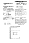
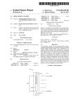
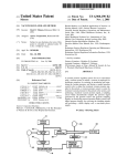
US006795911B1
(12) United States Patent
(10) Patent N0.:
US 6,795,911 B1
(45) Date of Patent:
Sep. 21, 2004
Miyano
(54)
COMPUTING DEVICE HAVING
INSTRUCTIONS WHICH ACCESS EITHER A
5,895,481 A *
5,937,199 A *
6,260,101 B1 *
PERMANENTLY FIXED DEFAULT MEMORY
BANK OR A MEMORY BANK SPECIFIED BY
AN IMMEDIATELY PRECEDING BANK
SELECTION INSTRUCTION
(75) Inventor: T0m0mi Miyano, Miyazaki (JP)
FOREIGN PATENT DOCUMENTS
JP
7-191906
JP
7-234818
9/1995
JP
7'325757
12/1995
7/1995
OTHER PUBLICATIONS
(73) Assignee: Oki Electric Industry Co., Ltd., Tokyo
(JP)
4/1999 Yap ............................. .. 711/5
8/1999 Temple ........ ..
710/262
7/2001 Hansen et al. .............. .. 710/22
Intel Corporation, iAPX 86/88, 186/188 User’s Manual—
Hardware Reference, 1985, pp. 1—1 and 1—7 to 1—10.*
(*) NOtiCéI
subject'to any diSClaiIIlfIr,~ the term Of this
Harvey, RE, 8086 Processor Registers, http://web.archi
patent 1S eXIended 0r adjusted under 35
ve.org/web/19991111090421/http://ourworld.compuserve
U.S.C. 154(b) by 0 days.
.com/homepages/riharvey/docicpu.htm, 1999*
*
(21) Appl. N0.: 09/493,157
(22) Filed:
(51)
Jam 28’ 2000
.
Primary Examiner—Eddie Chan
Int. Cl.7 .......................... .. G06F 12/00; G06F 9/00
(52) US. Cl. ..................... .. 712/225; 712/208; 7127/2285;
of Search ............................... ..
Assistant Examiner—David J. Huisman
(74) Attorney, Agent, or Firm—Volentine Francos, PLLC
(57)
ABSTRACT
A computing device accesses
712/208; 711/5, 157, 148, 173
_
(56)
.
‘med by exammer
memory banks,
which are selected by a bank selection instruction. The
memory bank selected by the bank selection instruction is
References Clted
accessed by a memory access instruction immediately fol
U~S_ PATENT DOCUMENTS
lowing ' the bank selection instruction. Following any
instruction other than the bank selection instruction, a
4,028,675 A *
6/ 1977 Frankenberg ------------- -- 365/222
default memory bank is selected automatically. This scheme
45277261 A
7/1985
eliminates
:
Smlther - - - - - - - - - -
- - - - ~~
333/12
4,601,018 A
5’OO1’626 A *
7/1986 Balm} et a1‘ """"""" " 365/200
3/1991 Kashlyama et a1‘ """"" " 712/4
5,193,169 A
3/1993
*
5,655,099 A *
5,751,988 A *
Ishikawa
............. ..
the
need
to
select
the
default memory bank
explicitly, and the need to save and restore the contents of a
bank selection register when interrupts are served
710/22
'
8/1997 Bjerge et al.
711/2
5/1998 Fujimura .................. .. 711/220
8 Claims, 4 Drawing Sheets
5
2
f
I
‘,3
REGISTER
1o
BANK
4.\__
A0 —A15
A1s-A19
BANK
A16-A19
COL'I'JEOL
16
INSTRUCTION
OOOOOH
10000H
BANK
0
BANK
1
7000OH
MEMORY
I
""
BANK
7
INSTRUCTION DECODER
I
6
L
ACCUMULATOR
S
14
I
,
OFFFFH 1FFFFH
vo
PORT
#
7FFFFH
J
12
Do-D15
U.S. Patent
Sep. 21, 2004
Sheet 1 014
US 6,795,911 B1
FIG. 1
OOOOH
A
BANKO
FFFFH
OOOOH
BANK1
FFFFH
OOOOH
BANK2
FFFFH
OOOOH
BANK3
FFFFH
64 KBYTES x 8 BANKS
OOOOH
BANK4
FFFFH
OOOOH
BANKS
FFFFH
OOOOH
BANK6
FFFFH
OOOOH
BANK?
FFFFH
,
U.S. Patent
Sep. 21, 2004
Sheet 3 014
US 6,795,911 B1
FIG. 3
1
3°
L 8
CK
CLR
BEN
CLK '__'—
BDIS
28
24
A16-A19
26
/
A16'A19
US 6,795,911 B1
1
2
COMPUTING DEVICE HAVING
INSTRUCTIONS WHICH ACCESS EITHER A
PERMANENTLY FIXED DEFAULT MEMORY
BANK OR A MEMORY BANK SPECIFIED BY
AN IMMEDIATELY PRECEDING BANK
SELECTION INSTRUCTION
The invented method of selecting a memory bank
includes the steps of:
selecting a memory bank speci?ed by a bank selection
instruction for use by the next instruction executed after the
bank selection instruction; and
automatically selecting a predetermined default memory
bank folloWing execution of any instruction other than the
bank selection instruction.
BACKGROUND OF THE INVENTION
The invented computing device has a bank register storing
The present invention relates to a computing device such
a value specifying one of a plurality of memory banks, and
as a microprocessor employing a memory divided into
a bank control unit operating in a ?rst state and a second
banks.
state. In the ?rst state, the bank control unit selects the
Microprocessors capable of addressing multiple memory
banks are Well knoWn in the computing art. The instruction
set of a microprocessor of this type includes a bank selection
instruction that sets a bank address in a bank register.
Memory access instructions specify addresses that can apply
15
memory bank speci?ed by the bank register. In the second
state, the bank control unit selects the predetermined
memory bank.
BRIEF DESCRIPTION OF THE DRAWINGS
to any bank. When a memory access instruction is executed,
In the attached draWings:
the address speci?ed in the instruction is combined With the
value in the bank register to generate an address specifying
both a particular memory bank and a particular location in
that memory bank.
If the softWare running on the microprocessor is of the
FIG. 1 illustrates a memory divided into banks;
FIG. 2 is a block diagram of a microprocessor embodying
the present invention;
FIG. 3 is a more detailed block diagram of the bank
multitasking type, different tasks or processes may use
different memory banks. Typically, each process begins With
25
a bank selection instruction that sets the address of the
cessor.
desired bank in the bank register. If necessary, the bank
selection instruction can be executed again during the pro
DETAILED DESCRIPTION OF THE
INVENTION
cess to sWitch banks. If one process interrupts another, the
bank register contents are saved onto a stack, and restored
An embodiment of the invention Will be described With
reference to the attached draWings, in Which like parts are
When the interrupting process ends, so that the interrupted
process can resume use of the correct bank.
indicated by like reference characters.
FIG. 1 illustrates a memory divided into eight banks,
An advantage of this scheme is that the memory address
space can be expanded beyond the siZe that can be addressed
by any one memory access instruction, Without increasing
the bit length of the memory access instructions.
numbered from Zero to seven. Each memory bank has
addresses from OOOOH to FFFFH, the H suf?x indicating
hexadecimal notation. These addresses are speci?ed by
sixteen address bits. Each memory bank has a capacity of
A disadvantage, hoWever, is that saving and restoring the
contents of the bank register delays the sWitchover from one
process to the other. This is a particular disadvantage in
40
real-time control systems requiring quick response to inter
sixty-four kilobytes.
FIG. 2 shoWs a microprocessor 1 embodying the present
invention, using the bank memory shoWn in FIG. 1. The
microprocessor 1 comprises a processing unit 2 With an
rupts.
A further disadvantage is that every process must set the
bank register to be sure that memory accesses Will be
directed to the correct bank. There may be, for example,
many short processes that use only one memory bank, all
sharing the same memory bank. Each of these processes
must still start by executing the bank selection instruction,
control unit in FIG. 2; and
FIG. 4 is a block diagram of a conventional micropro
internal instruction memory 4, an instruction decoder 6, a
45
bank register 8, a bank control unit 10, a data input/output
(I/O) port 12, an accumulator 14, and various other facilities
(not visible). The processing unit 2 is coupled to the eight
memory banks 16 by an address bus carrying sixteen address
bits A0 to A15, an additional address bus carrying four more
address bits A16 to A19, and a data bus carrying sixteen
Which adds an unnecessary instruction to the process code
and further delays the start of the process.
parallel data bits D0 to D15. The tWenty address bits from A0
to A19 have values from OOOOOH to OFFFFH, identifying
These disadvantages could be overcome by adding bank
selection bits to the memory access instructions, enabling
be incompatible With existing instruction sets, requiring
locations in memory bank Zero, through 70000H to
7FFFFH, identifying locations in memory bank seven. The
memory banks 16 are part of the microprocessor I, prefer
ably being integrated onto the same semiconductor substrate
as the processing unit 2.
Incidentally, the term ‘microprocessor’ as used herein also
includes computing devices that are commonly referred to as
much conversion of existing softWare.
microcomputers and microcontrollers.
each memory access instruction to specify both a memory
bank and a location in the memory bank, but that Would be
a highly inefficient solution. Code siZe Would be greatly
increased, and extra circuits Would be needed to analyZe the
55
added instruction bits, increasing the siZe and cost of the
microprocessor itself. The expanded instructions Would also
The instruction decoder 6 decodes instructions received
SUMMARY OF THE INVENTION
An object of the present invention is to enable a comput
ing device to access multiple memory banks Without requir
ing all processes to execute bank selection instructions.
Another object is to eliminate the saving and restoring of
bank register contents.
65
from the instruction memory 4, supplies address bits A0 to
A15 to the memory banks, supplies address bits A16 to A19
to the bank register 8, and controls the bank control unit 10.
The bank control unit 10 receives address bits A16 to A19
from the bank register 8 and supplies either the received
address bits or four bits having a ?xed value of OH to the
US 6,795,911 B1
3
4
memory banks 16, depending on signals received from the
instruction decoder 6. The four bits A16 to A19 output by the
interval, the selector 28 selects the grounded inputs and
supplies an A16—A19 address value of 0H, selecting bank
bank control unit 10 select one of the memory banks 16.
Zero.
Three bits Would be adequate, since there are only eight
banks, but four bits give the microprocessor 1 the capability
The bank designated by the bank register 8 is thus selected
only during the execution of the next instruction folloWing
to address up to sixteen memory banks. The other sixteen
each bank selection instruction. At other times, bank Zero is
address bits A0 to A15 specify a location in the memory bank
selected regardless of the contents of the bank register 8.
Consequently, absent an immediately preceding bank selec
selected by bits A16 to A19.
tion instruction, a memory access instruction accesses
FIG. 3 shoWs the internal structure of the bank control
unit 10, Which comprises a set-reset ?ip-?op 20, a pair of
AND gates 22, 24, an inverter 26, and a selector 28. The
signals received by the bank control unit 10 include a bank
output enable signal (BEN), Which is input by the ?rst AND
gate 22; a clock signal (CLK), input by both AND gates 22,
24; a bank output disable signal (BDIS), input by the second
10
tion decoder 6 specify sixteen-bit memory addresses, Which
the instruction decoder places on the AO—A15 address bus
signal lines. These sixteen-bit addresses indicate locations in
15
AND gate 24; and address bits A16 to A119, Which are input
by the selector 28. The output terminal of the ?rst AND gate
22 is coupled to the clock (CK) input terminal of the
set-reset ?ip-?op 20. The output terminal of the second AND
gate 24 is coupled through inverter 26 to the clear (CLR)
input terminal of the set-reset ?ip-?op 20. The data input
terminal (D) and set input terminal (S) of the set-reset
?ip-?op 20 are coupled to the poWer supply, thus being held
Zero. If immediately preceded by a bank selection
instruction, the memory access instruction accesses the
memory bank speci?ed in the bank selection instruction.
A memory access transfers data on the data bus lines D0
to D15 betWeen the selected memory bank 16 and, for
example, the accumulator 14, the data passing through the
25
data input/output port 12. Data can also be transferred
betWeen the selected memory bank and other facilities (not
visible) in the processing unit 2.
Memory bank Zero preferably includes memory-mapped
special-function registers, memory-mapped input-output
When the Q output of the set-reset ?ip-?op 20 is high (‘1’),
ports, the interrupt vector table, and other frequently
accessed addresses. In typical applications, many processes
the selector 28 selects the A16—A19 address bits received
from the bank register 8. When the Q output of the set-reset
Will need to access only memory bank Zero. These processes
?ip-?op 20 is loW (‘0’), the selector 28 selects the grounded
(‘0’) inputs. The selected inputs of the selector 28 become
the output address bits A16—A19 supplied by the bank control
can be coded using only standard memory-access instruc
tions specifying sixteen-bit addresses, Without any bank
unit 10 to the memory banks 16.
Next, the operation of this microprocessor 1 Will be
all eight memory banks 16, Without specifying Which
memory bank is to be accessed, but there is no ambiguity. By
default, a memory access instruction accesses memory bank
at the high (‘1’) logic level. The data output (Q) terminal of
the set-reset ?ip-?op 20 is coupled to the selector 28. The set
and clear inputs S and CLR are active loW.
The selector 28 also has a set of grounded input terminals.
memory bank Zero by default.
The memory access instructions decoded by the instruc
35
selection instructions at all. The code siZe and execution
time of these processes are thereby reduced.
Processes that access other memory banks require a
separate bank selection instruction each time a bank other
described.
The microprocessor 1 has a conventional instruction set
With a bank selection instruction that Writes desired values
than bank Zero is accessed, even When the same bank is
of address bits A16 to A19 into the bank register 8. The bank
disadvantage, the disadvantage is offset by the advantage
accessed repeatedly. While this requirement is a
40
selection instruction also disables interrupts for one instruc
tion execution cycle, so that an interrupt received during the
execution of the bank selection instruction is not recogniZed
until after the next instruction has been executed.
Upon decoding the bank selection instruction, besides
sending address bits A16 to A19 to the bank register 8, the
that these processes can sWitch from another bank to bank
Zero Without having to execute a bank selection instruction.
Afurther advantage of the invented microprocessor is that
When one process interrupts another, the bank register
45
instruction decoder 6 sets the bank enable signal BEN to the
high level and the bank disable signal BDIS to the loW level.
The clear input terminal of the set-reset ?ip-?op 20 is
selection instruction, the memory access instruction to
Which the bank selection instruction applies is executed
before the interrupt is served, so the interrupt-handling
process can alter the bank register contents With impunity.
thereby set to the inactive (high) level, and input of the clock
signal CLK to the clock input terminal CK is enabled.
During the next clock cycle, the high logic level that is
constantly received at the data input terminal D is latched in
the set-reset ?ip-?op 20, in synchroniZation With the clock
signal, causing the Q output signal to go high, thereby
Eliminating the saving and restoring of the bank register is
a signi?cant advantage in real-time control applications.
A further advantage is that the invented microprocessor
55
causing the selector 28 to select the A16—A19 address values
received from the bank register 8.
Upon decoding any instruction other than the bank selec
tion instruction, the instruction decoder 6 sets the bank
enable signal BEN to the loW level at, for example, the
beginning of the instruction execution cycle, and sets the
bank disable signal BDIS to the high level at the end of the
instruction execution cycle. The signal output from inverter
26 goes loW for the duration of one high CLK pulse, thereby
clearing the set-reset ?ip-?op 20 and forcing the Q output
signal to go loW. The Q output signal remains loW until the
next bank selection instruction is executed. Throughout this
contents do not have to be saved and restored. Even if an
interrupt request is received during the execution of a bank
operates efficiently regardless of Whether or not there are
multiple memory banks, and enables the number of banks to
be expanded from one to more than one Without requiring
modi?cations to existing softWare. An operating system and
other programs coded for a single-bank environment can be
used Without change in a multiple-bank environment.
For comparison, FIG. 4 shoWs a conventional micropro
cessor 30 With multiple memory banks. The conventional
microprocessor 30 has the structure shoWn in FIG. 2,
Without the bank control unit. The bank register 8 is alWays
65
used to select the memory bank, so even instructions that
access bank Zero must be preceded by a bank selection
instruction, and the bank register contents must be saved and
restored at interrupts.
US 6,795,911 B1
5
6
The invention is not limited to the embodiment described
above. For example, the memory banks need not all be
banks, the computing device also having an instruction set
integrated into the microprocessor. External memory banks
tion instruction, the computing device further having a bank
register storing a value specifying an arbitrary one of the
that includes memory access instructions and a bank selec
can be accessed in the same Way.
plurality of mutually exclusive memory banks, the comput
The structure of the bank control unit shoWn in FIG. 3 can
be modi?ed in various Ways. For example, the second AND
gate 24 and inverter 26 can be replaced by a NAND gate.
The set-reset ?ip-?op 20 can be replaced by any type of
ing device generating an address upon execution of each
memory access instruction, the address being divided into a
?rst part and a second part, the ?rst part and the second part
bi-stable circuit that can be sWitched betWeen tWo states.
Those skilled in the art Will recogniZe that further varia
tions are possible Within the scope claimed beloW.
What is claimed is:
10
1. A method of selecting a memory bank for access by a
computing device having a memory permanently divided
into a plurality of mutually exclusive memory banks, the
being mutually exclusive, the ?rst part including at least one
?rst address bit for selecting an arbitrary one of the plurality
of mutually exclusive memory banks, and the second part
including a plurality of second address bits for specifying
addresses Within the arbitrary selected memory bank, the
computing device comprising:
a bank control unit operating in a ?rst state and a second
computing device also having an instruction set that includes
state, Wherein in the ?rst state the bank control unit sets
said ?rst part of the address to the value stored in said
memory access instructions and a bank selection instruction,
the computing device generating an address upon execution
of each memory access instruction, the address being
divided into a ?rst part and a second part, the ?rst part and
bank register to select the memory bank speci?ed by
the second part being mutually exclusive, the ?rst part
bank control unit sets said ?rst part of the address to a
including at least one ?rst address bit for selecting the
memory bank from among the plurality of mutually exclu
sive memory banks, and the second part including a plurality
permanently ?xed value to select a permanently ?xed
one of the memory banks,
Wherein said bank control unit operates in said ?rst state
of second address bits used in common for specifying
addresses Within any selected one of the plurality of mutu
upon execution of each memory access instruction
Which folloWs a the bank selection instruction, and
ally exclusive memory banks, the method comprising the
steps of:
Wherein said bank control unit operates in said second
the bank register, and Wherein in the second state the
state upon execution of each memory access instruction
Which does not folloW a the bank selection instruction.
(a) upon execution of each memory access instruction
Which folloWs a bank selection instruction, setting said
5. The computing device of claim 4, Wherein the bank
selection instruction sets said value in the bank register,
?rst part of the address generated by the computing
further comprising:
device according to the bank selection instruction to
select the memory bank speci?ed by the bank selection
instruction, and accessing the speci?ed memory bank
according to the executed memory access instruction;
and
(b) upon execution of each memory access instruction
Which does not folloW a bank selection instruction,
automatically setting said ?rst part of the address
generated by the computing device to a permanently
35
40
?xed value to select a permanently ?xed default
memory bank, and accessing the default memory bank
according to the executed memory access instruction.
2. The method of claim 1, Wherein said step (a) further
comprises the steps of:
storing a value speci?ed by the bank selection instruction
45
6. The computing device of claim 4, Wherein the bank
control unit comprises:
a bi-stable circuit generating a ?rst control value in the
?rst state and a second control value in the second state;
and
a selector coupled to the bi-stable circuit, having a ?rst
input terminal receiving the value stored in the bank
register and a second input terminal receiving said
permanently ?xed value, selecting the ?rst input ter
minal When the bi-stable circuit generates the ?rst
control value, selecting the second input terminal When
the bi-stable circuit generates the second control value,
and supplying the value received at the selected input
in a bank register;
setting a bi-stable circuit to a ?rst state When the bank
selection instruction is executed; and
setting said ?rst part of the according to the value stored
in the bank register When the bi-stable circuit is in the
?rst state;
terminal to the memory banks as said ?rst part of the
address.
and said step (b) further comprises the steps of:
7. The computing device of claim 4, Wherein the com
puting device is a microprocessor.
8. The computing device of claim 5, Wherein the instruc
setting the bi-stable circuit to a second state folloWing
said execution of each instruction other than the bank
selection instruction; and
setting said ?rst part of the address to said permanently
tion decoder sends the bank control unit a ?rst signal and a
second signal, the ?rst signal setting the bank control unit to
the ?rst state, the second signal setting the bank control unit
to the second, the ?rst signal being output When the bank
selection instruction is decoded, the second signal being
?xed value When the bi-stable circuit is in the second
state.
3. The method of claim 1, further comprising the step of
disabling interrupts during the execution of the bank selec
output When any instruction other than the bank selection
instruction is decoded.
tion instruction.
4. A computing device having a memory permanently
divided into a plurality of mutually exclusive memory
an instruction decoder decoding the instructions in the
instruction set, setting the bank control unit to the ?rst
state When the bank selection instruction is decoded,
and setting the bank control unit to the second state
folloWing execution of each instruction other than the
bank selection instruction in the instruction set.
65