1
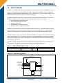
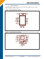
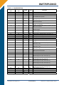
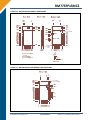
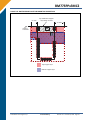
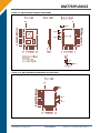
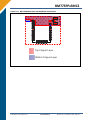
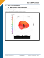
30077 新竹科學工業園區工業東七路5號5樓 5F, No.5, Industry E. Rd. VII, Hsinchu Science Park, Hsinchu 30077, Taiwan, R.O.C. TEL : 886-3-577-8385 FAX : 886-3-577-8945 www.issc-tech.com BM77SPPx3MC2 Bluetooth® 4.0 Dual Mode Module Features: FIGURE 1: Complete, Fully Certified, Embedded 2.4 GHz Bluetooth® Version 4.0 Module Bluetooth Classic (BR/EDR) and Low Energy (LE) Bluetooth SIG Certified Onboard embedded Bluetooth Stack Transparent UART mode for seamless serial data over UART interface Easy to configure with Windows GUI or direct by MCU Firmware can be field upgradable via UART Compact surface mount module: 22 x 12 x 2.4 mm Castellated surface mount pads for easy and reliable host PCB mounting Environmentally friendly, RoHS compliant Perfect for Portable Battery Operated Devices Internal Battery Regulator Circuitry Worldwide regulatory certifications Operational: Single operating voltage: 3.2V to 4.3V Temperature range: ‐40C to 85C Industrial Simple, UART interface Integrated crystal, internal voltage regulator, and matching circuitry Multiple I/O pins for control and status General Description: Frequency: 2.402 to 2.480 GHz Receive Sensitivity: ‐90 dBm (Classic); ‐92 dBm (LE) Power Output: 2 dBm (typ.) Data Throughput: 3 Mbps (Classic) 8 Kbps (LE) MAC/Baseband/Higher Layer: Secure AES128 encryption GAP, SDP, SPP, GATT profiles Antenna: Ceramic Chip Antenna (BM77SPPS3MC2) External Antenna Connection via RF Pad (BM77SPP03MC2) The BM77 is a fully‐certified Bluetooth® Version 4.0 (BR/EDR/LE) module for designers who want to easily add dual mode Bluetooth® wireless capability to their products. Delivering local connectivity for the Internet of Things (IoT), the BM77 bridges your product to Smart Phones and Tablets for convenient data transfer, control and access to cloud applications. This Bluetooth SIG certified module provides a complete wireless solution with Bluetooth stack onboard, integrated antenna, and worldwide radio certifications in a compact surface mount package, 22 x 12 x 2.4 mm. It supports GAP, SDP, SPP, and GATT profiles. Data is transferred over the Bluetooth link by sending/receiving data via transparent UART mode, making it easy to integrate with any processor or Microcontroller with a UART interface. Configuration is made easy using a Windows® based GUI or directly via UART by a MCU. Applications: Compliance: Bluetooth SIG QDID: B021961 Modular Certified for the United States (FCC) and Canada (IC) European R&TTE Directive Assessed Radio Module Australia, New Zealand, Korea, Taiwan, Japan © 2014 ISSC Technologies Corp. RF/Analog: Mobile Point of Sales (mPOS) LED lighting Wearables Digital Sports Fitness Devices Health Care/ Medical Automotive Accessories Home Automation Remote Control Toys Preliminary Revision 2.0 – October 24, 2014 Page 1 1.0 BM77SPPx3MC2 DEVICE OVERVIEW The BM77 is a complete, fully certified, embedded 2.4 GHz Bluetooth® version 4.0 (BR/EDR/LE) wireless module. It incorporates an on‐board Bluetooth stack, cryptographic accelerator, power management subsystem, 2.4 GHz transceiver, and RF power amplifier (see Figure 1‐1). With the BM77, designers can embed Bluetooth functionality rapidly into virtually any device. The BM77 provides cost and time‐to‐market savings as a self‐contained module solution. The module has been designed to provide integrators with a simple Bluetooth solution that features: Ease of integration and programming Vastly reduced development time Minimum system cost Interoperability with Bluetooth hosts Maximum value in a range of applications The BM77 can independently maintain a low‐power wireless connection. Low‐power usage and flexible power management maximize the module’s lifetime in battery‐operated devices. A wide operating temperature range allows use in indoor and outdoor environments (industrial temperature range). The BM77 module comes in two varieties. The BM77SPPS3MC2 is a complete, fully regulatory certified module with integral ceramic chip antenna and shield. The BM77SPP03MC2 is a lower cost alternative with external antenna and no shield. The integrator is responsible for the antenna, antenna matching, and regulatory certifications. The BM77 is a small, compact, surface mount module with castellated pads for easy and reliable host PCB mounting. The module is compatible with standard pick‐and‐place equipment. TABLE 1‐1: BM77 MODULE FAMILY TYPES Device BM77SPPS3MC2‐0007AA BM77SPP03MC2‐0007AA Antenna Integral ceramic chip External Shield Yes No Regulatory Certifications FCC, IC, CE, KCC, NCC, Japan CE FIGURE 1‐1: BM77 BLOCK DIAGRAM BM77SPPx3MC2 Ceramic Chip Antenna (BM77SPPS3MC2) External Antenna (BM77SPP03MC2) IS1677SM 16 MHz RF Matching Configurable Control and Indication I/O UART Power I2C 8Kbit Serial EEPROM © 2014 ISSC Technologies Corp. Preliminary Revision 2.0 – October 24, 2014 Page 2 1.1 BM77SPPx3MC2 Interface Description The BM77SPPS3MC2 pin diagram is shown in Figure 1‐2 and the BM77SPP03MC2 is shown in Figure 1‐3. The pin descriptions are shown in Table 1‐1 FIGURE 1‐2: BM77SPPS3MC2 PIN DIAGRAM FIGURE 1‐3: BM77SPP03MC2 PIN DIAGRAM © 2014 ISSC Technologies Corp. Preliminary Revision 2.0 – October 24, 2014 Page 3 BM77SPPx3MC2 TABLE 1‐1: PIN DESCRIPTION BM77SPPS3MC2 Pin 1 2 3 4 BM77SPP03MC2 Pin ‐‐ ‐‐ 1 2 5 Symbol Type Description GND GND GND BAT_IN Power Power Power Power 3 SW_BTN DI 6 4 LDO33_O Power 7 5 VDD_IO Power 8 6 LDO18_O Power 9 7 WAKEUP DI 10 8 PMULDO_O Power 11 12 13 14 15 16 17 9 10 11 12 13 14 15 P04 P15 P12/SCL P13/SDA P17/CTS P05 P00/RTS DO DO DO DIO DIO DIO DIO 18 16 P20 DI 19 17 P24 DI 20 18 EAN DI 21 19 RST_N DI 22 23 24 20 21 22 RXD TXD P31 DI DO DIO 25 23 P32 DIO 26 24 P33 DIO 27 25 P34 DIO 28 29 26 27 P36 P37 DIO DIO 30 31 ‐‐ 32 33 28 29 30 ‐‐ ‐‐ LED1 GND BT_RF GND GND DO Power AIO Power Power Ground reference Ground reference Ground reference Battery Input. Main positive supply input. Connect to 10 uF low ESR ceramic capacitor. Software Button H: Power On / L: Power Off (See Section 1.6) Internal 3.3V LDO regulator output. Connect to 10 uF low ESR ceramic capacitor. I/O positive supply input. Ensure VDD_IO and MCU I/O voltages are compatible. Internal 1.8V LDO regulator output. Connect to 10 uF low ESR ceramic capacitor. Wakeup from shutdown mode (active low) (internal pull‐up) Power management unit output. Connect to 1 uF low ESR ceramic capacitor. Status Indicator 2 (STATUS_IND_2). See Section 1.5 Status Indicator 1 (STATUS_IND_1). See Section 1.5 I2C SCL (Do Not Connect) I2C SDA (Do Not Connect) Configurable Control or Indication pin or UART CTS (input) Configurable Control or Indication pin Configurable Control or Indication pin or UART RTS (output) System configuration (internal pull‐up) (See Section 1.10) System configuration (internal pull‐up) (See Section 1.10) System configuration (internal pull‐down) (See Section 1.10) Module reset (active low) (internal pull‐up) Apply a pulse of at least 63 ns. UART data input UART data output Configurable Control or Indication pin (when configured as input: internal pull‐up) Configurable Control or Indication pin (when configured as input: internal pull‐up) Configurable Control or Indication pin (when configured as input: internal pull‐up) Configurable Control or Indication pin (when configured as input: internal pull‐up) (Do Not Connect) Configurable Control or Indication pin (when configured as input: internal pull‐up) Status LED (See Section 1.9) Ground reference External antenna connection (50 ohm) Ground reference Ground reference Note 1: Pin type abbreviation: A = Analog, D = Digital, I = Input, O = Output. © 2014 ISSC Technologies Corp. Preliminary Revision 2.0 – October 24, 2014 Page 4 BM77SPPx3MC2 1.2 Configuring the BM77 Configuring the BM77 features can be performed using either MCU commands documented in the “ISSC Flash Protocol Programmer’s Guide,” or with the “Windows UI Configuration tool” and “Write EEPROM tool.” MCU UART commands are documented in “BM77SPP Command Set.” 1.3 UART Interface Figures 1‐4 and 1‐5 show Power and MCU interface examples. The BM77 UART pins TXD and RXD connect to the UART pins of the host MCU. It is highly recommended to use hardware flow control pins RTS and CTS. The BM77 hardware flow control is disabled by default and must be configured to enable. The UART Baud is configurable. The available signal rates are listed in Table 4‐5. 1.4 Control and Indication I/O Pins DISCOVERY_CONTROL PROFILE_IND Default UART_RX_IND DISCONNECT_CONTROL LINK_QUALITY_IND LOW_BATTERY_IND UART_CTS Default Default Default Default Default Default INQUIRY CONTROL P00 P05 P17 P31 P32 P33 P34 P37 UART_RTS N/C I/O pins P00, P05, P17, P31, P32, P33, P34 and P37 are configurable control and indication I/O. Control signals are input to the BM77. Indication signals are output from the BM77. Table 1‐2 shows configurable I/O pin assignment to control and indication signals. Note that RTS can only be assigned to P00 and CTS to P17. TABLE 1‐2: CONFIGURATION AND INDICATION I/O ASSIGNMENTS Default 1.5 Status Indication I/O Pins I/O pins P15 and P04 are Status Indicator 1 and 2 signals respectively. Together they provide status indication to the MCU as shown in Table 1‐3. TABLE 1‐3: STATUS INDICATION P04/STATUS_IND_2 H H L L © 2014 ISSC Technologies Corp. P15/STATUS_IND_1 H L H L Indication Power default / Shutdown state Access state Link state (no UART data being transmitted) Link state (UART data being transmitted) Preliminary Revision 2.0 – October 24, 2014 Page 5 1.6 BM77SPPx3MC2 Software Button (SW_BTN) The Software Button (SW_BTN) input pin powers the BM77 on (high) or off (low) 1.7 WAKE UP (WAKEUP) The Wake Up (WAKEUP) input pin wakes the BM77 from shutdown mode (active low). 1.8 RESET (RST_N) The Reset (RST_N) input pin resets the BM77 (active low pulse for at least 63 ns). 1.9 Status LED (LED1) The status LED (LED1) indicates: Standby Inquiry Link Link Back Low Battery Page Each indication is a configurable flashing sequence. LED brightness can also be configured. 1.10 System Configuration I/O pins P20, P24, and EAN place the BM77 into operation modes as shown in Table 1‐4. P20 and P24 each have internal pull‐ups. EAN has internal pull‐down. TABLE 1‐4: SYSTEM CONFIGURATION SETTINGS P20 P24 EAN Operational Mode High High Low Normal operation Low High Low Test (Write EEPROM) Low Low High Write Flash (Firmware programming) 1.11 Power Figure 1‐4 shows an example power scheme using a 3.3 volt low‐dropout (LDO) regulator supplying 3.3 volts to both the BM77 (BAT_IN and VDD_IO) and MCU VDD. This power scheme ensures that BM77 and MCU I/O voltages are compatible. Figure 1‐5 shows an example power scheme using a 3.7 volt lithium‐ion battery. The BM77 has an internal 3.3 volt LDO regulator. Battery power is applied to BAT_IN pin. The regulated 3.3 volts output is on the LDO33_O pin. From the LDO33_O pin, voltage can be routed the VDD_IO pin and external circuitry including the MCU. This power scheme ensures that BM77 and MCU I/O voltages are compatible. CAUTION: The internal 3.3 volt LDO current source: 50 mA maximum Recommended bypass capacitor location and values are shown in Figures 1‐4 and 1‐5. Capacitors can be low ESR ceramic. Place capacitors close to BM77 module. © 2014 ISSC Technologies Corp. Preliminary Revision 2.0 – October 24, 2014 Page 6 BM77SPPx3MC2 FIGURE 1‐4: BM77 TO MCU INTERFACE EXAMPLE – LDO P20 P24 EAN FIGURE 1‐5: BM77 TO MCU INTERFACE EXAMPLE – BATTERY Li-ion Battery (3.7V) LDO (3.3V) BM77 Module BAT_IN (3.2 – 4.3V) 10uF MCU P15/STATUS_IND_1 P04/STATUS_IND_2 I/O I/O SW_BTN WAKEUP RST_N I/O I/O I/O P37 P34 P33 P32 P31 P05 I/O I/O I/O I/O I/O I/O LDO33_O 10uF VDD_IO (Note 1) (2.8 – 3.63V) NC LDO18_O Note 2 PMULDO_O RX TX TXD RXD P20 P24 EAN LED1 P12/SCL P13/SDA P36 System Configuration © 2014 ISSC Technologies Corp. Note 1 CTS RTS P00/RTS P17/CTS NC VDD NC NC NC Note: 1. Ensure VDD_IO and MCU VDD voltages are compatible. 2. Control and indication ports are configurable. Preliminary Revision 2.0 – October 24, 2014 Page 7 1.12 BM77SPPx3MC2 Mounting Details The BM77SPPS3MC2 physical dimensions are shown in Figure 1‐6, recommended host PCB footprint in Figure 1‐7, and mounting suggestion in Figure 1‐8. There should not be top copper layer near the test pin area shown in Figure 1‐7. When laying out the host PCB, the areas under the antenna should not contain any top, inner layer, or bottom copper as shown in Figure 1‐8. A low‐impedance ground plane will ensure best radio performance (best range, lowest noise). Figure 1‐8 shows a minimum ground plane area to the left and right of the module for best antenna performance. The ground plane can be extended beyond the minimum recommended as need for host PCB EMC noise reduction. For best range performance, keep all external metal away from the ceramic chip antenna at least 31 mm. The BM77SPP03MC2 physical dimensions are shown in Figure 1‐9, recommended host PCB footprint in Figure 1‐10, and mounting suggestion in Figure 1‐11. It is highly recommended to layout the host PCB as suggested in Figure 1‐11. A low‐impedance ground plane will ensure best radio performance (best range, lowest noise). Pin 30 (BT_RF) is a 50 ohm connection to an external antenna connector, PCB trace antenna, or component (ceramic chip) antenna through a host PCB 50 ohm micro‐strip trace. This trace can be extended to include passive parts for antenna attenuation padding, impedance matching, or to provide test posts. It is recommended that the micro‐strip trace be as short as possible for minimum loss and best impedance matching. If the micro‐strip trace is longer, it should be a 50 ohm impedance. Figure 1‐11 shows an example connection to U.FL connector. 1.13 Soldering Recommendations The BM77 wireless module was assembled using standard lead‐free reflow profile IPC/JEDEC J‐STD‐020. The module can be soldered to the host PCB using standard leaded and lead‐free solder reflow profiles. To avoid damaging the module, the following recommendations are given: Microchip Technology Application Note AN233 Solder Reflow Recommendation (DS00233) provides solder reflow recommendations Do not exceed peak temperature (TP) of 250 deg C Refer to the solder paste data sheet for specific reflow profile recommendations Use no‐clean flux solder paste Do not wash as moisture can be trapped under the shield Use only one flow. If the PCB requires multiple flows, apply the module on the final flow. © 2014 ISSC Technologies Corp. Preliminary Revision 2.0 – October 24, 2014 Page 8 BM77SPPx3MC2 FIGURE 1‐6: BM77SPPS3MCS MODULE DIMENSIONS FIGURE 1‐7: BM77SPPS3MC2 RECOMMEDED PCB FOOTPRINT © 2014 ISSC Technologies Corp. Preliminary Revision 2.0 – October 24, 2014 Page 9 BM77SPPx3MC2 FIGURE 1‐8: BM77SPPS3MCS HOST PCB MOUNTING SUGGESTION >4.7mm Top and Bottom Copper layer keep out area >6.4mm Edge of host PCB Top Copper Layer Bottom Copper Layer © 2014 ISSC Technologies Corp. Preliminary Revision 2.0 – October 24, 2014 Page 10 BM77SPPx3MC2 FIGURE 1‐9: BM77SPP03MCS MODULE DIMENSIONS FIGURE 1‐10: BM77SPP03MC2 RECOMMEDED PCB FOOTPRINT © 2014 ISSC Technologies Corp. Preliminary Revision 2.0 – October 24, 2014 Page 11 BM77SPPx3MC2 FIGURE 1‐11: BM77SPP03MCS HOST PCB MOUNTING SUGGESTION Top Copper Layer Bottom Copper Layer © 2014 ISSC Technologies Corp. Preliminary Revision 2.0 – October 24, 2014 Page 12 2.0 BM77SPPx3MC2 APPLICATION INFORMATION 2.2 BM77SPPS3MC2 Ceramic Chip Antenna The BM77SPPS3MC2 module contains an integral ceramic chip antenna. The antenna performance on the module is shown in Figure 2‐1. FIGURE 2‐1: BM77SPPS3MC2 ANTENNA RADIATION PATTERN Gain (dBi) 5.0 Y-ax is s ax i X- 0.0 -5.0 Z-axis -10.0 -15.0 -20.0 -25.0 -30.0 -35.0 Frequency Max Gain Efficiency 2450 MHz 1.63 dBi 71.55% © 2014 ISSC Technologies Corp. Preliminary Revision 2.0 – October 24, 2014 Page 13 BM77SPPx3MC2 2.3 External Configuration and Programming © 2014 ISSC Technologies Corp. RST_N P20 P24 EAN RTS/P00 P05 CTS/P17 The BM77 module can be configured and firmware programmed using an external configuration and programming tool available from ISSC Technologies. Figure 2‐2 shows the connections between the BM77 and header J1, a standard 8‐pin 0.100” (2.54 mm) spaced header. It is recommended to include this header on the host PCB for development. Configuration and firmware programming modes are entered according to the system configuration I/O pins (see Section 1.8). FIGURE 2‐2: EXTERNAL PROGRAMMING HEADER CONNECTIONS Preliminary Revision 2.0 – October 24, 2014 Page 14 3.0 BM77SPPx3MC2 REGULATORY APPROVAL This section outlines the regulatory information for the BM77SSPS3MC2 module for the following countries: United States Canada Europe Australia New Zealand Japan Korea Taiwan Other Regulatory Jurisdictions 3.2 United States The BM77SSPS3MC2 module has received Federal Communications Commission (FCC) CFR47 Telecommunications, Part 15 Subpart C “Intentional Radiators” modular approval in accordance with Part 15.212 Modular Transmitter approval. Modular approval allows the end user to integrate the BM77 module into a finished product without obtaining subsequent and separate FCC approvals for intentional radiation, provided no changes or modifications are made to the module circuitry. Changes or modifications could void the user’s authority to operate the equipment. The end user must comply with all of the instructions provided by the Grantee, which indicate installation and/or operating conditions necessary for compliance. The finished product is required to comply with all applicable FCC equipment authorizations regulations, requirements and equipment functions not associated with the transmitter module portion. For example, compliance must be demonstrated to regulations for other transmitter components within the host product; to requirements for unintentional radiators (Part 15 Subpart B “Unintentional Radiators”), such as digital devices, computer peripherals, radio receivers, etc.; and to additional authorization requirements for the non‐transmitter functions on the transmitter module (i.e., Verification, or Declaration of Conformity) (e.g., transmitter modules may also contain digital logic functions) as appropriate. 3.2.1 LABELING AND USER INFORMATION REQUIREMENTS The BM77 module has been labeled with its own FCC ID number, and if the FCC ID is not visible when the module is installed inside another device, then the outside of the finished product into which the module is installed must also display a label referring to the enclosed module. This exterior label can use wording as follows: Contains Transmitter Module FCC ID: A8TBM77SPPSYC2A or Contains FCC ID: A8TBM77SPPSYC2A This device complies with Part 15 of the FCC Rules. Operation is subject to the following two conditions: (1) this device may not cause harmful interference, and (2) this device must accept any interference received, including interference that may cause undesired operation © 2014 ISSC Technologies Corp. Preliminary Revision 2.0 – October 24, 2014 Page 15 BM77SPPx3MC2 A user’s manual for the finished product should include the following statement: This equipment has been tested and found to comply with the limits for a Class B digital device, pursuant to part 15 of the FCC Rules. These limits are designed to provide reasonable protection against harmful interference in a residential installation. This equipment generates, uses and can radiate radio frequency energy, and if not installed and used in accordance with the instructions, may cause harmful interference to radio communications. However, there is no guarantee that interference will not occur in a particular installation. If this equipment does cause harmful interference to radio or television reception, which can be determined by turning the equipment off and on, the user is encouraged to try to correct the interference by one or more of the following measures: Reorient or relocate the receiving antenna. Increase the separation between the equipment and receiver. Connect the equipment into an outlet on a circuit different from that to which the receiver is connected. Consult the dealer or an experienced radio/TV technician for help. Additional information on labeling and user information requirements for Part 15 devices can be found in KDB Publication 784748 available at the FCC Office of Engineering and Technology (OET) Laboratory Division Knowledge Database (KDB) http://apps.fcc.gov/oetcf/kdb/index.cfm. 3.2.2 RF EXPOSURE All transmitters regulated by FCC must comply with RF exposure requirements. KDB 447498 General RF Exposure Guidance provides guidance in determining whether proposed or existing transmitting facilities, operations or devices comply with limits for human exposure to Radio Frequency (RF) fields adopted by the Federal Communications Commission (FCC). From the FCC Grant: Output power listed is conducted. This grant is valid only when the module is sold to OEM integrators and must be installed by the OEM or OEM integrators. This transmitter is restricted for use with the specific antenna(s) tested in this application for Certification and must not be co‐located or operating in conjunction with any other antenna or transmitters within a host device, except in accordance with FCC multi‐transmitter product procedures. 3.2.3 HELPFUL WEB SITES Federal Communications Commission (FCC): http://www.fcc.gov FCC Office of Engineering and Technology (OET) Laboratory Division Knowledge Database (KDB): http://apps.fcc.gov/oetcf/kdb/index.cfm © 2014 ISSC Technologies Corp. Preliminary Revision 2.0 – October 24, 2014 Page 16 3.3 BM77SPPx3MC2 Canada The BM77SSPS3MC2 module has been certified for use in Canada under Industry Canada (IC) Radio Standards Specification (RSS) RSS‐210 and RSS‐Gen. Modular approval permits the installation of a module in a host device without the need to recertify the device. 3.3.1 LABELING AND USER INFORMATION REQUIREMENTS Labeling Requirements for the Host Device (from Section 3.2.1, RSS‐Gen, Issue 3, December 2010): The host device shall be properly labeled to identify the module within the host device. The Industry Canada certification label of a module shall be clearly visible at all times when installed in the host device, otherwise the host device must be labeled to display the Industry Canada certification number of the module, preceded by the words “Contains transmitter module”, or the word “Contains”, or similar wording expressing the same meaning, as follows: PENDING Contains transmitter module IC: 12246A‐BM77SPPSYC2 User Manual Notice for License‐Exempt Radio Apparatus (from Section 7.1.3 RSS‐Gen, Issue 3, December 2010): User manuals for license‐exempt radio apparatus shall contain the following or equivalent notice in a conspicuous location in the user manual or alternatively on the device or both: This device complies with Industry Canada license‐exempt RSS standard(s). Operation is subject to the following two conditions: (1) this device may not cause interference, and (2) this device must accept any interference, including interference that may cause undesired operation of the device. Le présent appareil est conforme aux CNR d'Industrie Canada applicables aux appareils radio exempts de licence. L'exploitation est autorisée aux deux conditions suivantes: (1) l'appareil ne doit pas produire de brouillage, et (2) l'utilisateur de l'appareil doit accepter tout brouillage radioélectrique subi, même si le brouillage est susceptible d'en compromettre le fonctionnement. © 2014 ISSC Technologies Corp. Preliminary Revision 2.0 – October 24, 2014 Page 17 BM77SPPx3MC2 Transmitter Antenna (from Section 7.1.2 RSS‐Gen, Issue 3, December 2010): User manuals for transmitters shall display the following notice in a conspicuous location: Under Industry Canada regulations, this radio transmitter may only operate using an antenna of a type and maximum (or lesser) gain approved for the transmitter by Industry Canada. To reduce potential radio interference to other users, the antenna type and its gain should be so chosen that the equivalent isotropically radiated power (e.i.r.p.) is not more than that necessary for successful communication. Conformément à la réglementation d'Industrie Canada, le présent émetteur radio peut fonctionner avec une antenne d'un type et d'un gain maximal (ou inférieur) approuvé pour l'émetteur par Industrie Canada. Dans le but de réduire les risques de brouillage radioélectrique à l'intention des autres utilisateurs, il faut choisir le type d'antenne et son gain de sorte que la puissance isotrope rayonnée équivalente (p.i.r.e.) ne dépasse pas l'intensité nécessaire à l'établissement d'une communication satisfaisante. The above notice may be affixed to the device instead of displayed in the user manual. User manuals for transmitters equipped with detachable antennas shall also contain the following notice in a conspicuous location: This radio transmitter (identify the device by certification number, or model number if Category II) has been approved by Industry Canada to operate with the antenna types listed below with the maximum permissible gain and required antenna impedance for each antenna type indicated. Antenna types not included in this list, having a gain greater than the maximum gain indicated for that type, are strictly prohibited for use with this device. Conformément à la réglementation d'Industrie Canada, le présent émetteur radio peut fonctionner avec une antenne d'un type et d'un gain maximal (ou inférieur) approuvé pour l'émetteur par Industrie Canada. Dans le but de réduire les risques de brouillage radioélectrique à l'intention des autres utilisateurs, il faut choisir le type d'antenne et son gain de sorte que la puissance isotrope rayonnée équivalente (p.i.r.e.) ne dépasse pas l'intensité nécessaire à l'établissement d'une communication satisfaisante. Immediately following the above notice, the manufacturer shall provide a list of all antenna types approved for use with the transmitter, indicating the maximum permissible antenna gain (in dBi) and required impedance for each. 3.3.2 RF EXPOSURE All transmitters regulated by IC must comply with RF exposure requirements listed in RSS‐102 ‐ Radio Frequency (RF) Exposure Compliance of Radiocommunication Apparatus (All Frequency Bands). (Get direct quote from Certificate and place here) © 2014 ISSC Technologies Corp. Preliminary Revision 2.0 – October 24, 2014 Page 18 BM77SPPx3MC2 3.3.3 HELPFUL WEB SITES Industry Canada: http://www.ic.gc.ca/ 3.4 Europe The BM77SPPS3MC2 module is an R&TTE Directive assessed radio module that is CE marked and has been manufactured and tested with the intention of being integrated into a final product. The BM77 module has been tested to R&TTE Directive 1999/5/EC Essential Requirements for Health and Safety (Article (3.1(a)), Electromagnetic Compatibility (EMC) (Article 3.1(b)), and Radio (Article 3.2) and are summarized in Table 3‐1: European Compliance Testing. A Notified Body Opinion has also been issued. All test reports are available on the BM77 product web page at http://www.microchip.com/bm77. The R&TTE Compliance Association provides guidance on modular devices in document Technical Guidance Note 01 available at http://www.rtteca.com/html/download_area.htm. PENDING Note: To maintain conformance to the testing listed in Table 3‐1: European Compliance Testing, the module shall be installed in accordance with the installation instructions in this data sheet and shall not be modified. When integrating a radio module into a completed product the integrator becomes the manufacturer of the final product and is therefore responsible for demonstrating compliance of the final product with the essential requirements of the R&TTE Directive. 3.4.1 LABELING AND USER INFORMATION REQUIREMENTS The label on the final product which contains the BM77 module must follow CE marking requirements. The R&TTE Compliance Association Technical Guidance Note 01 provides guidance on final product CE marking. 3.4.2 ANTENNA REQUIREMENTS From R&TTE Compliance Association document Technical Guidance Note 01: Provided the integrator installing an assessed radio module with an integral or specific antenna and installed in conformance with the radio module manufacturer’s installation instructions requires no further evaluation under Article 3.2 of the R&TTE Directive and does not require further involvement of an R&TTE Directive Notified Body for the final product. [Section 2.2.4] The European Compliance Testing listed in Table 3‐1 was performed using the integral ceramic chip antenna. TABLE 3‐1: EUROPEAN COMPLIANCE TESTING Certification Safety Health EMC Radio Notified Body Opinion Standards EN 60950‐1:2006+A11:2009+A1:2010 EN 50371:2002‐03 EN 301 489‐1 V1.8.1 (2008‐04) EN 301 489‐17 V2.1.1 (2009‐05) EN 300 328 V1.7.1 (2006‐10) © 2014 ISSC Technologies Corp. Article (3.1(a)) Laboratory (3.1(b)) (3.2) Preliminary Report Number Date Revision 2.0 – October 24, 2014 Page 19 BM77SPPx3MC2 3.4.3 HELPFUL WEB SITES A document that can be used as a starting point in understanding the use of Short Range Devices (SRD) in Europe is the European Radio Communications Committee (ERC) Recommendation 70‐03 E, which can be downloaded from the European Radio Communications Office (ERO) at: http://www.ero.dk/. Additional helpful web sites are: Radio and Telecommunications Terminal Equipment (R&TTE): http://ec.europa.eu/enterprise/rtte/index_en.htm European Conference of Postal and Telecommunications Administrations (CEPT): http://www.cept.org European Telecommunications Standards Institute (ETSI): http://www.etsi.org European Radio Communications Office (ERO): http://www.ero.dk The Radio and Telecommunications Terminal Equipment Compliance Association (R&TTE CA): http://www.rtteca.com/ 3.5 Australia The Australia radio regulations do not provide a modular approval policy similar to the United States (FCC) and Canada (IC). However, BM77 module RF transmitter test reports can be used in part to demonstrate compliance in accordance with ACMA Radio communications “Short Range Devices” Standard 2004 (The Short Range Devices standard calls up the AS/NZS 4268:2008 industry standard). The BM77 module test reports can be used as part of the product certification and compliance folder. For more information on the RF transmitter test reports, contact Microchip Technology Australia sales office. To meet overall Australian final product compliance, the developer must construct a compliance folder containing all relevant compliance test reports e.g. RF, EMC, electrical safety and DoC (Declaration of Conformity) etc. It is the responsibility of the integrator to know what is required in the compliance folder for ACMA compliance. All test reports are available on the BM77 product web page at http://www.microchip.com. For more information on Australia compliance, refer to the Australian Communications and Media Authority web site http://www.acma.gov.au/. 3.5.1 HELPFUL WEB SITES PENDING The Australian Communications and Media Authority: www.acma.gov.au/. 3.6 New Zealand PENDING The New Zealand radio regulations do not provide a modular approval policy similar to the United States (FCC) and Canada (IC). However, BM77 module RF transmitter test reports can be used in part to demonstrate compliance against the New Zealand “General User Radio License for Short Range Devices”. New Zealand Radio communications (Radio Standards) Notice 2010 calls up the AS / NZS 4268:2008 industry standard. The BM77 module test reports can be used as part of the product © 2014 ISSC Technologies Corp. Preliminary Revision 2.0 – October 24, 2014 Page 20 BM77SPPx3MC2 certification and compliance folder. All test reports are available on the BM77 product web page at http://www.microchip.com/bm77. For more information on the RF transmitter test reports, contact Microchip Technology sales office. Information on the New Zealand short range devices license can be found in the following web links: http://www.rsm.govt.nz/cms/licensees/types‐oflicence/general‐user‐licences/short‐range‐devices and http://www.rsm.govt.nz/cms/policy‐and‐planning/spectrum‐policy‐overview/legislation/gazette‐ notices/product‐compliance/ . To meet overall New Zealand final product compliance, the developer must construct a compliance folder containing all relevant compliance test reports e.g. RF, EMC, electrical safety and DoC (Declaration of Conformity) etc. It is the responsibility of the developer to know what is required in the compliance folder for New Zealand Radio communications. For more information on New Zealand compliance, refer to the web site http://www.rsm.govt.nz/. 3.6.1 HELPFUL WEB SITES Radio Spectrum Ministry of Economic Development: http://www.rsm.govt.nz/. 3.7 Japan The BM77SSPS3MC2 module has received type certification and is labeled with its own technical conformity mark and certification number as required to conform to the technical standards regulated by the Ministry of Internal Affairs and Communications (MIC) of Japan pursuant to the Radio Act of Japan. Integration of this module into a final product does not require additional radio certification provided installation instructions are followed and no modifications of the module are allowed. Additional testing may be required: If the host product is subject to electrical appliance safety (for example, powered from an AC mains), the host product may require Product Safety Electrical Appliance and Material (PSE) testing. The integrator should contact their conformance laboratory to determine if this testing is required. There is an voluntary Electromagnetic Compatibility (EMC) test for the host product administered by VCCI: http://www.vcci.jp/vcci_e/index.html 3.7.1 LABELING AND USER INFORMATION REQUIREMENTS The label on the final product which contains the BM77 module must follow Japan marking requirements. The integrator of the module should refer to the labeling requirements for Japan available at the Ministry of Internal Affairs and Communications (MIC) website. The BM77 module is labeled with its own technical conformity mark and certification number. The final product in which this module is being used must have a label referring to the type certified module inside: © 2014 ISSC Technologies Corp. Preliminary Revision 2.0 – October 24, 2014 Page 21 BM77SPPx3MC2 Contains transmitter module with certificate number: 202‐SMC066 3.7.2 HELPFUL WEB SITES Ministry of Internal Affairs and Communications (MIC): http://www.tele.soumu.go.jp/e/index.htm Association of Radio Industries and Businesses (ARIB): http://www.arib.or.jp/english/ 3.8 Korea The BM77SSPS3MC2 module has received certification of conformity in accordance with the Radio Waves Act. Integration of this module into a final product does not require additional radio certification provided installation instructions are followed and no modifications of the module are allowed. 3.8.1 LABELING AND USER INFORMATION REQUIREMENTS PENDING The label on the final product which contains the BM77 module must follow KC marking requirements. The integrator of the module should refer to the labeling requirements for Korea available on the Korea Communications Commission (KCC) website. The BM77 module is labeled with its own KC mark. The final product requires the KC mark and certificate number of the module: (Number) 3.8.2 HELPFUL WEB SITES Korea Communications Commission (KCC): http://www.kcc.go.kr National Radio Research Agency (RRA): http://rra.go.kr 3.9 Taiwan The BM77SSPS3MC2 module has received compliance approval in accordance with the Telecommunications Act. Customers seeking to use the compliance approval in their product should contact Microchip Technology sales or distribution partners to obtain a Letter of Authority. Integration of this module into a final product does not require additional radio certification provided installation instructions are followed and no modifications of the module are allowed. 3.9.1 LABELING AND USER INFORMATION REQUIREMENTS PENDING The BM77 module is labeled with its own NCC mark and certificate number as below: (Number) © 2014 ISSC Technologies Corp. Preliminary Revision 2.0 – October 24, 2014 Page 22 BM77SPPx3MC2 The user’s manual should contain below warning (for RF device) in traditional Chinese: 注意 ! 依據 低功率電波輻射性電機管理辦法 第十二條 經型式認證合格之低功率射頻電機,非經許可, 公司、商號或使用者均不得擅自變更頻率、加大功率或變更原設計 之特性及功能。 第十四條 低功率射頻電機之使用不得影響飛航安全及干擾合法通信; 經發現有干擾現象時,應立即停用,並改善至無干擾時方得繼續使用。 前項合法通信,指依電信規定作業之無線電信。 低功率射頻電機須忍受合法通信或工業、科學及醫療用電波輻射性 電機設備之干擾。 3.9.2 HELPFUL WEB SITES National Communications Commission (NCC): http://www.ncc.gov.tw 3.10 Other Regulatory Jurisdictions Should other regulatory jurisdiction certification be required by the customer, or the customer need to recertify the module for other reasons, a certification utility is available. For further regulatory Certification Utility and documentation, contact ISSC Technologies Corp. © 2014 ISSC Technologies Corp. Preliminary Revision 2.0 – October 24, 2014 Page 23 4.0 BM77SPPx3MC2 ELECTRICAL CHARACTERISTICS TABLE 4‐1: ENVIRONMENTAL CONDITIONS Parameter Temperature Range (Operating) Temperature Range (Storage) Relative Humidity (Operating) Relative Humidity (Storage) Moisture Sensitivity Level TABLE 4‐2: ELECTRICAL CHARACTERISTICS Parameter Supply Voltage (BAT_IN) I/O Supply Voltage (VDD_IO) I/O Voltage Levels VIL input logic levels low VIH input logic levels high VOL output logic levels low VOH output logic levels high RESET VTH,res threshold voltage Input and Tri‐State Current with Pull‐up Resistor Leakage current Supply Current TX mode RX mode TABLE 4‐3: SUPPLY CONSUMPTION – CLASSIC (1) Current Parameter (avg.) Standby mode 2.543 Deep power down mode 0.343 Connected + Sniff, Master (no data) 0.858 Value ‐40C to 85C ‐40C to 85C 10% to 90% 10% to 90% 2 Units mA mA mA Connected + Sniff, Slave (no data) 0.864 mA Data, Master 23.03 mA Data, Slave 25.597 mA Min. 3.2 2.8 Typ. 3.3 Max. 4.3 3.63 Units V V ‐0.3 2.0 2.4 0.8 3.6 0.4 V V V V 1.6 V ‐10 65 10 Kohm uA 70 70 mA mA Notes No data was transmitted Sniff interval = 500ms No data was transmitted Sniff interval = 500ms (Data transmitted at 115200 bps; block size=500) (Data transmitted at 115200 bps; block size=500) Note 1: Classic BR/EDR, RX_IND Function Enabled © 2014 ISSC Technologies Corp. Preliminary Revision 2.0 – October 24, 2014 Page 24 BM77SPPx3MC2 TABLE 4‐4: SUPPLY CONSUMPTION –LOW ENERGY (1) Current Parameter Units (avg.) Standby mode (Discoverable & mA 1.237 Connectable mode) Standby mode (Discoverable & mA 0.765 Connectable mode) Deep power down mode 0.348 mA mA Connected (No data),connection 0.679 interval = 500ms mA Connected (transfer data), 13.073 connection interval = 500ms mA Connected (No data),connection 1.648 interval = 20ms mA Connected (transfer data), 18.581 connection interval = 20ms Note 1: Low Energy, RX_IND Function Enabled TABLE 4‐5: UART BAUD Crystal Frequency Baud (MHz) 16 921600 Notes LE fast advertising interval = 160 ms, standby at 0 ~ 30 sec LE Reduced Power advertising interval = 961 ms, standby after 30 sec No data was transmitted connection interval = 500 ms, latency=2. Connection interval = 500 ms, latency=2. No data was transmitted connection interval = 20 ms, latency=2. Connection interval = 20 ms, latency=2. Actual Baud Error Rate (%) 941176 2.12 460800 16 457143 -0.79 307200 16 307692 0.16 230400 16 231884 0.64 115200 16 117647 2.1 57600 16 57145 -0.97 38400 16 38462 0.16 28800 16 28623 -0.62 19200 16 19231 0.16 14400 16 14480 0.55 9600 16 9615 0.16 4800 16 4808 0.16 2400 16 2399 -0.03 © 2014 ISSC Technologies Corp. Preliminary Revision 2.0 – October 24, 2014 Page 25 4.0 BM77SPPx3MC2 ORDERING INFORMATION TABLE 4‐1: ORDERING INFORMATION Part Number Description BM77SPPS3MC2‐0007AA Bluetooth® 4.0 Dual Mode, Class 2, Surface Mount module with integral antenna, with shield BM77SPP03MC2‐0007AA Bluetooth® 4.0 Dual Mode, Class 2, Surface Mount module, external antenna, no shield EV77SPPS3MC2A Evaluation board for the BM77SPPS3MC2 Bluetooth Dual Mode module with USB cable © 2014 ISSC Technologies Corp. Preliminary Revision 2.0 – October 24, 2014 Page 26 BM77SPPx3MC2 APPENDIX A: REVISION HISTORY Revision 2.0 (October 2014) Added content and editing. © 2014 ISSC Technologies Corp. Preliminary Revision 2.0 – October 24, 2014 Page 27 BM77SPPx3MC2 NOTES: © 2014 ISSC Technologies Corp. Preliminary Revision 2.0 – October 24, 2014 Page 28


![CS4070 Quick Reference Guide [Italian], P/N MN000763A02IT](http://vs1.manualzilla.com/store/data/006151467_1-08eff54e361d459b79cc675270f2aa3f-150x150.png)
![MC67 with Android OS Regulatory Guide [English] (P/N](http://vs1.manualzilla.com/store/data/006084956_1-8e27f4789c5d6b385775ffdddd01c56d-150x150.png)
![MC67 with Android OS Regulatory Guide [English] (P/N](http://vs1.manualzilla.com/store/data/006172691_1-6bf2b190b974108e1e90d6cfbb5a65d7-150x150.png)
![CS4070 Quick Reference Guide [Spanish] P/N MN000763A02ES](http://vs1.manualzilla.com/store/data/006172100_1-c575f13a170a0c72eba289d6b7e2bf2f-150x150.png)
![CS4070 Quick Reference Guide [French] P/N MN000763A02FR](http://vs1.manualzilla.com/store/data/006360309_1-ea04f68b5e72927234ea8d8bec3e4065-150x150.png)