1
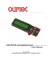
AVR-USB-STK development board
Users Manual
All boards produced by Olimex are ROHS compliant
Rev.A, July 2008
Copyright(c) 2008, OLIMEX Ltd, All rights reserved
INTRODUCTION:
AVR-USB-STK is easy to use development board for the new AT90USB162
microcontroller. With AT90USB162 is very easy to develop USB
functionality to your next device, as Atmel provide free open source HID
(mouse, keyboard) and CDC (USB-to-RS232) code and on top of this
AT90USB162 cost is same as ATMega16, so what you are waiting for?
AVR-USB-STK board allow all USB features of AT90USB162 to be explored.
The board have USB connector, Joystick, RS232, SD-MMC card, Audio
output, ICSP connector and extension connector. All AT90USB162 come
from Atmel pre-programmed with bootloader which allow code to be
programmed inside the chip without any external programmer, just
download the FLIP software from Atmel web site and load your HEX code
inside AT90USB162. To enter the bootloader mode you should press and
hold HWB button, then press and release RST button. If you prefer to use
ICSP programmer note that only AVR-DRAGON and AVR-ISP-MK2 is
supporting AT90USB162 as these are pretty new devices, probably AVR
Dude will add support later, but for the moment you can't use AVR-PG1 or
AVR-PG2 for ICSP programming, another bad news is that AT90USB162
supports only debug Wire not JTAG so to debug it you should have the
expensive AT-JTAGICE-MK2 or AVR-DRAGON.
BOARD FEATURES:
-
AT90USB162 microcontroller with 16KB Flash, 512B RAM, 512B
EEPROM
ICSP 5x2 pin connector for in-circuit programming with AVR-ISP-MK2
(you generally don't need to use ICSP as you can program via USB)
Debug Wire could be performed by 3 wires connected to ICSP (ATJTAGICE-MK2 have such lose wire connector which to be used, you
need VCC, GND, RST signals only)
USB 2.0 Full speed connector
RS232 driver and connector
SD-MMC card connector
Audio out 3.5 mm jack connector
Extension connector with AVR port signals
Status LED
Joystick
User button HWB (can be used to enter bootloader mode after reset)
Reset button RST
Takes power from USB no need for external adapter
External power supply and voltage regulator if USB can't provide
enough power
Quartz crystal oscillator circuit 8Mhz
Extension pin headers for each uC pin
Four mounting holes 3.3 mm (0.13")
Grid 100 mils
GND bus
Vcc bus
FR-4, 1.5 mm (0,062"), green soldermask, white silkscreen component
print
Dimensions 77x72 mm (3x2.8")
ELECTROSTATIC WARNING:
The AVR-USB-STK board is shipped in protective anti-static packaging. The
board must not be subject to high electrostatic potentials. General practice
for working with static sensitive devices should be applied when working
with this board.
BOARD USE REQUIREMENTS:
Cables:
1.8 meter USB A-B cable. RS232 female/male DB9 cable for
connecting to PC RS232 port
Hardware: AVR-DRAGON, AVR-JTAGICEMK2 or compatible tools
Software: AVR Studio + WinAVR free development IDE and C compiler
PROCESSOR FEATURES:
AVR-USB-STK uses Atmel 8-bit AVR CPU AT90USB162 with these features:
- High Performance, Low Power AVR® 8-Bit Microcontroller
- Advanced RISC Architecture
- 125 Powerful Instructions – Most Single Clock Cycle Execution
- 32 x 8 General Purpose Working Registers
- Fully Static Operation
- Up to 16 MIPS Throughput at 16 MHz
- Non-volatile Program and Data Memories
- 8K / 16K Bytes of In-System Self-Programmable Flash
- Endurance: 10,000 Write/Erase Cycles
- Optional Boot Code Section with Independent Lock Bits
- USB boot-loader programmed by default in the factory
- In-System Programming by on-chip Boot Program hardware-activated
after reset
- True Read-While-Write Operation
- 512 Bytes EEPROM
- Endurance: 100,000 Write/Erase Cycles
- 512 Bytes Internal SRAM
- Programming Lock for Software Security
- USB 2.0 Full-speed Device Module with Interrupt on Transfer
Completion
- Complies fully with Universal Serial Bus Specification REV 2.0
- 48 MHz PLL for Full-speed Bus Operation : data transfer rates at 12
Mbit/s
- Fully independant 176 bytes USB DPRAM for endpoint memory
allocation
- Endpoint 0 for Control Transfers: from 8 up to 64-bytes
- 4 Programmable Endpoints:
- IN or Out Directions
- Bulk, Interrupt and IsochronousTransfers
- Programmable maximum packet size from 8 to 64 bytes
- Programmable single or double buffer
- Suspend/Resume Interrupts
- Microcontroller reset on USB Bus Reset without detach
- USB Bus Disconnection on Microcontroller Request
- USB pad multiplexed with PS/2 peripheral for single cable capability
- PS/2 compliant pad
- One 8-bit Timer/Counters with Separate Prescaler and Compare Mode
(two 8-bit PWM channels)
-
One 16-bit Timer/Counter with Separate Prescaler, Compare and
Capture Mode (three 8-bit PWM channels)
USART with SPI master only mode and hardware flow control
(RTS/CTS)
Master/Slave SPI Serial Interface
Programmable Watchdog Timer with Separate On-chip Oscillator
On-chip Analog Comparator
Interrupt and Wake-up on Pin Change
On Chip Debug Interface (debugWIRE)
Power-On Reset and Programmable Brown-out Detection
Internal Calibrated Oscillator
External and Internal Interrupt Sources
Five Sleep Modes: Idle, Power-save, Power-down, Standby, and
Extended Standby
Operating Voltages – 2.7V – 5.5V
Operating temperature - Industrial (-40°C to +85°C)
BLOCK DIAGRAM:
MEMORY MAP:
SCHEMATIC:
BOARD LAYOUT:
POWER SUPPLY CIRCUIT:
AVR-USB-STK can be powered from the USB port or from external power
supply. The polarity of the external power supply doesn't matter as there is
diode bridge at the front stage, this making possible AVR-USB-STK to be
powered with AC or DC power adapters. The input voltage should be in the
range of 7-12VDC or 6-9VAC. The board power consumption is about 15
mA.
RESET CIRCUIT:
AVR-USB-STK reset circuit consist of R4 pullup, RST button and R9
current limiting resistor. When RST button is pressed logical 0 is fed to the
AT90USB162 reset input. As the reset port may be configured by the
software as GPIO and output the current limiting resistor R9 is connected
between the RST button and the microcontroller.
CLOCK CIRCUIT:
8MHz quartz crystal is connected to AT90USB162 pin 1 (XTAL1) and pin 2
((PC0)/XTAL2). Internal PLL generates the 48Mhz necessary for the USB.
INPUT/OUTPUT:
Reset button with name RST.
Button with name HWB, connected to AT90USB162 pin 13 ((#CTS/#HWB/
TD/INT7)/PD7) which, if pressed, could activate the USB Bootloader after
reset or could be used as user button.
Joystick with name JOYSTICK_MT5_F with four used positions (up,
down, right, left).
Power LED (red) with name PWR.
User status LED (red) with name STAT.
JUMPER DESCRIPTION:
HP_SB_E
When the jumper is closed, it enables AT90USB162 to control
standby function of the audio amplifier U3 (TS4871). When the
jumper is open, U3 enter standby mode.
Default state is closed.
the
CONNECTOR DESCRIPTIONS:
ICSP:
Pin # Signal Name Pin #
Signal Name
1
MOSI
2
VCC (+3.3V)
3
NC
4
GND
5
RST
6
GND
7
SCLK
8
GND
9
MISO
10
GND
MOSI I/O
Master Out Slave In. SPI data transfer signal. It is either input or output
depending on whether the MCU is master or slave.
SCLK I/O
Serial (Synchronization) Clock. This is the synchronization signal. It could
be either input (MCU – slave) or output (MCU – master).
MISO I/O
Master In Slave Out. SPI data transfer signal. It is either input or output
depending on whether the MCU is master or slave.
EXT:
Pin # Signal Name Pin #
3.3V
Signal Name
GND
VIN
EXT_PWR
PB0
B5(SELECT)
PB1
SCLK
PB2
MOSI
PB3
MISO
PB4
B1(LEFT)
PB5
B2(UP)
PB6
B3(RIGHT)
PB7
B4(DOWN)
PC1
RST
PC2
CS_SD/MMC
PC4
USB_P
PC5
PWM_OUT
PC6
STNBY
PC7
INT4/ICP1
PD1
CP
PD0
+5V_USB +5V
(OC.OB/INT0)
PD2
RXD1
PD3
TXD1
PD4
(INT5)
PD5
WP
PD6
#RTS
PD7
#CTS/PD7
VIN
Input Voltage In. You could apply external voltage at this pin.
MOSI I/O
Master Out Slave In. SPI data transfer signal. It is either input or output
depending on whether the MCU is master or slave.
MISO I/O
Master In Slave Out. SPI data transfer signal. It is either input or output
depending on whether the MCU is master or slave.
SCLK I/O
Serial (Synchronization) Clock. This is the synchronization signal. It could
be either input (MCU – slave) or output (MCU – master).
USB_P Input USB Power. The board could take power supply over the USB.
PWM_OUT Output PWM Output. This signal is passed to the headphones amplifier.
STNBYOutputStand-by. This signal controls the standby mode of the audio amplifier.
CP
Input Card Present. This signal is part of the SD/MMC interface.
RXD1 Input Receive Data. This is the asynchronous data input for the RS232 interface.
TXD1 OutputTransmit Data. This is the asynchronous data output for the RS232
interface.
WP
Input Write Protection. This signal is part of the SD/MMC interface.
#RTS OutputRequest To Send. This signal is part of the RS232 interface.
#CTS Input Clear To Send. This signal is part of the RS232 interface.
RS232
Pin # Signal Name Pin #
Signal Name
1
NC
6
to pin 4
2
TXDOUT
7
RS-CTS
3
RXDIN
8
RS-RTS
4
to pin 6
9
GND
5
GND
TXDOUT Output Transmit Data. This is the asynchronous data output for the RS232
interface.
RXDOUT InputReceive Data. This is the asynchronous data input for the RS232 interface.
#RTS OutputRequest To Send. This signal is part of the RS232 interface.
#CTS Input Clear To Send. This signal is part of the RS232 interface.
SD-MMC
Pin #
Signal Name
Pin #
Signal Name
1
CS_SD/MMC
9
Pull-up to 3.3V
2
MOSI
10
WP
3
GND
11
Not Connected
4
VDD
12
Not Connected
5
SCLK
13
CP
6
GND
14
Pull-down
7
MISO
15
Pull-down
8
Pull-up to 3.3V
CS_SD/MMC Output Chip Select SD/MMC. This signal enables and disables the SD/MMC
connector.
MOSI
Output Master Out Slave In. As the access to the memory is via SPI
interface, this is data
output from the MCU (which is master) and input for
the memory card (which is
slave).
WP
Input Write Protection. This signal is part of the SD/MMC interface.
SCLK
Output Serial (Synchronization) Clock. This is the synchronization
clock for the data
transfer.
CP
Input Card Present. This signal is part of the SD/MMC interface.
MISO
Input Master In Slave Out. As the access to the memory card is via SPI
interface, this is
data input for the MCU(which is master) and data
output from the memory card
(which is slave).
USB
Pin #
Signal Name
1
+5V
2
D–
3
D+
4
GND
D- and D+ both form differential input or output depending on the direction
of the data flow.
PWR_JACK
Pin #
Signal Name
1
9VDC/6VAC
2
GND
Audio Out:
MECHANICAL DIMENSIONS:
All measurements are in inches.
ORDER CODE:
AVR-USB-STK – assembled and tested (no kit, no soldering required)
How to order?
You can order to us directly or by any of our distributors.
Check our web www.olimex.com/dev for more info.
Revision history:
REV.A
- created July 2008
Disclaimer:
© 2008 Olimex Ltd. All rights reserved. Olimex®, logo and combinations thereof, are
registered trademarks of Olimex Ltd. Other terms and product names may be trademarks of
others.
The information in this document is provided in connection with Olimex products. No
license, express or implied or otherwise, to any intellectual property right is granted by this
document or in connection with the sale of Olimex products.
Neither the whole nor any part of the information contained in or the product described in
this document may be adapted or reproduced in any material from except with the prior
written permission of the copyright holder.
The product described in this document is subject to continuous development and
improvements. All particulars of the product and its use contained in this document are
given by OLIMEX in good faith. However all warranties implied or expressed including but
not limited to implied warranties of merchantability or fitness for purpose are excluded.
This document is intended only to assist the reader in the use of the product. OLIMEX Ltd.
shall not be liable for any loss or damage arising from the use of any information in this
document or any error or omission in such information or any incorrect use of the product.