1
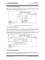
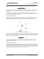
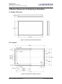
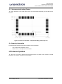
Application Note
Tag Design with swarm bee LE
Version: AN0504 Author: Nanotron Technologies
Tag Design
with swarm
bee LE
AN0504
NA-14-0267-0005-1.0
Application Note
Tag Design with swarm bee LE
Version: AN0504 Author: Nanotron Technologies
Document Information
Document Title:
Tag Design with swarm bee LE
Document Version:
AN0504
Current Date:
2014-09-29
Print Date:
2014-09-29
Document ID:
NA-14-0267-0005-1.0
Document Author:
Nanotron Technologies
Disclaimer
Nanotron Technologies GmbH believes the information contained
herein is correct and accurate at the time of release. Nanotron
Technologies GmbH reserves the right to make changes without
further notice to the product to improve reliability, function or
design. Nanotron Technologies GmbH does not assume any
liability or responsibility arising out of this product, as well as any
application or circuits described herein, neither does it convey any
license under its patent rights.
As far as possible, significant changes to product specifications and
functionality will be provided in product specific Errata sheets, or in
new versions of this document. Customers are encouraged to
check the Nanotron website for the most recent updates on
products.
Trademarks
All trademarks, registered trademarks, and product names are the
sole property of their respective owners.
This document and the information contained herein is the subject
of copyright and intellectual property rights under international
convention. All rights reserved. No part of this document may be
reproduced, stored in a retrieval system, or transmitted in any form
by any means, electronic, mechanical or optical, in whole or in part,
without the prior written permission of Nanotron Technologies
GmbH.
Copyright © 2009 Nanotron Technologies GmbH.
Page 2 Doc ID NA-14-0267-0005-1.0
© 2014 All Rights Reserved
Application Note
Tag Design with swarm bee LE
Version: AN0504 Author: Nanotron Technologies
Contents
1. Introduction ............................................................................................................................................... 4
2. Tag Building Blocks .................................................................................................................................. 4
2.1. Antenna .............................................................................................................................................. 4
2.1.1. Chip Antenna ............................................................................................................................... 4
2.1.2. U.FL Standard Connector ............................................................................................................ 5
2.2. Transceiver......................................................................................................................................... 6
2.3. Optional Host...................................................................................................................................... 6
2.3.1. Basic Tag Functionality ................................................................................................................ 6
2.3.2. Extended Tag Functionality with a Host Microcontroller .............................................................. 6
2.4. Power Supply ..................................................................................................................................... 6
2.4.1. Logic Levels ................................................................................................................................. 6
2.5. Housing .............................................................................................................................................. 6
3. Utilizing swarm bee as a Tag .................................................................................................................... 6
3.1. Tag without Host Controller ................................................................................................................ 7
3.2. Tag with Host Controller ..................................................................................................................... 7
4. Power Management .................................................................................................................................. 7
4.1. Power-saving Modes .......................................................................................................................... 8
4.2. Calculating Power Dissipation ............................................................................................................ 8
4.3. Battery Lifetime .................................................................................................................................. 8
4.3.1. Collaborative Location (Ranging) ................................................................................................. 8
4.3.2. Fixed Location (TDOA) ................................................................................................................ 9
4.3.3. Combined Location Modes .......................................................................................................... 9
5. Module Dimension & Soldering Information ............................................................................................ 10
5.1. Module Dimension ............................................................................................................................ 10
5.2. Footprint ........................................................................................................................................... 10
5.3. Recommended Landing Pattern ....................................................................................................... 11
5.4. Soldering Information ....................................................................................................................... 11
6. Firmware Updates................................................................................................................................... 11
7. References.............................................................................................................................................. 12
© 2014 All Rights Reserved
Doc ID: NA-14-0267-0005-1.0 Page 3
Application Note
Tag Design with swarm bee LE
Version: AN0504 Author: Nanotron Technologies
1. Introduction
The swarm bee CSS radio module is a fully integrated wireless node. The module works both in
applications with collaborative location technology based on TOF (ranging) and fixed location technology
based on TDOA (time difference of arrival) and supports concurrent communication. This application note
describes the necessary steps to create tag designs utilizing the swarm bee LE module. It explains how to
utilize nanotron’s new swarm bee radio module to build smart tags with host controller and basic tags
without host controller. Circuit diagrams for both architectures are shown and could easily be replicated by
the user for rapid prototyping and quick time to market. Design recommendations are provided with
regards to antenna design, power management and mechanical design. Calculation examples help to
estimate battery life depending on application specific parameters like the location blink rate.
2. Tag Building Blocks
A swarm bee tag, as shown in Figure 2-1, mainly comprises the following blocks: antenna, transceiver,
optional host, power supply and housing.
swar
Optio
Ho
usi
ng
Power Supply
Figure 2-1 general building blocks of a swarm bee tag
2.1. Antenna
The swarm bee RF interface is a standard 50 Ohm RF-port which requires a 50 Ohm load for optimal RF
performance. It is possible to connect antennas via RF connectors like U.FL as well as printed PCB
antennas or chip antennas. The RF port is DC-decoupled.
2.1.1. Chip Antenna
A chip antenna needs to create a 50 Ohm load impedance. The matching networks can be usually found
in the data sheet of the chip antenna.
The design of the matching network mostly depends on the used carrier material of the PCB. It is
recommended to measure the related parameters in a RF-Lab to get an optimized design result. The
leading line to the antenna must have a 50 Ohm impedance.
There are a lot of manufacturers who can provide 2.4 GHz chip antenna, for example Antenova, Murata,
Taiyo Yuden, TDK, Yageo, Johanson, etc. Figure 2-2 shows a chip antenna from Johanson, type
2450AT43A100.
Page 4 Doc ID NA-14-0267-0005-1.0
© 2014 All Rights Reserved
Application Note
Tag Design with swarm bee LE
Version: AN0504 Author: Nanotron Technologies
Figure 2-2 antenna on a two-layer PCB
2.1.2. U.FL Standard Connector
Alternatively, an external antenna can be chosen for the swarm bee tag. It can bee connected to swarm
bee LE module through a 2.4 GHz RF-connector on the carrier board of the module. A widely used
connector of this kind is a U.FL-R-SMT connector, for example from the company Hirose, see Figure 2-3.
A proper RF-cable must be chosen to connect an antenna via U.FL connector.
Figure 2-3 U.FL-R-SMT connector for an external antenna
Pay attention to the following during the use of U.FL connectors:
-
The leading line from swarm bee LE module to U.FL connector must be as short as possible;
The leading line must have a 50 Ohm impedance;
The leading line must be embedded in GROUND;
No signal lines shall run in the PCB layer directly under the connector;
Adjacent ground planes in different PCB layers must be connected with as many vias as possible;
The ground frames surrounding the U.FL connector must be at least 5 mm away from the via
lines. The area of the layer directly under the U.FL connector must be designed as GROUND.
Figure 2-4 shows a U.FL connector with a curved leading line on a PCB.
Figure 2-4 U.FL connector on a PCB
© 2014 All Rights Reserved
Doc ID: NA-14-0267-0005-1.0 Page 5
Application Note
Tag Design with swarm bee LE
Version: AN0504 Author: Nanotron Technologies
2.2. Transceiver
In each swarm bee LE module, the key block of a swarm bee tag, there is a nanoLOC TRX transceiver
chip based on nanotron’s CSS (Chirp Spread Spectrum) technology. The nanoLOC integrated circuit
operates in the freely accessible 2.4 GHz ISM band.
Please refer to [1] for more information about the nanoLOC transceiver.
2.3. Optional Host
The swarm bee LE module supports a number of basic tag functionalities like periodical transmission of a
location broadcast. To utilize the basic tag functionality the module can be operated in stand-alone mode,
as shown in figure 3-1. If extended tag functionality is required, swarm bee LE should be used in
conjunction with a host microcontroller. Using a microcontroller also provides more flexibilty to configuring
the tag for different modes of operation. In most cases, the performance of a small low-power 8-bit
controller will be sufficient. The configuration as a tag with or without controller is done by pulling pin 4 of
swarm bee LE to ground or leaving it open (open is equal to pushing pin 4 to high) respectively. Please
refer to figure 3-2.
2.3.1. Basic Tag Functionality
Tags based on a stand-alone swarm bee LE module are suitable for collaborative and fixed location
applications. They are able to transmit location broadcasts and respond to ranging requests. Most recent
readings from the on-board MEMs and temeprature sensors are transmitted in each of the location
broadcasts as payload. Please refer to [3] for a complete list of pre-set parameters. The tag can be
powered down periodically by pulling MOD_EN low (figure 3-1).
2.3.2. Extended Tag Functionality with a Host Microcontroller
Together with a host microcontroller the swarm bee LE module offers several location, communication and
configuration options beyond the basic tag functionality. In this configuration a tag user interface – for
instance a buzzer and/or push buttons – can be implemented.
2.4. Power Supply
swarm bee LE supports the supply voltage range between 3.0 V and 5.5 V. Direct supply from primary or
rechargeable batteries is possible as well as external supply from a USB source.
2.4.1. Logic Levels
Regardless of the power supply voltages of swarm bee LE and host, the digital signal levels from host and
module are subject to the following restrictions (relative to the swarm bee LE module):
-
-
VIL (input voltage low):
VIH (input voltage high):
VOL (output voltage low):
VOH (output voltage high):
FT Input (five- volt tolerant input):
max. 0.7 V
max. 2.8 V
max. 0.45 V
min. 2.15 V
max. 5.5 V
For pin configuration and supply voltage range of swarm bee LE please refere to [2]. If host and module
work from different supplies level shifters might be necessary.
2.5. Housing
The swarm bee LE module together with an optional host is usually mounted onto a carrier board, which
(including or excluding power supply) is then put into a housing to build a tag. Operating conditions such
as temperature, humidity etc. must be taken into consideration to choose the right material of the housing.
3. Utilizing swarm bee as a Tag
According to requirements of an application, a swarm bee tag can be designed as a tag without host
controller or as a smart tag with an external host controller.
Page 6 Doc ID NA-14-0267-0005-1.0
© 2014 All Rights Reserved
Application Note
Tag Design with swarm bee LE
Version: AN0504 Author: Nanotron Technologies
3.1. Tag without Host Controller
Figure 3-1 shows a possible configuration of swarm bee tag for stand-alone operation with a (chip)
antenna. When an external host is connected, i.e. for debugging purpose, the same signal level
restrictions are valid as for Tag configuration with internal host.
Figure 3-1 autonomous tag without host controller
3.2. Tag with Host Controller
Figure 3-2 shows a possible configuration of swarm bee as a tag with host. The power supply voltage
range for swarm bee must be within 3 V … 5.5 V. The host may have the same or a different power supply
voltage. Important are the correct levels of digital signals between swarm bee and the host.
By pulling pin 6 (MOD_EN) to logical LOW, the swarm bee LE module can be completely disabled. In this
case, the module draw a current of less than 1uA. The swarm bee LE module can be enabled by leaving
pin 6 open or setting it to HIGH with a level from 1.5 V to VDD of swarm bee.
Figure 3-2 tag with host controller
4. Power Management
The swarm bee LE module could go to sleep and only wake up periodically for short periods of time in
order to save battery power. The underlying power management concept enables cooperation between
the radios of a larger swarm even if they sleep most of the time.
© 2014 All Rights Reserved
Doc ID: NA-14-0267-0005-1.0 Page 7
Application Note
Tag Design with swarm bee LE
Version: AN0504 Author: Nanotron Technologies
4.1. Power-saving Modes
Sleep modes or power-saving modes are specified in swarm API by the parameter TYPE in command
group “SPSA (SetPowerSavingMode)”.
TYPE = 0 Power saving off, device is continuously receiving;
TYPE = 1 Power saving on, device makes full use of power saving features, receiver not
continuously active;
TYPE = 2 Power saving on, wake up on interrupt.
According to requirements of the application, the user can choose proper power-saving modes for the tag
and configure it through swarm API commands. For a detailed description of the commands, please refer
to [3].
4.2. Calculating Power Dissipation
Power dissipation depends on the tag design, the use of power saving modes, the location update rate
and the location method adopted. Power dissipation varies for different application scenarios.
4.3. Battery Lifetime
The battery lifetime of a stand-alone tag can be calculated when power dissipation is known and the
battery capacity is given. In the following a sample calculation is shown for typical location sequences.
4.3.1. Collaborative Location (Ranging)
swarm bee tags can be used for collaborative location (shown in figure 4-1) where one moving tag ranges
with one or more other moving or fixed tags in its neighbourhood. Local anchors which have received
ranging results forward them to the location server which calculates the accurate location of the tag.
Figure 4-1 collaborative location of swarm bee tags
When a swarm bee tag only ranges to one other tag, the energy consumption for a ranging cycle has been
measured as about 1200 µAs, when the board is working in in 80MHz. If the ranging interval is 10 s, the
battery capacity 1200 mAh and the battery efficiency 90%, the approximate battery lifetime T1 can be
calculated as follows:
T1 =
1200 𝑚𝐴ℎ∗ 90 %
1200 µ𝐴𝑠 /10 𝑠
= 9000 h
When a swarm bee tag ranges to more than one tags, the energy consumption for a ranging cycle would
be increased by about 300 µAs per tag. If the other paramters are not changed, the approximate battery
lifetime T2 for ranging to two tags can be calculated as follows:
T2 =
Page 8 Doc ID NA-14-0267-0005-1.0
1200 𝑚𝐴ℎ∗ 90 %
(1200+300) µ𝐴𝑠 /10 𝑠
= 7200 h
© 2014 All Rights Reserved
Application Note
Tag Design with swarm bee LE
Version: AN0504 Author: Nanotron Technologies
Similarly, the approximate battery lifetime T3 for ranging to three tags can be calculated as follows:
T3 =
1200 𝑚𝐴ℎ∗ 90 %
(1200+300∗2) µ𝐴𝑠 /10 𝑠
= 6000 h
Ranging with just one tag provides proximity information only, ranging values from two tags can be used to
determine lateral location information and ranging with three reference tags allows to calculate a 2D
location value.
Note: To simplify the approximate calculation, the power down dissipation has been neglected. For an
accurate calculation of the battery lifetime, this parameter must be considered. Specifically for long ranging
intervalls this component might even dominate.
4.3.2. Fixed Location (TDOA)
swarm bee tags can be used for fixed location as well, see figure 4-2. During fixed location, a moving tag
sends out its node ID blink regularly. Anchors on fixed points receive the blinks and forward them to the
location server which calculates the location of the tag based on TDOA (time difference of arrival).
Figure 4-2 fixed location of a swarm bee tag
For this application the power consumption of a tag mostly depends on the blink interval and it is much
lower than in collaborative location. The measured value for each blink is about 900 µAs. If the blink
interval is 1 s, the battery capacity 1200 mAh and the battery efficiency 90%, the approximate battery
lifetime T4 can be calculated as follows:
T4 =
1200 𝑚𝐴ℎ∗ 90 %
900 µ𝐴𝑠 /1 𝑠
= 1200 h
Note: To simplify the approximate calculation, the power down dissipation has been neglected. For an
accurate calculation of the battery lifetime, this parameter must be considered. It dominates for long
phases of sleep between blinks.
4.3.3. Combined Location Modes
Depending on requirements of an application, swarm bee tags may be used for combined location modes,
i.e. in areas where relative location information is needed between radio nodes, a tag must range with
other tags in order to avoid collisions or dangers. In other areas, a tag may just need to send its own node
ID blink so that the server can detect the position of this tag. In this case, the battery lifetime of a tag can
be calculated combining parameters for both collaborative and fixed location.
© 2014 All Rights Reserved
Doc ID: NA-14-0267-0005-1.0 Page 9
Application Note
Tag Design with swarm bee LE
Version: AN0504 Author: Nanotron Technologies
5. Module Dimension & Soldering Information
5.1. Module Dimension
Figure 5-1 swarm bee LE module, dimensions
5.2. Footprint
Figure 5-2 swarm bee LE module, footprint
Page 10 Doc ID NA-14-0267-0005-1.0
© 2014 All Rights Reserved
Application Note
Tag Design with swarm bee LE
Version: AN0504 Author: Nanotron Technologies
5.3. Recommended Landing Pattern
The same dimensions for the solder paste screen are recommended, depending on the solder screen
thickness.
Figure 5-3 swarm bee LE module – footprint and landing pattern (top view)
5.4. Soldering Information
For lead-free reflow soldering, the follows conditions are recommended:
-
-
max. Solder Peak Temperature: 200°C
Solder Paste: for example ALPHA® CVP-520
6. Firmware Updates
The swarm bee LE module is delivered with the latest firmware. An update of the firmware is possible
through the host interface, see [4] for more information.
© 2014 All Rights Reserved
Doc ID: NA-14-0267-0005-1.0 Page 11
Application Note
Tag Design with swarm bee LE
Version: AN0504 Author: Nanotron Technologies
7. References
[1] nanoLOC Data Sheet, V2.01 as of 23.04.2008, Doc ID: NA-06-0230-0388-2.01
[2] swarm bee Data Sheet, V1.0 (Preliminary) as of 27.02.2014 , Doc ID: NA-14-0267-0002-1.0
[3] swarm API, V2.02 as of 18.03.2014, Doc ID: NA-13-0267-0003-2.02
[4] swarm bee Firmware Update User Guide, V1.0 as of 01.07.2014, Doc ID: NA-14-0267-0011-1.0
Page 12 Doc ID NA-14-0267-0005-1.0
© 2014 All Rights Reserved
Application Note
Tag Design with swarm bee LE
Version: AN0504 Author: Nanotron Technologies
End of Document
© 2014 All Rights Reserved
Doc ID: NA-14-0267-0005-1.0 Page 13
Application Note
Tag Design with swarm bee LE
Version: AN0504 Author: Nanotron Technologies
Document History
Date
Authors
30.09.2014
Nanotron
Technologies GmbH
Page 14 Doc ID NA-14-0267-0005-1.0
Versi
on
1.0
Description
Application note on how to use swarm as a tag in a real
time location system
© 2014 All Rights Reserved
Application Note
Tag Design with swarm bee LE
Version: AN0504 Author: Nanotron Technologies
Life Support Policy
These products are not designed for use in life support
appliances, devices, or systems where malfunction of these
products can reasonably be expected to result in personal
injury. Nanotron Technologies GmbH customers using or
selling these products for use in such applications do so at
their own risk and agree to fully indemnify Nanotron
Technologies GmbH for any damages resulting from such
improper use or sale.
Electromagnetic Interference / Compatibility
Nearly every electronic device is susceptible to
electromagnetic interference (EMI) if inadequately shielded,
designed, or otherwise configured for electromagnetic
compatibility. To avoid electromagnetic interference and/or
compatibility conflicts, do not use this device in any facility
where posted notices instruct you to do so. In aircraft, use of
any radio frequency devices must be in accordance with
applicable regulations. Hospitals or health care facilities may
be using equipment that is sensitive to external RF energy.
With medical devices, maintain a minimum separation of 15
cm (6 inches) between pacemakers and wireless devices and
some wireless radios may interfere with some hearing aids. If
other personal medical devices are being used in the vicinity of
wireless devices, ensure that the device has been adequately
shielded from RF energy. In a domestic environment this
product may cause radio interference in which case the user
may be required to take adequate measures.
CAUTION - Electrostatic Sensitive Device! Precaution
should be used when handling the device in order to prevent
permanent damage.
FCC User Information
Statement according to FCC part 15.19:
This device complies with Part 15 of the FCC Rules. Operation
is subject to the following two conditions: (1) this device may
not cause harmful interference, and (2) this device must
accept any interference received, including interference that
may cause undesired operation.
Statement according to FCC part 15.21:
Modifications not expressly approved by this company could
void the user's authority to operate the equipment.
RF exposure:
The internal / external antennas used for this mobile
transmitter must provide a separation distance of at least 20
cm from all persons and must not be co-located or operating in
conjunction with any other antenna or transmitter.
Statement according to FCC part 15.105:
This equipment has been tested and found to comply with the
limits for a Class A and Class B digital device, pursuant to Part
15 of the FCC Rules. These limits are designed to provide
reasonable protection against harmful interference in a resi-
About Nanotron Technologies GmbH
Nanotron provides reliable loss protection
technology and solutions that are used to protect
people and animals. Energy efficient, batterypowered wireless nodes are the key building
blocks. These small devices create a Virtual
Safety Zone which protects tagged people and
animals. Robust wireless Chirp technology
underpins nanotron’s offering of chips, modules
and loss protection software for indoor and
outdoor environments world wide.
dential installation and against harmful interference when the
equipment is operated in a commercial environment.
This equipment generates, uses, and can radiate radio frequency energy and, if not installed and used in accordance
with the instructions as provided in the user manual, may
cause harmful interference to radio communications. However,
there is no guarantee that interference will not occur in a
particular installation. Operation of this equipment in a residential area is likely to cause harmful interference in which
case the user will be required to correct the interference at his
or her own expense.
If this equipment does cause harmful interference to radio or
television reception, which can be determined by turning the
equipment off and on, the user is encouraged to try to correct
the interference by one or more of the following measures: (1)
reorient or relocate the receiving antenna, (2) increase the
separation between the equipment and receiver, (3) connect
the equipment into an outlet on a circuit different from that to
the connected equipment, and (4) consult the dealer or an
experienced technician for help.
Headquartered in Berlin, Germany, Nanotron Technologies
GmbH was founded in 1991 and is an active member of IEEE.
Further Information
For more information about products from Nanotron
Technologies GmbH, contact a sales representative at the
following address:
Nanotron Technologies GmbH
Alt-Moabit 60
10555 Berlin, Germany
Phone: +49 30 399 954 – 0
Fax: +49 30 399 954 – 188
Email: [email protected]
Internet: www.nanotron.com