1
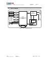
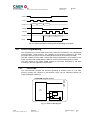
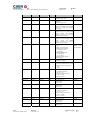
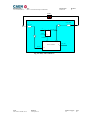
Document type:
User's Manual (MUT)
Title:
Mod. V1495 General Purpose VME Board
Revision date:
20/07/2010
Revision:
10
The sequence to be followed is:
Step 1: write 0x1 in the PDL_CONTROL register
Step2: update the dip switches value
B) updating of PDL1 delay via switch:
Step 1: write 0x5 in the PDL_CONTROL register
Step 2: update the dip switches value
C) updating of PDL0 delay via VMEbus:
Step 1: write 0x3 in the PDL_CONTROL register
Step2: write the delay value in the PDL_DATA register
D) updating of PDL1 delay via VMEbus:
Step 1: write 0x7 in the PDL_CONTROL register
Step2: write the delay value in the PDL_DATA register
GATE WIDTH (USING Delay Line Oscillators)
The GATEWIDTH register can be used to set the gate signal width on the G port (see
Delay Unit using DLOs, see § 5.5.6).
5.5.5.
Delay Unit using PDLs
The following diagram shows the implementation of the DELAY_UNIT using the one of
the two programmable delay lines (PDL) available on the boards.
PDLx
PDLx_IN
PDLx_OUT
MONOSTABLE
'1'
D
COINC
PULSE
GEN.
(360 ns
pulse)
Q
CLK
CLR
STARTDELAY
'1'
D
Q
STOPDELAY
PDL_PULSEOUT
CLK
CLR
STOPDELAY
Fig. 5.4: Delay Unit with PDLs
NPO:
00117/04:V1495.MUTx/10
Filename:
V1495_REV10
Number of pages:
40
Page:
33