1
ECEN 449: Microprocessor System Design
Department of Electrical and Computer Engineering
Texas A&M University
Prof. Peng Li
TA: Andrew Targhetta
(Lab exercises created by A. Targhetta / P. Gratz)
Laboratory Exercise #2
Using the Xilinx Platform Studio (XPS)
Objective
The purpose of lab this week is to familiarize you with XPS by developing a software based solution for
controlling the LEDs in a manner similar to that which was done last week in pure FPGA hardware. To
accomplish this goal, you will be guided through the process of creating a MicroBlaze processor system
using the XPS Base System Builder (BSB). You will then add General Purpose Input/Output (GPIO) capabilities to the microprocessor via Intellectual Property (IP) hardware blocks from Xilinx. Finally, you will
create software using the C programming language, which will run on the MicroBlaze processor inorder to
implement the appropriate LED functionality.
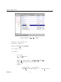
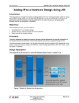
System Overview
The microprocessor system you will build in this lab is depicted in Figure 1. At the center of the diagram
is the MicroBlaze soft IP processor. Connected to it are two Local Memory Buses (LMBs), iLMB and
dLMB for instruction fetch and data access respectively. Each LMB has its own block RAM (BRAM)
controller which provides the interconnect logic between the MicroBlaze and BRAM (local memory). The
Processor Local Bus (PLB) connects the MicroBlaze (bus master) to peripherals (bus slaves) external to
the microprocessor. Typically included in the list of peripherals are the debugger module and a Universal
Asynchronous Receiver Transmitter (UART). The debugger allows XPS to interact with the MicroBlaze
1
2
Laboratory Exercise #2
processor after the FPGA has been programmed. This is useful for initializing regions of memory outside
of the FPGA and for general software debugging. The UART is used for RS232 communication, which
will be our primary method of communicating with the microprocessor for the next few labs. The GPIO
blocks provide the microprocessor with a means of controlling the LEDs and reading user input from the
DIP switches and push buttons.
PLB
JTAG
Debug
Block RAM
BRAM Cntlr
iLBM
UART
RS232
GPIO
LEDs
BRAM Cntlr
dLBM
MicroBlaze
Processor
Switches
GPIO
Push Buttons
Figure 1: MicroBlaze System Diagram
Procedure
1. Launch Platform Studio and run Base System Builder (BSB).
(a) Before beginning, create a directory in your home folder for today’s lab. Try to avoid spaces and
special characters in the directory name as they have the potential for causing problems during
2
ECEN 449
Laboratory Exercise #2
3
the system build process. You may use the ‘mkdir’ command in an open terminal to create a
directory.
(b) Next, type the following commands in the terminal window:
>source /homes/faculty/shared/ECEN449/settings.csh
>xps
The former will setup the environment for XPS and kermit, a serial console required for lab this
week.
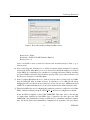
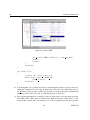
(c) Once XPS comes up, select ‘Base System Builder wizard’ in first prompt (Figure 2). Hit ‘OK’
to continue.
Figure 2: Begin Base System Builder
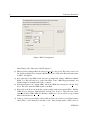
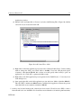
(d) In the next window (Figure 3), define the ‘Project file’ as “system.xmp” within your project
directory created in step 1(a).
(e) In the same window, check ‘Set Project Peripheral Repositories’ and hit ‘Browse’ to set
/homes/faculty/shared/ECEN449/EDK-XUPV5-LX110T-Pack/lib
as the project peripheral repositories for this lab. Hit ‘OK’ to proceed.
(f) At this point, the BSB welcome window appears. Select ‘I would like to create a new design’
and hit ‘Next’ to start BSB with a blank design.
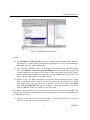
(g) The ‘Select Board’ window (Figure 4) will now come up. Set the following fields before continuing:
ECEN 449
3
4
Laboratory Exercise #2
Figure 3: Project file and Project Peripheral Repositories
Board vendor : Xilinx
Board name : XUPV5-LX110T Evaluation Platform
Board revision : A
Leave ‘I would like to create a system for a custom board’ unselected and press ‘Next’ to go to
the next screen.
(h) Now you should get the ‘Select Processor’ window. Accept the defaults in which ‘Use stepping’
is unselected and the ‘MicroBlaze’ processor is selected. Note that the PowerPC is not an option
for this FPGA. It is a hard IP processor included on some high-end Virtex-5 FPGAs and many
pre-Virtex-5 FPGAs such as the Virtex-II. Before pressing ‘Next’, please take a moment to read
the ‘Processor description’ for the MicroBlaze.
(i) In the ‘Configure MicroBlaze Processor’ window, leave the ‘Processor-Bus clock’ at 125Mhz,
keep the ‘Debug I/F’ field on default, and leave ‘Local memory’ set to 8 KB. We will end up
changing this later on in the lab; however the drop box here only goes up to 64KB and we need
128KB. Try to understand what the rest of the options mean but leave them as default as well.
(j) The next five BSB steps are for configuring the peripherals connected to our Processor Local Bus
(PLB). Uncheck everything except the ‘RS232 Uart 1’ and leave its configuration as default.
Notice the RS232 peripheral is called ‘XPS UARTLITE’. This name refers to the fact that
it is light-weight, requiring very little FPGA logic. Compared to the other option, the ‘XPS
UART16550’, the communication settings are hardcoded, i.e. determined at hardware synthesis
time. For this lab, hardcoded communication configurations are acceptable. Also note that we
4
ECEN 449
Laboratory Exercise #2
5
Figure 4: Base System Builder - Select Board
are not using interrupts in this design.
(k) After specifying the peripherals connected to the PLB, the ‘Software Setup’ window (Figure 6)
will come up. Uncheck ‘Memory test’ and ‘Peripheral selftest’. These are test applications that
XPS will autogenerate for us. We have no intentions of using them so we will not clutter up our
project with them.
Note the first two fields in Figure 6. These point to the RS232 peripheral we specified previous
for STDIN and STDOUT. Essentially, STDIN and STDNOUT link printf and scanf to the serial
port on the XUP board. The third field specifies where the boot code should be placed on the
finished system. Upon reset, the microprocessor must know where to start executing code, and
this is that area of memory. In our simple system, the BRAMs are the only memories we have
(recall from the system diagram that the iLMB controller connects directly to the BRAM.
(l) Hit ‘Next’ to continue. The ‘System Created’ screen will provide you with a summary of the
system BSB will setup for you. Press ‘Generate’ to go forward with your design. Finally, click
‘Finish’ on the last prompt.
2. Once the BSB completes, we will have a blank system without the GPIO peripherals. The following
steps will now guide you through the process of adding a GPIO IP block to our microprocessor based
system and connecting that block to the LEDs on the XUP board.
(a) In the upper left hand corner of the XPS window, select the ‘IP Catalog’ tab. A list of IP
categories will be displayed. Expand the ‘General Purpose IO’ category and right click on ‘XPS
ECEN 449
5
6
Laboratory Exercise #2
Figure 5: RS232 Configuration
General Purpose IO’. Then select ‘Add IP’ (Figure 7).
(b) XPS responds by adding an IP block called ‘xps gpio 0’ to the project. This can be seen now in
the ‘System Assembly View’ under the ‘Bus Interfaces’ tab. Click on this IP module and rename
it ‘LEDs’. See Figure 8.
(c) Now, right click on the GPIO module and select ‘Configure IP’. Change ‘GPIO Data Channel
Width’ to 4. This will allow us to control four LEDs. Leave ‘GPIO Supports Interrupts’ and
‘Enable Channel 2’ unchecked. Hit ‘OK’ to continue.
(d) In the ‘Bus Interfaces’ tab, expand ‘LEDs’ and set the ‘SPLB’ bus connection to ‘mb plb’ (Figure 9). This will connect the GPIO module to the PLB.
(e) Next, click on the ‘Ports’ tab under the system assembly window and expand ‘LEDs’. Find the
‘GPIO IO’ port and select ‘Make External’ from the ‘Net’ drop box. This will create a 4-bit
external port called ‘LEDs GPIO IO’. Rename it ‘LEDs ext’ so we do not have to type as much
when we modify the ucf.
(f) At the top of the system assembly window with the ‘Ports’ tab selected, you will find a button
called ‘Filters’. Select that button and click on ‘All’. Then, navigate back to ‘LEDs’ and look
6
ECEN 449
Laboratory Exercise #2
7
Figure 6: Software Setup
for the ‘SPLB Clk’ port. Set the net connection to ‘sys clk s’.
(g) We are almost done adding a GPIO IP to our microprocessor system! Now we must specify an
address range on the bus for our LEDs module. To do this, select the ‘Addresses’ tab under the
system assembly window. Set the ‘size’ field of ‘LEDs’ to 64K and hit the ‘Generate Addresses’
button. This will adjust the address ranges for other IP blocks in our system. Ensure there are
no overlapping address.
(h) While under the ‘Addresses’ tab, change the sizes of both the dlmb cntlr and ilmb cntrl to 128K
and regenerate the hardware addresses. It turns out that 64K is not enough memory for our
system when using printf in your application code.
(i) The final step is to modify the ucf to specify the pin locations of LEDs ext. Click on the ‘Project’
tab in the upper left corner of the XPS window. Locate the ‘data/system.ucf’ file and double click
on it. In the editor window that appears, append the following code to the ucf:
NET
NET
NET
NET
"LEDs_ext<0>"
"LEDs_ext<1>"
"LEDs_ext<2>"
"LEDs_ext<3>"
LOC
LOC
LOC
LOC
=
=
=
=
"H18" ;
"L18" ;
"G15" ;
"AD26" ;
Does this code snippet look familiar? Be sure to save the ucf when you are done editing it.
3. After modifying the ucf, we must build our hardware system and generate the appropriate software
ECEN 449
7
8
Laboratory Exercise #2
Figure 7: Add XPS General Purpose IO
libraries.
(a) Select Hardware→Generate Netlist from the top menu of the XPS window. This will take a
few moments to complete as XPS synthesizes the various IP blocks in your system including the
MicroBlaze processor and the GPIO module.
(b) Once complete, you will see “Done!” in the output console at the bottom of the XPS window.
Next, select Software→Generate Libraries and BSPs from the top menu. This operation will
complete much faster than the previous operation. XPS will compile the necessary libraries
based on the hardware configurations found in the system assembly window. Just as before, you
will see “Done!” in the output console when complete.
(c) Before we start our software development, we should start the implementation phase as this
takes a considerable amount of time. So far, we have synthesized our hardware, but now XPS
must translate, map, and place and route our hardware. From the top menu, select Hardware→Generate Bitstream. This will also attempt to compile any application code and initialize the BRAMs. We have no application code at this point.
4. To complete our simple microprocessor system, we must develop the software to drive the LEDs. The
next few steps will guide you through the software development process using C programming and
the XPS development tools.
(a) Using you favorite editor, create a file called “lab2a.c”. Type the uncommented C code shown
below in your file and save it in your lab2 directory.
8
ECEN 449
Laboratory Exercise #2
9
Figure 8: Rename ‘xps gpio 0’ to ‘LEDs’
# i n c l u d e <x p a r a m e t e r s . h>
# i n c l u d e <x g p i o . h>
# d e f i n e WAIT VAL 0 x1000000
i n t delay ( void ) ;
i n t main ( )
{
i n t count ;
i n t count masked ;
XGpio l e d ;
X G p i o I n i t i a l i z e (& l e d , XPAR LEDS DEVICE ID ) ;
X G p i o S e t D a t a D i r e c t i o n (& l e d , 1 , 0 ) ;
count = 0;
while (1)
{
count masked = count & 0 xf ;
X G p i o D i s c r e t e W r i t e (& l e d , 1 , c o u n t m a s k e d ) ;
ECEN 449
9
10
Laboratory Exercise #2
Figure 9: Connect to PLB
x i l p r i n t f ( ” LEDs = 0 x%x \n \ r ” , c o u n t m a s k e d ) ;
delay ( ) ;
c o u n t ++;
}
return (0);
}
i n t delay ( void )
{
v o l a t i l e i n t delay count = 0;
w h i l e ( d e l a y c o u n t < WAIT VAL )
d e l a y c o u n t ++;
return (0);
}
(b) Look through the code you just wrote and try to understand what exactly is going on. Notice we
include the ”xparameters.h” and ”xgpio.h” header files. These files are located in the ‘microblaze 0/include/’ directory under you lab2 project directory. Open up these files and understand
what they provide. At the end of lab, you will find questions on these files.
(c) Once system implementation is complete, select the ‘Applications’ tab in the upper left corner
of the XPS window. Then, click on ‘Add Software Application Project’. Enter “lab2a” for the
‘Project Name’ and hit ‘OK’. You should now see a ‘lab2a’ application project show up in the
10
ECEN 449
Laboratory Exercise #2
11
Applications window.
(d) Expand ‘lab2a’ and right click on ‘Sources’ and select ‘Add Existing Files’ (Figure 10). Add the
source file we just created and click ‘OK’.
Figure 10: Add Source File to lab2a
(e) Right click on the lab2a application project and select ‘Generate Linker Script’. In the resulting
window, change the ‘Heap’ and ‘Stack’ fields to 0x4000. If we had other physical regions
of memory other than the BRAM, this is where we would specify where exactly to place our
application code. Click ‘OK’ to generate the linker script.
(f) Right click on the lab2a application project again and select ‘Build Project’. Correct any errors
in the build process.
(g) Once again right click on the lab2a application project and select ‘Mark to Initialize BRAMs’.
This tells XPS to initialize the BRAM memory with the lab2a application. Ensure the projects
other than lab2a are not marked to initialize in BRAM.
5. At this point, both the hardware and software have been created. We will now use XPS to create a
bitstream and load it onto the FPGA. You should have noticed that the code includes printf statements.
ECEN 449
11
12
Laboratory Exercise #2
The output of those statements are directed to the rs232 port, and we will use a serial console on the
CentOS machines to display them.
(a) In the top menu, select Device Configuration→Update Bitstream. This will combine the hardware bitstream created earlier with the BRAM initialization bitstream taken from the executable
and linkable format (elf) file. The result is an ‘download.bit’ file stored in the ‘implementation’
directory under your lab2 directory.
(b) Ensure the XUP board is turned on. To download the bitstream to the FPGA, select Device
Configuration→Download Bitstream from the top menu.
(c) If everything is correct, you should see the LEDs on the XUP board count as seen in the lab
before. Note that you do not have to hold the up or down buttons in for the LEDs to count.
(d) To see the output of the printf statements in our code, we must use ‘kermit’, a serial console
application on the CentOS machines. Open a terminal window and type the following:
>source /homes/faculty/shared/ECEN449/settings.csh
>kermit -l /dev/ttyS0
You should see the kermit prompt. In kermit, type the following:
C-Kermit>set speed 9600
C-Kermit>connect
If everything is correct, you will see text being printed to the serial console. Demostrate your
progress to the TA.
Deliverables
1. [4 points.] Demonstrate your work to the TA after downloading the bitstream for the design created
using the steps provided in the manual. Add comments to your C code and the modified portion of
the ucf file and include them in your lab write-up.
2. [12 points.] Add an 9-bit GPIO IP block to your system and connect the lower 4-bits to the DIP switchs
and the upper 5-bits to the push buttons on the XUP board. Then, develop software to implement the
following functionality:
When the North push button is pressed, the LEDs should count up. When the South
push button is pressed, the LEDs should count down. When the West push button is
pressed, the current count should be displayed on the LEDs. When the East push button is pressed, the status of the DIP switches should be displayed. The count should reset
when you push the center push button. The serial console should display the current action
and LEDs value.
Hints:
12
ECEN 449
Laboratory Exercise #2
13
• When configuring the additional GPIO, if you set the ‘Channel 1 is input only’ field to ‘TRUE’,
be sure you connect the input signals to the ‘GPIO in’ port.
• Skim through the user manual for the XUPV5 board to determine the pin assignments for additional signals. The user manual may be found on the course website.
• Do not forget to add the DIP switches and push buttons to your UCF before generating the
netlist.
• Your source code must detect a change on the push buttons and DIP switches and react accordingly. When a change is detected, print the current action and LEDs value to the terminal
window. Also, print to the terminal everytime the LEDs value changes.
3. [4 points.] Answer the following questions:
(a) In the first part of lab, we created a delay function by implementing a counter. The goal was to
update the LEDs approximately every second as we did in the previous lab. Compare the count
value in this lab to the count value you used as a delay in the previous lab. If they different,
explain why? Can you determine approximately how many clock cycles are required to execute
one iteration of the delay for-loop? If so, how many?
(b) Why is the count variable in our software delay declared as volatile?
(c) What does the while(1) expression in our code do?
(d) Compare and contrast this lab with the previous lab. Which implementation do you feel is easier?
What are the advantages and disadvantages associated with a purely software implementation
such as this when compared to a purely hardware implementation such as the previous lab?
ECEN 449
13