1
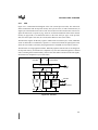
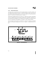
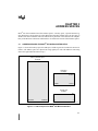
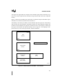
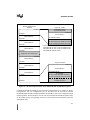
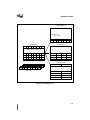
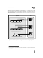
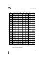
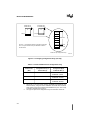
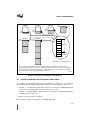
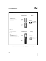
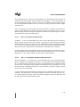
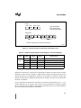
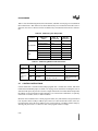
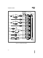
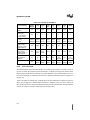
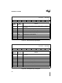
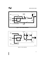
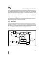
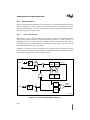
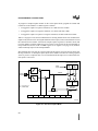
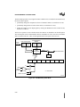
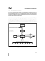
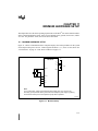
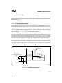
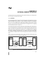
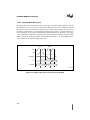
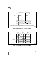
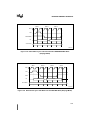
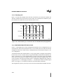
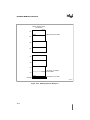
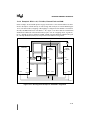
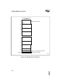
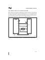
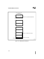
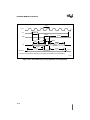
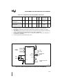
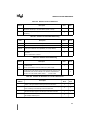
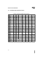
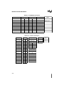
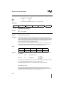
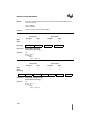
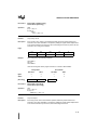
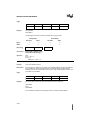
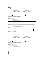
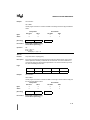
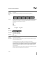
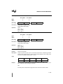
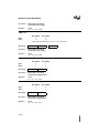
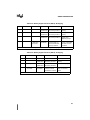
DEVICE CONFIGURATION
A key to the memory interface is the relationship between internal memory addresses and external memory addresses. While the 8XC251Sx has 24 internal address bits, the number of external
address lines is less than 24 (i.e., 16, 17, or 18 depending on the values of RD1:0). This means
that reads/writes to different internal memory addresses can access the same location in external
memory.
For example, if the 8XC251Sx is configured for 18 external address lines, a write to location
03:6000H and a write to location FF:6000H accesses the same 18-bit external address (1:6000H)
because A16 = 1 and A17 = 1 for both internal addresses. In other words, regions 00: and FC:
map into the same 64-Kbyte region in external memory.
In some situations, however, a multiple mapping from internal memory to external memory does
not preclude using more than one region. For example, for a device with on-chip ROM/
OTPROM/EPROM configured for 17 address bits and with EA# = 1, an access to FF:0000H–
FF:3FFFH (16 Kbytes) accesses the on-chip ROM/OTPROM/EPROM, while an access to
03:0000H–03:3FFFH is to external memory. In this case, you could execute code from these locations in region FF: and store data in the corresponding locations in region 03: without conflict.
See Figure 4-7 and “Example 3: RD1:0 = 01, 17-bit Bus, External RAM” on page 13-17.
4.6.2.1
RD1:0 = 00 (18 External Address Bits)
NOTE
The combination RD1:0 = 00 is invalid for the A-stepping 8XC251SB.
The selection RD1:0 = 00 provides 18 external address bits: A15:0 (ports P0 and P2), A16 (from
P3.7/RD#/A16), and A17 (from P1.7/CEX4/A17). Bits A16 and A17 can select four 64-Kbyte
regions of external memory for a total of 256 Kbytes (top half of Figure 4-7 on page 4-13). This
is the largest possible external memory space. Regions 00: and FC: (each having A17:16 = 00)
map into the same 64-Kbyte region in external memory. This duplication also occurs for regions
01: and FD:, 02: and FE:, and 03: and FF:. See “Example 1: RD1:0 = 00, 18-bit Bus, External
Flash and RAM” on page 13-13.
4.6.2.2
RD1:0 = 01 (17 External Address Bits)
The selection RD1:0 = 01 provides 17 external address bits: A15:0 (ports P0 and P2) and A16
(from P3.7/RD#/A16). Bit A16 can select two 64-Kbyte regions of external memory for a total
of 128 Kbytes (bottom half of Figure 4-7 on page 4-13). Regions 00:, 02:, FC:, and FE: (each having A16 = 0) map into the same 64-Kbyte region in external memory. This duplication also occurs
for regions 01:, 03:, FD:, and FF:.
4-12