1
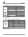
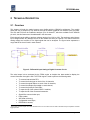
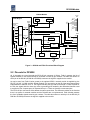
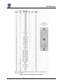
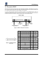
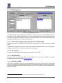
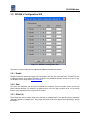
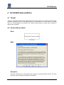
Current Sensor Module
OP6228
(Part # 519-XXXX)
OP6228 Module
Table of contents
1
INTRODUCTION .................................................................................................................................................................. 5
1.1
1.2
1.3
1.4
1.5
1.6
2
TECHNICAL DESCRIPTION.............................................................................................................................................. 8
2.1
2.2
2.3
2.4
2.5
3
SCOPE ................................................................................................................................................................................ 5
OP6228 MODULE .............................................................................................................................................................. 5
OP6228 SPECIFICATIONS WITHOUT OPTIONAL OP5511 MODULE ........................................................................................ 6
OP6228 SPECIFICATIONS WITH OPTIONAL OP5511 MODULE ............................................................................................... 6
REFERENCE DOCUMENTS ................................................................................................................................................... 7
DEFINITIONS ...................................................................................................................................................................... 7
OVERVIEW ......................................................................................................................................................................... 8
PIN-OUTS FOR OP6228 ....................................................................................................................................................... 9
PIN-OUTS FOR OP5511 ..................................................................................................................................................... 12
ID VALUES FOR THE OP5511 PROBE ................................................................................................................................. 13
CHANNEL TEST OUTPUT .................................................................................................................................................... 13
GRAPHICAL USER INTERFACE (GUI) ......................................................................................................................... 15
3.1
OP6228’S TESTDRIVE GUI.............................................................................................................................................. 15
3.1.1
File Management .................................................................................................................................................... 16
3.1.1.1
Enable Data Logging checkbox and Save Current Data button....................................................................... 16
3.1.1.2
File progress.................................................................................................................................................... 16
3.1.1.3
Base File Name ............................................................................................................................................... 16
3.1.1.4
Max File Size (MB) ........................................................................................................................................ 16
3.1.1.5
Max File Index and Reset button..................................................................................................................... 17
3.1.1.6
Auto Increment ............................................................................................................................................... 17
3.1.1.7
Current File Index ........................................................................................................................................... 17
3.1.1.8
File folder........................................................................................................................................................ 17
3.1.1.9
List of files on Target with the Delete, Download, and Abort buttons ............................................................ 17
3.1.1.10
List of files on Host with the Delete and Display buttons and the Rename method........................................ 17
3.1.2
System Information and Trigger Settings ................................................................................................................ 18
3.1.2.1
Mezzanine ....................................................................................................................................................... 18
3.1.2.2
Bitstream ......................................................................................................................................................... 18
3.1.2.3
Probe ............................................................................................................................................................... 18
3.1.2.4
Hardware Status .............................................................................................................................................. 18
3.1.2.5
Trigger Mode .................................................................................................................................................. 18
3.1.2.6
Operator and Time .......................................................................................................................................... 19
3.1.2.7
First and Second Triggers ............................................................................................................................... 19
3.1.2.8
Arm Trigger .................................................................................................................................................... 19
3.1.2.9
Force Trigger................................................................................................................................................... 19
3.1.2.10
PreTrigger ....................................................................................................................................................... 19
3.1.3
Scope....................................................................................................................................................................... 20
3.1.4
Display .................................................................................................................................................................... 21
3.1.4.1
Arm ................................................................................................................................................................. 21
3.1.4.2
Auto Re-arm.................................................................................................................................................... 21
3.1.4.3
Mode ............................................................................................................................................................... 21
3.1.4.4
Lossless Mode................................................................................................................................................. 22
3.1.4.5
Persistent ......................................................................................................................................................... 22
3.1.4.6
Synchro ........................................................................................................................................................... 22
3.1.4.7
Y-Autoscale .................................................................................................................................................... 22
3.1.4.8
Show Mark...................................................................................................................................................... 22
3.1.4.9
Active Channels .............................................................................................................................................. 22
3.1.4.10
Performance .................................................................................................................................................... 22
3.1.4.11
X Scale ............................................................................................................................................................ 23
3.1.4.12
Display trigger................................................................................................................................................. 23
Current Sensor Module v1.9.doc
Page 2 / 37
OP6228 Module
3.1.4.13
Window offset................................................................................................................................................. 23
3.1.4.14
Find trigger...................................................................................................................................................... 23
3.2
OP6228’S CONFIGURATION GUI...................................................................................................................................... 24
3.2.1
Enable ..................................................................................................................................................................... 24
3.2.2
Gain ........................................................................................................................................................................ 24
3.2.3
Offset (V)................................................................................................................................................................. 24
4
THE OP6228 SIMULINK MODEL .................................................................................................................................... 25
4.1
4.2
4.3
5
TD.MDL ........................................................................................................................................................................... 25
CURRENT SENSOR BLOCK ................................................................................................................................................. 25
OPVIRTUALSCOPE ........................................................................................................................................................... 26
FREQUENTLY ASKED QUESTIONS & APPLICATIONS OF THE OP6228............................................................. 30
5.1
5.2
A.
FREQUENTLY ASKED QUESTIONS ..................................................................................................................................... 30
APPLICATIONS OF THE OP6228 MODULE .......................................................................................................................... 34
APPENDIX I - CUSTOMIZING THE GUI ................................................................................................................... 35
A.1.
A.2.
A.3.
A.4.
A.5.
INPUT: ID..................................................................................................................................................................... 35
INPUT: SCOPE ELEMENTS ............................................................................................................................................. 35
INPUT: FILE MANAGEMENT .......................................................................................................................................... 35
OUTPUT: WAVEFORM GRAPH ...................................................................................................................................... 35
REQUIRED CONTROLS................................................................................................................................................... 35
B.
APPENDIX II – BITSTREAM HISTORY..................................................................................................................... 36
C.
APPENDIX III – MEZZANINES AND CONNECTORS ............................................................................................. 37
List of figures
Figure 1 - OP6228 connected with optional OP5511 through an OPAL # 113-0327 cable ................................................... 5
Figure 2 - Differential Input Analog to Digital Converter Circuit ............................................................................................. 8
Figure 3 - OP6228 and FPGA Functional Block Diagram ..................................................................................................... 9
Figure 4 - OP5511’s front panel connectors........................................................................................................................ 12
Figure 5 - J1 25-pin connector (Front view) ........................................................................................................................ 12
Figure 6 - J2 4-pin connector (Front view) .......................................................................................................................... 13
Figure 7 - OP6228’s TestDrive GUI .................................................................................................................................... 15
Figure 8 - File Management GUI......................................................................................................................................... 16
Figure 9 - System Information and Trigger Settings GUI .................................................................................................... 18
Figure 11 - Scope................................................................................................................................................................ 20
Figure 12 - Display GUI....................................................................................................................................................... 21
Figure 12 - OP6228’s Configuration GUI ............................................................................................................................ 24
Figure 13 - Address bar example ........................................................................................................................................ 30
Figure 14 - Log On window ................................................................................................................................................. 31
Figure 15 - Run window example........................................................................................................................................ 31
Figure 16 - QNX login ......................................................................................................................................................... 31
Figure 17 - Opening the flashing utility................................................................................................................................ 32
Figure 18 - Flashing utility menu ......................................................................................................................................... 32
Figure 19 - Bitstream selection............................................................................................................................................ 32
Figure 20 - Flashing confirmation........................................................................................................................................ 33
Figure 21 - Flashing completed........................................................................................................................................... 33
Figure 22 - OP6228 with OP5340 on section A .................................................................................................................. 37
Figure 23 - OP6228 with DIN 96-pin connectors labeled .................................................................................................... 37
Current Sensor Module v1.9.doc
Page 3 / 37
OP6228 Module
List of tables
Table 1 - OP6228 Specifications........................................................................................................................................... 6
Table 2 - OP5511 Specifications........................................................................................................................................... 6
Table 3 - Signal list for ELCO 56-pin connector A............................................................................................................... 10
Table 4 - Signal list for ELCO 56-pin connector B............................................................................................................... 11
Table 5 - Signal list for J1 25-pin connector ........................................................................................................................ 12
Table 6 - Signal list for J2 4-pin connector .......................................................................................................................... 13
Table 7 - ID list with representative values.......................................................................................................................... 13
Table 8 - Bitstreams history ................................................................................................................................................ 36
List of Revisions
Revision
1.0
1.1
1.2
1.3
1.4
1.5
1.6
1.7
1.8
1.9
1.10
Description
2008/06/02 – Alexandre Leboeuf – Initial release
2008/06/25 – Alexandre Leboeuf – Corrections of errors flagged by Quentin Derouault.
2008/07/01 – Alexandre Leboeuf – Corrections and name changed for the Virtual
scope.
2008/07/04 – Alexandre Leboeuf – Grammar changes and typos.
2008/07/07 – Alexandre Leboeuf – List box refresh option added.
2008/07/28 – Alexandre Leboeuf – Modifications related to bitstream 32.
2008/08/04 – Alexandre Leboeuf – Modifications related to bitstream 33.
2008/08/05 – Alexandre Leboeuf – Added more info on testing the channels.
2008/08/06 – Alexandre Leboeuf – Corrected the pin-outs with most recent information.
2008/11/26 – Guillaume Dumur – Adding the bitstream for adjustable step size feature
and LED control from simulink model
2008/12/03 – Guillaume Dumur – Adding the bitstream for LED control from simulink
model
Current Sensor Module v1.9.doc
Page 4 / 37
OP6228 Module
1 INTRODUCTION
1.1 Scope
The purpose of this document is to describe the OP6228 Module (Part Number: 519-XXXX) – an I/O
analog voltage analysis module part of the TestDrive System. It includes an overview of the module’s
functions, its specifications and features, technical details, and a description of the context of use.
It is anticipated that run-time and development users will use this document to implement the OP6228 as
part of TestDrive. Support engineers will also use the information from this document to troubleshoot
technical issues.
OP5511
High-current and highvoltage input conditioning
module
OP6228
Module
OPAL # 113-0327
Cable OP6228 to OP5511
OP5511
High-current and highvoltage input conditioning
module
Figure 1 - OP6228 connected with optional OP5511 through an OPAL # 113-0327 cable
1.2 OP6228 Module
The OP6228 is used to analyze various currents and voltages found in a vehicle. When used with
TestDrive, it is capable of displaying voltage with its acquisition tool, capturing data from a fault trigger,
and capturing data from a forced fault trigger as required in simulator applications for the automotive
industry.
Current Sensor Module v1.9.doc
Page 5 / 37
OP6228 Module
1.3 OP6228 Specifications without optional OP5511 module
OP6228
Technical
Specifications
DC Transfer
Characteristic
Dynamic
Characteristics
Characteristics
Number of channels :
Resolution:
Max. Sampling Frequency:
Min Conversion / Acquisition Time:
400 kS/s per channel
2.5 µs per channel
Type of Analog to Digital Converter
(ADC):
8 x Dual ADC with 10 MBit/s Serial
Output Transfer
Maximum Functional Voltage Input:
Maximum Voltage before damage:
No Missing Codes Resolution:
Integral Nonlinearity (INL):
Differential Nonlinearity (DNL):
Common-mode Rejection Ratio:
±20V
±40V
14 bits minimum
±8 LSB maximum
±1.5 LSB typ. (0 to +70°C)
90 dB
820 kHz
Small signal (-3 dB):
55 kHz
Large signal (1% THD):
1.8 LSB rms (including quantization)
Bandwidth
System noise:
16 differentials
16 bits per channel
Table 1 - OP6228 Specifications
1.4 OP6228 Specifications with optional OP5511 module
OP5511
Technical
Specifications
(8 channels total:
4 current channels and
4 voltage channels)
Characteristics
Maximum Input:
Signal Output Range:
Common mode:
Isolation:
Bandwidth:
Linearity:
Accuracy:
Rise Time:
Power Supply:
Current channel
Voltage Channel
50A *
600V **
±10 V
N/A
>200V (after resistive divider)
Galvanic 2.5 kV
N/A
DC to 100 kHz
< 0.2%
< 0.5%
< 2 microseconds
±15 V
* The maximum input for the current channels is set at the factory depending on the customer’s order.
50A is the maximum available.
** The maximum input for the voltage channels is manually set with jumpers. 600V is the default setting and the maximum available.
Table 2 - OP5511 Specifications
Current Sensor Module v1.9.doc
Page 6 / 37
OP6228 Module
1.5 Reference Documents
OP5511 High-current and high-voltage input conditioning module – User Manual
(OP5511_user_manual-E_4V4I.pdf); Opal-RT Technologies; 2004
OP5340 Analog to Digital Converter Module – User Manual
(OP5340_user_manual-A_Analog_In.pdf); Opal-RT Technologies; 2005
1.6 Definitions
Acquisition
Calculation Step
CAN
Channel
CPU
CRC
ECU
Fault Trigger
Continuously acquire a specified number of samples in the calculation step.
Basic period where the model is re-evaluated. This period is typically supplied
by one of the electronic boards in the system and referred as the Model
Synchronization signal.
Controller Area Network
Electrical input that can have its voltage and/or its current measured.
Central Processing Unit or processor. Commonly know CPUs are Intel’s
Pentium IV, and Celeron and AMD’s Athlon.
Check Redundancy Character
Electrical Control Unit
A fault trigger is when a condition value of a certain type of wave on a certain
channel is reached.
FPGA
Host
Mezzanine
Pin-out A and B
RTU / Target
Trace
Trigger
Field Programmable Gate Array
User system running Windows NT and the Graphical User Interface. It is
typically used to monitor the model running on the Real Time Unit.
Electronic board composing the OP6228. There are 2 emplacements for
mezzanines on the OP6228 labeled A and B. Factory default leaves the
emplacement B empty.
Pin-outs linked the mezzanine A and B respectively.
Real Time Unit: System running QNX and executing the model in real time.
See channel.
Short for fault trigger.
Current Sensor Module v1.9.doc
Page 7 / 37
OP6228 Module
2 TECHNICAL DESCRIPTION
2.1 Overview
This chapter will help the reader become more familiar with the OP6228’s architecture. The module
allows the user to analyze up to 8 channels through the default graphical user interface (GUI) provided.
The GUI and FPGA can be modified to analyze up to 16 channels1, which are available on the OP6228
pin-out A, but this feature won’t be addressed in this document.
Each channel has the ability to analyze voltages ranging from -20V to +20V. The maximum and minimum
input voltages before any damage occurs on the module are ±40V per channel. The channel takes the
analog voltage and converts it to a digital signal that can be analyzed. The figure below represents a
rough draft of the circuit found in each channel.
Figure 2 - Differential Input Analog to Digital Converter Circuit
The serial output is then evaluated by the FPGA engine to decipher the data needed to display the
correct information through the GUI. The FPGA engine is used to perform the following tasks:
•
•
•
•
•
•
•
•
•
•
•
•
To communicate with the RTU;
To control the fault trigger on each of the 16 channels;
To control the signal capture on each of the 16 channels;
To control the sample rate needed on each channel;
To control the Activity & Fault LEDs;
To report the ID of the optional OP5511 modules;
To report the ID of the connected mezzanine.
Signal Wire communication port;
Flash update;
ADC data monitoring;
Configurable model Sync;
EEPROM r/w access;
1
Note: More channels require more CPU calculation time. Too much CPU used can lead to lost data and poor acquisition and fault
trigger precision.
Current Sensor Module v1.9.doc
Page 8 / 37
OP6228 Module
OP6228 Module
Power
DIN
Diagnostic
FPGA Engine
BATT
IGN1
ECU 5V
GND
Active/Fault
LEDs
Module ID
(18)
Module
I/O Bus
Communication
Connector
IGN0
IGN3
ACC
CRANK
MPS1
MPS2
Signal Wire
Module ID
5
SW Select
2
Chassis ID
3
Slot ID
5
RTSI
7
Probe 1 ID
3
FPGA
Engine
Module IO
1
19
3
Probe 2 ID
6
External Trigger Voltage
DIN IO
Mezzanine
GND
2
Mezzanine ID
(1)
16
FP_A_2:0
FP_A_5:3
8x
Power
Good
System
Reset
EXT_A_xxx
ADC
Power
Good
16
16
System
Reset
+CHxx
-CHxx
+15V and -15V
GND_15
Firmware
Manager
&
Memory
Internal Power
18V
15V
4
GND_15
2
Figure 3 - OP6228 and FPGA Functional Block Diagram
2.2 Pin-outs for OP6228
All 16 channels are routed through the ELCO-56 pin connector A. Below, Table 3 presents the list of
signals available on the external ELCO-56 connector A sorted by pin numbers. The table also shows on
which pin of the DIN 96 (J2 DIN 96 to ELCO56) connector the signal is supplied to the module.
As can be seen from Table 3 below, power to the optional OP5511 external module is supplied by pins
DD, EE, HH, KK, LL, MM, and NN. Signals ProbeX_IDY are used to get the ID of the two probes and are
implemented on channels 10 to 15. The signals with the plus sign refer to the actual 3.3 Volts required for
the IDs; the signals with the minus sign refer to grounding pins needed by the differential channels used
to acquire the IDs. A square wave is outputted from pin x. There are fourteen unconnected pins.
The ELCO-56 pin connector B offers almost the same connections. The difference resides in the fact that
there is no power for external modules and the ProbeIDs are not implemented. Table 4 below presents
the list of available signals sorted by pin numbers. The table also shows on which pin of the DIN 96 (J2
DIN 96 to ELCO56) connector the signal is supplied to the module.
Current Sensor Module v1.9.doc
Page 9 / 37
OP6228 Module
Table 3 - Signal list for ELCO 56-pin connector A
Current Sensor Module v1.9.doc
Page 10 / 37
OP6228 Module
Table 4 - Signal list for ELCO 56-pin connector B
Current Sensor Module v1.9.doc
Page 11 / 37
OP6228 Module
2.3 Pin-outs for OP5511
Below are the pin-outs for the high current, high voltage probe: the OP5511. The different pin-outs are for
the J1 25-pin connector that connects the probe to the OP6228 through the ELCO 56-pin connector and
the J2 4-pin connector which can be used to supply ±15V to the probe.
It is to be noted that probes connected to the ELCO connector A of the OP6228 doesn’t need to be
supplied with additional power since it is included in the ELCO. On the other hand, probes connected to
the ELCO connector B or outside the TestDrive chassis need to be provided with power.
FRONT PANEL
Analog Output
Signals connector
(J1)
Minimum Voltage & Out of
Range Indicators
Connector
+-15 VDC
(J2)
Indicators
+-15 VDC
Minimum Current & Out of
Range Indicators
Figure 4 - OP5511’s front panel connectors
1
14
13
25
Figure 5 - J1 25-pin connector
(Front view)
Pin#
Description
Pin#
Description
1
Ch A Current Sensor Output
14
GND
2
Ch B Current Sensor Output
15
GND
3
Ch C Current Sensor Output
16
GND
4
Ch D Current Sensor Output
17
GND
5
Ch A Voltage Sensor Output
18
GND
6
Ch B Voltage Sensor Output
19
GND
7
Ch C Voltage Sensor Output
20
GND
8
Ch D Voltage Sensor Output
21
GND
9
ID0
22
ID1
10
ID2
23
N/C
11
N/C
24
ID_GND
12
- 15 volts (reference)
25
GND
13
+ 15 volts (reference)
Table 5 - Signal list for J1 25-pin connector
Current Sensor Module v1.9.doc
Page 12 / 37
OP6228 Module
3
Pin#
Description
1
-15 volts
2
GND
3
+15 volts
4
GND
1
4
2
Figure 6 - J2 4-pin
connector (Front view)
Table 6 - Signal list for J2 4-pin
connector
2.4 ID values for the OP5511 probe
Below is the table containing the values of the different ID that the probes can have. Each probe can have
an ID which represents which current channels were built in at the factory. For example, a decimal value
of 2 (or 10 in binary) means that the probe has four channels equipped with 15 Amps sensors.
ID2
ID1
ID0
Decimal
value
Represent
0
0
0
0
Invalid (Default)
0
0
1
1
4CH @ 5A
0
1
0
2
4CH @ 15A
0
1
1
3
4CH @ 25A
1
0
0
4
4CH @ 50A
1
0
1
5
Mixed Channels
1 = 3.3V on pin
Table 7 - ID list with representative values
2.5 Channel test output
The OP6228 supplies a mean to test its acquiring channels in the form of an output that generates a level
TTL square wave having a frequency of 5 Hz and peak to peak amplitude of about 3 Volts. The lower limit
of the wave should be between 0 Volts and 0,2 Volts and the upper limit should be over 2.9 Volts but not
more than 3.5 Volts.
This known frequency and amplitude square wave can be used to test the acquisition of the different
channel. It can easily be done by connecting the plus pin of a channel (+CH00 for example) directly to the
square wave emitting pin (SquareWave) and the minus pin (-CH00 for example) to a grounding pin
(GND).
If, for any reason, the square wave cannot be used, a frequency generator can be used instead. Set it to
a relatively small frequency like 5 Hz. The amplitude can be around 2 volts to have a good idea without
too much struggle with zooms.
Connect the positive connector from the frequency generator to the positive pin of a channel (+CH00 for
example) and connect the negative end to the negative pin of the same channel (-CH00 for example).
Arm the scope and you should see your wave of 5 Hz and 2 volts of amplitude. If the zoom is not right,
use the Y-Autoscale. Test the gain and offset once you've ascertain the validity of the wave in the scope.
Current Sensor Module v1.9.doc
Page 13 / 37
OP6228 Module
The gain multiplies the signal and the offset adds a value to the signal providing a vertical translation. For
both, use positive and negative values to thoroughly test each channel.
Now do the same for each channel to ensure they all work properly.
See above for the OP6228 pin-out.
Current Sensor Module v1.9.doc
Page 14 / 37
OP6228 Module
3 GRAPHICAL USER INTERFACE (GUI)
3.1 OP6228’s TestDrive GUI
Figure 7 - OP6228’s TestDrive GUI
This is the OP6228 panel. It works similarly to an oscilloscope. It offers the ability to manipulate data from
fault triggers, to define the fault triggers themselves, and to visualize the ongoing acquisition or review
saved data. In the following sections, we will discuss these abilities and their controls on the GUI.
Current Sensor Module v1.9.doc
Page 15 / 37
OP6228 Module
3.1.1 File Management
Figure 8 - File Management GUI
This panel is used to manage triggered data. Each time a fault trigger occurs, all buffer data can be saved
into a MAT file. The default format used is V42. This file format can be easily opened with MatLab. Take
note that if the data type is changed to U32 or I8 in the Simulink model you may not be able to open them
with MatLab because it does not support these file types.
3.1.1.1 Enable Data Logging checkbox and Save Current Data button
If Enable Data Logging is checked, the data will be saved automatically in a MAT file each time a trigger
occurs.
If Enable Data Logging is unchecked, no data will be saved automatically. Data can still be saved by
manually pressing the Save Current Data button after a fault trigger.
3.1.1.2 File progress
This indicator shows the MAT file write operation’s progress on the target.
3.1.1.3 Base File Name
The base name for MAT files saved on the target. The name will be applied as follows:
basename_XX.mat, where XX is the Current File Index.
3.1.1.4
Max File Size (MB)
A size limit, in megabytes, can be given to the generated file when saving. This size limit cuts the length
of the time frame of the scope window that is saved. For example, the length selected is one second but
the file size is limited, the resulting saved file might actually be of 0.5 second. It is most useful with longduration simulations.
2
The file type is not easily accessible in the model. It is highly recommended to leave the default format.
Current Sensor Module v1.9.doc
Page 16 / 37
OP6228 Module
3.1.1.5 Max File Index and Reset button
This index sets the maximum number of files that will be written with the current base file name. Once this
maximum is reached, no data logging is performed, not even if the Save Current Data button is clicked.
Use the Reset button to restart data logging, or simply to reset the index before the allowable maximum
has been reached. If the base name has not been changed prior to a reset or the files not downloaded to
the host computer, the existing files with the same name will be overwritten.
3.1.1.6 Auto Increment
Once checked, the file index will be incremented after each save. Left unchecked, the file with the current
index number will be overwritten each time a save occurs.
3.1.1.7 Current File Index
It indicates the index of the last file written. A value of -1 in this field means that no file has been written
yet or that the file index has just been reset.
3.1.1.8 File folder
It is the folder on the host computer in which to download the saved MAT files resident on the target. By
default, the File Folder is the one containing the current model.
3.1.1.9 List of files on Target with the Delete, Download, and Abort buttons
This list shows all the saved MAT files that are on the target, for the current simulation. From here files
can be deleted or downloaded by selecting the desired file(s) and pressing Delete or Download. There is
a confirmation message before deleting any file to validate the user’s choice. There is also a confirmation
message if a file might be overwritten by a download. If for any reason a download is too long, the Abort
button may be used to cancel the process.
The list can be forced to refresh itself, when the focus is set to it, by hitting the F5 key.
Note: All MAT files generated by the scope on the target during a simulation are deleted
the next time the model is loaded.
3.1.1.10 List of files on Host with the Delete and Display buttons and the Rename method
This list shows all the downloaded MAT files that are in the current folder on the host, for the current
simulation. From here files can be deleted or displayed in the scope by selecting the desired file(s) and
pressing Delete or by selecting a single file and pressing Display. There is a confirmation message before
deleting any file to validate the user’s choice. When viewing a file, the scope will be set to File Mode and
the Display button will be renamed Close. Click it to close the currently displayed file and to free memory.
To rename a saved file, click an already selected file in the list box.
The list can be forced to refresh itself, when the focus is set to it, by hitting the F5 key.
Current Sensor Module v1.9.doc
Page 17 / 37
OP6228 Module
3.1.2 System Information and Trigger Settings
Figure 9 - System Information and Trigger Settings GUI
The System Information and Trigger settings panel gives the user an insight at the different hardware
setup and connections. This panel also lets the user define the fault trigger parameters. Trigger detection
is done by the model and is used to detect problems during simulation. Each time the “Scope” Simulink
block receives a trigger signal, it displays triggered data in the scope (except if the Auto Rearm option is
checked), and saves it to a MAT file if Data logging is enabled.
3.1.2.1 Mezzanine
These fields let the user know what types of mezzanines are connected on the OP6228. The factory
OP6228 has an ADC card in section A and none in section B.
3.1.2.2 Bitstream
These fields let the user know the version of the bitstream loaded on the OP6228.
3.1.2.3 Probe
These fields let the user know what types of probes are connected on the OP6228. See ID for OP5511
probes for more details on probe types.
3.1.2.4 Hardware Status
This LED shows if the system is running properly by checking that the mezzanine in section A is an ADC
(model OP5340 – Analog to Digital Card). If another card is present in section A, the system is disabled.
This status has been implemented to ensure that the OP6228 runs the required card for the current
sensor application. Green indicates that everything is correct, red indicates a system error.
3.1.2.5 Trigger Mode
• Edge: This trigger mode refers to the Edge Type X set to Rising or Falling to detect the fault.
In this mode, the Second Trigger settings are ignored.
Current Sensor Module v1.9.doc
Page 18 / 37
OP6228 Module
• Threshold: This trigger mode uses the Operator and Time fields to restrict the time range in
which the edge condition and value of a signal can cause a fault to be triggered. In this
mode, both the First and Second triggers are always used.
3.1.2.6 Operator and Time
Period in seconds (Time) used with the Operator to restrict when the two trigger conditions will be
monitored. No trigger will occur outside of this time range. Both settings are only used in Threshold trigger
mode.
3.1.2.7 First and Second Triggers
• EdgeXSelect: Sets the channel to apply the trigger detection to.
• EdgeXType: Sets the edge type that the trigger should look for:
o RISING: The trigger will be activated on the rising edge of the plot.
o FALLING: The trigger will be activated on the falling edge of the plot.
o EITHER: The trigger will be activated on either a rising or falling edge of the plot.
• EdgeXLevel: Sets the value of the trigger.
3.1.2.8 Arm Trigger
Once you have set the trigger conditions, use this switch to enable trigger detection in the model. Left
position is OFF and right position is ON.
3.1.2.9 Force Trigger
It makes a trigger occur even if conditions have not been met. Most useful when you are in Acquisition
mode and you see something happening that you want to analyze later.
3.1.2.10 PreTrigger
Sets the percentage of buffer you want to keep in memory (and file) before trigger, when a trigger occurs.
Current Sensor Module v1.9.doc
Page 19 / 37
OP6228 Module
3.1.3 Scope
Figure 10 - Scope
The scope is a standard LabVIEW Waveform Graph. In such, it has the Cursor, Zoom Palette, and Hand
Tool icons that can be seen on the top left corner of the scope the Plot Legend on the top, the userdefinable Y-scale (Amplitude) minimum and maximum on the left, and the X-axis (Time) with its scrollbar
on the bottom.
The LabVIEW Cursor is not used in this GUI, but it can be easily implemented through LabVIEW by
modifying the GUI by adding the Cursor Legend.
The Zoom Palette gives the user many means to zoom on certain areas of the Waveform Graph. It is to
be known that the Y-Autoscale affects the zoom settings on the scope by changing them to best fit the
view to the wave being displayed.
The Hand Tool provides the user with the ability to move the Waveform graph around.
The Plot Legend can be used to define all the graph’s properties.
The Y-axis can be manually set by double clicking on the top most and the bottom end values. You can
enter specific values this way.
The X-axis represents the time. You can change the scale with the X Scale selector. The X-axis’ scrollbar
can only be used in Trigger and File mode when zoomed. This way the user may scroll through the
buffered or saved data. One cannot scroll outside the buffered or saved data.
Current Sensor Module v1.9.doc
Page 20 / 37
OP6228 Module
3.1.4 Display
Figure 11 - Display GUI
3.1.4.1 Arm
•
•
•
Start the acquisition and display the currently acquired data in the scope.
Disarm to pause display and trigger detection.
When a fault trigger occurs, the trigger is automatically disarmed, and triggered data is
displayed in the scope.
• ON when set in the right position and OFF when set in the left position.
3.1.4.2 Auto Re-arm
• When a fault trigger occurs, the trigger is automatically rearmed.
• With this option enabled, the scope is constantly updated with latest acquired data.
• Use this option with the Enable Data Logging and Auto Increment options to log data each time
a fault trigger occurs (long-duration simulations).
3.1.4.3 Mode
There are 4 different modes:
•
Inactive: Trigger has not been armed yet.
•
Acquisition: The scope is displaying currently acquired data.
•
Trigger: A fault trigger occurred and the scope is displaying triggered data (Trigger is
disarmed).
Current Sensor Module v1.9.doc
Page 21 / 37
OP6228 Module
•
File: The scope is displaying the content of a MAT file you saved previously.
3.1.4.4 Lossless Mode
• OFF: A simple decimation is applied to acquired data. In this mode, you see 1 data of N, and
the value of N depends on several parameters like the scope width and duration. This mode
uses less CPU resources than the ‘lossless’ one, but you miss a large amount of data.
• ON: A more complex decimation algorithm is applied to acquired data. This mode takes
more CPU resources than the ‘simple’ one, but the scope displays exactly the same plot as if
all data were acquired.
3.1.4.5 Persistent
• The scope displays data progressively, from left to right. When the right border is reached,
new data is displayed from the left again. The persistent option makes new data overwrite
old data; otherwise the scope is cleared between frames.
• To clarify the distinction between old and new data, enable the Show Mark option.
3.1.4.6 Synchro
• This option makes acquired frames fit exactly in the full scope width: new data will not
overwrite old data before a complete frame has been displayed (see Persistent).
• This option is most useful when the scope is displaying very short frames (< 200 ms).
Note: This function is not implemented yet.
3.1.4.7 Y-Autoscale
• ON: The Y-Autoscale LabVIEW function is applied to the scope.
• OFF: Previously defined Y scale is used.
3.1.4.8 Show Mark
• In acquisition mode
, a vertical line indicates the separation between old and new data
in the scope (see Persistent).
and trigger mode
, one or two vertical lines (see Trigger Mode) are displayed
• In file
to show the trigger(s).
• In all modes, if no data can be acquired (for example, no active channel is selected), a
horizontal line is displayed.
Note: These lines are red by default. You can change this by changing the first plot’s
properties in the plot legend.
3.1.4.9 Active Channels
• Select the traces you want to be displayed in the scope. Make sure these traces are enabled
(see Enabled Channels). If not, they will be set to zero.
3.1.4.10 Performance
• FPS Limit: Frames per second limit. You can limit the refresh rate of the scope to diminish
CPU consumption.
• FPS: Average number of frames displayed per second. The maximum value is the FPS limit
you set.
Current Sensor Module v1.9.doc
Page 22 / 37
OP6228 Module
• % CPU: Percentage of the target’s CPU used. This functionality is not related to the Virtual
Scope, and is implemented in the GUI.
3.1.4.11 X Scale
• Sets the window duration, i.e. the duration of data that is displayed in the scope.
3.1.4.12 Display trigger
• Type: You can set a ‘display trigger’. It is only used for positioning the data within the scope
with respect to a reference point, the time where the trigger occurs. See Fault Trigger for more
information on triggers. There are five different triggers:
o NONE: Data is displayed continuously.
o RISING: The reference point will be a rising edge at the set value.
o FALLING: The reference point will be a falling edge at the set value.
o EITHER: The reference point will be a crossing of the set value.
o EXTERN: Based on an external signal. See ‘External Display Trigger’.
• Value: Sets the value of the trigger.
• Channel: Sets the channel to apply the trigger detection to.
3.1.4.13 Window offset
• Sets the offset of displayed data. You can use the ‘Window offset’ numeric control or the
scrollbar below the scope.
• Combined with X- and Y-scale, it allows you to see any part of data stored in memory or in a
file.
Note: For now, this function is disabled in acquisition mode.
3.1.4.14 Find trigger
• In Trigger and File Modes it is used to center the trigger on scope. This button automatically
sets the adapted Window offset.
Current Sensor Module v1.9.doc
Page 23 / 37
OP6228 Module
3.2 OP6228’s Configuration GUI
Figure 12 - OP6228’s Configuration GUI
This panel is used to enable and to calibrate the different acquisitioned signals.
3.2.1 Enable
Disable channels to reduce the target CPU consumption and the size of the MAT files. The MAT file size
is affected because only enabled channels are stored. Any disabled channels will be set to zero if they
are displayed in the scope (see Active Channels).
3.2.2 Gain
The gains are multipliers that are used to calibrate the channels. They are usually used to correct the
probe induced deviation. For example, the probe used is a 10x, the gain could be set to 1/10 to ensure
that the value displayed on the scope is the real value.
3.2.3 Offset (V)
These fields are used to induce offset to the channels to calibrate them. It can also be used to superpose
channels together to compare them. They simply add a set value to the signal, hence providing a vertical
translation.
Current Sensor Module v1.9.doc
Page 24 / 37
OP6228 Module
4 THE OP6228 SIMULINK MODEL
4.1 TD.mdl
‘TD.mdl’ is a standard Simulink model provided with all TestDrive systems. The model is used to simulate
automotive functions to the ECU. The OP6228 module is a component of the overall model. The default
version of ‘TD.mdl’ supports one OP6228 in the TestDrive chassis (Note: the model may be modified to
support more OP6228s).
4.2 Current Sensor block
Block
Mask
Description
This block contains all the vital systems that compose the working OP6228 module. Two main
blocks are used to manage the module's functionalities:
Current Sensor Module v1.9.doc
Page 25 / 37
OP6228 Module
The Op5130 Ctrl block accesses the Opal-RT Active FPGA Carrier Board (OP5130). The on-board
FPGA can be programmed with application specific bitstreams to interact with the specific card
mounted onto it. For this reason, this block has been locked to prevent any changes to be made to
it in this model. Changes can lead the model to malfunction.
This block controls through the FPGA the acquisition on the first eight channels of the card, the
triggering, and the offsets given for calibration. All the data acquisitioned exits this block as a signal
and can be read regardless of the following block's, the OpVirtualScope, status if need be.
The OpVirtualScope is a functionality block that performs data treatment. The specific character of
this block enables it to work without being linked to a controller block by controller name as the
other traditional functionality blocks. This block functions by bypassing the RT-Lab OpComm
acquisition block. That particular way to function permits the scope to display more accurate data
by limiting the time spent communicating the information packages. This block also controls data
writing processes to be able to save to file the acquired data.
Parameters
There are no parameters.
Inputs
Current SensorBus: This input is a bus of multiple control signals.
Outputs
Current Sensor Display: This output is a bus of multiple signals. It contains the triggers, the
status, the errors, and IDs of the different components of the block. Most of the information
composing this signal is used to know if the module is working properly.
No acquisitioned data can be accessed through this signal. These signals are available
under the mask only.
Characteristics and Limitations
Connector Pin Assignments:
For pin assignment refer to Pin-outs for OP6228.
4.3 OpVirtualScope
Block
Current Sensor Module v1.9.doc
Page 26 / 37
OP6228 Module
Mask
Description
This function block holds a C function. It is used to manage multiple signals for the TestDrive
application.
It also links the LabVIEW interface to the RT-Lab controller without the OpComm acquisition tool of
RT-Lab. This results in many of the controls found on the LabVIEW graphical user interface (GUI)
not being signals or parameters of the RT-Lab simulation model. This has an impact on the way to
build the model which will differ considerably from other TestDrive module models.
Parameters
Blob Id: The blob id uniquely specified in the LabVIEW GUI enables the binding between the GUI
and that particular block. If two acquisition cards are present on a carrier board, both cards'
channels can have their own GUI for the user to easily analyze the acquisitioned data. For this to
be possible, you will need to have two scope blocks with individual Blob Ids.
Another possibility is to link more than one card to one OpVirtualScope which connects to one GUI.
The limit in this case is that all acquired data must be of the same type and have the same number
of samples per step.
It is also possible to link more than one OpVirtualScope to a card. The limit in this case is the same
as above: same data type with the same number of samples per step.
Note: A model with two 4-channel cards is slower than one with a single 8-channel card.
Current Sensor Module v1.9.doc
Page 27 / 37
OP6228 Module
Maximum Buffer Size (Seconds): This parameter defines the duration of all active traces that are
constantly buffered. This is the maximum observable trace length. When in triggered mode this will
also be the maximum duration that can be shown prior to the trigger occurrence.
The buffer size can be as big as the system’s RAM can allow (and CPU speed) and as small as the
step size. It is strongly recommended NOT to set the size to the step size.
Maximum Scope Width: This parameter is used to set the maximum pixel-width of the scope.
Number of Traces: This parameter is used to give the C function the number of channels so that
the code can demux the signals correctly.
The smaller the number of channels, the faster the communication will be since less acquired data
is sent through the network. This gives the user the possibility to reduce data loss. It is to be noted
that many other factors such as the data type, the number of samples per step, the scope width,
the active channels, etc. influence the communication speed. So limiting the number of traces
might not change the communication speed dramatically.
Note: The maximum number of traces that one block can handle is 32, whatever the means of
having 32 traces. For example, it could be 4 OP6228 modules with 8 traces each or 1 OP5130 with
32 traces.
Input Data Type: This option makes the C function cast the incoming channels' data to any
Simulink type. It is most useful when the acquired data is encapsulated while being transferred
from the acquisition card to the Simulink model (for example, two 16-bit integers into one 32-bit
integer).
This method computes faster and uses less memory than the Simulink “conversion” block.
The default value in this field is auto which means it takes the Simulink type and does not cast
data.
Inputs
Channels: This input is a concatenation of all the samples of all the traces into a single 1-D vector.
The data is ordered as shown in the figure below, where sij represents the jth sample of the ith
trace.
s00
s01
...
s0N
s10
s11
...
s1N s M0 sM1
...
sMN
It must be noted that all traces must be of the same data type and have the same number of
samples. In the example above, there are N samples for each of the M traces.
Enables: This input is a uint32. Each bit of this uint32 is assigned to a trace. This input tells the SFunction which traces are to be considered. If a trace is disabled, it won’t be considered when
displaying data on a fault trigger or when saving a .MAT file.
The first trace is the first bit on the right. The 32nd trace is the first bit on the left. In other words, the
first trace is the least significant bit (LSB) and the 32nd trace is the most significant bit (MSB).
For example, if the Number of Traces is three and the second trace is to be disabled, the result will
be 101 in binary or 5 in decimal numbers.
Arm: This signal refers to the state of the acquisition system. If the system is armed, this signal will
be at 1 and 0 if the system is not armed.
When the system is armed, it processes data that can then be displayed and it is looking for a fault
trigger. If a fault trigger is found, the system disarms (the user can also manually disarm the
Current Sensor Module v1.9.doc
Page 28 / 37
OP6228 Module
system) and the S-function is disabled. Data is no longer processed. This means that no new data
can be displayed and no trigger can be detected unless the system is rearmed.
Triggers: This signal is a 1-D vector containing the level of the 2 triggers and the number of
execution steps that separate the two.
The table that follows presents the possible breakdowns of the signals composing the Triggers
input:
First Signal Values
Forced Trigger or Trigger1 or -1
Second Signal Values
Number of frames or -1
Third Signal Values
Trigger2 or -1
PreTrigger %: This input is the percentage of the display that precedes the trigger that should be
displayed and/or saved. It gives the possibility to observe the waveform before the fault trigger
happened to improve analyses.
If the preTrigger % is set to 20%, for example, 20% of the waveform displayed will be before the
point where the fault trigger happened and 80% after the trigger.
Scaling: This is a 1-D vector containing 4 elements: [a b c d]. The scaling function (aX + b) / (cX +
d) is applied to the data of all traces. The scaling information is also written in the saved files. Files
opened in the scope automatically use the scaling information included in the file. It is to be noted
that the data files opened in MatLab can't use the scaling.
External Disp Trigger: You can use your own trigger detection for the Display Trigger. This input
is very similar to the first element of the Fault Trigger input: negative values are ignored; positive
values are interpreted as the index of trigger in the input data vector.
Outputs
No outputs
Current Sensor Module v1.9.doc
Page 29 / 37
OP6228 Module
5 FREQUENTLY ASKED QUESTIONS & APPLICATIONS OF THE
OP6228
5.1 Frequently Asked Questions
Is it necessary to have an OP5511 to analyze current with the OP6228?
Yes since the OP6228 only evaluates voltage differentials. The OP5511 takes the current in and
routs a voltage representing the current to the OP6228 to be analyzed.
Is it necessary to have an OP5511 to analyze voltage with the OP6228?
There is two parts to this question. If the voltage you need to analyze is smaller than ±120V, you
don’t need the OP5511, but you need to add some resistors to your OP6228. Refer to the
OP5340 user guide to help in the product modification. If you intend to input more than the ±120V
possible with the OP6228 for a maximum of 600V, you will need the external module.
Is it necessary to have an OP5511 to analyze current with the OP6228?
Yes, since the OP6228 only evaluates voltage differentials. The OP5511 takes the current in and
routs a voltage ratio having ±10V as maximum and minimum values representing the current to
the OP6228 to be analyzed.
Why does the amber LED always flash on OP6228?
The amber LED is an indicator that the FPGA is trying to acquire data through the connectors.
Once the OP6228 is powered and flashed with a recent bitstream, it tries to acquire data. The
non stop flashing is a normal behavior of the latest bitstreams.
Can I flash the FPGA on the OP6228 with a new bitstream? How if yes?
First step: copy the bitstream file on the target
•
Open a Windows Explorer window
•
In the address box, type: ftp//Target_IP_Address/, then press ENTER.
Figure 13 - Address bar example
•
The FTP logon window opens. The user name and password are: ntuser. Fill both
fields then click the Log On button.
Current Sensor Module v1.9.doc
Page 30 / 37
OP6228 Module
Figure 14 - Log On window
•
Now copy the bitstream file onto the target.
Second step: flash the FPGA
•
In the start menu, click Run…
•
Enter the following text line in the textbox: telnet Target_IP_Address. Click the OK
button.
Figure 15 - Run window example
•
A new window opens asking you the login. Type root then press ENTER.
Figure 16 - QNX login
•
You are now logged on the target. Now type: cd /usr/opalrt/common/bin/ then press
ENTER. (The # character is a default from QNX to indicate the command line and is
already there. Don’t type it!)
•
You now type: ./flash_update then press ENTER. You are now in the flashing utility in
interactive mode.
Current Sensor Module v1.9.doc
Page 31 / 37
OP6228 Module
Figure 17 - Opening the flashing utility
•
Once in the flashing utility, you have to select to card to be reprogrammed. In our
case we want to flash a carrier board so type 3, and then press ENTER.
Figure 18 - Flashing utility menu
•
Now the program asks for the directory to look for the new bitstream. Type
/home/ntuser/ followed by ENTER.
•
A list of bitstream now appears on the screen. Select the one you want by typing its
referencing number. Type the desired number followed by ENTER.
Figure 19 - Bitstream selection
•
The program now informs you on the ID of the card about to be flashed and wants
the confirmation to flash it, press y for yes.
Current Sensor Module v1.9.doc
Page 32 / 37
OP6228 Module
Figure 20 - Flashing confirmation
•
The program is now flashing the card. Waiting that the process ends is the only thing
left to do. Once this is done, your card has been flashed. You may close the window.
Figure 21 - Flashing completed
Current Sensor Module v1.9.doc
Page 33 / 37
OP6228 Module
What are the manufacturers and part numbers of the different connectors found in this
document?
Ref
J1 4-pin
J2 25-pin
J2 25-pin
ELCO 56-pin
ELCO 56-pin
ELCO 56-pin
Manufacturer
Switchcraft
Norcomp
Norcomp
EDAC
EDAC
EDAC
Man. Part number
TA4FL
171-025-103L001
970-025-030R121
516-056-000-301
516-230-556
516-290-520
Description
Q-G SERIES CORD PLUG
CONNECTOR DB25, MALE
CONNECTOR DB25, HOOD
CONNECTOR, PLUG, ELCO 56 POS
CONNECTOR ELCO56, METAL HOOD
CONTACT, SOLDER EYELET
5.2 Applications of the OP6228 module
The OP6228 can be used in any situation where the current or the voltage of a system needs to be
monitored. Situations like signal stabilizing issues, peaks at startups, system consumption, and so on can
be easily observed, analyzed, and stored for later analysis or reviews. The high current and high voltage
unit lets the user analyze and monitor any circuits working with 600 volts or 50 amps as well as small
voltage circuits.
With the multiple signal capacity, it is a reliable tool to analyze more than one interacting system like the
crankshaft’s position with the injector pulses and other sensor values (ex.: oxygen sensor value) to
calibrate engines.
Current Sensor Module v1.9.doc
Page 34 / 37
OP6228 Module
A. APPENDIX I - CUSTOMIZING THE GUI
The OP6228 GUI offers a particular and useful option: Customizability. Indeed, your own GUI can be
easily created with LabVIEW. This document covers the particular case of the Virtual Scope Manager VI.
This VI is used in conjunction with the OpVirtualScope Simulink block.
To see how the Virtual Scope Manager’s VI can be used, open a GUI in <TestDriveX.Y
root>\Panels\VirtualScope\GUI\<GUI>.vi. You just have to put the ‘Virtual Scope Manager’ in the block
diagram of your GUI and set its I/O as follows:
A.1. Input: ID
This ID is a string that must correspond to the ‘ID’ parameter of the Simulink block.
A.2. Input: Scope Elements
•
•
•
Cluster (typedef) of references to controls and indicators that are part of the Display options.
Named typedefs make it easy to link the correct control to the correct input.
If you do not link a reference, the corresponding functionality will not be available. See the list
of Required Controls.
A.3. Input: File Management
•
•
•
Cluster (typedef) of references to controls and indicators that are part of the data logging
options.
Named typedefs make it easy to link the correct control to the correct input.
If you do not link a reference, the corresponding functionality will not be available. See the list
of Required Controls.
A.4. Output: WaveForm Graph
Before you can use your brand new GUI in TestDrive, you must first initialize your Waveform Graph. This
will allow the Virtual Scope Manager to send data to it. Simply wire the output of the
‘VirtualScopeManager’ VI to your Waveform Graph. Once connected (the graph icon should be brown),
feel free to remove the wire. Don't forget to save your VI.
A.5. Required Controls
There are a few required controls:
• A Waveform Graph;
• The Arm switch to enable data acquisition;
• An array of Booleans corresponding to the Active Channels.
Current Sensor Module v1.9.doc
Page 35 / 37
OP6228 Module
B. APPENDIX II – BITSTREAM HISTORY
Here you can find a short history of the bitstreams used. Each bitstream is paired with the corrections it
bears.
Bitstream name
Related corrections
S17-0024-AC-18-25-21.bin
Resolution of mezzanine A issues.
S17-0024-AC-18-26-21.bin
Resolution of mezzanine B issues.
S17-0024-AC-18-27-21.bin
More resolution of mezz. B issues plus the addition
of the flashing amber LED. It flashes on a time
interval whatever the action done by the card.
S17-0024-AC-18-28-21.bin
Added code concerning the 2 mezzanines.
Different code concerning the amber flashing LED.
The LED is supposed to stop flashing when not
acquiring. Added the offsets for calibration.
S17-0024-AC-18-29-21.bin
Other correction concerning the amber flashing
LED and the red LED which is always a little lit.
S17-0024-AC-18-30-21.bin
Square wave output added as well as probe ID
detection, all on connector A.
S17-0024-AC-18-31-21.bin
Added the gains.
S17-0024-AC-18-32-21.bin
Removed square wave. Added a third digit to the
probe IDs.
S17-0024-AC-18-33-21.bin
Recovered the square wave. Changed the probe
IDs to channels 10 to 15 of the ADC. Probe 1 ID is
channel 10, 11 and 12. (bit 2, bit 1, bit 0
respectively) Probe 2 ID is channel 13, 14 and 15
(bit 2, bit 1, bit 0 respectively)
S17-0024-AC-18-02-21.bin
Possibility of adjusting the simulation time step; the
orange led is now controlled inside the simulink
model
S17-0024-AC-18-03-21.bin
Same as S17-0024-AC-18-33-21.bin, but the
orange led is now controlled inside the simulink
model
Table 8 - Bitstreams history
Current Sensor Module v1.9.doc
Page 36 / 37
OP6228 Module
C. APPENDIX III – MEZZANINES AND CONNECTORS
Each mezzanine placed on the OP6228 has a particular ID depending on its model. In the OP6228 for
current sensor applications the mezzanine that should be used is an OP5340 (part number: 126-0112)
and it should be placed on the section A. In Simulink, the mezzanine ID should be 1, which is the ID
hardcoded in the OP5340. For example the card OP5330 has the ID 3.
Figure 22 - OP6228 with OP5340 on section A
Below is the picture of the OP6228 with the two DIN 96-pin connectors labeled. Each connector’s letter
refers to the section where the mezzanine is located. (For the complete pin-outs)
Connector B
Connector A
Figure 23 - OP6228 with DIN 96-pin connectors labeled
Current Sensor Module v1.9.doc
Page 37 / 37