1
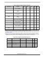
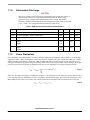
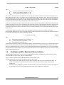
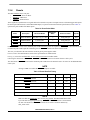
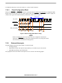
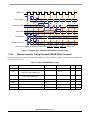
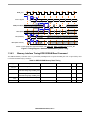
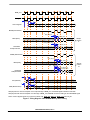
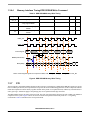
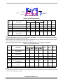
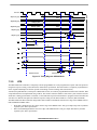
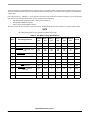
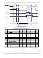
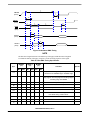
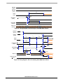
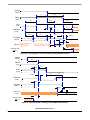
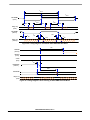
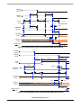
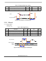
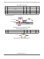
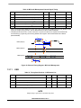
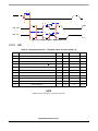
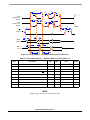
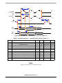
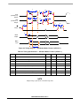
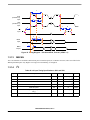
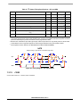
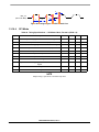
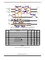
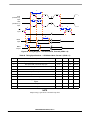
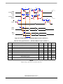
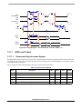
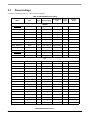
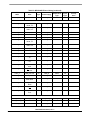
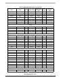
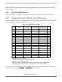
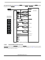
1
10
SCK
(CLKPOL=0)
Output
2
2
11
SCK
(CLKPOL=1)
Output
11
10
9
8
3
SS
Output
5
4
MOSI
Output
6
6
MISO
Input
7
7
Figure 32. Timing Diagram — SPI Master Mode, Format 0 (CPHA = 0)
Table 37. Timing Specifications — SPI Slave Mode, Format 0 (CPHA = 0)
Sym
Description
Min
Max
Units
1
Cycle time
4
1024
IP-Bus Cycle(1)
A11.12
(1)
A11.13
2
Clock high or low time
2
512
3
Slave select to clock delay
15.0
—
ns
A11.14
4
Output Data valid after Slave Select (SS)
—
50.0
ns
A11.15
5
Output Data valid after SCK
—
50.0
ns
A11.16
6
Input Data setup time
50.0
—
ns
A11.17
7
Input Data hold time
0.0
—
ns
A11.18
8
Slave disable lag time
15.0
—
ns
9
1
SpecID
Sequential Transfer delay
1
—
IP-Bus Cycle
A11.19
(1)
IP-Bus Cycle
A11.20
Inter Peripheral Clock is defined in the MPC5200B User’s Manual (MPC5200BUM).
NOTE
Output timing is specified at a nominal 50 pF load.
MPC5200B Data Sheet, Rev. 4
42
Freescale Semiconductor