1
4-2
UG-01169
2015.11.06
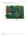
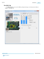
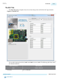
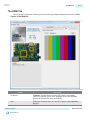
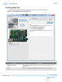
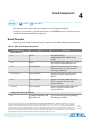
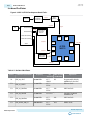
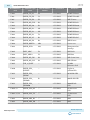
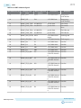
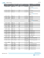
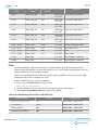
Board Overview
Board Reference
Type
Description
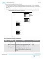
J14
10-pin header
Optional JTAG direct via 10-pin header for
external download cables.
J20
2x10-pin header
16 dual-purpose ADC channels are
connected to the 2x10 header.
SW2
DIP configuration and user
switch
SW2 Includes switches to control boot
images, JTAG bypass and HSMC bypass.
J7
Jumper for the MAX 10 ADC
Connects potentiometer for providing
adjustable voltage to the ADC.
S5
Pulse_nconfig push button
Emulates pulsing the nCONFIG pin low to
trigger reconfiguration even though the
physical pin is unaffected.
S6
CPU reset push button
Default reset for the FPGA logic.
D1
Blue power LED
Illuminates when 12-V power is present.
D2
Green high-speed mezzanine
card (HSMC) LED
Illuminates when the HSMC is present.
D13, D14
Green USB-UART LEDs
Illuminates when the USB-UART
transmitter and receiver are in use.
D20
Configuration done LED
Illuminates when the FPGA is configured.
D21, D22, D23
Power LEDs
Indicates that 3.3 V, 2.5 V, 1.2 V are
powered up successfully.
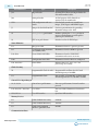
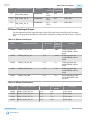
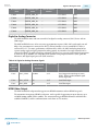
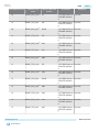
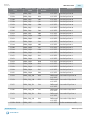
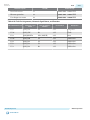
Status Elements
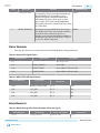
Clock Circuitry
X1
Programmable Clock for ADC Programmable oscillator for ADC with
default frequency of 10 MHz.
U2
Programmable Clock
Four channel programmable oscillator with
default frequencies of 25, 50, 100, 125 MHz.
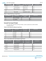
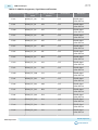
S1, S2, S3, S4
General user push buttons
Four user push buttons. Driven low when
pressed.
D15, D16, D17, D18, D19
User LEDs
Four user LEDs. Illuminates when driven
low.
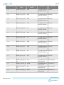
SW1, SW2.1
User DIP switches
Quad user DIP switches.
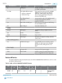
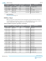
U5
DDR3 SDRAM A memory
64 Mx16.
U6
DDR3 SDRAM B memory
128 Mx8.
U7
Quad serial peripheral
interface (quad SPI) flash
512 Mb.
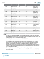
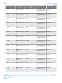
General User Input/Output
Memory Devices
Communication Ports
Altera Corporation
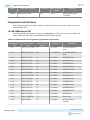
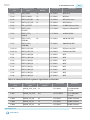
Board Components
Send Feedback