1
4-22
UG-01169
2015.11.06
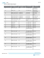
HSMC
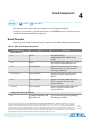
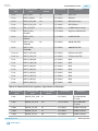
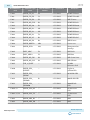
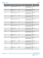
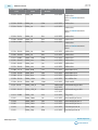
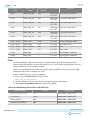
Board Reference (J2)
Schematic Signal
Name
MAX 10 / MAX II Pin
Number
I/O Standard
Description
121
HSMC_TX_D_N11
V15
2.5V CMOS inout or Data bus
LVDS TX channelsn
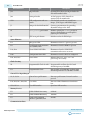
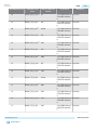
122
HSMC_RX_D_
N11(1)
AB16
2.5V CMOS inout or Data bus
LVDS RX channelsn
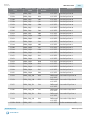
125
HSMC_TX_D_P12
V17
2.5v CMOS inout or
LVDS TX channelsp
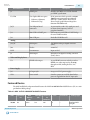
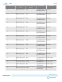
126
HSMC_RX_D_
P12(1)
AB18
2.5V CMOS inout or Data bus
LVDS RX channelsp
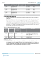
127
HSMC_TX_D_N12
W17
2.5V CMOS inout or Data bus
LVDS TX channelsn
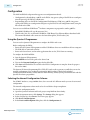
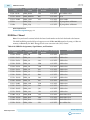
128
HSMC_RX_D_
N12(1)
AB17
2.5V CMOS inout or Data bus
LVDS RX channelsn
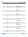
131
HSMC_TX_D_P13
V12
2.5v CMOS inout or
LVDS TX channelsp
132
HSMC_RX_D_
P13(1)
Y11
2.5V CMOS inout or Data bus
LVDS RX channelsp
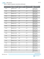
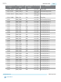
133
HSMC_TX_D_N13
V11
2.5V CMOS inout or Data bus
LVDS TX channelsn
134
HSMC_RX_D_
N13(1)
W11
2.5V CMOS inout or Data bus
LVDS RX channelsn
137
HSMC_TX_D_P14
P12
2.5v CMOS inout or
LVDS TX channelsp
138
HSMC_RX_D_
P14(1)
AB11
2.5V CMOS inout or Data bus
LVDS RX channelsp
139
HSMC_TX_D_N14
R12
2.5V CMOS inout or Data bus
LVDS TX channelsn
140
HSMC_RX_D_
N14(1)
AB10
2.5V CMOS inout or Data bus
LVDS RX channelsn
Altera Corporation
Data bus
Data bus
Data bus
Board Components
Send Feedback